Note: Descriptions are shown in the official language in which they were submitted.
CA 03147727 2022-01-14
WO 2021/026458
PCT/US2020/045417
1
TRANSPORTATION AND DETECTION OF ANALYTES
CROSS-REFERENCES TO RELATED APPLICATIONS
[0001] This application claims the benefit of United States Provisional Patent
Application Number 62/883,887 entitled "DEVICES AND METHODS FOR LABEL-
FREE DETECTION OF ANALYTES" and filed on August 7, 2019 for Regis Peytavi
et al.; and claims the benefit of United States Provisional Patent Application
Number
63/036,772 entitled "DYNAMIC EXCITATION AND MEASUREMENT OF
BIOCHEMICAL INTERACTIONS" and filed on June 9, 2020 for Kiana Aran et al.;
each of which is incorporated herein by reference in their entireties to the
extent legally
allowable.
FIELD
[0002] The subject matter disclosed herein relates to biotechnology and more
particularly relates to transportation and detection of analytes.
BACKGROUND
[0003] Various biochemical assays exist for detecting analytes, such as
certain
molecules or moieties. Certain assays may detect analytes in a liquid solution
when the
analytes are near a sensing surface. However, many analytes in the liquid
solution may
not be sufficiently close to the sensing surface to be detected.
SUMMARY
[0004] Systems are disclosed for transportation and detection of analytes. In
some embodiments, a chip-based field effect biosensor includes a sensing
surface. In
some embodiments, a sensing surface is configured so that one or more output
signals
for the chip-based field effect biosensor are affected by electrical charges
within a
measurement distance of the sensing surface, in response to application of one
or more
excitation conditions to the chip-based field effect biosensor and application
of a fluid
in contact with the sensing surface. In some embodiments, a bead control
device
includes one or more bead control components for electromagnetically
positioning a
plurality of beads within the fluid. In some embodiments, the beads may be
functionalized with a capture moiety to bind to a target moiety. In some
embodiments,
a measurement controller is configured to operate the chip-based field effect
biosensor
and the bead control device to perform a calibration measurement of at least
one of the
output signals with a first set of the beads positioned within the measurement
distance
of the sensing surface, where the first set of the beads has not been
incubated in a sample
CA 03147727 2022-01-14
WO 2021/026458
PCT/US2020/045417
2
solution. In some embodiments, the measurement controller is configured to
operate
the bead control device to remove the first set of the beads from the sensing
surface. In
some embodiments, the measurement controller is configured to operate the chip-
based
field effect biosensor and the bead control device to perform a detection
measurement
of the at least one output signal with a second set of the beads positioned
within the
measurement distance of the sensing surface, where the second set of the beads
has
been incubated in the sample solution. In some embodiments, an analysis module
is
configured to determine a parameter relating to presence of the target moiety
in the
sample solution, based on the calibration measurement and the detection
measurement.
[0005] Methods are disclosed for transportation and detection of analytes. In
some embodiments, a method includes providing a plurality of beads
functionalized
with a capture moiety to bind to a target moiety. In some embodiments, a
method
includes positioning a first set of the beads within a fluid to be within a
measurement
distance of a sensing surface of a chip-based field effect biosensor, where
the first set
of the beads has not been incubated in a sample solution. In some embodiments,
a
method includes performing a calibration measurement of at least one output
signal
from the chip-based field effect biosensor. In some embodiments, a method
includes
removing the first set of the beads from the sensing surface. In some
embodiments, a
method includes incubating a second set of the beads in the sample solution.
In some
embodiments, a method includes positioning the second set of the beads within
the fluid
to be within the measurement distance of the sensing surface. In some
embodiments, a
method includes performing a detection measurement of the at least one output
signal.
In some embodiments, a method includes determining a parameter relating to
presence
of the target moiety in the sample solution, based on the calibration
measurement and
the detection measurement.
[0006] Apparatuses are disclosed for transportation and detection of analytes.
In some embodiments, an apparatus includes means for positioning a plurality
of beads,
within a fluid, within a measurement distance of a sensing surface of a chip-
based field
effect biosensor, where the beads are functionalized with a capture moiety to
bind to a
target moiety. In some embodiments, an apparatus includes means for performing
a
calibration measurement using the chip-based field effect biosensor, with a
first set of
the beads positioned within the measurement distance of the sensing surface,
where the
first set of the beads has not been incubated in a sample solution. In some
embodiments,
an apparatus includes means for performing a detection measurement using the
chip-
based field effect biosensor, with a second set of the beads positioned within
the
CA 03147727 2022-01-14
WO 2021/026458
PCT/US2020/045417
3
measurement distance of the sensing surface, where the second set of the beads
has
been incubated in the sample solution.
BRIEF DESCRIPTION OF THE DRAWINGS
[0007] In order that the advantages of the invention will be readily
understood,
a more particular description of the invention briefly described above will be
rendered
by reference to specific embodiments that are illustrated in the appended
drawings.
Understanding that these drawings depict only typical embodiments of the
invention
and are not therefore to be considered to be limiting of its scope, the
invention will be
described and explained with additional specificity and detail through the use
of the
accompanying drawings, in which:
[0008] Figure 1 is a schematic block diagram illustrating one embodiment of a
system for transportation and detection of analytes;
[0009] Figure 2 is a schematic block diagram illustrating one embodiment of an
apparatus for transportation and detection of analytes, including one
embodiment of a
biologically gated transistor;
[0010] Figure 3 is a schematic block diagram illustrating another embodiment
of an apparatus for transportation and detection of analytes, including
another
embodiment of a biologically gated transistor;
[0011] Figure 4 is a schematic block diagram illustrating a further embodiment
.. of an apparatus for transportation and detection of analytes, including
embodiments of
beads and bead control components;
[0012] Figure 5 is a schematic block diagram illustrating another embodiment
of an apparatus for transportation and detection of analytes, including
embodiments of
beads and bead control components;
[0013] Figure 6 is a side view illustrating one embodiment of beads;
[0014] Figure 7 is a detail view of a region indicated in Figure 4,
illustrating
beads and a sensing surface during a calibration measurement, in one
embodiment;
[0015] Figure 8 is a detail view of a region indicated in Figure 4,
illustrating
removal of beads from a sensing surface, in one embodiment;
[0016] Figure 9 is a detail view of a region indicated in Figure 4,
illustrating
beads and a sensing surface during incubation, in one embodiment;
[0017] Figure 10 is a detail view of a region indicated in Figure 4,
illustrating
beads and a sensing surface during a detection measurement, in one embodiment;
[0018] Figure 11 is a schematic block diagram illustrating one embodiment of
an apparatus including a bead control device and a measurement controller;
CA 03147727 2022-01-14
WO 2021/026458
PCT/US2020/045417
4
[0019] Figure 12 is a schematic flow chart diagram illustrating one embodiment
of a method for transportation and detection of analytes;
[0020] Figure 13 is a schematic flow chart diagram illustrating another
embodiment of a method for transportation and detection of analytes; and
[0021] Figure 14 is a schematic flow chart diagram illustrating another
embodiment of a method for transportation and detection of analytes.
DETAILED DESCRIPTION
[0022] As will be appreciated by one skilled in the art, aspects of the
disclosure
may be embodied as a system, method, or program product. Accordingly,
embodiments
may take the form of an entirely hardware embodiment, an entirely software
embodiment (including firmware, resident software, micro-code, etc.) or an
embodiment combining software and hardware aspects that may all generally be
referred to herein as a "circuit," "module," or "system." Furthermore,
embodiments
may take the form of a program product embodied in one or more computer
readable
storage devices storing machine readable code, computer readable code, and/or
program code, referred hereafter as code. The storage devices may be tangible,
non-
transitory, and/or non-transmission. The storage devices may not embody
signals. In a
certain embodiment, the storage devices only employ signals for accessing
code.
[0023] Certain of the functional units described in this specification have
been
labeled as modules, in order to more particularly emphasize their
implementation
independence. For example, a module may be implemented as a hardware circuit
comprising custom VLSI circuits or gate arrays, off-the-shelf semiconductors
such as
logic chips, transistors, or other discrete components. A module may also be
implemented in programmable hardware devices such as field programmable gate
arrays, programmable array logic, programmable logic devices or the like.
[0024] Modules may also be implemented in code and/or software for execution
by various types of processors. An identified module of code may, for
instance,
comprise one or more physical or logical blocks of executable code which may,
for
instance, be organized as an object, procedure, or function. Nevertheless, the
executables of an identified module need not be physically located together,
but may
comprise disparate instructions stored in different locations which, when
joined
logically together, comprise the module and achieve the stated purpose for the
module.
[0025] Indeed, a module of code may be a single instruction, or many
instructions, and may even be distributed over several different code
segments, among
CA 03147727 2022-01-14
WO 2021/026458
PCT/US2020/045417
different programs, and across several memory devices. Similarly, operational
data may
be identified and illustrated herein within modules, and may be embodied in
any
suitable form and organized within any suitable type of data structure. The
operational
data may be collected as a single data set, or may be distributed over
different locations
5 including
over different computer readable storage devices. Where a module or portions
of a module are implemented in software, the software portions are stored on
one or
more computer readable storage devices.
[0026] Any combination of one or more computer readable medium may be
utilized. The computer readable medium may be a computer readable storage
medium.
The computer readable storage medium may be a storage device storing the code.
The
storage device may be, for example, but not limited to, an electronic,
magnetic, optical,
electromagnetic, infrared, holographic, micromechanical, or semiconductor
system,
apparatus, or device, or any suitable combination of the foregoing.
[0027] More specific examples (a non-exhaustive list) of the storage device
would include the following: an electrical connection having one or more
wires, a
portable computer diskette, a hard disk, a random access memory (RAM), a read-
only
memory (ROM), an erasable programmable read-only memory (EPROM or Flash
memory), a portable compact disc read-only memory (CD-ROM), an optical storage
device, a magnetic storage device, or any suitable combination of the
foregoing. In the
context of this document, a computer readable storage medium may be any
tangible
medium that can contain, or store a program for use by or in connection with
an
instruction execution system, apparatus, or device.
[0028] Code for carrying out operations for embodiments may be written in any
combination of one or more programming languages including an object oriented
programming language such as Python, Ruby, Java, Smalltalk, C++, or the like,
and
conventional procedural programming languages, such as the "C" programming
language, or the like, and/or machine languages such as assembly languages.
The code
may execute entirely on the user's computer, partly on the user's computer, as
a stand-
alone software package, partly on the user's computer and partly on a remote
computer
or entirely on the remote computer or server. In the latter scenario, the
remote computer
may be connected to the user's computer through any type of network, including
a local
area network (LAN) or a wide area network (WAN), or the connection may be made
to
an external computer (for example, through the Internet using an Internet
Service
Provider).
CA 03147727 2022-01-14
WO 2021/026458
PCT/US2020/045417
6
[0029] A component, as used herein, comprises a tangible, physical, non-
transitory device. For example, a component may be implemented as a hardware
logic
circuit comprising custom VLSI circuits, gate arrays, or other integrated
circuits; off-
the-shelf semiconductors such as logic chips, transistors, or other discrete
devices;
and/or other mechanical or electrical devices. A component may also be
implemented
in programmable hardware devices such as field programmable gate arrays,
programmable array logic, programmable logic devices, or the like. A component
may
comprise one or more silicon integrated circuit devices (e.g., chips, die, die
planes,
packages) or other discrete electrical devices, in electrical communication
with one or
more other components through electrical lines of a printed circuit board
(PCB) or the
like. Each of the modules described herein, in certain embodiments, may
alternatively
be embodied by or implemented as a component.
[0030] A circuit, or circuitry, as used herein, comprises a set of one or more
electrical and/or electronic components providing one or more pathways for
electrical
current. In certain embodiments, circuitry may include a return pathway for
electrical
current, so that a circuit is a closed loop. In another embodiment, however, a
set of
components that does not include a return pathway for electrical current may
be referred
to as a circuit or as circuitry (e.g., an open loop). For example, an
integrated circuit may
be referred to as a circuit or as circuitry regardless of whether the
integrated circuit is
coupled to ground (as a return pathway for electrical current) or not. In
various
embodiments, circuitry may include an integrated circuit, a portion of an
integrated
circuit, a set of integrated circuits, a set of non-integrated electrical
and/or electrical
components with or without integrated circuit devices, or the like. In one
embodiment,
a circuit may include custom VLSI circuits, gate arrays, logic circuits, or
other
integrated circuits; off-the-shelf semiconductors such as logic chips,
transistors, or
other discrete devices; and/or other mechanical or electrical devices. A
circuit may also
be implemented as a synthesized circuit in a programmable hardware device such
as
field programmable gate array, programmable array logic, programmable logic
device,
or the like (e.g., as firmware, a netlist, or the like). A circuit may
comprise one or more
silicon integrated circuit devices (e.g., chips, die, die planes, packages) or
other discrete
electrical devices, in electrical communication with one or more other
components
through electrical lines of a printed circuit board (PCB) or the like. Each of
the modules
described herein, in certain embodiments, may be embodied by or implemented as
a
circuit.
CA 03147727 2022-01-14
WO 2021/026458
PCT/US2020/045417
7
[0031] Reference throughout this specification to "one embodiment," "an
embodiment," or similar language means that a particular feature, structure,
or
characteristic described in connection with the embodiment is included in at
least one
embodiment. Thus, appearances of the phrases "in one embodiment," "in an
embodiment," and similar language throughout this specification may, but do
not
necessarily, all refer to the same embodiment, but mean "one or more but not
all
embodiments" unless expressly specified otherwise. The terms "including,"
"comprising," "having," and variations thereof mean "including but not limited
to,"
unless expressly specified otherwise. An enumerated listing of items does not
imply
that any or all of the items are mutually exclusive, unless expressly
specified otherwise.
The terms "a," "an," and "the" also refer to "one or more" unless expressly
specified
otherwise.
[0032] Furthermore, the described features, structures, or characteristics of
the
embodiments may be combined in any suitable manner. In the following
description,
numerous specific details are provided, such as examples of programming,
software
modules, user selections, network transactions, database queries, database
structures,
hardware modules, hardware circuits, hardware chips, etc., to provide a
thorough
understanding of embodiments. One skilled in the relevant art will recognize,
however,
that embodiments may be practiced without one or more of the specific details,
or with
other methods, components, materials, and so forth. In other instances, well-
known
structures, materials, or operations are not shown or described in detail to
avoid
obscuring aspects of an embodiment.
[0033] Aspects of the embodiments are described below with reference to
schematic flowchart diagrams and/or schematic block diagrams of methods,
apparatuses, systems, and program products according to embodiments. It will
be
understood that each block of the schematic flowchart diagrams and/or
schematic block
diagrams, and combinations of blocks in the schematic flowchart diagrams
and/or
schematic block diagrams, can be implemented by code. This code may be
provided to
a processor of a general purpose computer, special purpose computer, or other
programmable data processing apparatus to produce a machine, such that the
instructions, which execute via the processor of the computer or other
programmable
data processing apparatus, create means for implementing the functions/acts
specified
in the schematic flowchart diagrams and/or schematic block diagrams block or
blocks.
[0034] The code may also be stored in a storage device that can direct a
computer, other programmable data processing apparatus, or other devices to
function
CA 03147727 2022-01-14
WO 2021/026458
PCT/US2020/045417
8
in a particular manner, such that the instructions stored in the storage
device produce
an article of manufacture including instructions which implement the
function/act
specified in the schematic flowchart diagrams and/or schematic block diagrams
block
or blocks.
[0035] The code may also be loaded onto a computer, other programmable data
processing apparatus, or other devices to cause a series of operational steps
to be
performed on the computer, other programmable apparatus or other devices to
produce
a computer implemented process such that the code which execute on the
computer or
other programmable apparatus provide processes for implementing the
functions/acts
specified in the flowchart and/or block diagram block or blocks.
[0036] The schematic flowchart diagrams and/or schematic block diagrams in
the Figures illustrate the architecture, functionality, and operation of
possible
implementations of apparatuses, systems, methods, and program products
according to
various embodiments. In this regard, each block in the schematic flowchart
diagrams
and/or schematic block diagrams may represent a module, segment, or portion of
code,
which comprises one or more executable instructions of the code for
implementing the
specified logical function(s).
[0037] It should also be noted that, in some alternative implementations, the
functions noted in the block may occur out of the order noted in the Figures.
For
example, two blocks shown in succession may, in fact, be executed
substantially
concurrently, or the blocks may sometimes be executed in the reverse order,
depending
upon the functionality involved. Other steps and methods may be conceived that
are
equivalent in function, logic, or effect to one or more blocks, or portions
thereof, of the
illustrated Figures.
[0038] Although various arrow types and line types may be employed in the
flowchart and/or block diagrams, they are understood not to limit the scope of
the
corresponding embodiments. Indeed, some arrows or other connectors may be used
to
indicate only the logical flow of the depicted embodiment. For instance, an
arrow may
indicate a waiting or monitoring period of unspecified duration between
enumerated
steps of the depicted embodiment. It will also be noted that each block of the
block
diagrams and/or flowchart diagrams, and combinations of blocks in the block
diagrams
and/or flowchart diagrams, can be implemented by special purpose hardware-
based
systems that perform the specified functions or acts, or combinations of
special purpose
hardware and code.
CA 03147727 2022-01-14
WO 2021/026458
PCT/US2020/045417
9
[0039] The description of elements in each figure may refer to elements of
proceeding figures. Like numbers refer to like elements in all figures,
including
alternate embodiments of like elements.
[0040] As used herein, a list with a conjunction of "and/or" includes any
single
item in the list or a combination of items in the list. For example, a list of
A, B and/or
C includes only A, only B, only C, a combination of A and B, a combination of
B and
C, a combination of A and C or a combination of A, B and C. As used herein, a
list
using the terminology "one or more of' includes any single item in the list or
a
combination of items in the list. For example, one or more of A, B and C
includes only
A, only B, only C, a combination of A and B, a combination of B and C, a
combination
of A and C or a combination of A, B and C. As used herein, a list using the
terminology
"one of' includes one and only one of any single item in the list. For
example, "one of
A, B and C" includes only A, only B or only C and excludes combinations of A,
B and
C. As used herein, "a member selected from the group consisting of A, B, and
C,"
includes one and only one of A, B, or C, and excludes combinations of A, B,
and C."
As used herein, "a member selected from the group consisting of A, B, and C
and
combinations thereof' includes only A, only B, only C, a combination of A and
B, a
combination of B and C, a combination of A and C or a combination of A, B and
C.
[0041] Definitions:
[0042] The term "chip-based field effect biosensor," as used herein, refers to
a
sensor that includes a sensing surface on a substrate, such that when a fluid
is applied
in contact with the sensing surface, an output signal for the biosensor is
capable of being
modulated or affected by electric and/or magnetic fields in a fluid, proximate
to the
sensing surface. For example, ions or polar molecules within the fluid may
affect the
electric field near the sensing surface, thus affecting an output signal such
as a voltage,
current, impedance, capacitance, or the like. The term "biosensor" may refer
to such a
device in use, with a fluid applied to the sensing surface, or to the same
device before
the fluid has been applied. The term "biosensor" may be used without regard to
whether
molecules or moieties within the fluid are biologically produced. For example,
a
biosensor may be used to sense biologically produced or synthetically produced
molecules or moieties in the fluid, but may in either case still be referred
to as a
"biosensor."
[0043] The term "biologically gated transistor," as used herein, refers to a
type
of chip-based field effect biosensor, configured as a transistor where current
between
source and drain terminals, through at least one channel, is capable of being
gated,
CA 03147727 2022-01-14
WO 2021/026458
PCT/US2020/045417
modulated, or affected by events, occurrences, or interactions within a fluid
in contact
with a surface of the channel. Thus, a channel surface is a sensing surface
for the
biosensor. For example, an interaction of ions, molecules, or moieties within
the fluid,
or an interaction between the channel surface and ions, molecules, or moieties
within
5 the fluid,
may be capable of gating, modulating, or effecting the channel current. The
term "biologically gated transistor" may be used to refer to such a device in
use, with a
fluid applied to the surface of the channel, or to the same device before the
fluid has
been applied. The term "biologically gated transistor" may be used without
regard to
whether molecules or moieties within the fluid are biologically produced. For
example,
10 a
biologically gated transistor may be gated by interactions between a
biologically
produced enzyme in the fluid and the enzyme's substrate, or may be gated by
non-
biological interactions within the fluid, but may still be referred to as
"biologically
gated."
[0044] The term "output signal," as used herein, refers to a measurable or
detectable electrical signal from a chip-based field effect biosensor, or to a
result that
can be calculated based on the measurable or detectable signal. For example,
an output
signal may be a voltage at one or more terminals of a chip-based field effect
biosensor,
a current at one or more chip-based field effect biosensor, a capacitance,
inductance, or
resistance (calculated based on applied and measured voltages and currents), a
complex-valued impedance, a complex impedance spectrum, an electrochemical
impedance spectrum, a threshold voltage, a Dirac voltage, a power spectral
density, one
or more network parameters (such as S-parameters or h-parameters), or the
like.
[0045] The term "distance," as used herein with reference to a distance from a
surface such as a sensing surface in a chip-based field effect biosensor or
the surface of
a channel in a biologically gated transistor, refers to a distance between a
point (e.g., in
the fluid applied to a biosensor), and the closest point of the surface to
that point. For
example, the distance from a sensing surface to a point directly above the
sensing
surface in the applied fluid is the distance between a point on the sensing
surface to the
point in the fluid, along a line that is normal (perpendicular) to the sensing
surface.
[0046] The term "measurement distance," as used herein, refers to a distance
from the sensing surface in a chip-based field effect biosensor, such that at
least some
interaction, molecule or moiety occurring at or within the measurement
distance affects
an output signal in a way that is detectable by a measurement controller. In
other words,
output signals from a chip-based field effect biosensor are sensitive to
charges (e.g., of
ions or within moieties, molecules, or complexes of molecules) within the
measurement
CA 03147727 2022-01-14
WO 2021/026458
PCT/US2020/045417
11
distance. Whether an effect on an output signal is detectable by a measurement
controller may depend on actual sensitivity of the measurement controller, on
a noise
level for noise in the output signal, the extent to which the output signal is
affected by
events or occurrences closer to the sensing surface, or the like. Whether an
effect on an
output signal is detectable by a measurement controller may be based on a
predetermined threshold for detection or sensitivity, which may be signal to
noise ratio,
a ratio between effects on the output signal caused by events at a distance
from the
surface to effects on the output signal caused by events at the sensing
surface, or the
like. In some examples, a measurement distance may depend on excitation
conditions,
or may be frequency dependent.
[0047] The term "within the measurement distance," as used herein, refers to
objects within a fluid applied to chip-based field effect biosensor, such that
a distance
from the sensing surface to at least a portion of such an object is less than
the
measurement distance. For example, a bead in the fluid may be referred to as
being
within the measurement distance, if at least a part of the bead is closer than
the
measurement distance to the surface. Such a bead may be entirely within the
measurement distance, or may include a portion that extends further away from
the
sensing surface than the measurement distance.
[0048] The term "excitation condition," as used herein, refers to a physical,
electrical, or chemical condition applied to a chip-based field effect
biosensor or to a
sample for measurement by a chip-based field effect biosensor. Excitation
conditions
may affect a state of a molecules or moieties in the fluid applied to the
biosensor, which
in turn may affect one or more output signals from the biosensor. For example,
excitation conditions may include voltages, currents, frequencies, amplitudes,
phases,
or waveforms of electrical signals applied to a biologically gated transistor,
one or more
temperatures, one or more fluid flow rates, one or more wavelengths of
electromagnetic
radiation, or the like.
[0049] The term "beads," as used herein, refers to particles in the range of
about
mm to 10p,m in diameter having a functionalized surface configured to bind
with a
corresponding component of a molecule or moiety in solution. Some beads are
magnetic and other beads are non-magnetic. Non-limiting examples of beads
include
particles functionalized with a streptavidin coating configured to bind with
biotinylated
molecules in solution. Other non-limiting examples of materials for
functionalizing a
bead surface include antibodies, biotin, proteins that bind to biotin, zinc
finger proteins,
CA 03147727 2022-01-14
WO 2021/026458
PCT/US2020/045417
12
CRISPR Cas family enzymes, nucleic acids, and synthetic nucleic acid analogs
such as
peptide nucleic acid, xeno nucleic acid, and the like.
[0050] The term "moiety," as used herein, refers to a part of a molecule. For
example, a moiety may be a biotin portion of a biotinylated molecule, a
streptavidin
moiety linked to a surface of a bead, or the like. In the plural form, the
term "moieties"
may be used to refer to multiple types of moiety (e.g., a capture moiety and a
target
moiety) or to multiple instances of the same type of moiety for multiple
molecules (e.g.,
multiple instances of the a target moiety).
[0051] The term "target moiety," as used herein refers to a moiety of an
analyte,
which may be a molecule or molecular complex for which the presence, absence,
concentration, activity, or other parameters relating to the analyte may be
determined
in an assay or test. For example, an assay using a chip-based field effect
biosensor may
be used to determine the presence, absence, or concentration of an analyte
that includes
the target moiety.
[0052] The term "capture moiety," as used herein, refers to a moiety with an
affinity for binding to a target moiety. For example, the capture moiety may
be a biotin-
binding protein when the target moiety is biotin, or may be an RNA-guided Cos
enzyme
when the target moiety is a nucleic acid sequence. Conversely, the capture
moiety may
be biotin when the target moiety is a biotin-binding protein, or may be a
nucleic acid
sequence when the target moiety is an RNA-guided Cas enzyme.
[0053] Various biochemical assays exist for detecting analytes, such as
certain
molecules or moieties. Certain assays may detect analytes in a liquid solution
when the
analytes are near a sensing surface. However, when analytes are large
molecules,
diffusion of the analytes in the liquid solution may not bring enough of the
analytes
close enough to the sensing surface to be detected.
[0054] Additionally, some assays may involve functionalization of the sensing
surface to capture or bind to the analytes. However, a sensing surface, once
functionalized to bind to a particular analyte, may be unsuited for
measurement of other
analytes, with the result that manufacturers may make expensive single-purpose
sensors
rather than low-cost sensors capable of being used for multiple assays. Also
where a
functionalized sensing surface or an analyte is labeled with a fluorescent or
colorimetric
label to optically detect the binding of the analyte to the sensing surface,
reagents for
labeling, time for labeling reactions, and optical components for detection
may add
significantly to the time, complexity and expense of an assay.
CA 03147727 2022-01-14
WO 2021/026458
PCT/US2020/045417
13
[0055] By contrast, assays using chip-based field effect biosensors, as
disclosed
herein, with beads to capture target moieties and bead control components to
position
the beads near the sensing surface, may efficiently and inexpensively
transport and
detect analytes. Chip-based field effect biosensors may be built using
traditional
electronics manufacturing techniques, leading to lower costs. Systems using
chip-
based field effect biosensors may be capable of performing electronic target
detection
for a wide variety of targets, leading to lower overall cost for individual
assays.
[0056] Figure 1 is a schematic block diagram illustrating one embodiment of a
system 100 for transportation and detection of analytes. The system 100, in
the depicted
embodiment, includes one or more chip-based field effect biosensors 104, a
chip reader
device 102, a sample prep apparatus 112, a computing device 114, a remote data
repository 118, and a data network 120.
[0057] In the depicted embodiment, a chip-based field effect biosensor 104, in
the depicted embodiment, includes one or more biologically gated transistors
106,
which are described in further detail below. In various embodiments, a chip-
based field
effect biosensor 104 may include one or more sensing surfaces, arranged on a
solid
support. In a biologically gated transistor 106, a sensing surface may be a
surface of a
channel that couples a drain terminal to a source terminal. In a capacitive or
electrochemical sensor, a sensing surface may be a surface of a working
electrode, and
the chip-based field effect biosensor 104 may include an electrochemical
system with
a reference electrode to measure an electrochemical potential and a counter
electrode
to modify an electrochemical potential.
[0058] One or more layers of ions may form near the sensing surface when a
fluid is applied in contact with the sensing surface. For example, a double
layer of ions
may include a first layer of ions attracted or adsorbed to the sensing surface
and a
second layer of ions attracted to the ions in the first layer. Or, if the
surface has been
functionalized by immobilizing certain molecules or moieties (e.g., proteins,
peptides,
surfactants, polymers such as polyethylene glycol, or the like) to the sensing
surface,
forming an ion-permeable layer with a net charge, then ions from the fluid may
diffuse
into the ion-permeable layer of immobilized molecules or moieties due to the
Gibbs-
Donnan effect, forming a Donnan equilibrium region. In either case, charges
near the
sensing surface may act as a dielectric between the channel of a biologically
gated
transistor 106, or the working electrode of a capacitive sensor, and the bulk
of the
applied fluid.
CA 03147727 2022-01-14
WO 2021/026458
PCT/US2020/045417
14
[0059] When excitation conditions are applied to a chip-based field effect
biosensor 104, output signals such as a channel current or capacitance may
depend on
charges within this (effective) dielectric layer, or more generally within a
measurement
distance of the sensing surface. Charges within a measurement distance of the
sensing
surface, which affect the output signals of the biosensor 104, may be
positively or
negatively charged ions or moieties, or may be neutrally charged molecules or
moieties
(e.g., including an equal number of positive and negative charges) that
displace other
charges. For example, if the fluid applied to the chip-based field effect
biosensor 104
includes DNA molecules with negatively charged phosphate groups, then
transporting
the DNA molecules to be near or in contact with the sensing surface brings
negative
charges within the measurement distance, thus affecting the output signal(s)
for the
biosensor 104.
[0060] In some embodiments, a chip-based field effect biosensor 104 may
include a plurality of transistors where at least one of the transistors is a
biologically
gated transistor 106. In some embodiments, a chip-based field effect biosensor
104 may
include one or more additional sensors that do not use field-effect sensing,
alongside
sensors with sensing surfaces for field-effect sensing. For example, various
types of
sensors may be included that use terahertz spectroscopy, surface-enhanced
spectroscopy, quartz crystal microbalance, grating-coupled interferometry, and
so
forth. In some embodiments, a chip-based field effect biosensor 104 may
include
further components such as a flow cell or fluid propulsion mechanism.
[0061] In the depicted embodiment, the chip reader device 102 includes
circuitry for communicating with (e.g., sending electrical signals to or
receiving
electrical signals from) components of the chip-based field effect biosensor
104. For
example, a chip-based field effect biosensor 104 may include a chip or
integrated circuit
with one or more biologically gated transistors 106, mounted to a printed
circuit board
with electrical contacts at one edge. A socket in the chip reader device 102
may include
matching contacts, so that the chip-based field effect biosensor 104 can be
plugged into
or removed from the chip reader device 102. Various other or further types of
connectors may be used to provide a detachable coupling between a chip-based
field
effect biosensor 104 and a chip reader device 102.
[0062] In a further embodiment, the chip reader device 102 may include
circuitry for communicating via the data network 120. For example, the chip
reader
device 102 may communicate information about measurements performed using the
chip-based field effect biosensor 104 to the computing device 114 and/or to a
remote
CA 03147727 2022-01-14
WO 2021/026458
PCT/US2020/045417
data repository 118, over the data network. The data network 120, in various
embodiments, may be the Internet, or may be another network such as a wide
area
network, metropolitan area network, local area network, virtual private
network, or the
like. In another embodiment, the chip reader device 102 may communicate
information
5 in another
way, in addition to or in place of communicating over a data network 120.
For example, the chip reader device 102 may display or print information, save
information to a removable data storage device, or the like.
[0063] In the depicted embodiment, a bead control device 122 and a
measurement controller 124 are implemented by the chip-based field effect
biosensor
10 104 and/or the chip reader device 102.
[0064] A bead control device 122, in various embodiments, may include one or
more bead control components for electromagnetically positioning a plurality
of beads,
within a fluid applied to a chip-based field effect biosensor 104. Beads may
be
functionalized with a capture moiety to bind to a target moiety, as discussed
in further
15 detail with
reference to subsequent figures, and may be controlled to bring the beads
within the measurement distance of a sensing surface chip-based field effect
biosensor
104. Thus, in various embodiments, beads may bind to an analyte, and may be
electromagnetically positioned to bring the analyte close to the sensing
surface to be
detected.
[0065] -Electromagnetically positioning beads, in various embodiments, may
include using electric and/or magnetic fields to move beads, or to limit or
constrain the
motion of beads. For example, bead control components that electromagnetically
position beads may be electromagnets that can be controlled to move magnetic
beads
toward or away form a surface, or to hold magnetic beads onto a surface (e.g.,
during
fluid flow to wash the beads). As another example, bead control components
that
electromagnetically position beads may be a pair of parallel conductive plates
(or other
conductors) configured so that applying a different voltage to each of the
conductors
produces an electric field between the conductors, to move electrically
charged beads
or to limit the motion of the beads by attracting or repelling them. Various
other or
further components for producing electric and/or magnetic fields may be used
as bead
control components.
[0066] Additionally, in various embodiments, a bead control device 122 may
include circuitry for controlling bead control components. For example, a bead
control
device 122 may include power supply components, current sources or regulators
for
controlling electromagnets, voltage sources or regulators for applying an
electric
CA 03147727 2022-01-14
WO 2021/026458
PCT/US2020/045417
16
potential to field plates, control circuitry for applying, removing, or
modulating power
to the bead control components, or the like.
[0067] A measurement controller 124, in various embodiments, may include
excitation circuitry to apply excitation conditions to a chip-based field
effect biosensor
104, including a biologically gated transistor 106 or a capacitive sensor.
Output signals
from the chip-based field effect biosensor 104 (such as electrical currents,
voltages,
capacitances, impedances, or the like) may be affected by charges within the
measurement distance of a sensing surface, in response to the excitation
conditions and
the application of a fluid in contact with the sensing surface. For example,
if the applied
fluid contains biotinylated DNA, and if beads with a capture moiety that binds
to the
target biotin moiety are incubated in the fluid and brought within the
measurement
distance, then the negative charge of the DNA bound to the beads may affect
one or
more of the output signals. The measurement controller 124 may include
measurement
circuitry to perform one or more measurements of at least one of the output
signals that
are affected by the charges within the measurement distance. Various
embodiments of
a measurement controller 124 are described in further detail below.
[0068] In some embodiments, a chip-based field effect biosensor 104 may
include the bead control device 122 and/or the measurement controller 124. For
example, bead control components, excitation circuitry and/or measurement
circuitry
may be provided on the same chip as a biologically gated transistor 106 or a
capacitive
sensor, or on the same package, on the same printed circuit board, or the
like, as part of
a chip-based field effect biosensor 104. In another embodiment, the chip
reader device
102 may include the bead control device 122 and/or the measurement controller
124.
For example, bead control components, excitation circuitry and/or measurement
circuitry may be provided in a chip reader device 102 so as to be reusable
with multiple
chip-based field effect biosensors 104.
[0069] In another embodiment, a chip-based field effect biosensor 104 and a
chip reader device 102 may both include portions of the bead control device
122 and/or
the measurement controller 124. For example, the chip-based field effect
biosensor 104
may include portions of the bead control device 122 such as an electromagnet
proximate
to the sensing surface for positioning beads within the measurement distance
of the
sensing surface, and the and the chip reader device 102 may include other
portions of
the bead control device 122 such as an electromagnet for removing beads from
the
sensing surface. In various embodiments, portions of the bead control device
122
CA 03147727 2022-01-14
WO 2021/026458
PCT/US2020/045417
17
and/or the measurement controller 124 may be disposed between a chip-based
field
effect biosensor 104 and a chip reader device 102 in various other or further
ways.
[0070] Additionally, although the system 100 in the depicted embodiment
includes a chip-based field effect biosensor 104 that may be coupled to or
removed
from a chip reader device 102, the functions and/or components of a chip-based
field
effect biosensor 104 and a chip reader device 102 may be integrated into a
single device
in another embodiment. Conversely, in some embodiments, a system may include
multiple devices rather than a single chip reader device 102. For example,
excitation
circuitry and/or measurement circuitry for a measurement controller 124 may
include
lab bench hardware such as source measure units, function generators, bias
tees,
chemical impedance analyzers, lock-in amplifiers, data acquisition devices, or
the like,
which may be coupled to a chip-based field effect biosensor 104.
[0071] The sample prep apparatus 112, in the depicted embodiment, is
configured to automatically or semi-automatically prepare a sample solution
110. An
assay using a chip-based field effect biosensor 104 may be used to determine a
parameter relating to presence of an analyte in the sample solution, such as
the presence,
absence, or concentration of an analyte. Thus, preparation of the sample
solution 110
may include preparing a solution in which the analyte may or may not be
present. In
some embodiments, a sample prep apparatus 112 may include automated dispensing
equipment such as a dispensing robot and/or a fluidic system. In some
embodiments, a
sample prep apparatus 112 may include its own controller and user interface
for setting
sample prep parameters such as incubation time and temperature for the sample
solution
110. In some embodiments, a sample prep apparatus 112 may be controlled via
the data
network 120. For example, the computing device 114 or the measurement
controller
124 may control the sample prep apparatus 112.
[0072] In another embodiment, a system 100 may omit a sample prep apparatus
112, and a sample solution 110 may be manually prepared. In some embodiments,
preparing a sample solution 110 may include obtaining or preparing a sample of
a fluid
in which an analyte may be observed (or the absence of an analyte may be
detected). In
some embodiments, preparing a sample solution 110 may include incubation of
beads
in the sample solution. In some embodiments, a sample solution 110 may be a
biological sample such as blood, urine, saliva, or the like, directly obtained
without
further sample prep steps. In another embodiment, further sample prep steps to
prepare
a sample solution 110 may include the addition of reagents, concentration or
dilution,
heating or cooling, centrifuging, or the like. Various other or further
preparation
CA 03147727 2022-01-14
WO 2021/026458
PCT/US2020/045417
18
techniques may be used to prepare a sample solution 110 for use with a
measurement
controller 124.
[0073] The sample solution 110, in various embodiments, may include one or
more types of biomolecules 108. Biomolecules 108, in various embodiments, may
be
any molecules that are produced by a biological organism, including large
polymeric
molecules such as proteins, polysaccharides, lipids, and nucleic acids (DNA
and RNA)
as well as small molecules such as primary metabolites, secondary metabolites,
and
other natural products. Biomolecules 108 or other analytes may include target
moieties
capable of being bound to capture moieties of beads. For example, target
moieties may
include biotin or a DNA sequence, and may be bound to, respectively, by a
biotin-
binding protein (e.g., streptavidin, avidin, neutravidin, or the like), or by
an RNA
guided Cas enzyme. The presence or absence of analytes bound to the beads, or
related
parameter may be detected when the beads are positioned within the measurement
distance of a sensing surface.
[0074] The computing device 114, in the depicted embodiment, implements an
analysis module 116. In various embodiments, a computing device 114 may be a
laptop
computer, a desktop computer, a smartphone, a handheld computing device, a
tablet
computing device, a virtual computer, an embedded computing device integrated
into
an instrument, or the like. In further embodiment, a computing device 114 may
communicate with the measurement controller 124 via the data network 120. The
analysis module 116, in certain embodiments, is configured to determine a
parameter
relating to presence of the target moiety in the sample solution 110, based on
calibration
and detection measurements taken by the taken by the measurement controller
124 as
described below. In various embodiments, an analysis module 116 may determine
various parameters relating to the presence of a target moiety, such as a such
as an
indication of whether or not the target moiety (or an analyte including the
target moiety)
is present in the sample solution, a concentration of the target moiety (or an
analyte
including the target moiety), or another parameter corresponding to or related
to the
concentration, or the like.
[0075] In the depicted embodiment, the analysis module 116 is separate from
the measurement controller 124, and is implemented by a computing device 114
separate from the measurement controller 124. In another embodiment, the
analysis
module 116 may be partially or fully integrated with the measurement
controller 124.
For example, the measurement controller 124 may include special-purpose logic
hardware and/or a processor executing code stored in memory to implement all
or part
CA 03147727 2022-01-14
WO 2021/026458
PCT/US2020/045417
19
of the analysis module 116. In some embodiments, the analysis module 116 may
be
implemented as an embedded processor system or other integrated circuits that
form
part of a chip-based field effect biosensor 104 and/or part of a chip reader
device 102.
In some embodiments, where an analysis module 116 is integrated with the
measurement controller 124, a system 100 may omit a separate computing device
114.
[0076] The remote data repository 118, in various embodiments, may be a
device or set of devices remote from the measurement controller 124 and
capable of
storing data. For example, the remote data repository 118 may be, or may
include, a
hard disk drive, a solid-state drive, a drive array, or the like. In some
embodiments, the
remote data repository 118 may be a data storage device within the computing
device
114. In some embodiments, a remote data repository 118 may be network attached
storage, a storage area network, or the like.
[0077] In some embodiments, the measurement controller 124 (e.g., a chip-
based field effect biosensor 104 and/or a chip reader device 102) may include
communication circuitry that transmits measurement information to the remote
data
repository 118. Measurement information may be measurements from chip-based
field
effect biosensors 104, or information about the measurements, such as
calculated
quantities based on the raw measurements. The analysis module 116 may
communicate
with the remote data repository 118 to determine one or more parameters
relating to
presence of a target moiety based on the information stored by the remote data
repository 118. In further embodiments, the analysis module 116 may store
analysis
results to the remote data repository 118. In another embodiment, however, the
analysis
module 116 may receive measurement information from the measurement controller
124 directly or over the data network 120, and a remote data repository 118
may be
.. omitted (e.g., in favor of local data storage).
[0078] Figure 2 is a schematic block diagram illustrating one embodiment of an
apparatus 200 for transportation and detection of analytes by an enzyme,
including one
embodiment of a biologically gated transistor 106a, coupled to a bead control
device
122 and a measurement controller 124. The biologically gated transistor 106a
is
depicted in a top view. The biologically gated transistor 106a, the bead
control device
122, and the measurement controller 124 in the depicted embodiment may be
substantially as described above with reference to Figure 1, and are described
further
below.
[0079] The biologically gated transistor 106a, in the depicted embodiment,
includes a source 212, a drain 202, a channel 210, a reference electrode 208,
a counter
CA 03147727 2022-01-14
WO 2021/026458
PCT/US2020/045417
electrode 204, and a liquid well 206, which are described below. In general,
in various
embodiments, a biologically gated transistor 106a may include at least one
channel 210
capable of conducting an electrical current between the source 212 and the
drain 202.
As in an insulated-gate field-effect transistor, current between the source
212 and the
5 drain 202
depends not only not only on a voltage difference between the source 212
and the drain 202 but on certain conditions that affect the conductivity of
the channel
210. However, an insulated-gate field-effect transistor is a solid-state
device where a
gate electrode is separated from the channel by a thin dielectric layer, so
that the channel
conductivity is modulated by the gate-to-body (or gate-to-source) voltage.
Conversely,
10 in various
embodiments, channel conductivity (and a resulting drain-to-source current)
for a biologically gated transistor 106a may be modulated, gated, or affected
by liquid-
state events. In particular, a fluid may be applied to the biologically gated
transistor
106a in contact with the channel 210, so that the channel conductivity depends
on (or
is gated or modulated by) a state of moieties within the fluid.
15 [0080] In
various embodiments, the source 212, the drain 202, a channel 210, a
reference electrode 208, and a counter electrode 204 may be formed on a
substrate (not
shown), such as an oxide or other dielectric layer of a silicon wafer or chip.
Certain
components of the biologically gated transistor 106a may be formed to be in
contact
with a fluid. For example, upper surfaces of the channel 210, the reference
electrode
20 208 and the
counter electrode 204 may be exposed or bare for direct interaction with
the fluid. Other components may be covered or electrically insulated from the
fluid. For
example, the source 212 and drain 202 may be covered by an insulating layer
such as
silicon dioxide, silicon nitride, or another dielectric, so that current flows
between the
source 212 and drain 202 through the channel 210, without the fluid creating a
short
circuit or an alternative or unintended current path between the source 212
and drain
202.
[0081] The liquid well 206 may be a structure to contain the applied fluid in
a
region above the other components of the biologically gated transistor 106a.
For
example, the liquid well 206 may be a ridge of epoxy, a thermosetting resin, a
thermoplastic, or the like. The liquid well 206 may be deposited on the
substrate,
formed as an opening in the chip packaging for the biologically gated
transistor 106a,
or the like.
[0082] The channel 210, in some embodiments, includes a sensing surface
made of a highly sensitive conducting material such as graphene. In further
embodiments, a graphene channel 210 may be deposited on the substrate for the
CA 03147727 2022-01-14
WO 2021/026458
PCT/US2020/045417
21
biologically gated transistor 106a by chemical vapor deposition (CVD). In some
embodiments, the channel 210 may be made from another two-dimensional material
which has strong in-plane covalent bonding and weak interlayer interactions.
Such
materials may be referred to as van der Waals materials. For example, in
various
embodiments, a channel 210 may be made from graphene nanoribbons (GNR),
bilayer
graphene, phosphorene, stanine, graphene oxide, reduced graphene,
fluorographene,
molybdenum disulfide, gold, silicon, germanene, topological insulators, or the
like.
Various materials that conduct and exhibit field-effect properties, and are
stable at room
temperature when directly exposed to various solutions, may be used in a
biologically
gated transistor 106a. Materials that may be suitable for forming a channel
210 of a
biologically gated transistor 106a may include silicon surfaces, carbon
electrodes,
graphene, or two-dimensional materials other than graphene. Similar materials
may
also be used as sensing surfaces in electrochemical or capacitive sensors. In
various
implementations, using a biologically gated transistor 106a with one or more
channels
210 formed from planar two-dimensional van der Waals materials improves
manufacturability, and lowers costs compared with one-dimensional
alternatives, such
as carbon nanotubes.
[0083] The source 212 and drain 202 are disposed at opposite ends of the
channel 210 so that a current conducted through the channel 210 is conducted
from the
drain 202 to the source 212, or from the source 212 to the drain 202. In
various
embodiments, the source 212 and drain 202 may be made of conductive material
such
as gold, platinum, polysilicon, or the like. In some embodiments, the source
212 may
be coupled to the substrate of the biologically gated transistor 106a (e.g.,
the silicon
below the oxide or other dielectric layer) so that a bias voltage (or another
bias signal)
applied to the source 212 also biases the substrate under the channel 210. In
another
embodiment, a biologically gated transistor 106a may include a separate body
terminal
(not shown) for biasing the substrate.
[0084] The terms "source" and "drain" may be used herein to refer to
conductive regions or electrodes that directly contact the channel 210, or to
leads, wires
or other conductors connected to those regions or electrodes. Additionally,
the terms
"source" and "drain" are used as the conventional names for terminals of a
transistor,
but without necessarily implying a type of charge carrier. For example, a
graphene
channel 210 may conduct electricity with electrons or holes as the charge
carriers
depending on various external conditions (such as the excitation conditions
applied by
the measurement controller 124 and the charges within the measurement
distance), and
CA 03147727 2022-01-14
WO 2021/026458
PCT/US2020/045417
22
the charge carriers may flow from the source 212 to the drain 202, or from the
drain
202 to the source 212.
[0085] In various embodiments, one or more output signals from the
biologically gated transistor 106a may be affected by excitation conditions
and by
charges within a measurement distance of the channel surface. As defined
above, the
excitation conditions may be physical, electrical, or chemical conditions
applied to the
biologically gated transistor 106a. Excitation conditions such as constant
bias voltages
(or signals), time-varying excitation voltages (or signals), temperature
conditions, or
the like may be applied to the biologically gated transistor 106a or to the
applied fluid
by the measurement controller 124. When beads incubated in the sample solution
110
are positioned within the applied fluid to be within the measurement distance
of a
sensing surface (e.g., the channel surface), the charges within the
measurement distance
may depend on whether (or to what extent) an the target moiety was captured by
a
capture moiety functionalized to the beads, and thus may depend on the
presence,
absence, or concentration of the target moiety. The interaction of such
charges with the
channel 210 may gate or modulate the channel conductivity, affecting one or
more
output signals. The output signals may be, or may include, a channel current,
a voltage,
a capacitance, inductance, or resistance (calculated based on applied and
measured
voltages and currents), a complex-valued impedance, a complex impedance
spectrum,
an electrochemical impedance spectrum, a Dirac voltage, a power spectral
density, one
or more network parameters (such as S-parameters or h-parameters), or the
like.
[0086] In some embodiments, certain biomolecules or moieties may be
immobilized or functionalized to the surface of the channel 210 to react with
other
biomolecules or moieties that may be present in the applied fluid. However,
the use of
beads to capture and transport analytes to be within the measurement distance
may
allow the analyte to be detected with a bare or unfunctionalized channel 210,
or with a
channel 210 that is functionalized to react to a biomolecule or moiety other
than the
analyte or the target moiety.
[0087] In various embodiments, a fluid applied to the channel 210 may be
referred to as a liquid gate for the biologically gated transistor 106a,
because one or
more of the output signals for the biologically gated transistor 106a may be
affected by
charges within the liquid gate (e.g., charges within the measurement
distance). In
addition, in various embodiments, a biologically gated transistor 106a may
include one
or more gate electrodes for detecting and/or adjusting a voltage or electric
potential of
the liquid gate. For example, in the depicted embodiment, the biologically
gated
CA 03147727 2022-01-14
WO 2021/026458
PCT/US2020/045417
23
transistor 106a includes a reference electrode 208 for measuring an
electrochemical
potential of the applied fluid, and a counter electrode 204 for adjusting the
electrochemical potential of the applied fluid.
[0088] In some embodiments, an electric potential may develop at the interface
between the applied fluid and the reference electrode 208 and/or the counter
electrode
204. Thus, in some embodiments, a reference electrode 208 may be made of a
material
with a known or stable electrode potential. In another embodiment, however, a
reference electrode 208 may be a pseudo-reference electrode that does not
maintain a
constant electrode potential. Nevertheless, measurements of the
electrochemical
potential of the fluid via a pseudo-reference electrode may still be useful as
output
signals or as feedback for adjusting the electrochemical potential of the
fluid via the
counter electrode 204. In some embodiments, the reference electrode 208 and/or
the
counter electrode 204 may be made of non-reactive materials such as gold or
platinum.
[0089] In some embodiments, a biologically gated transistor 106a may be made
using photolithography or other commercially available chip fabrication
techniques.
For example, a thermal oxide layer may be grown on a silicon substrate, and
metal
components such as a source 212, drain 202, reference electrode 208 and/or the
counter
electrode 204 may be deposited or patterned on the thermal oxide layer. A
graphene
channel 210 may be formed using chemical vapor deposition. The use of
conventional
fabrication techniques may provide low-cost biologically gated transistors
106a,
especially in comparison to sensors using high-cost materials such as carbon
nanotubes
or specialty fabrication techniques. Various other or further configurations
of
biologically gated transistors 106a and ways to fabricate biologically gated
transistors
106a are discussed in United States Patent Application Number 15/623,279
entitled
"PATTERNING GRAPHENE WITH A HARD MASK COATING"; United States
Patent Application Number 15/623,295 entitled "PROVIDING A TEMPORARY
PROTECTIVE LAYER ON A GRAPHENE SHEET"; United States Patent
Application Number 16/522,566 entitled "SYSTEMS FOR TRANSFERRING
GRAPHENE"; and United States Patent Number 10,395,928 entitled "DEPOSITING
A PASSIVATION LAYER ON A GRAPHENE SHEET"; each of which is
incorporated herein by reference in their entireties to the extent legally
allowable.
[0090] Figure 3 is a schematic block diagram illustrating another embodiment
of an apparatus 300 for transportation and detection of analytes, including
another
embodiment of a biologically gated transistor 106b, coupled to a bead control
device
122 and a measurement controller 124. As in Figure 2, the biologically gated
transistor
CA 03147727 2022-01-14
WO 2021/026458
PCT/US2020/045417
24
106b is depicted in atop view. The biologically gated transistor 106b, the
bead control
device 122 and the measurement controller 124 in the depicted embodiment may
be
substantially as described above with reference to Figures 1 and 2, and are
described
further below.
[0091] In the depicted embodiment, the biologically gated transistor 106b
includes a source 312, a plurality of drains 302, a plurality of channels 210,
a reference
electrode 308, and a counter electrode 304, which may be substantially similar
to the
source 212, drain 202, channel 210, reference electrode 208, and counter
electrode 204
described above with reference to Figure 2. (A liquid well similar to the
liquid well 206
of Figure 2 is not depicted in Figure 3 but may similarly be provided as part
of the
biologically gated transistor 106b).
[0092] However, in the depicted embodiment, the biologically gated transistor
106b includes a plurality of channels 310, and a plurality of drains 302. In
various
embodiments, a plurality of channels 310 may be homogeneous or heterogeneous.
For
example, homogeneous channels 310 may be bare or unfunctionalized graphene, or
may have moieties immobilized to the channels in one way. Conversely,
heterogeneous
channels 310 may be a mixture of bare and functionalized graphene channels
310, a
mixture of channels 310 that are functionalized in more than one way
(optionally
including one or more unfunctionalized channels 310) or the like. For example,
heterogeneous channels 310 may include a subset of unfunctionalized channels
for
analyte detection using beads, and another subset of channels functionalized
with
various moieties to perform various other or further tests. In some
embodiments,
providing a plurality of heterogeneous channels 310 may make a biologically
gated
transistor 106b useful for a variety of different tests that rely on events
near the surfaces
of the channels 310. Additionally, the use of multiple channels 310 may
provide
redundancy to mitigate damage to any individual channel 310 (e.g., mechanical
damage
from a pipette tip used to apply a fluid), and may make the biologically gated
transistor
106b sensitive to charges in the applied fluid across a greater surface area
than in a
single-channel device.
[0093] In some embodiments, a biologically gated transistor 106b may include
a plurality of drains 302 coupled to the channels 310. In some embodiments,
one drain
302 may be provided per channel 310 so that each channel 310 can be
independently
biased. In some embodiments, however, channels 310 may be coupled to drains
302 in
groups, so that the channels 310 of a group can be biased together in
parallel, but
different groups can be biased differently. For example, in the depicted
embodiment,
CA 03147727 2022-01-14
WO 2021/026458
PCT/US2020/045417
the biologically gated transistor 106b includes fifteen channels 310, coupled
to three
drains 302a-c, so that one of the drains 302 can be used to bias a group of
five channels
310. In another embodiment, a plurality of channels 310 may be coupled in
parallel to
a single drain 302.
5 [0094] In
the depicted embodiment, the channels 310 are coupled in parallel to
one source 312. For some measurements, the source 312 may be coupled to ground
(e.g., 0 volts, or another reference voltage). In another embodiment, however,
channels
310 may be coupled to a plurality of sources 312, allowing different
measurements to
be made with different source biases. For example, channels 310 may be coupled
to
10 multiple
sources 312 individually or in groups, as described above for the plurality of
drains 302.
[0095] In the depicted embodiment, the reference electrode 308 and the counter
electrode 304 are disposed so that the channels 310 are between the reference
electrode
308 and the counter electrode 304. In this configuration, the electrochemical
potential
15 of the
liquid gate may be modified via the counter electrode 304 and monitored via
the
reference electrode 308, so that the electrochemical potential near the
channels 310 is
close to the modified and/or monitored potential. Additionally, in the
depicted
embodiment, the counter electrode 304 is significantly larger than the
channels 310 or
the reference electrode 308, so that modifications to the electrochemical
potential of the
20 liquid gate
made via the counter electrode 304 quickly occur across a large surface area,
and in a large volume of the applied fluid.
[0096] Although Figures 2 and 3 depict individual biologically gated
transistors
106a, 106b, a chip-based field effect biosensor 104 in various embodiments may
include a plurality of biologically gated transistors 106 and/or capacitive
sensors, which
25 may be
homogeneously or heterogeneously configured. For example, the homogeneous
or heterogeneous configurations described above for multiple channels 310 in
one
biologically gated transistor 106b may similarly apply to multiple
biologically gated
transistors 106, each with their own independent source, drain, reference, and
counter
terminals.
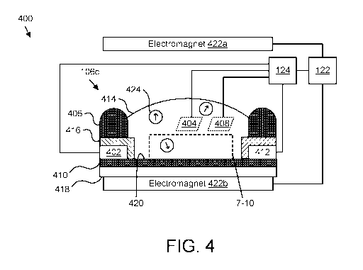
[0097] Figures 4 and 5 are schematic block diagrams illustrating further
embodiments of apparatuses 400, 500 for transportation and detection of
analytes,
including embodiments of beads 424, 524 and bead control components 422, 522.
In
the depicted embodiments, the apparatuses 400, 500 includes a further
embodiment of
a biologically gated transistor 106c, coupled to a bead control device 122 and
a
measurement controller 124. The biologically gated transistor 106c is depicted
in a
CA 03147727 2022-01-14
WO 2021/026458
PCT/US2020/045417
26
cross-section view, from the side. The biologically gated transistor 106c, the
measurement controller 124, the bead control device 122, the bead control
components
422, and the beads 424 in the depicted embodiment may be substantially as
described
above with reference to Figures 1 through 3, and are described further below.
[0098] In the depicted embodiments, the biologically gated transistor 106c
includes a source 412, a drain 402, a channel 410, a reference electrode 408,
a counter
electrode 404, and a liquid well 406, which may be substantially as described
above.
The channel 410, in the depicted embodiment, is a two-dimensional graphene
region
disposed on a substrate 418. The source 412 and drain 402 are formed in
contact with
the channel 410, and are covered by a dielectric 416 (e.g., silicon nitride).
A fluid 414
is applied in contact with the surface 420 of the channel 410, which is the
sensing
surface 420 for a chip-based field effect biosensor 104. For example, the
fluid 414 may
be pipetted (or otherwise inserted) into the liquid well 406 to contact the
sensing surface
420, the reference electrode 408, and the counter electrode 404. The
dielectric 416
electrically insulates the source 412 and drain 402 from the fluid 414, so
that current
between the source 412 and drain 402 is through the channel 410 rather than
directly
through the applied fluid 414.
[0099] The measurement controller 124, in the depicted embodiment, is
coupled to the source 412, the drain 402, the reference electrode 408, and the
counter
electrode 404. In various embodiments, the measurement controller 124 may
apply
excitation conditions to the biologically gated transistor 106c via the source
412, the
drain 402, and/or the counter electrode 404. In further embodiments, the
measurement
controller 124 may perform measurements of one or more output signals from the
biologically gated transistor 106c via the source 412, the drain 402, and/or
the reference
electrode 408.
[0100] In the depicted embodiments, the fluid 414 includes a plurality of
beads
424, 524 that can be electromagnetically positioned within the fluid 414 by
bead control
components 422, 522. Capture moieties and target moieties are not shown in
Figures
4 and 5 so as to more clearly depict other aspects of the beads 424, 524, and
bead control
components 422, 522, but are described in further detail below with reference
to Figure
6.
[0101] In one embodiment, as depicted in Figure 4, beads 424 are magnetic.
Arrows on the beads 424 in Figure 4 indicate the orientation of magnetic
dipoles for
the beads 424. Additionally, in the depicted embodiment, the bead control
device 122
includes or is coupled to bead control components 422, which in the depicted
CA 03147727 2022-01-14
WO 2021/026458
PCT/US2020/045417
27
embodiment are electromagnets 422a, 422b. As shown in Figure 4, the bead
control
device 122 is not powering either of the electromagnets 422, and the beads 424
are not
necessarily oriented to any particular magnetic field. For example, the
magnetic
interaction of the beads 424 with the earth's magnetic field may be weaker
than other
forces within the fluid 414. However, if the bead control device 122 turns on
either
electromagnet 422, the beads 424 will be oriented to the applied magnetic
field, and
attracted to the powered-up electromagnet 422.
[0102] With magnetic beads 424, the bead control components 422 may include
a first electromagnet 422b positioned to move the beads in a first direction
toward the
sensing surface 420 and a second electromagnet 422a positioned to move the
beads in
a second direction away from the sensing surface 420. For example, in the
depicted
embodiment, electromagnet 422b is positioned under the sensing surface 420,
and can
be controlled to position beads 424 within the measurement distance of the
sensing
surface 420, by moving beads toward the sensing surface 420 or holding them in
position. Conversely, electromagnet 422a, is positioned above the fluid 414,
and can
be controlled to position beads 424 further than the measurement distance of
the sensing
surface 420. For example, depending on the strength of the magnetic
interaction
between the electromagnet 422a and the beads 424 relative to the surface
tension of the
fluid 414, the electromagnet 422 may attract the beads 424 towards the upper
surface
of the fluid 414, away from the sensing surface 420, or may entirely remove
the beads
424 from the fluid 414 (e.g., so that beads that have not been incubated in a
sample
solution can be replaced by incubated beads).
[0103] In another embodiment, as depicted in Figure 5, beads 524 are
electrically charged. A plus sign on the beads 524 in Figure 5 indicate that
the beads
have a positive electric charge. However, beads in another embodiment may have
a
negative charge. Additionally, in the depicted embodiment, the bead control
device 122
includes or is coupled to one or more bead control components 522. With
charged
beads 524, the bead control device 122 controls an electric field to move the
beads 524.
For example, in the depicted embodiment, the bead control device 122 applies
an
electric field using field plates 522a, 522b. The bead control device 122 may
apply a
voltage difference across field plates 522a and 522b so that the resulting
electric field
moves or positions the beads 524. Field plates 522, in various embodiments,
may be
any conductors to which a potential may be applied so that the potential
gradient results
in an electric field. For example, in the depicted embodiment, the field
plates 522 are
conductors above and below the biologically gated transistor 106c. In another
CA 03147727 2022-01-14
WO 2021/026458
PCT/US2020/045417
28
embodiment, however, conductors within the biologically gated transistor 106c
may be
used to move or position electrically charged beads 524. For example, a
potential
applied to the channel 410 or to the substrate 418 beneath the channel may be
used to
attract or repel beads 524 toward or away from the surface 420. Thus, the
channel 410
or substrate 418 may be used as a bead control component 522 to produce an
electric
field that moves beads 524.
[0104] Figure 6 is a diagram illustrating beads 624, in one embodiment. In the
depicted embodiment, beads 624 may be magnetic beads substantially similar to
the
magnetic beads 424 described above with reference to Figure 4, or may be
electrically
charged beads substantially similar to the charged beads 524 described above
with
reference to Figure 5. Beads 624, in various embodiments, may be
functionalized with
a capture moiety 626, to bind to a target moiety. Various capture moieties are
described
herein, and are represented in Figure 6 as lines extending from the surface of
the beads
624. Figure 6 depicts two beads 624 functionalized with capture moieties 626,
where
a first bead 624a has not been incubated with an analyte, and where the second
bead
624b has been incubated in a solution containing the analyte 628, so that one
or more
of the capture moieties 626 of bead 624b has bound to a target moiety of the
analyte
628. In some embodiments, a target moiety may be a known moiety of an analyte
628,
either because the target moiety is naturally present as a component of the
analyte 628,
or because the sample solution 110 has been pre-treated to bind the target
moiety to the
analyte 628. In the depicted embodiment, the analyte 628 is DNA, and the
target moiety
may be a particular sequence of nucleotides, a biotin molecule that has been
linked to
the DNA molecule, or the like. Various other types of analytes 628 and
corresponding
target moieties may be bound to by various capture moieties 626.
[0105] A capture moiety 626, in various embodiments, may be any moiety with
an affinity for binding to a target moiety. Beads 624 with a particular
capture moiety
626 may be selected for transport of an analyte 628 in an apparatus or system,
based on
a known target moiety of the analyte 628. In various embodiments, a capture
moiety
626 may include antibodies, a biotin-binding protein (e.g., streptavidin,
neutravidin,
avidin, captavidin, or the like), biotin, zinc finger proteins or CRISPR Cos
family
enzymes, nucleic acids or the like. Certain capture moieties 626 may bind
certain
corresponding target moieties. For example, antibodies may bind to antigens,
biotin-
binding proteins may bind to biotin, and zinc finger proteins or CRISPR Cos
family
enzymes may bind to nucleic acids. Various other or further capture moieties
626 may
be used to bind other or further target moieties. Capture moieties 626 may be
CA 03147727 2022-01-14
WO 2021/026458
PCT/US2020/045417
29
functionalized to beads 624 by binding or linking the capture moieties to the
surface of
the beads 624. Various beads 624 functionalized with different capture
moieties 626
may be commercially available.
[0106] Figures 7-10 are detail views of a region outlined in dashed lines in
Figure 4. The depicted region is above the sensing surface 420 of a chip-based
field
effect biosensor 104 (e.g., the surface of a channel 410 for a biologically
gated transistor
106, or a working electrode surface for a capacitive electrochemical sensor).
The
applied fluid 414 above the sensing surface is depicted, with beads 624 as
described
above with reference to Figures 4-6 (e.g., magnetic beads or electrically
charged beads).
The same region is depicted at successive points in a measurement or analysis
process
in successive Figures 7-10. Capture moieties 626 depicted as lines in Figure 6
are not
depicted in Figures 7-10 for convenience in depicting other aspects of
measurement or
analysis process. Nevertheless, the beads 624 as depicted in Figures 7-10 are
functionalized with a capture moiety 626 as described above. A dashed line
indicates
the measurement distance 730, so that beads 624 that are at least partially
below the
dashed line are within the measurement distance 730 of the sensing surface
420, and
beads 624 that are fully above the dashed line are not within the measurement
distance
730. In Figures 7-10, as in Figure 6, the reference number 624a is used to
indicate
beads 624 where capture moieties are not bound to target moieties, and the
reference
number 624b is used to indicate beads 624 where capture moieties are bound to
target
moieties, so that the beads 624b are bound to analytes 628
[0107] Figure 7 depicts a first set of beads 624, during a calibration
measurement. The measurement controller 124 operates the bead control device
122
to position the beads 624 within the measurement distance 730 of the sensing
surface
420. The first set of beads 624 has not been incubated in a sample solution
110, and
thus the beads 624 not been exposed to or bound to the analyte 628.
[0108] In the depicted embodiment, the quantity of beads 624 in the first set
of
beads is sufficient to form a single layer of beads within the measurement
distance 730,
during the calibration measurement. In another embodiment, the quantity of
beads 624
may form a partial layer of beads 624 within the measurement distance 730,
leaving
some of the sensing surface 420 uncovered by beads 624. In another embodiment,
the
quantity of beads quantity of beads 624 in the first set of beads is
sufficient to form
multiple layers of beads above the sensing surface 420. One or more layers may
be
within the measurement distance 730. For example, if the diameter of the beads
624 is
CA 03147727 2022-01-14
WO 2021/026458
PCT/US2020/045417
approximately half of the measurement distance 730, two layers of beads 624
may stack
up within the measurement distance.
[0109] To perform the calibration measurement, the measurement controller
124 uses excitation circuitry to apply excitation conditions to the biosensor
104, and
5 uses
measurement circuitry to measure one or more of the output signals from the
biosensor 104 that are affected by charges within the measurement distance
730.
Because the first set of beads 624 have not been incubated in the sample
solution, the
calibration measurement allows the measurement controller 124 to measure and
record
output signals that are not affected by the analyte, for later comparison to
output signals
10 that may have been affected by the analyte.
[0110] Figure 8 depicts the first set of beads 624 removed from the sensing
surface 420. The measurement controller 124 operates the bead control device
122 to
move the beads 624 away from the sensing surface 420. For example, the bead
control
device 122 may operate an electromagnet 422a to attract magnetic beads away
from the
15 sensing
surface 420, or may control an electric field to move charged beads away from
the sensing surface 420. Although Figure 8 depicts the beads 624 at the top of
the
depicted region to indicate that they have been removed from the sensing
surface 420,
actual beads 624 removed from a sensing surface 420 may be moved out of the
depicted
region, dispersed throughout the bulk of the fluid 414, positioned at a
particular location
20 within the
fluid 414 away from the sensing surface 420, removed from the fluid 414, or
the like. In various embodiments, removing the first set of beads 624 from the
sensing
surface 420 after the calibration measurement clears the sensing surface 420
for
subsequent measurements using a second set of beads 624.
[0111] Figure 9 depicts incubation of a second set of beads 624 in a sample
25 solution
110. The sample solution 110 may contain an analyte 628 to be detected, or
the analyte may not be present in the sample solution 110 (in which case the
assay may
determine that the analyte 628 is absent). Incubation of beads 624 in the
sample
solution allows the capture moiety 626 of the beads to bind to the target
moiety of the
analyte, if the analyte is in fact present in the sample solution 110.
30 [0112] In
various embodiments, the second set of beads 624, which are
incubated in the sample solution 110, may be the same set of beads as the
first set of
beads 624 used for the calibration measurement, or may be a different set of
beads. In
the depicted embodiment, the second set of beads is the same as the first set
of beads.
The second set in this embodiment is formed by incubating the first set of
beads in the
sample solution 110. For example, the first set of beads may be removed from
the fluid
CA 03147727 2022-01-14
WO 2021/026458
PCT/US2020/045417
31
414 applied to the sensing surface 420 and separately incubated in the sample
solution.
Alternatively, as depicted in Figure 9, the beads 624 may be incubated in situ
by adding
the sample solution 110 to the applied fluid 414, or by exchanging the sample
solution
110 with the applied fluid 414. Bead control components 422, 522 may be used
to hold
beads in place during fluid exchange so that the beads 624 are not removed
from the
biosensor 104.
[0113] In another embodiment, the second set of beads 624 may be a different
set of beads from the first set, and may be formed by incubating beads
separate from
the first set of beads in the sample solution 110. For example, the first set
and the
second set of beads 624 may respectively be different sets of non-incubated
and
incubated beads 624. The incubation of a separate set of beads in the sample
solution
110 may take place with the sample solution 110 separate from the fluid 414
(e.g., in a
separate container). The second set of beads 624 may subsequently be removed
from
the sample solution 110 prior to adding them to the fluid 414 applied to the
sensing
surface 420. In such a case, the first set of beads 624 may have been fully
removed
from the fluid 414 so as not to interfere with measurements involving the
second set of
beads 624. Incubating a second set of beads in the sample solution 110 where
the
second set is separate from the first set allows the incubation to take place
before or
during the calibration measurement (which uses the first set).
[0114] In the incubation stage, if the analyte 628 is present in the sample
solution 110, the surface of the beads 624 may be exposed to the analyte, so
that the
capture moiety 626 of the beads 624 binds to the target moiety of the analyte
628. Thus,
Figure 9 depicts some beads 624a that have not yet bound to the analyte 628
and other
beads 624b that are bound to the analyte 628. In certain embodiments, the
beads in the
second set of beads 624 may collectively have a greater surface area than the
sensing
surface 420. Additionally, as the beads move within the sample solution 110,
the
analyte 628 (if present) may contact the surface of the beads 624 more
frequently than
it contacts the sensing surface 420. Thus, functionalizing beads 624 with a
capture
moiety 626 instead of functionalizing the sensing surface 420 with the capture
moiety
626 may provide more opportunities to bind the analyte to a surface for
eventual
detection. Additionally, beads 624 functionalized with a capture moiety 626
may be
used with a bare or unfunctionalized sensing surface 420, allowing for
multiple assays
involving different capture moieties to be performed without requiring
multiple types
of biosensors 104.
CA 03147727 2022-01-14
WO 2021/026458
PCT/US2020/045417
32
[0115] In certain embodiments, the beads 624 may be washed after incubation,
and prior to performing the detection measurement described below with
reference to
Figure 10. Washing the beads 624 may remove ions, molecules, or moieties that
are
not bound to the beads by the capture moieties 626, effectively purifying any
analyte
628 bound to the beads 624, for subsequent detection. The beads may be washed
in a
fluid similar or identical to the fluid 414 initially applied to the biosensor
for the
calibration measurement. For example, the fluid 414 may be a buffer solution,
purified
water, or the like. Where the beads were incubated in situ by adding the
sample solution
110 to the fluid, washing may include using bead control components 422, 522
may be
used to hold beads in place during fluid exchange with new fluid 414. Where
the beads
were incubated in a separate container, washing may similarly involve
magnetically or
electrically securing the beads 624 so they are not washed away, while rinsing
the
sample solution 110 away from the beads 624.
[0116] Figure 10 depicts the second set of beads 624 during a detection
measurement. In the depicted embodiment, the analyte 628 was present in the
sample
solution, and is bound to at least some of the beads 624b. The measurement
controller
124 operates the bead control device 122 to position the beads 624 within the
measurement distance 730 of the sensing surface 420. Because the second set of
beads
624 has been incubated in the sample solution 110, the analyte 628 is bound to
at least
some of the beads 624b. Thus, bringing the second set of beads within the
measurement
distance 730 also brings at least some of the analyte 628 within the
measurement
distance 730 of the sensing surface 420. (Conversely, if the analyte was not
present in
the sample solution 110, the beads will not be bound to analyte 628, and the
detection
measurement will be similar to the calibration measurement).
[0117] The quantity of beads 624 in the second set may be similar to the
quantity in the first set, to form a single layer of beads, a partial layer of
beads, or
multiple layers of beads within the measurement distance, as described above
with
reference to the calibration measurement.
[0118] To perform the detection measurement, the measurement controller 124
uses excitation circuitry to apply excitation conditions to the biosensor 104,
and uses
measurement circuitry to measure one or more of the output signals from the
biosensor
104 that are affected by charges within the measurement distance 730. Thus,
with
similar or equivalent quantities of beads 624 in the first set and the second
set, and with
similar or equivalent fluid 414, differences in one or more output signals
between the
calibration and the detection measurements may be caused by the analyte 628,
if
CA 03147727 2022-01-14
WO 2021/026458
PCT/US2020/045417
33
present. Greater differences between the calibration and the detection
measurements
may correspond to greater amounts of the analyte 628.
[0119] Thus, in certain embodiments, the analysis module 116 may determine
a parameter relating to presence of the target moiety in the sample solution
110, based
on the calibration measurement and the detection measurement. For example, a
parameter relating to presence of the target moiety may be an indicator of the
presence,
absence, quantity, or concentration of the target moiety, or of the analyte
containing the
target moiety.
[0120] Figure 11 is a schematic block diagram illustrating one embodiment of
an apparatus 1100 for transportation and detection of analytes, including
embodiments
of a bead control device 122 and a measurement controller 124, which may be
substantially as described above. The bead control device 122 in the depicted
embodiment includes or is in communication with one or more bead control
components such as electromagnets 422 or field plates 522. In the depicted
embodiment, the bead control includes attraction circuitry 1102 and removal
circuitry
1104.
[0121] Attraction circuitry 1102, in various embodiments, includes power
circuitry and/or control circuitry (e.g., including a processor for computer
control) to
power and operate the bead control components to position beads 624 within a
measurement distance 730 of a sensing surface 420. The attraction circuity
1102 may
be operated for calibration measurements and detection measurements to
position non-
incubated and incubated beads, respectively, within the measurement distance.
[0122] Removal circuitry 1104, in various embodiments, includes power
circuitry and/or control circuitry (e.g., including a processor for computer
control) to
power and operate the bead control components to remove beads from a sensing
surface
420. The removal circuity 1104 may be operated between a calibration
measurement
and a detection measurement, allowing the non-incubated beads to be removed
from
the sensing surface 420 prior to sensing of incubated beads. The measurement
controller 124 may communicate with the bead control device 122, including
attraction
circuitry 1102 and/or removal circuitry 1104, to position beads during and
between
calibration and detection measurements.
[0123] The measurement controller 124, in the depicted embodiment, includes
excitation circuitry 1106 and measurement circuitry 1108. Certain components
indicated by dashed lines in Figure 11 are included in the depicted
embodiment, but
may be omitted in another embodiment. In the depicted embodiment, the
measurement
CA 03147727 2022-01-14
WO 2021/026458
PCT/US2020/045417
34
controller 124 includes an analysis module 116, communication circuitry 1110,
temperature control circuitry 1112, and a fluidic device 1114. The measurement
controller 124 and analysis module 116 in the depicted embodiment may be
substantially as described above with reference to previous Figures.
[0124] In various embodiments, the measurement controller 124 may use
excitation circuitry 1106 to apply excitation conditions to a chip-based field
effect
biosensor 104 that includes a sensing surface, and may use measurement
circuitry 1108
to perform one or more measurements of at least one of the one or more output
signals
from the chip-based field effect biosensor 104. The output signal(s) may be
affected
by the excitation conditions, and by charges within a measurement distance of
the
sensing surface.
[0125] In some embodiments, the measurement controller 124 may include an
analysis module 116 to determine a parameter relating to presence of a target
moiety in
a sample solution 110, based on the one or more measurements from the
measurement
circuitry 1108. In some embodiments, however, the measurement controller 124
may
not include an analysis module 116. For example, in one embodiment an analysis
module 116 may be implemented by a computing device 114 separate from the
measurement controller 124. In some embodiments, the measurement controller
124
may include communication circuitry 1110 to transmit the measurements from the
measurement circuitry 1108, or information based on the measurements, to a
remote
data repository 118.
[0126] The excitation circuitry 1106, in the depicted embodiment, is
configured
to apply one or more excitation conditions to a chip-based field effect
biosensor 104,
or a set of chip-based field effect biosensors 104. An excitation condition,
in various
embodiments, may be a physical, chemical, or electrical condition applied to
biologically gated transistor 106, such as a voltage, amplitude, frequency,
amplitude,
phase, or waveform for an electrical or electrochemical excitation, a
temperature, a fluid
flow rate, or the like. Excitation circuitry 1106 may be any circuitry that
applies,
modifies, removes, or otherwise controls one or more excitation conditions.
[0127] In some embodiments, excitation conditions may include one or more
electrical signals applied to a chip-based field effect biosensor 104 (or
electrochemical
potentials applied to the fluid in contact with the biosensor), such as
constant-voltage
biases or time-varying excitation signals. Excitation circuitry 1106 may
produce biases
or other excitation signals or couple them to the chip-based field effect
biosensor 104
(e.g., via a source 212, drain 202, or counter electrode 204). Accordingly, in
various
CA 03147727 2022-01-14
WO 2021/026458
PCT/US2020/045417
embodiments, excitation circuitry 1106 may include any circuitry capable of
generating
or modulating biases or excitation signals, such as power supplies, voltage
sources,
current sources, oscillators, amplifiers, function generators, bias tees
(e.g., to add a DC
offset to an oscillating waveform), a processor executing code to control
input/output
5 pins, signal generation portions of source measure units, lock-in
amplifiers, network
analyzers, chemical impedance analyzers, or the like. Excitation circuitry
1106 in
various other or further embodiments may include various other or further
circuitry for
creating and applying programmable biases.
[0128] In some embodiments, excitation conditions may include a temperature
10 for the fluid applied to a chip-based field effect biosensor 104, and
excitation circuitry
1106 may use temperature control circuitry 1112 to control the temperature.
Controlling
the temperature, in various embodiments, may include increasing or decreasing
the
temperature (e.g., to detect or analyze temperature-sensitive aspects of a
biochemical
interaction) maintaining a temperature in a range or near a target
temperature,
15 monitoring temperature for feedback-based control, or the like. Thus,
temperature
control circuitry 1112 may include any circuitry capable of changing the
temperature
of the fluid and/or the chip-based field effect biosensor 104. For example, in
various
embodiments, temperature control circuitry 1112 may include a resistive
heater, a Joule
heating controller to control current in a resistive heater (or in the channel
210 itself), a
20 solid-state heat pump, a thermistor, or the like. Temperature control
circuitry 1112 in
various other or further embodiments may include various other or further
circuitry for
controlling or measuring a temperature.
[0129] Additionally, in some embodiments, excitation circuitry 1106 may
include other or further circuitry for applying excitation conditions other
than or in
25 addition to electrical signals and/or temperature. For example,
excitation circuitry 1106
may include electromagnets for magnetic excitation, light emitters of any
desired
wavelength, radioactive sources, emitters of ultraviolet light, x-rays, gamma
rays,
electron beams, or the like, ultrasonic transducers, mechanical agitators, or
the like.
Various other or further types of excitation circuitry 1106 may be used to
apply various
30 other or further excitation conditions.
[0130] As described above, one or more output signals for a chip-based field
effect biosensor 104 may be affected by or sensitive to charges within the
measurement
distance of the sensing surface. As a simple example, with excitation
conditions that
include a constant drain-to-source bias voltage, charges within the
measurement
35 distance may affect an output signal, such as a drain-to-source current,
a capacitance of
CA 03147727 2022-01-14
WO 2021/026458
PCT/US2020/045417
36
an ionic double layer formed at the sensing surface 420 (e.g., as measured
between the
drain 202 and the reference electrode 208), or the like. Various output
signals that may
be affected by charges within the measurement distance, and measured, may
include a
complex resistance (e.g., impedance) of a channel 210 for a biologically gated
transistor
106, electrical current through the channel 210, voltage drop across the
channel 210,
coupling between the channel 210 and the liquid gate (e.g., biased and/or
measured via
a counter electrode 204 and/or a reference electrode 208), electrical
(channel) and/or
electrochemical (liquid gate) voltages, currents, resistances, capacitances,
inductances,
complex impedances, network parameters (e.g., S-parameters or h-parameters
determined using a network analyzer), a Dirac voltage (e.g., a liquid gate
voltage that
minimizes channel current in a graphene channel 210), charge carrier mobility,
contact
resistance, kinetic inductance, a spectrum based on multiple measurements such
as a
power spectral density, an electrical impedance spectrum, an electrochemical
impedance spectrum, or the like.
[0131] Measurement circuitry 1108, in various embodiments, may include any
circuitry capable of performing measurements of one or more output signals.
For
example, in some embodiments, measurement circuitry 1108 may include
preamplifiers, amplifiers, filters, voltage followers, data acquisition (DAQ)
devices or
boards, sensor or transducer circuitry, signal conditioning circuitry, an
analog-to-digital
converter, a processor executing code to receive and process signals via
input/output
pins, measurement portions of source measure units, lock-in amplifiers,
network
analyzers, chemical impedance analyzers, or the like. Measurement circuitry
1108 in
various other or further embodiments may include various other or further
circuitry for
performing measurements of output signals.
[0132] In various embodiments, portions or components of excitation circuitry
1106 and/or measurement circuitry 1108 may be disposed in a chip-based field
effect
biosensor 104, a chip reader device 102, or in a separate device (e.g., lab
bench test and
measurement equipment) coupled to the chip-based field effect biosensor 104.
For
example, single-use components such as a resistive heater component for
excitation
circuitry 1106 may be disposed on a chip-based field effect biosensor 104,
while multi-
use components such a digital signal processing circuitry for generating or
analyzing
complex waveforms may be disposed in a chip reader device 102. Various other
ways
to dispose or arrange portions or components of excitation circuitry 1106
and/or
measurement circuitry 1108 may be used in various other embodiments.
CA 03147727 2022-01-14
WO 2021/026458
PCT/US2020/045417
37
[0133] The analysis module 116, in some embodiments, is configured to
determine a parameter relating to presence of the target moiety, based on the
calibration
and detection measurements performed by the measurement circuitry 1108. Such a
parameter may include an indication of whether or not the target moiety is
present in
the sample solution 110, a concentration of the target moiety or another
parameter
corresponding to or related to the concentration, or the like. In various
embodiments,
an analysis module 116 may use various methods, including known quantitative
analysis methods to determine a parameter relating to presence of the target
moiety,
based on the calibration and detection measurements. Results from the analysis
module
116, such as parameters characterized by the analysis module 116, may be
communicated to a user directly via a display or printout (e.g., from the chip
reader
device 102), transmitted to a user via data network 120, saved to a storage
medium
(e.g., in remote data repository 118) for later access by one or more users,
or the like.
[0134] In some embodiments, an analysis module 116 may be separate from the
measurement controller 124. For example, an analysis module 116 may be
implemented by a computing device 114 separate from the measurement controller
124.
Thus, in some embodiments, a measurement controller 124 may include
communication circuitry 1110, instead of or in addition to an analysis module
116.
Communication circuitry 1110, in the depicted embodiment, is configured to
transmit
information to a remote data repository 118. The communication circuitry 1110
may
transmit information via the data network 120, and may include components for
data
transmission (and possibly reception), such as a network interface controller
(NIC) for
communicating over an ethernet or Wi-Fi network, a transceiver for
communicating
over a mobile data network, or the like. Various other or further components
for
transmitting data may be included in communication circuitry 1110 in various
other or
further embodiments.
[0135] In some embodiments, the information transmitted by the
communication circuitry 1110 to the remote data repository 118 may be
information
based on the measurements performed by the measurement circuitry 1108.
Information
based on the measurements may be the measurements themselves (e.g., raw
samples),
calculated information based on the measurements (e.g., spectra calculated
from the
raw data), and/or analysis results (e.g., a determined parameter) from the
analysis
module 116. In a further embodiment, an analysis module 116 may be in
communication with the remote data repository 118 (e.g., via the data network
120).
An analysis module 116 may be configured to characterize one or more
parameters
CA 03147727 2022-01-14
WO 2021/026458
PCT/US2020/045417
38
based on the information transmitted to the remote data repository 118. For
example,
instead of the analysis module 116 receiving measurements directly from the
measurement circuitry 1108, the communication circuitry 1110 may transmit
measurements (or information about the measurements) to the remote data
repository
118, and the analysis module 116 may retrieve the measurements (or information
about
the measurements) from the remote data repository 118.
[0136] In some embodiments, storing data in a remote data repository 118 may
allow information to be aggregated from multiple measurement controllers 124
for
remote analysis of phenomena that may not be apparent from a single
measurement
controller 124. For example, for epidemiology purposes, a measurement
controller 124
may determine whether a person is infected with a disease based on one or more
analytes such as viruses, antibodies, DNA or RNA from a pathogen, or the like,
in a
sample obtained from the person, which may include a sample of blood, saliva,
mucus,
cerebrospinal fluid, stool, or the like. Information uploaded to a remote data
repository
118 from multiple measurement controllers 124 may be used to determine
aggregate
characteristics, such as how infection rates differ in different geographical
regions. In
various embodiments, an analysis module 116 may implement various other or
further
ways of using aggregate information from multiple measurement controllers 124
[0137] The measurement controller 124, in various embodiments, may use
excitation circuitry 1106, measurement circuitry 1108, and an analysis module
116
together in various ways with one or more chip-based field-effect biosensors
104 to
determine or characterize parameters relating to presence of a target. In some
embodiments, multiple chip-based field-effect biosensors 104 may be
homogeneously
configured (e.g., for redundancy) or heterogeneously configured (e.g., with
sensing
surfaces 420 functionalized in different ways to characterize different
aspects of a
biochemical interaction).
[0138] The fluidic device 1114, in various embodiments, may be a device used
by the measurement controller 124 to drive flow of a fluid through a flow cell
or other
fluidic or microfluidic channels. For example, in some embodiments the
measurement
controller 124 may use a fluidic device 1114 to apply a fluid 414 to the
sensing surface
for a calibration measurement, to exchange the fluid for a sample solution for
incubation of beads 624 between the calibration and detection measurements,
and/or to
drive flow additional fluid 414 after incubation, to remove the sample
solution and wash
the beads 624.
CA 03147727 2022-01-14
WO 2021/026458
PCT/US2020/045417
39
[0139] Figure 12 is a schematic flow chart diagram illustrating one embodiment
of a method 1200 or transportation and detection of analytes. The method 1200
begins
with providing 1202 a plurality of beads 624 functionalized with a capture
moiety 626
to bind to a target moiety. A first set of the beads 624 is positioned 1204
within a fluid
414 to be within a measurement distance 730 of a sensing surface 420 of a chip-
based
field effect biosensor 104. In the depicted embodiment, the first set of the
beads has
not been incubated in a sample solution 110. A calibration measurement is
performed
1206 to measure at least one output signal from the chip-based field effect
biosensor
104. The first set of beads 624 is removed 1208 from the sensing surface 420.
[0140] In some embodiments, the beads 624 may be magnetic, and positioning
1204 the first set of the beads 624 to be within the measurement distance 730
of the
sensing surface 420 includes activating a first electromagnet 422b. Similarly,
removing
1208 the first set of beads 624 from the sensing surface 420 may include
activating a
second electromagnet 422a.
[0141] In some embodiments, the beads 624 may be electrically charged, and
positioning 1204 the first set of the beads 624 to be within the measurement
distance
730 of the sensing surface 420 includes applying a first electric field (e.g.,
by applying
a voltage difference across two conductors such as field plates 522).
Similarly,
removing 1208 the first set of beads 624 from the sensing surface 420 may
include
applying a second electric field (e.g., by changing the voltage of one or more
conductors).
[0142] A second set of beads 624 is incubated 1210 in the sample solution 110.
The second set of beads 624 is positioned 1212 within the fluid 414 to be
within the
measurement distance 730 of the sensing surface 420. A detection measurement
is
performed 1214 to measure at least one output signal. A parameter relating to
presence
of the target moiety in the sample solution 110 is determined 1216, based on
the
calibration measurement and the detection measurement, and the method 1200
ends.
[0143] Figure 13 is a schematic flow chart diagram illustrating another
embodiment of a method 1300 for transportation and detection of analytes.
Certain
steps of the method 1300 may be substantially similar to steps of the method
1200
described above with reference to Figure 12, but other steps may differ.
[0144] The method 1300 begins with providing 1302 a plurality of beads 624
functionalized with a capture moiety 626 to bind to a target moiety. A first
set of the
beads 624 is positioned 1304 within a fluid 414 to be within a measurement
distance
730 of a sensing surface 420 of a chip-based field effect biosensor 104. In
the depicted
CA 03147727 2022-01-14
WO 2021/026458
PCT/US2020/045417
embodiment, the first set of the beads has not been incubated in a sample
solution 110.
A calibration measurement is performed 1306 to measure at least one output
signal
from the chip-based field effect biosensor 104. The first set of beads 624 is
removed
1308 from the sensing surface 420, and from the fluid 414.
5 [0145] A
second set of beads 624 is incubated 1310 in the sample solution 110.
The second set of beads is removed 1312 from the sample solution, washed, and
added
to the fluid 414. The second set of beads 624 is positioned 1314 within the
fluid 414
to be within the measurement distance 730 of the sensing surface 420. A
detection
measurement is performed 1316 to measure at least one output signal. A
parameter
10 relating to
presence of the target moiety in the sample solution 110 is determined 1318,
based on the calibration measurement and the detection measurement, and the
method
1300 ends.
[0146] Figure 14 is a schematic flow chart diagram illustrating another
embodiment of a method 1400 for transportation and detection of analytes.
Certain
15 steps of the
method 1400 may be substantially similar to steps of the method 1200
described above with reference to Figure 12, but other steps may differ.
[0147] The method 1400 begins with providing 1402 a plurality of beads 624
functionalized with a capture moiety 626 to bind to a target moiety. A first
set of the
beads 624 is positioned 1404 within a fluid 414 to be within a measurement
distance
20 730 of a
sensing surface 420 of a chip-based field effect biosensor 104. In the
depicted
embodiment, the first set of the beads has not been incubated in a sample
solution 110.
A calibration measurement is performed 1406 to measure at least one output
signal
from the chip-based field effect biosensor 104. The first set of beads 624 is
removed
1408 from the sensing surface 420, and from the fluid 414.
25 [0148] A
second set of beads 624 is incubated 1410 in the sample solution 110,
by adding the sample solution 110 to the fluid 414. The second set of beads is
washed
1412 by securing the beads (e.g., using bead control components) while
exchanging the
fluid that has been mixed with the sample solution 110 for new fluid 414 that
has not
been mixed with the sample solution 110. The second set of beads 624 is
positioned
30 1414 within
the fluid 414 to be within the measurement distance 730 of the sensing
surface 420. A detection measurement is performed 1416 to measure at least one
output
signal. A parameter relating to presence of the target moiety in the sample
solution 110
is determined 1418, based on the calibration measurement and the detection
measurement, and the method 1400 ends.
CA 03147727 2022-01-14
WO 2021/026458
PCT/US2020/045417
41
[0149] A means for positioning a plurality of beads 624 within a fluid 414,
within a measurement distance within a measurement distance 730 of a sensing
surface
430 of a chip-based field effect biosensor 104, in various embodiments, may
include a
bead control device 122, one or more bead control components, one or more
electromagnets 422, one or more field plates or other conductors, or other
means
disclosed herein. Other embodiments may include similar or equivalent means
for
positioning beads 624.
[0150] A means for performing a calibration measurement, in various
embodiments, may include a measurement controller 124, excitation circuitry
1106,
measurement circuitry 1108, or other means disclosed herein. Other embodiments
may
include similar or equivalent means for performing a calibration measurement.
[0151] A means for performing a detection measurement, in various
embodiments, may include a measurement controller 124, excitation circuitry
1106,
measurement circuitry 1108, or other means disclosed herein. Other embodiments
may
include similar or equivalent means for performing a detection measurement.
[0152] A means for removing beads 624 from a sensing surface 420 between a
calibration measurement and a detection measurement, in various embodiments,
may
include a bead control device 122, one or more bead control components, one or
more
electromagnets 422, one or more field plates or other conductors, or other
means
disclosed herein. Other embodiments may include similar or equivalent means
for
removing beads 624.
[0153] A means for determining a parameter relating to presence of a target
moiety in a sample solution 110, based on a calibration measurement and a
detection
measurement, in various embodiments, may include an analysis module 116, a
processor executing machine-readable code with instructions for determining
the
parameter, other logic hardware or executable code, or other means disclosed
herein.
Other embodiments may include similar or equivalent means for determining a
parameter.
[0154] Embodiments may be practiced in other specific forms. The described
embodiments are to be considered in all respects only as illustrative and not
restrictive.
The scope of the invention is, therefore, indicated by the appended claims
rather than
by the foregoing description. All changes which come within the meaning and
range of
equivalency of the claims are to be embraced within their scope.