Note: Descriptions are shown in the official language in which they were submitted.
MEMS STRAIN GAUGE PRESSURE SENSOR WITH MECHANICAL SYMMETRIES
BACKGROUND
[0001] This disclosure relates generally to pressure sensors, and more
specifically to
microelectromechanical system (MEMS) strain gauge pressure sensors.
[0002] MEMS pressure sensors are configured to measure the pressure of a
fluid. Pressure
sensors can be absolute pressure sensors that measure a pressure of a first
fluid compared to a
reference pressure (typically a vacuum). Pressure sensors can also be
differential pressure sensors
that measure a difference in pressure between a first fluid and a second
fluid. Pressure sensors can
measure pressure in a variety of ways. For example, a MEMS pressure sensor can
include a
diaphragm that deforms or deflects based on the pressure of a first fluid
and/or a second fluid, and
a piezoresistive strain gauge sensor on the diaphragm can measure the strain
in the diaphragm
caused by the deformation of the diaphragm. Pressure sensors can have a first
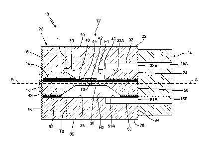
cavity on a first side
of the diaphragm and a second cavity on a second side of the diaphragm. In a
differential pressure
sensor, the first and second cavities can be connected to two separate fluid
sources.
[0003] An integrated mechanical structure is required to support the
pressure sensor
diaphragm. Supporting structures can also function as packaging for pressure
sensors, and
differential pressure sensors can have more complex structures. Strain gauge
pressure sensors are
very sensitive to mechanical stress generated by supporting structures (i.e.,
packaging).
Mechanical stress from the supporting structures can be transferred to the
pressure sensor and
cause the diaphragm to deflect. This will cause an erroneous output in the
pressure sensor, as the
deflection of the diaphragm is not being caused by pressure differences but
rather by stress in the
system.
SUMMARY
[0004] In one example, a microelectromechanical system (MEMS) strain
gauge pressure
sensor includes a top wafer stack having a top surface and a first cavity that
is configured to receive
a first fluid at a first pressure, a backing wafer having a bottom surface
opposite the top surface of
the top wafer stack; a diaphragm wafer positioned between the top wafer stack
and the backing
wafer and having a second cavity that is configured to receive a second fluid
at a second pressure,
1
Date Recue/Date Received 2022-02-08
and a pedestal connected laterally to the top wafer stack, the backing wafer,
and the diaphragm
wafer. The diaphragm wafer includes a diaphragm extending between the first
cavity and the
second cavity and configured to deflect from the first pressure and/or the
second pressure, and a
resistor positioned on the diaphragm to sense a deflection of the diaphragm.
The MEMS strain
gauge pressure sensor has a central axis that is parallel to the top surface
and the bottom surface
such that the MEMS strain gauge pressure sensor has mechanical symmetries
about the central
axis.
[0005] In another example, a method of fabricating a
microelectromechanical system
(MEMS) strain gauge pressure includes forming a top wafer stack having a top
surface and
defining a first cavity, forming a backing wafer having a bottom surface, and
forming a diaphragm
wafer defining a second cavity. The diaphragm wafer includes a diaphragm
configured to deflect
from a difference in pressure, and a resistor positioned on the diaphragm to
sense a deflection of
the diaphragm. The method further includes bonding the top wafer stack to the
diaphragm wafer
and bonding the diaphragm wafer to the backing wafer to form a full wafer
stack, such that the
diaphragm wafer is positioned between the top wafer stack and the backing
wafer, the diaphragm
is positioned between the first cavity and the second cavity, and the top
surface is opposite the
bottom surface. The method further includes attaching a pedestal laterally to
the top wafer stack,
the backing wafer, and the diaphragm wafer. The MEMS strain gauge pressure
sensor has a central
axis that is parallel to the top surface and the bottom surface such that the
MEMS strain gauge
pressure sensor has mechanical symmetries about the central axis.
BRIEF DESCRIPTION OF THE DRAWINGS
[0006] FIG. 1 is a schematic cross-sectional side view of a MEMS strain
gauge pressure
sensor.
[0007] FIG. 2 is a process flow diagram showing steps for fabricating a
full wafer stack.
[0008] FIGS. 3A-3F are schematic cross-sectional side views illustrating
steps for
fabricating a top wafer stack.
[0009] FIGS. 4A-4G are schematic cross-sectional side views illustrating
steps for
fabricating a diaphragm wafer.
[0010] FIG. 4H is a schematic isometric view showing the diaphragm wafer.
2
Date Recue/Date Received 2022-02-08
[0011] FIGS. 5A-5C are schematic cross-sectional side views illustrating
steps for
fabricating a backing wafer.
[0012] FIG. 6A is an exploded schematic cross-sectional side view showing
the full wafer
stack.
[0013] FIG. 6B is a schematic cross-sectional side view of the assembled
full wafer stack.
[0014] FIG. 7 is a process flow diagram showing steps for dicing the full
wafer stack and
assembling individual sensors.
[0015] FIGS. 8A-8C are schematic isometric views illustrating steps for
dicing the full
wafer stack into bars and assembling a sheet.
[0016] FIGS. 9A-9C are schematic isometric views illustrating steps for
connecting
contact pads to the sheet.
[0017] FIG. 10 is a partial schematic cross-sectional view of the sheet
showing a dicing
location.
[0018] FIGS. 11A-11C are schematic isometric views illustrating steps for
attaching
pedestals to the sheet.
[0019] FIGS. 12A-12B are schematic isometric views illustrating steps for
further dicing
the sheet into individual sensors.
DETAILED DESCRIPTION
[0020] In general, the present disclosure describes a
microelectromechanical system
(MEMS) strain gauge pressure sensor with mechanical symmetries and a side-
attached pedestal.
The mechanical symmetries and positioning of the pedestal can alleviate
unbalanced stresses
within the pressure sensor and improve sensing accuracy. Additionally, the
pressure sensor can
have a simple and streamlined construction. The MEMS strain gauge pressure
sensor disclosed
herein, and a corresponding method of fabrication, are described below with
reference to FIGS. 1-
12B.
[0021] FIG. 1 is a schematic cross-sectional side view of MEMS strain
gauge pressure
sensor 10. Pressure sensor 10 includes full wafer stack 12, pedestal 14
(including ports 15A and
15B), insulation layer 16, and contact pad 18. Full wafer stack 12 includes
top wafer stack 20
(including first topping wafer 22 and second topping wafer 24), diaphragm
wafer 26, and backing
wafer 28. Top wafer stack 20 also includes first cavity 30, first channel 32
(including openings
3
Date Recue/Date Received 2022-02-08
33A and 33B), and bonding material (e.g., glass frit) 34. Diaphragm wafer 26
includes diaphragm
36, second cavity 38, first insulation layer 40, resistor 42, contact metal
layer 44, second insulation
layer 46, and third insulation layer 48. Backing wafer 28 includes second
channel 50 (including
openings 51A and 51B) and bonding material (e.g., glass frit) 52. Pressure
sensor 10 has first side
54, second side 56, top side 58, and bottom side 60. Also labeled in FIG. 1
are central axis A, first
topping wafer thickness Ti, backing wafer thickness T2, and diaphragm
thickness T3, first cavity
height H1, and second cavity height H2.
[0022] Full wafer stack 12 includes top wafer stack 20, diaphragm wafer
26, and backing
wafer 28. Diaphragm wafer 26 is positioned between top wafer stack 20 and
backing wafer 28
within full wafer stack 12. Each of top wafer stack 20, diaphragm wafer 26,
and backing wafer 28
can be parallel to each other. In an exemplary embodiment, top wafer stack 20,
diaphragm wafer
26, and backing wafer 28 are square when viewed from the top (i.e., from a
perspective that is
perpendicular to that of FIG. 1). In other exemplary embodiments, top wafer
stack 20, diaphragm
wafer 26, and backing wafer 28 have rounded corners, or can be round, when
viewed from the top.
Top wafer stack 20 includes first topping wafer 22 and second topping wafer
24. First topping
wafer 22 defines top side 58 (i.e., a top surface) of pressure sensor 10,
backing wafer 28 defines
bottom side 60 (i.e., a bottom surface) of pressure sensor 10, and top side 58
is opposite bottom
side 60. First topping wafer 22, second topping wafer 24, diaphragm wafer 26,
and backing wafer
28 each extend from first side 54 to second side 56 in pressure sensor 10.
Each of first topping
wafer 22, second topping wafer 24, diaphragm wafer 26, and backing wafer 28
can be silicon
wafers.
[0023] First topping wafer 22 is bonded to second topping wafer 24. For
example, first
topping wafer 22 can be bonded to second topping wafer 24 by silicon wafer
fusion bonding to
form top wafer stack 20. Top wafer stack 20 is bonded at second topping wafer
24 to diaphragm
wafer 26. Specifically, bonding material 34 is between second topping wafer 24
and diaphragm
wafer 26 to form a bond. In an exemplary embodiment, bonding material 34 is
glass frit, such that
second topping wafer 24 and diaphragm wafer 26 are bonded by glass frit
bonding. In other
exemplary embodiments, bonding material 34 can be any suitable bonding
material, including
metal, polymer, etc. Diaphragm wafer 26 is bonded on an opposite side to
backing wafer 28.
Specifically, bonding material 52 is between diaphragm wafer 26 and backing
wafer 28 to form a
bond. In an exemplary embodiment, bonding material 52 is glass frit, such that
diaphragm wafer
4
Date Recue/Date Received 2022-02-08
26 and backing wafer 28 are bonded by glass frit bonding. In other exemplary
embodiments,
bonding material 52 can be any suitable bonding material, including metal,
polymer, etc. The
thickness of bonding material 34, 52 can be negligible (i.e., the thickness of
bonding material 34,
52 can have no substantial effect on the mechanics of pressure sensor 10).
[0024] Diaphragm 36 is a portion of diaphragm wafer 26 that extends
between first cavity
30 and second cavity 38. Diaphragm 36 has diaphragm thickness T3, as indicated
in FIG. 1.
Diaphragm thickness T3 and an area of diaphragm 36 can define characteristics
of pressure sensor
performance (e.g., range and accuracy). First cavity 30 is a void formed
within top wafer stack 20.
First topping wafer 22, second topping wafer 24, bonding material 34, and
second insulation layer
46 on diaphragm 36 define boundaries of first cavity 30 when pressure sensor
10 is assembled.
The thickness of bonding material 34 (e.g., glass frit) and second insulation
layer 46 in defining
the boundaries of first cavity 30 can be negligible, such that the boundaries
of first cavity 30 are
primarily defined by first topping wafer 22, second topping wafer 24, and
diaphragm 36. Thus,
under vacuum conditions (i.e., the condition shown in FIG. 1, without an
applied system pressure),
first topping wafer 22 is separated from diaphragm 36 by first cavity height
Hl. Second topping
wafer 24 surrounds (i.e., forms a periphery of) first cavity 30. In the
embodiment shown in FIG.
1, second topping wafer 24 has chamfered edges adjacent first cavity 30, such
that first cavity 30
has a trapezoidal cross-sectional area. First cavity 30 can have a uniform
height between the
chamfered edges (e.g., as illustrated by first cavity height H1 in FIG. 1). In
the embodiment shown
in FIG. 1, the chamfered edges of second topping wafer 24 have an angle of
approximately 54.7
degrees (as measured with respect to central axis A). In other embodiments,
first cavity 30 can
have a different cross-sectional shape.
[0025] Second cavity 38 is a void formed within diaphragm wafer 26.
Diaphragm wafer
26 (including diaphragm 36), third insulation layer 48, bonding material 52,
and backing wafer 28
define boundaries of second cavity 38 when pressure sensor 10 is assembled.
The thickness of
bonding material 52 (e.g., glass frit) and third insulation layer 48 in
defining the boundaries of
second cavity 38 can be negligible, such that the boundaries of second cavity
38 are primarily
defined by diaphragm wafer 26 and backing wafer 28. Thus, under vacuum
conditions (i.e., the
condition shown in FIG. 1, without an applied system pressure), backing wafer
28 is separated
from diaphragm 36 by second cavity height H2. Diaphragm wafer 26 surrounds
(i.e., forms a
periphery of) second cavity 38. In the embodiment shown in FIG. 1, diaphragm
wafer 26 has
Date Recue/Date Received 2022-02-08
chamfered edges adjacent second cavity 38, such that second cavity 38 has a
trapezoidal cross-
sectional area. Second cavity 38 can have a uniform height between the
chamfered edges (e.g., as
illustrated by second cavity height H2 in FIG. 1). In the embodiment shown in
FIG. 1, second
cavity height H2 is equal to first cavity height H1 under vacuum conditions
and when a pressure
of a first fluid in first cavity 30 is equal to a pressure of a second fluid
in second cavity 38. In the
embodiment shown in FIG. 1, the chamfered edges of diaphragm wafer 26 have an
angle of
approximately 54.7 degrees (as measured with respect to central axis A). In
other embodiments,
second cavity 38 can have a different cross-sectional shape.
[0026] Resistor 42 is positioned on diaphragm 36 (on first insulation
layer 40, as shown in
FIG. 1) such that resistor 42 is exposed to first cavity 30. Resistor 42 can
be a polysilicon
piezoresistor. The example of FIG. 1 shows a single resistor 42, but it should
be understood that
other embodiments can include multiple resistors 42 arranged on diaphragm 36.
For example, four
resistors 42 can be arranged on diaphragm 36 to form a Wheatstone bridge
circuit. Contact metal
layer 44 contacts resistor 42 and extends across a portion of first insulation
layer 40 to connect to
contact pad 18 at first side 54 of pressure sensor 10, forming an electrical
via (i.e., a contact via).
The number of contact pads 18 can correspond to the number of resistors 42.
[0027] First insulation layer 40 extends across diaphragm wafer 26 on a
first side of
diaphragm wafer 26 that is adjacent first cavity 30. As shown schematically in
FIG. 1, second
insulation layer 46 extends over portions of contact metal layer 44, resistor
42, and first insulation
layer 40. Second insulation layer 46 contacts bonding material 34 of top wafer
stack 20. Third
insulation layer 48 is between diaphragm wafer 26 and bonding material 52 of
backing wafer 28
on a second side of diaphragm wafer 26 that is adjacent second cavity 38.
First insulation layer 40,
second insulation layer 42, and third insulation layer 48 can be any suitable
insulation material.
[0028] Contact metal layer 44 extends between second topping wafer 24 and
diaphragm
wafer 26 to an exterior of pressure sensor 10 at first side 54. Insulation
layer 16 extends across
first side 58 of pressure sensor 10. Insulation layer 16 can be any suitable
insulation material.
Contact pad 18 is positioned on a portion of insulation layer 16 over an end
of contact metal layer
44. Contact pad 18 is an electrical contact material. Contact pad 18 extends
through insulation
layer 16 to contact metal layer 44. Contact pad 18 forms an electrical
connection with contact
metal layer 44 and thereby with resistor 42.
6
Date Recue/Date Received 2022-02-08
[0029] First channel 32 is a channel or trench in first topping wafer 22.
First channel 32
extends between opening 33A and opening 33B. Opening 33A is an opening into
first channel 32
from first cavity 30. Opening 33B is an opening into first channel 32 from an
exterior of pressure
sensor 10 at second side 56. Thus, first channel 32 connects first cavity 30
to an exterior of pressure
sensor 10. First channel 32 can have a rectangular cross-sectional area, as
indicated by dashed lines
in FIG. 1. In other embodiments, first channel 32 can have any suitable cross-
sectional shape.
[0030] In some embodiments, second channel 50 is a channel or trench in
backing wafer
28. Embodiments of pressure sensor 10 including second channel 50 can be
differential pressure
sensors (e.g., as shown in FIG. 1). Embodiments of pressure sensor 10 that do
not include second
channel 50 (or that include a sealed or closed second channel 50) can be
absolute pressure sensors
(not shown). Second channel 50 extends between opening 51A and opening 51B.
Opening 51A is
an opening into second channel 50 from second cavity 38. Opening 51B is an
opening into second
channel 50 from an exterior of pressure sensor 10 at second side 56. Thus,
second channel 50
connects second cavity 38 to an exterior of pressure sensor 10. Second channel
50 can have a
rectangular cross-sectional area, as indicated by dashed lines in FIG. 1. In
other embodiments,
second channel 50 can have any suitable cross-sectional shape.
[0031] Pedestal 14 is connected to second side 56 of pressure sensor 10
and extends
laterally from full wafer stack 12. Pedestal 14 is a support or connecting
structure of pressure
sensor 10 for connecting pressure sensor 10 to other components in a sensing
system. Respective
portions of pedestal 14 can be bonded to first topping wafer 22, second
topping wafer 24,
diaphragm wafer 26, and backing wafer 28. Pedestal 14 can be a solid structure
consisting of two
joined cylindrical portions such that pedestal 14 has a lemniscate-like shape
when viewed from
the side (i.e., from a perspective that is perpendicular to that of FIG. 1).
Ports 15A and 15B extend
through pedestal 14 to second side 56 of pressure sensor 10. Ports 15A and 15B
can communicate
system pressures to an interior of pressure sensor 10. Specifically, port 15A
is aligned with opening
33B of first channel 32 to provide a first fluid to first cavity 30. Port 15B
is aligned with opening
51B of second channel 50 to provide a second fluid to second cavity 38. In an
exemplary
embodiment, pedestal 14 is a glass material that is bonded to full wafer stack
12 at second side 56.
[0032] Pressure sensor 10 has mechanical symmetries about central axis A.
Specifically,
first topping wafer thickness Ti can be equal to backing wafer thickness T2.
Similarly, first cavity
height H1 and second cavity height H2 can be equal under vacuum conditions
(i.e., where there is
7
Date Recue/Date Received 2022-02-08
no deflection of diaphragm 36) and when a pressure of a first fluid in first
cavity 30 is equal to a
pressure of a second fluid in second cavity 38. Diaphragm 36 is symmetric
about central axis A.
In other words, diaphragm thickness T3 is divided in half by central axis A.
Pedestal 14 is also
symmetric about central axis A. As shown in FIG. 1, pedestal 14 has symmetric
attachment to first
topping wafer 22 and backing wafer 28 and to second topping wafer 24 and
diaphragm wafer 26.
Minor asymmetries caused by, e.g., resistor 42, contact metal layer 44, first
channel 32, etc. has a
negligible effect on the mechanics of pressure sensor 10 (i.e., pressure
sensor 10 is mechanically
symmetrical).
[0033] In general, the physical dimensions of pressure sensor 10 can be
different in various
embodiments. More specifically, cavity size (e.g., an area of first cavity 30
and an area of second
cavity 38) and diaphragm thickness (e.g., diaphragm thickness T3) can be
proportional based on
the pressure and desired deflection characteristics of pressure sensor 10.
[0034] In operation, pressure sensor 10 can measure system pressures. In
a differential
pressure sensor embodiment (FIG. 1), first cavity 30 receives a first fluid
(e.g., a gas) at a first
applied pressure via fluid communication with first channel 32. Second cavity
38 receives a second
fluid (e.g., a gas) at a second applied pressure via fluid communication with
second channel 50. A
difference between the first applied pressure and the second applied pressure
causes diaphragm 36
to deflect. Deflection of diaphragm 36 in turn causes a piezoresistive change
in resistor 42. Resistor
42 thereby senses a deflection of diaphragm 36. An electrical circuit (not
shown) applied to contact
pad 18 can be configured to measure this change, thereby providing a
representation of the value
of the applied system pressures (i.e., the difference between the first
applied pressure and the
second applied pressure). Pressure sensor 10 functions similarly in an
absolute pressure sensor
embodiment (not shown), except that second cavity 38 is a vacuum, so there is
no second applied
pressure, and the measured piezoresistive change in resistor 42 therefore
provides a representation
of an absolute (i.e., atmospheric) pressure, rather than a difference between
two applied system
pressures.
[0035] The mechanical symmetry of pressure sensor 10 as described above
can prevent
unbalanced stress from occurring within pressure sensor 10 (e.g., between
first topping wafer 22
and backing wafer 28) and altering the deflection of diaphragm 36.
Additionally, when different
materials are used for the wafers (e.g., silicon) and pedestal 14 (e.g.,
glass), any generated stress
becomes common mode and has a minimal impact on diaphragm 36.
8
Date Recue/Date Received 2022-02-08
[0036] Fabrication of a MEMS strain gauge pressure sensor (e.g., pressure
sensor 10) will
be described with reference to FIGS. 2-12B. In this section, sequential
iterations of work in process
(WIP) features will be indicated with sequential lettering (e.g., "300A,"
"300B," etc.), and WIP
features may be referred to generally by the shared reference number.
[0037] For ease of discussion, FIGS. 2-6B will be described together.
FIG. 2 is a process
flow diagram showing steps of process 200 for fabricating a full wafer stack
(e.g., for MEMS strain
gauge pressure sensor 10 shown in FIG. 1). Process 200 includes sub-processes
210, 212, and 214.
Sub-processes 210, 212, and 214 will be described in turn below.
[0038] Sub-process 210 of process 200 will be described with reference to
FIGS. 3A-3F
below. FIGS. 3A-3F are schematic cross-sectional side views illustrating steps
216-222 of sub-
process 210 of FIG. 2 for fabricating top wafer stack WIP 300. Top wafer stack
WIP 300 and its
component parts are substantially similar in structure to top wafer stack 12
and its component parts
(as described above with reference to FIG. 1), except where in-process
differences are noted. FIG.
3A shows first topping wafer WIP 310. At step 216 of sub-process 210, first
channel 312 is etched
into first topping wafer WIP 310 to form first topping wafer WIP 310A (shown
in FIG. 3B). First
channel 312 is etched into bonding surface 314 away from a periphery of first
topping wafer WIP
310A. FIG. 3C shows second topping wafer WIP 316 with bonding surface 318. At
step 218,
second topping wafer WIP 316 is etched to form chamfered edges 320 of second
topping wafer
WIP 316A (shown in FIG. 3D). In an exemplary embodiment, etching in step 218
can be a full-
thickness KOH etching, and chamfered edges 320 will have angles of
approximately 54.7 degrees.
In other embodiments, etching can be other "dry" or "wet" etch processes known
in the art and
result in different angles of chamfered edges 320 or a different profile
without chamfered edges
320.
[0039] At step 220, first topping wafer WIP 310A (shown in FIG. 3B) and
second topping
wafer WIP 316A (shown in FIG. 3D) are bonded along bonding surfaces 314 and
318 to form top
wafer stack WIP 300 (shown in FIG. 3E). In an exemplary embodiment, bonding
between first
topping wafer WIP 310A and second topping wafer WIP 316A can be silicon fusion
bonding.
Bonding between first topping wafer WIP 310A and second topping wafer WIP 316A
defines the
periphery of first cavity 322 within top wafer stack WIP 300. Moreover, this
bonding seals off a
portion of first channel 312, leaving an opening into first cavity 322. At
step 222, glass fit 324 (or
other suitable bonding material, such as metal, polymer, etc.) is screen
printed onto top wafer stack
9
Date Recue/Date Received 2022-02-08
WIP 300 at second topping wafer WIP 316 (onto a side opposite bonding surface
318) to form top
wafer stack WIP 300A (shown in FIG. 3F). Glass frit 324 surrounds first cavity
322. FIG. 3F
shows assembled top wafer stack WIP 300A.
[0040] Sub-process 212 of process 200 will be described with reference to
FIGS. 4A-4H
below. FIGS. 4A-4G are schematic cross-sectional side views illustrating steps
224-236 of sub-
process 212 of FIG. 2 for fabricating diaphragm wafer WIP 400. FIG. 4H is a
schematic isometric
view showing diaphragm wafer WIP 400. Diaphragm wafer WIP 400 and its
component parts are
substantially similar in structure to diaphragm wafer 26 and its component
parts (as described
above with reference to FIG. 1), except where in-process differences are
noted. FIG. 4A shows
diaphragm wafer WIP 400. At step 224 of sub-process 212, first insulation
layer 410 is deposited
onto diaphragm wafer WIP 400, and at step 226, polysilicon (poly-Si) layer 412
is deposited onto
first insulation layer 410 to form diaphragm wafer WIP 400A (shown in FIG.
4B). At step 228,
polysilicon layer 412 is patterned to expose a portion of first insulation
layer 410 (shown in FIG.
4C). This patterning forms polysilicon layer 412 into individual resistors
(e.g., resistor 42 of FIG.
1) positioned on the surface of diaphragm wafer WIP 400B. At step 230, contact
metal layer 414
is deposited onto polysilicon layer 412 and an exposed portion of first
insulation layer 410 to form
diaphragm wafer WIP 400C (shown in FIG. 4D). At step 232, contact metal layer
414 is patterned
to expose a portion of polysilicon layer 412 and first insulation layer 410
(shown in FIG. 4E). As
shown in FIG. 4E, patterned contact metal layer 414 extends from the periphery
of diaphragm
wafer WIP 400D inwards to contact polysilicon layer 412. A portion of
patterned contact metal
layer 414 can remain on polysilicon layer 412. At step 234, second insulation
layer 416 is deposited
onto contact metal layer 414, an exposed portion of polysilicon layer 412, and
an exposed portion
of first insulation layer 410 (shown in FIG. 4F). Additionally, third
insulation layer 418 is
deposited on etching side 420 of diaphragm wafer WIP 400E, opposite second
insulation layer 416
(shown in FIG. 4F).
[0041] At step 236, diaphragm wafer WIP 400E is etched on etching side
420 to form
diaphragm 422 between chamfered edges 424 of diaphragm wafer WIP 400F (FIG.
4G). In an
exemplary embodiment, etching in step 236 can be KOH etching, and chamfered
edges 424 will
have angles of approximately 54.7 degrees. In other embodiments, etching can
be other "dry" or
"wet" etch processes known in the art and result in different angles of
chamfered edges 424 or a
different profile without chamfered edges 424. Moreover, etching in step 236
defines the periphery
Date Recue/Date Received 2022-02-08
of second cavity 426 within diaphragm wafer WIP 400F. As shown in FIG. 4G, a
portion of third
insulation layer 418 remains surrounding second cavity 426. FIGS. 4G and 4H
show assembled
diaphragm wafer WIP 400F.
[0042] Sub-process 214 of process 200 will be described with reference to
FIGS. 5A-5C
below. FIGS. 5A-5C are schematic cross-sectional side views illustrating steps
238-240 of sub-
process 214 of FIG. 2 for fabricating backing wafer WIP 500. Backing wafer WIP
500 and its
component parts are substantially similar in structure to backing wafer 28 and
its component parts
(as described above with reference to FIG. 1), except where in-process
differences are noted. FIG.
5A shows backing wafer WIP 500. At step 238 of sub-process 214, second channel
510 is etched
into backing wafer WIP 500 to form backing wafer WIP 500A (shown in FIG. 5B).
Backing wafer
WIP 500A is a differential pressure sensor embodiment. In absolute pressure
sensor embodiments,
second channel 510 is not etched into backing wafer WIP 500 (not shown).
Second channel 510 is
etched into bonding surface 512 away from a periphery of backing wafer WIP
500A. At step 240,
glass frit 514 (or other suitable bonding material, such as metal, polymer,
etc.) is screen printed
onto bonding surface 512 around the periphery of backing wafer WIP 500B (shown
in FIG. 5C).
As shown schematically in FIG. 5C, glass frit 514 surrounds a portion of
second channel 510. FIG.
5C shows assembled backing wafer WIP 500B.
[0043] Step 242 of process 200 with be described with reference to FIGS.
6A-6B below.
FIG. 6A is an exploded schematic cross-sectional side view showing full wafer
stack WIP 600.
FIG. 6B is a schematic cross-sectional side view of assembled full wafer stack
WIP 600. At step
242 of process 200, assembled top wafer stack WIP 300 is bonded to assembled
diaphragm wafer
WIP 400, and assembled diaphragm wafer WIP 400 is bonded to assembled backing
wafer WIP
500 to form full wafer stack WIP 600. In an exemplary embodiment, top wafer
stack WIP 300 is
bonded to diaphragm wafer WIP 400 by glass frit bonding at glass frit 324, and
diaphragm wafer
WIP 400 is bonded to backing wafer WIP 500 by glass frit bonding at glass frit
514. This bonding
seals off a portion of second channel 510, leaving an opening into second
cavity 426. In an absolute
pressure sensor embodiment, diaphragm wafer WIP 400 is bonded to backing wafer
WIP 500
under vacuum conditions and second channel 510 is not present or is filled in.
Bonding in step 242
also seals first cavity 322 and second cavity 426. First cavity 322 and second
cavity 426 can remain
sealed (i.e., under vacuum conditions) until a dicing process, as will be
described in greater detail
below.
11
Date Recue/Date Received 2022-02-08
[0044] For ease of discussion, FIGS. 7-12B will be described together.
FIG. 7 is a process
flow diagram showing steps 710-728 of process 700 for dicing a full wafer
stack WIP (e.g., full
wafer stack WIP 600 of FIG. 6B) and assembling individual sensors.
[0045] FIGS. 8A-8C are schematic isometric views illustrating steps for
dicing full wafer
stack WIP 800 into bars and assembling a sheet. Full wafer stack WIP 800 and
its component parts
are substantially similar in structure to full wafer stack WIP 600 and its
component parts (as
described above with reference to FIGS. 2-6B), except additional process steps
will be described.
Full wafer stack WIP 800 is an intermediate wafer stack for forming individual
pressure sensors
having cross sections as described above with respect to FIG. 1. Shown in FIG.
8A are dicing lines
810A-810H for dicing full wafer stack WIP 800. At step 710 of process 700,
full wafer stack WIP
800 is diced perpendicularly along dicing lines 810A-810H into individual bars
812A-812H. FIG.
8B shows a single bar 812A for simplicity. In the embodiment shown in FIG. 8A,
full wafer stack
WIP 800 will be diced along eight dicing lines 810A-810H to form eight
individual bars 812A-
812H. In some examples, full wafer stack WIP 800 can be diced into 10 bars and
include nine
dicing lines. In other examples, full wafer stack WIP 800 can be diced into
any suitable number of
bars and include any suitable number of dicing lines, depending on the overall
dimensions of full
wafer stack WIP 800. Ends of contact metal layers 814A-814H are exposed on
corresponding first
sides 816A-816H of bars 812A-812H after full wafer stack WIP 800 is diced. At
step 712, bars
812A-812D are arranged adjacent to one another to form sheet WIP 818 by
rotating each bar 812A-
812D so first sides 816A-816D face the same direction and the exposed ends of
contact metal
layers 814A-814D are aligned (shown in FIG. 8C). Four individual bars 812A-
812D are arranged
to form sheet WIP 818 in the embodiment shown in FIG. 8C, but any suitable
number of individual
bars can be arranged to form a sheet in alternate embodiments. Production
parameters can
determine a suitable number of bars 812A-812N to be aligned in sheet WIP 818.
[0046] FIGS. 9A-9C are schematic isometric views illustrating steps for
connecting
contact pads to sheet WIP 818. At step 714 of process 700, insulation layer
820 is deposited onto
sheet WIP 818 at first sides 816A-816D to form sheet WIP 818A (shown in FIG.
9A). At step 716,
insulation layer 820 is etched to expose ends of contact metal layers 814A-
814D and create
corresponding contact vias 822A-822D in sheet WIP 818B (shown in FIG. 9B).
Contact vias
822A-822D are holes extending through insulation layer 820 to the exposed ends
of contact metal
layers 814A-814D. At step 718, contact pads 824A-824D are deposited on
corresponding contact
12
Date Recue/Date Received 2022-02-08
vias 822A-822D (shown in FIG. 9C). Contact pads 824A-824D can be deposited by
a shadow
masking process so that contact pads 824A-824D entirely cover contact vias
822A-822D but so
portions of insulation layer 820 remain exposed on sheet WIP 818C.
[0047]
FIG. 10 is a partial schematic cross-sectional view of sheet WIP 818C showing
dicing location 826. FIGS. 11A-11C are schematic isometric views illustrating
steps for attaching
pedestals to a sheet. At step 720 of process 700, sheet WIP 818C is diced
along dicing line 826
(shown in FIG. 10). In an exemplary embodiment, the dicing process of step 720
is a laser dicing
process. Dicing line 826 extends through first channel 828 and second channel
830 (e.g., first
channel 312 of FIG. 3B and second channel 510 of FIG. 5B). Thus, first channel
828 and second
channel 830 are unsealed by dicing. Sheet WIP 818C can be re-separated into
individual bars
832A-832D by dicing (not shown). FIG. 11A shows a single bar 832A for
simplicity. After the
dicing process of step 720, openings 834A-834D are exposed on corresponding
second sides
836A-836D of bars 832A-832D. Pairs of openings 834A-834D (e.g., two of
openings 834A, etc.)
correspond to pairs of first channel 828 and second channel 830. At step 722,
bars 832A-832D are
re-arranged adjacent to one another to form sheet WIP 838 (not shown) by
rotating each bar 832A-
832D so second sides 836A-836D face the same direction and openings 834A-834D
are aligned
(e.g., as shown in FIG. 11B). As such, it should be understood that process
steps occurring on sheet
WIP 838 are occurring on the opposite side of the process steps for sheet WIP
818 described above,
and sheet WIP 818 is effectively rotated 180 degrees. Thus, step 720 can be a
separate dicing
process from the dicing process described at step 710. As with sheet WIP 818,
production
parameters can determine a suitable number of bars 832A-832D to be aligned in
sheet WIP 838.
At step 724, bonding material (e.g., a metallic bonding material, a tri-metal
material) 840A-840D
is deposited onto sheet WIP 838 adjacent corresponding openings 834A-834D to
form sheet WIP
838A (shown in FIG. 11B). As is shown schematically in FIG. 11B, each
deposited metallic
bonding material 840A-840D can surround corresponding pairs of openings 834A-
834D. In some
embodiments, metallic bonding material 840A-840D can be deposited 360 degrees
around the
edge of each opening 834A-834D. At step 726, pedestals 842A-842D are bonded to
a
corresponding metallic bonding material 840A-840D (shown in FIG. 11C). In this
bonding
process, metallic bonding material 840A-840D is heated and melted to form an
intermediate bond
between the silicon of sheet WIP 838B and each glass pedestal 842A-842D. Thus,
openings 834A-
834D are aligned with corresponding ports 843A-843D extending through
pedestals 842A-842D.
13
Date Recue/Date Received 2022-02-08
[0048] FIGS. 12A-12B are schematic isometric views illustrating steps for
further dicing
sheet WIP 838B into individual sensors. Sheet WIP 838B can be re-separated
into individual bars
844A-844D by dicing (not shown). FIG. 12A shows a single bar 844A for
simplicity. At step 728,
and as shown in FIG. 12B, individual bars 844A-844D are diced into individual
sensors 900, each
having pedestal 910 (e.g., one of pedestals 842A-842D). In some examples, each
individual bar
844A-844D can be diced into 10 individual sensors. In other examples,
individual bars 844A-
844D can be diced into any suitable number of individual sensors, depending on
the overall
dimensions of sheet WIP 838B and each individual bar 844A-844D. The number of
individual
sensors 900 fabricated in process 700 can be optimized based on production
parameters. Each
individual sensor 900 has a cross section as shown in FIG. 1 (i.e., each
individual sensor 900 is an
embodiment of pressure sensor 10 of FIG. 1).
[0049] Pressure sensors, such as MEMS strain gauge pressure sensor 10
(shown in FIG.
1), have broad applications across numerous industries for measuring pressures
with a high level
of accuracy. Typical MEMS strain gauge pressure sensors have asymmetrically
attached pedestals
(e.g., attached to bottom side 60 of pressure sensor 10) or require extensive
external packaging
and tubing for communicating fluids into the internal cavities of the sensor.
Asymmetrically
attached pedestals cause unbalanced stress within the pressure sensor, for
example, between a top
and bottom wafer. Unbalanced stress causes a stress change in the diaphragm
and can negatively
impact the accuracy of the affected pressure sensor.
[0050] Pressure sensor 10 with mechanical symmetries¨including full
symmetry of
pedestal 14, diaphragm thickness T3, first topping wafer thickness Ti and
backing wafer thickness
T2, and first cavity height H1 and second cavity height H2, about central axis
A¨alleviates the
unbalanced stresses that can be caused by asymmetrically attached pedestals in
typical pressure
sensors. The mechanical symmetries of pressure sensor 10 can thereby improve
the accuracy of
sensed pressure differences.
[0051] Because first channel 32 and/or second channel 50 both open on the
same side (e.g.,
second side 56) of pressure sensor 10 to ports 15A and 15B of pedestal 14,
pressure sensor 10 can
have a simplified structure compared to typical MEMS strain gauge pressure
sensors. In other
words, having opening 33B of first channel 32 and opening 51B of second
channel 50 both located
on second side 56 and within ports 15A and 15B, respectively, of pedestal 14
can reduce the need
for additional tubing or sensor packaging to connect to the openings.
14
Date Recue/Date Received 2022-02-08
[0052] Further, there is greater production congruency for fabricating
differential and
absolute pressure sensor embodiments of the pressure sensor disclosed herein.
It is relatively easy
to convert between the process (e.g., process 200) for fabricating a
differential pressure sensor and
the process for fabricating an absolute pressure sensor because a single step
(e.g., step 238) is
changed. Thus, the overall fabrication process for pressure sensors 10 can be
streamlined.
[0053] Discussion of Possible Embodiments
[0054] The following are non-exclusive descriptions of possible
embodiments of the
present invention.
[0055] A microelectromechanical system (MEMS) strain gauge pressure
sensor includes a
top wafer stack having a top surface and a first cavity that is configured to
receive a first fluid at a
first pressure, a backing wafer having a bottom surface opposite the top
surface of the top wafer
stack; a diaphragm wafer positioned between the top wafer stack and the
backing wafer and having
a second cavity that is configured to receive a second fluid at a second
pressure, and a pedestal
connected laterally to the top wafer stack, the backing wafer, and the
diaphragm wafer. The
diaphragm wafer includes a diaphragm extending between the first cavity and
the second cavity
and configured to deflect from the first pressure and/or the second pressure,
and a resistor
positioned on the diaphragm to sense a deflection of the diaphragm. The MEMS
strain gauge
pressure sensor has a central axis that is parallel to the top surface and the
bottom surface such that
the MEMS strain gauge pressure sensor has mechanical symmetries about the
central axis.
[0056] The MEMS strain gauge pressure sensor of the preceding paragraph
can optionally
include, additionally and/or alternatively, any one or more of the following
features, configurations
and/or additional components:
[0057] A height of the first cavity can be equal to a height of the
second cavity under
vacuum conditions.
[0058] The pedestal can be symmetric about the central axis.
[0059] The top wafer stack can include a first topping wafer and a second
topping wafer.
[0060] A thickness of the first topping wafer can be equal to a thickness
of the backing
wafer.
[0061] The first topping wafer can include a first channel configured to
communicate the
first fluid to the first cavity, and the first channel can have a first
opening adjacent the pedestal and
a second opening at the first cavity.
Date Recue/Date Received 2022-02-08
[0062] The MEMS strain gauge pressure sensor can be an absolute pressure
sensor.
[0063] The MEMS strain gauge pressure sensor can be a differential
pressure sensor.
[0064] The backing wafer can include a second channel configured to
deliver the second
fluid to the second cavity, and the second channel can have a first opening
adjacent the pedestal
and a second opening at the second cavity.
[0065] The first topping wafer, the second topping wafer, the backing
wafer, and the
diaphragm wafer can be silicon wafers.
[0066] A method of fabricating a microelectromechanical system (MEMS)
strain gauge
pressure sensor can include forming a wafer stack. The wafer stack can include
a first wafer, a
second wafer on top of the first wafer, a third wafer on top of the second
wafer, and a fourth wafer
on top of the third wafer. The method can further include dicing the wafer
stack into bars by dicing
the wafer stack perpendicularly to the first, second, third, and fourth wafers
to expose ends of
contact metal layers. Each bar can include a first side with exposed ends of
the contact metal layers,
and a second side opposite the first side. The method can further include
assembling the bars into
a sheet with a first side corresponding to the first sides of the bars and a
second side corresponding
to the second sides of the bars, depositing an insulation layer onto the first
side of the sheet, etching
the insulation layer to create contact vias, depositing contact pads onto the
contact vias, dicing the
bars parallel to the second sides of the bars to expose channel openings,
depositing a bonding
material onto the bars adjacent the channel openings, bonding pedestals to the
bonding material,
and dicing the bars into individual MEMS strain gauge pressure sensors as
described in the
preceding paragraphs.
[0067] A method of fabricating a microelectromechanical system (MEMS)
strain gauge
pressure includes forming a top wafer stack having a top surface and defining
a first cavity,
forming a backing wafer having a bottom surface, and forming a diaphragm wafer
defining a
second cavity. The diaphragm wafer includes a diaphragm configured to deflect
from a difference
in pressure, and a resistor positioned on the diaphragm to sense a deflection
of the diaphragm. The
method further includes bonding the top wafer stack to the diaphragm wafer and
bonding the
diaphragm wafer to the backing wafer to form a full wafer stack, such that the
diaphragm wafer is
positioned between the top wafer stack and the backing wafer, the diaphragm is
positioned between
the first cavity and the second cavity, and the top surface is opposite the
bottom surface. The
method further includes attaching a pedestal laterally to the top wafer stack,
the backing wafer,
16
Date Recue/Date Received 2022-02-08
and the diaphragm wafer. The MEMS strain gauge pressure sensor has a central
axis that is parallel
to the top surface and the bottom surface such that the MEMS strain gauge
pressure sensor has
mechanical symmetries about the central axis.
[0068] The method of the preceding paragraph can optionally include,
additionally and/or
alternatively, any one or more of the following features, configurations
operations, and/or
additional components:
[0069] A height of the first cavity can be equal to a height of the
second cavity under
vacuum conditions, and attaching the pedestal laterally to the top wafer
stack, the backing wafer,
and the diaphragm wafer can include attaching the pedestal symmetrically about
the central axis.
[0070] The top wafer stack can include a first topping wafer and a second
topping wafer.
[0071] A thickness of the first topping wafer can be equal to a thickness
of the backing
wafer.
[0072] Forming the top wafer stack can include fusing the first topping
wafer and the
second topping wafer by fusion bonding.
[0073] Forming the top wafer stack can include etching the first cavity
into the second
topping wafer by KOH etching.
[0074] Forming the top wafer stack can include etching a first channel
into the first topping
wafer.
[0075] The first channel can have a first opening adjacent the pedestal
and a second
opening at the first cavity.
[0076] The MEMS strain gauge pressure sensor can be an absolute pressure
sensor.
[0077] The MEMS strain gauge pressure sensor can be a differential
pressure sensor.
[0078] Forming the backing wafer can include etching a second channel
into the backing
wafer.
[0079] The second channel can have a first opening adjacent the pedestal
and a second
opening at the second cavity.
[0080] Forming the diaphragm wafer can include depositing a first
insulation layer on a
first side of the diaphragm wafer; depositing a polysilicon layer on the first
insulation layer;
patterning the polysilicon layer; depositing a contact metal layer on the
polysilicon layer and the
first insulation layer; patterning the contact metal layer; depositing a
second insulation layer on
the contact metal layer, the polysilicon layer, and the first insulation
layer; depositing a third
17
Date Recue/Date Received 2022-02-08
insulation layer on a second side of the diaphragm wafer that is opposite the
first side; and etching
the second cavity into the second side of the diaphragm.
[0081] Bonding the top wafer stack to the diaphragm wafer and bonding the
diaphragm
wafer to the backing wafer each can include glass frit bonding.
[0082] While the invention has been described with reference to an
exemplary
embodiment(s), it will be understood by those skilled in the art that various
changes may be made
and equivalents may be substituted for elements thereof without departing from
the scope of the
invention. In addition, many modifications may be made to adapt a particular
situation or material
to the teachings of the invention without departing from the essential scope
thereof. Therefore, it
is intended that the invention not be limited to the particular embodiment(s)
disclosed, but that the
invention will include all embodiments falling within the scope of the
appended claims.
18
Date Recue/Date Received 2022-02-08