Note: Descriptions are shown in the official language in which they were submitted.
CA 03151873 2022-02-18
MULTIFUNCTIONAL GNSS ANTENNA
CROSS-REFERENCE TO RELATED APPLICATIONS
The present disclosure claims all the benefits of the Chinese patent
application No. 202010745719.3, filed on July 29, 2020 before the China
National Intellectual Property Administration of the People's Republic of
China,
which is explicitly incorporated herein by reference in its entirety.
FIELD
The present disclosure relates to the technical field of
communication technology, and particularly, to a multifunctional GNSS antenna.
BACKGROUND
With the development of IoT (Internet of Things) communication
technology and GNSS satellite navigation and positioning systems, GNSS
navigation and high-precision positioning equipment are developing in the
direction of miniaturization and multi-function. Functions, such as Bluetooth,
Wi-Fi, and 4G mobile communication are needed, while implementing the
navigation and positioning. A traditional design adopts an idea of separate
designs for each antenna, which increases the number of antennas and the
equipment costs, and is also not conducive to miniaturization. At present, it
is
generally to integrate antennas that designed separately, such as placing 4G
antennas and WIFI antennas around the GNSS antenna directly.
During the process of implementing the present disclosure, inventor
found at least the following shortcomings in the related technology: Although
the
size of the antenna is reduced to a certain extent, this method does not take
the
interference and coupling between the antennas into account, in particular,
which
is prone to GNSS signals interference, reducing the positioning accuracy, and
even causing the satellite mismatching.
1
Date recue/ date received 2022-02-18
CA 03151873 2022-02-18
SUMMARY
In order to solve the problem of interference and coupling between
antennas of the GNSS antennas in related art, the present disclosure provides
a
multifunctional GNSS antenna. The technical solution is as follows:
A multifunctional GNSS antenna, comprises a PCB, a first dielectric
plate, and a first radiating component arranged in sequence, wherein the PCB
is
connected with the first radiating component by a first feeding component; a
second radiating component and a plurality of metalized vias are arranged on
the
first dielectric plate, the second radiating component is connected with the
PCB
by a second feeding component; the plurality of metalized vias are arranged
around the first radiating component, and the second radiating component is
arranged on an outer side of the plurality of metalized vias.
Optionally, the first dielectric plate is provided with a boss arranged
around the first radiating component and provided with the metalized vias.
Optionally, the multifunctional GNSS antenna further comprises: a
second dielectric plate arranged on the first radiating component and a third
radiating component arranged on the second dielectric board, wherein the third
radiating component is connected with the PCB by a third feeding component.
Optionally, the boss comprises a plurality of sections along the
circumferential direction of the first radiating component, a positioning
groove is
arranged between the two adjacent sections of the boss, and a positioning
block
embedded in the positioning groove is provided on the second dielectric plate.
Optionally, the metalized vias is provided in the positioning groove,
the positioning block is fastened with the positioning groove by a stud
cooperated
with the metalized vias located on the positioning groove.
Optionally, the PCB is provided with a first circuit network and a
second circuit network; the first circuit network comprises a feeding network,
a
first filter circuit, and a low-noise amplifier circuit connected in sequence;
the
feeding network is connected with the first feeding component and said third
feeding component, respectively; and the second circuit network comprises a
second filter circuit connected with the second feeding component.
2
Date recue/ date received 2022-02-18
CA 03151873 2022-02-18
Optionally, the first circuit network and the second circuit network
are arranged on a side of the PCB away from the first dielectric board, a
shielding
cover is arranged on the side of the PCB away from the first dielectric board,
the
first circuit network and the second circuit network are covered inside the
shielding cover.
Optionally, the second radiating component is provided with a
grounding short-circuit post; an end of the grounding short-circuit post is
connected with the second radiating component; and another end of the
grounding short-circuit post is grounded.
Optionally, the second radiating component comprises a plurality of
metal layers connected with each other; the plurality of the metal layers
comprises at least one metal layer arranged on a surface of the first
dielectric
plate and at least one metal layer arranged on a side surface of the first
dielectric
plate.
Optionally, the multifunctional GNSS antenna comprises a plurality
of the second radiating components arranged along the circumferential
direction
of the perimeter of the first dielectric plate.
The technical solutions provided by the examples of the present
disclosure may include the following beneficial effects:
the present disclosure provides a multifunctional GNSS antenna,
comprising: a PCB, a first dielectric plate, and a first radiating component
arranged in sequence, wherein the PCB is connected with the first radiating
component by a first feeding component, a second radiating component and a
plurality of metalized vias are arranged on the first dielectric plate, the
second
radiating component is connected with the PCB by a second feeding component,
the plurality of metalized vias are arranged around the first radiating
component;
and the second radiating component is arranged on an outer side of the
plurality
of metalized vias. The plurality of metallized vias of the multifunctional
GNSS
antenna of the present disclosure arranged on the periphery of the first
radiating
component increase the capacitive coupling and protect the first radiating
component located therein, thereby reducing the signal interference and
coupling
on the first radiating component acted by the third radiating component
3
Date recue/ date received 2022-02-18
CA 03151873 2022-02-18
effectively, which is beneficial to the miniaturization of the antenna.
It should be understood that the above general description and the
following detailed description are only exemplary and are not intended to
limit
the present disclosure.
BRIEF DESCRIPTION OF THE DRAWINGS
The drawings herein are incorporated into the specification and
constitute a component of the specification, showing examples consistent with
the present disclosure, and are used together with the specification to
explain the
principle of the disclosure.
Fig. 1 illustrates a structural schematic diagram of the
multifunctional GNSS antenna removing the second dielectric plate of an
embodiment of the present disclosure;
Fig. 2 illustrates the front view of Fig. 1;
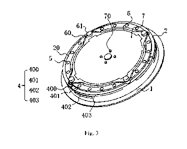
Fig. 3 illustrates a structural schematic diagram of the
multifunctional GNSS antenna of an embodiment of the present disclosure;
Fig. 4 illustrates the front view of Fig. 3;
Fig. 5 illustrates a schematic sectional diagram of the multifunctional
GNSS antenna of an embodiment of the present disclosure; and
Fig. 6 illustrates a structural schematic diagram of the second
dielectric plate of an embodiment of the present disclosure.
The corresponding relationship of the reference signs and the names
of the component in Fig.1 to Fig.6 is that:
1, PCB; 2, first dielectric board; 3, first radiating component; 4,
second radiating component; 5, metallized vias; 6, second dielectric board; 7,
third radiating component; 8, shielding cover; 20, boss; 21, cavity; 22,
positioning groove; 30, first feeding component; 40, second feeding component;
41, grounding short-circuit post; 60, positioning block; 61, stud; 70, third
feeding
4
Date recue/ date received 2022-02-18
CA 03151873 2022-02-18
component; 300, first tuning stub; 400, first metal layer; 401, second metal
layer;
402, third metal layer; 403, fourth metal layer; 700, second tuning stub.
DETAILED DESCRIPTION
The exemplary embodiments will be described in detail here,
examples being shown in the drawings. The same numbers in different drawings
indicate the same or similar elements when the following description refers to
the
drawings, unless otherwise indicated. The implementation manners described in
the following exemplary embodiments do not represent all implementation
manners consistent with the present disclosure. On the contrary, they are
merely
examples of devices and methods consistent with some aspects of the present
disclosure as detailed in the appended claims.
Referring to Fig.1 to Fig.6, the embodiments of the present
disclosure provide a multifunctional GNSS antenna mainly comprising: a PCB 1,
a first dielectric plate 2, and a first radiating component 3 arranged in
sequence,
the PCB 1 is connected with the first radiating component 3 by a first feeding
component 30, a second radiating component 4 and a plurality of metalized vias
5
are arranged on the first dielectric plate 2, the second radiating component 4
is
connected with the PCB 1, the plurality of metalized vias 5 are arranged
around
the first radiating component 3; and the second radiating component 4 is
arranged
on an outer side of the plurality of metalized vias 5.
During the operation, as shown in Fig.2, the current generated by
second radiating component 4 will be coupled to the first radiating component
3,
thereby coupling and interfering with the signal of the first radiating
component
3, affecting the performance of the first radiating component 3. In the
embodiment, the current on the second radiating component 4 is intervened by
means of the plurality of metalized vias 5, so that the current generated on
the
second radiating component 4 is coupled to the metalized vias 5 and part of
the
current is radiated out, thereby the energy coupled to the first radiating
component 3 is reduced, which improves the isolation and interference of the
antenna. In addition, after the current generated by the first radiating
component
5
Date recue/ date received 2022-02-18
CA 03151873 2022-02-18
3 is coupled to the metalized vias 5, the radiating aperture of the first
radiating
component 3 increases, which reduces the frequency of the first radiating
component 3, therefore, the size of the first radiating component 3 decreases
while remaining the same resonant frequency, which is beneficial to realize
the
miniaturization of the antenna.
In an alternative embodiment, the PCB 1, the first dielectric board 2,
the first radiating component 3, and the first feeding component 30 constitute
a
first antenna unit selectively to realize the function of navigation and
positioning.
The PCB 1, the first dielectric board 2, the second radiating component 4, and
the
second feeding component 40 constitute a second antenna unit selectively to
realize the function of communication, such as 4G communication, Bluetooth
communication, etc. Therefore, based on the technical solution of the
embodiments of the present disclosure, the integration of the navigation and
positioning antenna and the communication antenna can be realized, so that the
navigation and positioning, communication and other functions can be realized
by one entire antenna, while the interference and coupling of the
communication
antenna to the navigation and positioning antenna can be reduced and the
effect
of miniaturization of the antenna can be realized.
In an embodiment of the present application, the metalized vias 5 can
be selected to be arranged uniformly along the periphery of the first
radiating
component 3. The plurality of metallized vias 5 can be selected to surround
the
entire periphery of the first radiating component 3 to form a ring structure,
that is
to say to form a protective ring for the first radiating component 3 located
in the
ring structure, so as to avoid the signal interference and coupling of the
antenna
device outside the protection ring to the first radiating component 3.
Further, a boss 20 on which the metallized vias 5 are provided is
arranged on the first dielectric plate 2and around the first radiating
component 3.
In the embodiment, the coupling effect of the metalized vias 5 to the first
radiating component 3 and the second radiating component 4 is further improved
by the boss 20, thereby improving the isolation extent between the first
antenna
unit and the second antenna unit.
As shown from Fig.3 to Fig.6, the multifunctional GNSS antenna
6
Date recue/ date received 2022-02-18
CA 03151873 2022-02-18
further comprises a second dielectric plate 6 arranged on the first radiating
component 3 and a third radiating component 7 arranged on the second
dielectric
plate 6 and connected with the PCB 1 by means of the third feeding component
70. In the embodiment, the second dielectric plate 6, the third radiating
component 7, and the third feeding component 70 can be selected as part of the
first antenna unit, wherein the first radiating component 3 and the third
radiating
component 7 generate different frequency bands respectively. In a specific
embodiment, the first radiating component 3 is configured to generate a
resonant
frequency corresponding to the GNSS L2 frequency band, the third radiating
component 7 is configured to generate a resonant frequency corresponding to
the
GNSS Li frequency band, and the first antenna unit covers the frequency range
of the GNSS Li and GNSS L2, thereby realizing the function of GNSS
navigation and positioning.
The boss 20 extends above the first dielectric plate 2, and a cavity 21
for the installation of the second dielectric plate 6 in the embodiment is
formed in
the inner ring of the boss 20. Optionally, the boss 20 comprises multiple
sections,
a positioning groove 22 is arranged between two adjacent sections of the boss
20.
A positioning block 60 corresponding to the positioning groove 22 is arranged
on
the second dielectric plate 6, the positioning block 60 is embedded in the
positioning slot 22 when installing the second dielectric board 6. In this
embodiment, the second dielectric board 6 can be quickly positioned by means
of
the cooperating structure of the positioning groove 22 and the positioning
block
60, which facilitates the installation of the second dielectric board 6.
In an alternative embodiment, the second dielectric plate 6 is
fastened to the first dielectric plate 2 by a stud 61, so as to avoid the
loosening of
the second dielectric plate 6. In a specific embodiment, the positioning block
60
can be selectively fastened to the positioning groove 22 by the stud 61,
wherein
the positioning groove 22 may be provided with the above metalized vias 5
cooperated with the stud 61. The metalized vias 5 has the function of
fastening of
the first dielectric plate 2 and the second dielectric plate 6, and the stud
61 can be
selected as an insulating plastic stud or a conductive metal stud.
In an embodiment of the present application, the PCB 1 is provided
7
Date recue/ date received 2022-02-18
CA 03151873 2022-02-18
with a first circuit network and a second circuit network, wherein the first
circuit
network comprises a feeding network, a first filter circuit, and a low-noise
amplifier circuit connected sequentially, the feeding network being connected
to
the first feeding component 30 and the third feeding component 70
respectively.
In this embodiment, after the signal is received by the GNSS antenna, the
signal
transfers through the feeding networks firstly, then the first filter circuit
filters
out the communication signals in the signal, such as 4G communication signals,
Bluetooth communication signals, etc. via the first filter circuit, finally,
the
filtered signal is amplified by a low-noise amplifier circuit. Due to the
function
of the first filter circuit, the communication signal is filtered out,
therefore, the
signal interference of the communication antenna can be avoided and the
accuracy of navigation and positioning can be ensured. The second circuit
network comprises a second filter circuit connected with the second feeding
component 40. The navigation positioning signal and irrelevant communication
signals in the signal are filtered out after the signal transfers through the
second
filter circuit, for example, the second radiating component 4 is configured to
implement 4G communication, while the second filter circuit being further
configured to filter out other communication signals apart from the 4G
communication signals so as to avoid the interference of other signals.
The first circuit network and the second circuit network can be
selectively arranged on the side of the PCB board 1 facing away from the first
dielectric board 2. To this end, in an alternative embodiment, a shielding
cover 8
is arranged on the side of the PCB board 1 facing away from the first
dielectric
board 2, the first circuit network and the second circuit network are covered
in
the shielding cover 8 to prevent interference from external signals.
The first feeding component 30, the second feeding component 40,
and the third feeding component 70 can be selected as coaxial probes, taking
the
first feeding component 30 as an example, the coaxial probes pass through the
first dielectric plate 2 and the first radiating component 3 in sequence, with
one
end being connected to the first radiating component 3 and the other end being
connected to the PCB 1. In an alternative embodiment, the first feeding
component 30 and the third feeding component 70 can be selected as a plurality
of, preferably four coaxial probes, and the second feeding component 40 can be
8
Date recue/ date received 2022-02-18
CA 03151873 2022-02-18
selected as one coaxial probe.
In an embodiment of the present application, the second radiating
component 4 is further provided with a grounding short-circuit post 41.
Specifically, the grounding short-circuit post 41 penetrates the second
radiating
component 4, the first dielectric plate 2 and the PCB 1. One end of the
grounding
short-circuit post 41 is connected to the second radiating component 4, and
the
other end is connected to ground, for example, the grounded end of the
grounding
short-circuit post 41 can be selected to connect to a ground plate.
It should be noted that, in an embodiment of the present application,
the ground to which the grounding short-circuit post 41 is connected is the
same
ground as the bottom surface of the first dielectric plate 2. It can also be
understood that the ground to which the grounding short-circuit post 41 is
connected is different from the bottom surface of the first dielectric plate
6.
Therefore, after arranging the second dielectric plate 6 and the third
radiating
component 7, the signal generated by the second radiating component 4 has
little
effect on the signal generated by the third radiating component 7.
In an alternative embodiment, the second radiating component 4
comprises a plurality of metal layers connected with each other, the plurality
of
metal layers comprises at least one metal layer arranged on the surface of the
first
dielectric plate 2 and at least one metal layer arranged on the side surface
of the
first dielectric plate 2. In this embodiment, the second radiating component 4
is
an inverted-F antenna type, and the plurality of metal layers have different
sizes,
therefore, the plurality of metal layers have different resonant frequencies
to
match the signals of different frequency bands. In a specific embodiment, the
second radiating component 4 comprises a first metal layer 400, a second metal
layer 401, a third metal layer 402, and a fourth metal layer 403, wherein the
first
metal layer 400 is arranged on the edge of the upper surface of the first
dielectric
plate 2, the second metal layer 401, the third metal layer 402, and the fourth
metal layer 403 are arranged on the side surface of the first dielectric plate
2. The
second metal layer 401 and the third metal layer 402 are connected to the
first
metal layer 400 respectively, and the third metal layer 402 is further
connected to
the fourth metal layer 403. In this embodiment, the second radiating component
4
9
Date recue/ date received 2022-02-18
CA 03151873 2022-02-18
realizes horizontal omnidirectional radiating.
In an alternative embodiment, the GNSS antenna comprises a
plurality of second radiating components 4 arranged in circumferential
direction
along the perimeter of the first dielectric plate 2. Wherein the plurality of
second
radiating components 4 can be selected to implement different functions, for
example, the plurality of second radiating components 4 can be selected to
comprise: a second radiating component 4 configured to realize 4G
communication function and a second radiating component 4 configured to
realize Bluetooth communication function. In a specific embodiment, there are
three of the second radiating components 4, wherein one of the second
radiating
components 4 is configured to realize Bluetooth communication, and the other
two are configured to realize 4G communication. In this embodiment, the second
radiating component 4 configured to realize Bluetooth communication form a
Bluetooth antenna together with the PCB 1, the first dielectric board 2 and
the
corresponding second feeding component 5, the second radiating component 4
for realizing 4G communication form a 4G communication antenna together with
the PCB board 1, the first dielectric board 2, and the corresponding second
feeding component, wherein the 4G communication antenna adopts two radiating
components for high-speed data transmission, in general, one radiating
component can also be adopted by the 4G communication antenna.
In an embodiment of the present application, the first radiating
component 3 can be selected as a metal layer attached to the upper surface of
the
first dielectric plate 2, and the third radiating component 7 can be selected
as a
metal layer attached to the upper surface of the second dielectric plate 6.
The edge of the first radiating component 3 is provided with a first
tuning stub 300 extending outward, configured to fine-tune the resonant
frequency of the first radiating component 3; the edge of the third radiating
component 7 is provided with a second tuning stub 700 extending outward,
configured to fine-tune the resonant frequency of the third radiating
component
4.
In summary, the multifunctional GNSS antenna of the embodiments
of the present disclosure has the functions of GNSS navigation and
positioning,
Date recue/ date received 2022-02-18
CA 03151873 2022-02-18
4G communication and Bluetooth communication at the same time, with the
multiple antenna functions integrating on one antenna, which significantly
saves
the installation space compared to multiple antennas designed separately.
Based
on the integration of multiple antennas, in the embodiments of the present
disclosure, each antenna has good isolation and anti-interference ability
respect
to another, therefore, the performance of the multifunctional GNSS antenna can
be ensured, especially the interference and coupling of the communication
antenna to it can be reduced when the first antenna unit is used as a
navigation
and positioning antenna to ensure the positioning accuracy and avoid the
phenomenon of satellite lock-out; the metalized vias further couple with the
first
radiating component, thereby increasing the radiating aperture of the first
radiating component, so that the resonant frequency of the first radiating
component is reduced, accordingly, in order to achieve the preset resonant
frequency, the required size of the first radiating component is
correspondingly
reduced, further causing the size of the entire antenna to reduce
correspondingly,
which is beneficial to the miniaturized design of the antenna.
In the description of this disclosure, it should be noted that the
orientation or positional relationship indicated by the terms "upper",
"lower", etc.
is based on the orientation or positional relationship shown in the
accompanying
.. drawings, and is only used for the convenience of describing the disclosure
and
simplifying the description, but not to indicate or imply that the device or
element referred to must have a particular orientation, be constructed and
operate
in a particular orientation, and therefore should not be construed as limiting
the
disclosure. Furthermore, the terms "first" and "second" are used for
descriptive
purposes only and should not be construed to indicate or imply relative
importance.
In the description of this disclosure, it should be noted that, unless
otherwise expressly specified and limited, the terms "installation",
"communication" and "connection" should be understood in a broad sense, for
example, it may be a fixed connection or a detachable connection, or integral
connection; may be mechanical connection or electrical connection; may be
direct communication, or indirect communication by means of an intermediate
medium, or internal communication between two elements. For those of ordinary
11
Date recue/ date received 2022-02-18
CA 03151873 2022-02-18
skilled in the art, the specific meanings of the above terms in this
disclosure can
be understood in specific situations. Furthermore, in the description of this
disclosure, unless otherwise specified, "plurality" means two or more.
The above are only preferred embodiments of the present disclosure,
and are not intended to limit the present disclosure. Any modifications,
equivalent replacements, improvements, etc. made within the spirit and
principles
of the present disclosure shall be included in the protection range of the
present
disclosure.
12
Date recue/ date received 2022-02-18