Note: Descriptions are shown in the official language in which they were submitted.
CA 03153651 2022-03-07
Description
Title of the Invention: SEMICONDUCTOR MACH-ZEHNDER OPTICAL
MODULATOR AND IQ MODULATOR
Technical Field
[0001] The present invention relates to a semiconductor Mach-
Zehnder modulator that modulates an optical signal with an
electric signal, and an IQ modulator in which semiconductor
Mach-Zehnder modulators are used.
Background Art
[0002] In order to meet an increasing demand for communication
traffic, a high-speed optical modulator adaptable to a high-
level optical modulation method is demanded. In particular,
high-order optical modulators through use of the digital
coherent technology play a great role in achieving transceivers
having a large capacity exceeding 100 Gbps. In these high-order
optical modulators, MZ (Mach-Zehnder) interference optical
modulators capable of zero chirp driving are included in
parallel and in multiple stages so as to add independent signals
to the amplitude and phase of light, respectively.
[0003] Recent challenges are size reduction of an optical
transmitter module and reduction of a driving voltage, and
research and development of a compact semiconductor MZ modulator
that enables reduction of the driving voltage is being advanced
enthusiastically. Furthermore, in the research and development
of the semiconductor MZ modulator, the movement toward
adaptation to a higher baud rate such as 64 GBaud or 100 GBaud
is being accelerated, and there is a need for the modulator to
adapt to a wider band.
1
=
CA 03153651 2022-03-07
[0004] In the meanwhile, research and development of a HB-CDM
(High Bandwidth Coherent Driver Modulator) intended not only to
improve characteristics with a modulator alone, but also to
improve radio frequency characteristics and achieve size
reduction by integrating a driver and a modulator into a single
package and offering a coordinated design of the driver and the
modulator is being accelerated (see Non-Patent Literature 1).
Since the differentially-driven driver and the modulator are
integrated in the configuration of HB-CDM, it is desirable that
the modulator itself have a differentially-driven configuration.
[0005] In a wideband semiconductor MZ modulator, a traveling
wave electrode is commonly used. In order to improve the
modulation band in the traveling wave electrode, (I) light speed
matching between microwaves propagating through the electrode
and light propagating through a Waveguide, and (II) reduction of
a propagation loss in the electrode are very important. In
order to meet (I) and (II), a capacitively loaded structure is
used in the semiconductor MZ modulator (see Non-Patent
Literature 2 and Non-Patent Literature 3).
[0006] The semiconductor MZ modulator having the capacitively
loaded structure is designed such that a main line for
transmitting a modulation signal and electrodes for separating
the modulation signal from the main line for application to
waveguides are formed to perform phase modulation. By optimally
designing the number of and interval between electrodes branched
from this main line as well as the length of contact of the
electrodes with the waveguides, the amount of capacity to be
added to the main line can be designed freely, and the impedance
of the main line and the speed of microwaves can be designed to
have arbitrary values. In addition, by designing an optimum
2
CA 03153651 2022-03-07
amount of capacity to be added to the main line, speed matching
between optical waves and microwaves can be improved, and
impedance matching to 50 Q can be achieved, as a result of which
adaptation to a wider band can be achieved.
[0007] In addition, the semiconductor MZ modulator having the
capacitively loaded structure is configured such that a voltage
is applied between an underlying n-type semiconductor layer and
a surface electrode, and because of their voltage difference, a
reverse bias is applied to a semiconductor MQW (Multi Quantum
Well) layer, and a modulation operation is performed. The n-
type semiconductor layer is significantly lower in resistance
value than a p-type semiconductor layer, but is higher in
resistance value than metal. Since in the capacitively loaded
structure, the voltage needs to be applied through the n-type
semiconductor layer, a voltage drop is caused by the resistance
of the n-type semiconductor layer in a case in which a current
flows into the n-type semiconductor layer. When a voltage drop
occurs, an absolute amount of a necessary voltage to be applied
to the n-type semiconductor layer for driving increases, which
increases a bias voltage during operation, resulting in a
problem of poor efficiency.
[0008] A specific description will be provided using Fig. 10A
and Fig. 10B. Fig. 10A is a plan view of a semiconductor MZ
optical modulator, and Fig. 10B is a cross-sectional view taken
along the line c-c' in Fig. 10A.
In Fig. 10A and Fig. 10B, an input waveguide of the
semiconductor MZ optical modulator is denoted by 101, an output
waveguide is denoted by 102, an optical branching filter that
separates optical waves propagating through the input waveguide
101 into two waveguides 104, 105 is denoted by 103, an optical
3
=
=
CA 03153651 2022-03-07
multiplexer that multiplexes optical waves propagating through
the two waveguides 104, 105 into the output waveguide 102 is
denoted by 106, coplanar strip lines are denoted by 109, 110,
electrodes for applying a voltage to the waveguides 104, 105 are
denoted by 111, 112, and an electrode pad connected to the
underlying n-type semiconductor layer is denoted by 118.
[0009]
In Fig. 10B, an n-InP layer (n-type semiconductor layer)
is denoted by 113, a lower cladding layer made of InP is denoted
by 114, a semiconductor core layer through which optical waves
propagate is denoted by 115, an upper cladding layer made of InP
is denoted by 116, and an SI-InP substrate is denoted by 117.
[0010] The input waveguide 101, the output waveguide 102, the
optical branching filter 103, the waveguides 104, 105, and the
optical multiplexer 106 constitute a MZ interferometer. In the
MZ interferometer, by applying a voltage to the waveguides 104,
105, the refractive index is changed in the semiconductor core
layer 115 by virtue of an electro-optic effect. As a result,
the phase of light is changed. At this time, by providing a
voltage difference between the waveguides 104, 105, an optical
interference state in the optical multiplexer 106 is changed, so
that light can be modulated (that is, output light of the output
waveguide 102 is turned on and off).
[0011] An SG configuration is presented in which, in a case in
which one of the two coplanar strip lines 109, 110 is connected
to an input electric signal (S), the other is connected to a
reference potential or a ground (G).
[0012] Microwaves propagating through the coplanar strip lines
109, 110 are applied to the waveguides 104, 105 by the
electrodes 111, 112. The electrodes 111, 112 and the coplanar
strip lines 109, 110 form a traveling wave electrode as a whole.
4
=
CA 03153651 2022-03-07
That is, an electrode structure intended to increase the
modulation band by matching the speed of optical waves
propagating through the waveguides 104, 105 and the speed of
microwaves propagating through the above-described traveling
wave electrode as close as possible to achieve phase matching
between the optical waves and the microwaves is presented. If
there is no loss in microwaves, and speed matching conditions
between the optical waves and the microwaves are satisfied
completely, the modulation band will be infinite. However,
reflection of microwaves due to a loss in microwaves or
impedance mismatching and a phase shift between the optical
waves and the microwaves actually occur, and thus the modulation
band is restricted for these reasons.
[0013] Since the upper cladding layer 116, the semiconductor
core layer 115, and the lower cladding layer 114 are present
under the electrodes 111, 112 as described earlier, certain
element capacity is present. That is, in Fig. 10A, the
electrodes 111, 112 add capacity to the coplanar strip lines
109, 110. In other words, by optimally designing the number of
and interval between the electrodes 111, 112 as well as the
length of contact of the electrodes 111, 112 with the waveguides
104, 105, the amount of capacity to be added to the coplanar
strip lines 109, 110 can be freely designed, and the impedance
of the coplanar strip lines 109, 110 and the speed of microwaves
can be designed to have arbitrary values.
[0014] In addition, two electrode pads 118 connected to the n-
InP layer 113 (n-type semiconductor layer) for driving the
modulator are placed at portions away from the coplanar strip
lines 109, 110 and the electrodes 111, 112. These two electrode
pads 118 are arranged at the same position in an extended
CA 03153651 2022-03-07
direction of the waveguides 101, 102, 104, and 105. As
described above, a voltage is applied to the n-type
semiconductor layer through the electrode pads 118 in the
semiconductor MZ modulator having the capacitively loaded
structure, however, a voltage drop is caused by the resistance
of the n-type semiconductor layer, which raises a problem of
poor power efficiency.
Citation List
Non-Patent Literature
[0015] Non-Patent Literature 1: J. Ozaki, et al., "Ultra-low
Power Dissipation (< 2.4 W) Coherent InP Modulator Module with
CMOS Driver IC", Mo3C.2, ECOC, 2018
Non-Patent Literature 2: H. N. Klein et al., "1.55 m
Mach-Zehnder Modulators on InP for optical 40/80 Gbit/s
transmission networks", 0FC2006, pp.171-173, 2006
Non-Patent Literature 3: D. Hoffman et al., "45 GHz
bandwidth travelling wave electrode Mach-Zehnder modulator with
integrated spot size converter", IPRM 2004
Summary of the Invention
Technical Problem
[0016] An object of the present invention, which has been made
to solve the above-described problems, is to prevent a voltage
drop that would occur in a case in which a bias voltage for
operation is applied to an underlying conductive layer in a
semiconductor Mach-Zehnder optical modulator having the
capacitively loaded structure.
6
CA 03153651 2022-03-07
Means for Solving the Problem
[0017] A semiconductor Mach-Zehnder optical modulator of the
present invention includes: an optical waveguide formed on a
semi-insulating semiconductor substrate; an input-side lead-out
line formed on a dielectric layer of at least one layer on the
substrate, a modulation signal being input to one end of the
input-side lead-out line; a phase modulation electrode line
formed on the dielectric layer along the optical waveguide, and
having .one end connected to the other end of the input-side
lead-out line; an electrode that applies the modulation signal
propagating through the phase modulation electrode line to the
optical waveguide; a conductive layer formed between the
substrate and the optical waveguide; a plurality of first wiring
layers formed intermittently in an extended direction of the
optical waveguide so as to cross the optical waveguide, and
connected to the conductive layer; and a second wiring layer
formed to connect an electrode pad for applying a voltage to the
conductive layer and the plurality of first wiring layers.
[0018] In addition, in a configuration example of the
semiconductor Mach-Zehnder optical modulator of the present
invention, the first wiring layers are made of any of an n-type
semiconductor layer, metal, and a structure in which metal is
formed on an n-type semiconductor layer, and the second wiring
layer is made of metal.
In addition, in a configuration example of the
semiconductor Mach-Zehnder optical modulator of the present
invention, the first and second wiring layers are formed closer
to the substrate than to the input-side lead-out line and the
phase modulation electrode line, respectively.
7
CA 03153651 2022-03-07
In addition, in a configuration example of the
semiconductor Mach-Zehnder optical modulator of the present
invention, a plurality of the electrodes are provided
periodically in the extended direction of the optical waveguide,
and a first wiring layer of the plurality of first wiring layers
that is formed in a region of the phase modulation electrode
line is arranged at a central position between two electrodes
adjacent to each other in the extended direction of the optical
waveguide.
[0019] In addition, a configuration example of the
semiconductor Mach-Zehnder optical modulator of the present
invention further includes an output-side lead-out line formed
on the dielectric layer, and having one end connected to the
other end of the phase modulation electrode line, in which the
optical waveguide includes two first and second arm waveguides,
the input-side lead-out line includes a first input-side lead-
out line, a modulation signal being input to one end of the
first input-side lead-out line, and a second input-side lead-out
line formed on the dielectric layer adjacent to the first input-
side lead-out line, a signal complementary to the modulation
signal being input to one end of the second input-side lead-out
line, the phase modulation electrode line includes two first and
second phase modulation electrode lines formed on the dielectric
layer along the first and second arm waveguides, and having one
ends respectively connected to the other ends of the first and
second input-side lead-out lines, the output-side lead-out line
includes two first and second output-side lead-out lines having
one ends respectively connected to the other ends of the first
and second phase modulation electrode lines, and the electrode
includes two first and second electrodes that respectively apply
8
CA 03153651 2022-03-07
modulation signals propagating through the first and second
phase modulation electrode lines to the first and second arm
waveguides. The semiconductor Mach-Zehnder optical modulator
further includes: a first ground line formed in the extended
direction of the optical waveguide on the dielectric layer
outside the first input-side lead-out line, the first phase
modulation electrode line, and the first output-side lead-out
line; and a second ground line formed in the extended direction
of the optical waveguide on the dielectric layer outside the
second input-side lead-out line, the second phase modulation
electrode line, and the second output-side lead-out line.
[0020] In addition, an IQ modulator of the present invention
includes: two semiconductor Mach-Zehnder optical modulators; an
input Waveguide formed on the substrate; and a branching filter
formed on the substrate to separate light propagating through
the input waveguide into two systems for input to the two
semiconductor Mach-Zehnder optical modulators, in which, of the
two semiconductor Mach-Zehnder optical modulators, a first
semiconductor Mach-Zehnder optical modulator that receives an I
modulation signal as an input and a second semiconductor Mach-
Zehnder optical modulator that receives a Q modulation signal as
an input are arranged such that their optical waveguides are
located in parallel to each other, the second ground line of the
first semiconductor Mach-Zehnder optical modulator and the first
ground line of the second semiconductor Mach-Zehnder optical
modulator adjacent to the second ground line are formed
integrally as a ground line common to the two semiconductor
Mach-Zehnder optical modulators, and in the second wiring layer,
a portion arranged in the extended direction of the optical
9
CA 03153651 2022-03-07
waveguide is arranged under a centerline of the common ground
line.
In addition, a configuration example of the IQ modulator
of the-present invention is connected from a single electrode
pad to the first wiring layers of each of the first and second
semiconductor Mach-Zehnder optical modulators through the second
wiring layer.
In addition, in a configuration example of the IQ
modulator of the present invention, the plurality of wiring
layers are each formed from a position under the first ground
line of the first semiconductor Mach-Zehnder optical modulator
to a position under the second ground line of the second
semiconductor Mach-Zehnder optical modulator, and a distance
from the second wiring layer to an end close to the first
semiconductor Mach-Zehnder optical modulator and a distance from
the second wiring layer to an end close to the second
semiconductor Mach-Zehnder optical modulator are equal.
Effects of the Invention
[0021] According to the present invention, by providing the
plurality of first wiring layers formed intermittently in the
extended direction of the optical waveguide, and connected to
the conductive layer, and the second wiring layer formed to
connect the electrode pad and the plurality of first wiring
layers, a voltage drop that would be caused by the resistance of
the conductive layer such as an n-type semiconductor layer when
driving a capacitively loaded semiconductor Mach-Zehnder optical
modulator can be prevented without deteriorating RF
characteristics. As a result, the present invention can provide
an excellent differential capacitively loaded semiconductor
CA 03153651 2022-03-07
Mach-Zehnder optical modulator driven at a low bias voltage and
capable of a high baud rate operation.
Brief Description of Drawings
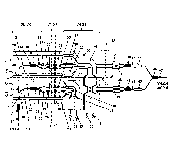
[0022] [Fig. 1] Fig. 1 is a plan view illustrating a
configuration of an IQ modulator according to a first embodiment
of the present invention.
[Fig. 2] Fig. 2 is a cross-sectional view of a phase
modulation portion of the IQ modulator according to the first
embodiment of the present invention.
[Fig. 3] Fig. 3 is a cross-sectional view of the phase
modulation portion of the IQ modulator according to the first
embodiment of the present invention.
[Fig. 4] Fig. 4 is a cross-sectional view of a portion
of a ground line of the IQ modulator according to the first
embodiment of the present invention.
[Fig. 5] Fig. 5 is another cross-sectional view of the
portion of the ground line of the IQ modulator according to the
first embodiment of the present invention.
[Fig. 6] Fig. 6 is a cross-sectional view of a phase
modulation portion of an IQ modulator according to a second
embodiment of the present invention.
[Fig. 7] Fig. 7 is a cross-sectional view of a portion
of a ground line of the IQ modulator according to the second
embodiment of the present invention.
[Fig. 8] Fig. 8 is a cross-sectional view of a phase
modulation portion of an IQ modulator according to a third
embodiment of the present invention.
11
CA 03153651 2022-03-07
[Fig. 9] Fig. 9 is a cross-sectional view of a portion
of a ground line of the IQ modulator according to the third
embodiment of the present invention.
[Fig. 10A] Fig. 10A is a plan view illustrating a
configuration of a conventional semiconductor MZ modulator.
[Fig. 10B] Fig. 10B is a cross-sectional view
illustrating the configuration of the conventional semiconductor
HZ modulator.
Description of Embodiments
[0023] [Principles of invention]
In the present invention, a plurality of wiring layers
for applying a voltage to an underlying n-type semiconductor
layer (conductive layer) are prepared in order to prevent an
increase in bias voltage necessary for operating a capacitively
loaded semiconductor HZ modulator. Furthermore, by providing
connection wiring having a predetermined structure, an influence
upon RF (Radio Frequency) characteristics due to the presence of
the wiring layers is minimized.
[0024] [First embodiment]
Hereinafter, embodiments of the present invention will
be described with reference to the drawings. Fig. 1 is a plan
view illustrating a configuration of an IQ modulator according
to a first embodiment of the present invention. Fig. 1 depicts
a phase modulation portion of the IQ modulator composed of two
semiconductor HZ modulators.
[0025] The IQ modulator includes an input waveguide 10, a 1x2
MMI coupler 11, waveguides 12, 13, a 1x2 MMI coupler 14, a 1x2
MMI coupler 15, waveguides 16, 17 (first and second arm
waveguides), waveguides 18, 19 (first and second arm
12
CA 03153651 2022-03-07
waveguides), input-side lead-out lines 20, 21 (first and second
input-side lead-out lines), input-side lead-out lines 22, 23
(first and second input-side lead-out lines), phase modulation
electrode lines 24, 25 (first and second phase modulation
electrode lines), phase modulation electrode lines 26, 27 (first
and second phase modulation electrode lines), output-side lead-
out lines 28, 29 (first and second output-side lead-out lines),
output-side lead-out lines 30, 31 (first and second output-side
lead-out lines), electrodes 32, 33 (first and second
electrodes), and electrodes 34, 35 (first and second
electrodes). The aforementioned 1x2 MMI coupler 11 separates
light propagating through the input waveguide 10 into two
systems. The aforementioned waveguides 12, 13 guide the two
rays of light separated by the 1x2 MMI coupler 11. The
aforementioned 1x2 MMI coupler 14 separates light propagating
through the waveguide 12 into two systems. The aforementioned
1x2 MMI coupler 15 separates light propagating through the
waveguide 13 into two systems. The aforementioned waveguides
16, 17 guide the two rays of light separated by the 1x2 MMI
coupler 14. The aforementioned waveguides 18, 19 guide the two
rays of light separated by the 1x2 MMI coupler 15. The
aforementioned input-side lead-out lines 20, 21 are made of a
conductor for applying an I modulation signal to the waveguides
16, 17. The aforementioned input-side lead-out lines 22, 23 are
made of a conductor for applying a Q modulation signal to the
waveguides 18, 19. The aforementioned phase modulation
electrode lines 24, 25 are made of a conductor connected to the
input-side lead-out lines 20, 21. The aforementioned phase
modulation electrode lines 26, 27 are made of a conductor
connected to the input-side lead-out lines 22, 23. The
13
CA 03153651 2022-03-07
aforementioned output-side lead-out lines 28, 29 are made of a
conductor connected to the phase modulation electrode lines 24,
25. The aforementioned output-side lead-out lines 30, 31 are
made of a conductor connected to the phase modulation electrode
lines 26, 27. The aforementioned electrodes 32, 33 are made of
a conductor for applying an I modulation signal supplied from
the phase modulation electrode lines 24, 25 to the waveguides
16, 17. The aforementioned electrodes 34, 35 are made of a
conductor for applying a Q modulation signal supplied from the
phase modulation electrode lines 26, 27 to the waveguides 18,
19.
[0026] Furthermore, the dual-polarization IQ modulator includes
phase adjustment electrodes 36 to 39, a 2x1 MMI coupler 40, a 2x1
MMI coupler 41, a waveguide 42, a waveguide 43, phase adjustment
electrodes 44, 45, a 2x1 MMI coupler 46, an output waveguide 47,
a ground line 48, a ground line 49, a ground line 50,
termination resistors 51 to 54, and an electrode pad 55. The
aforementioned phase adjustment electrodes 36 to 39 are made of
a conductor for adjusting the phase of modulated signal light
propagating through the waveguides 16 to 19. The aforementioned
2x1 MMI coupler 40 multiplexes signal light in the two systems
propagating through the waveguides 16, 17. The aforementioned
2x1 MMI coupler 41 multiplexes signal light in the two systems
propagating through the waveguides 18, 19. The aforementioned
waveguide 42 guides output light of the 2x1 MMI coupler 40. The
aforementioned waveguide 43 guides output light of the 2x1 MMI
coupler 41. The aforementioned phase adjustment electrodes 44,
45 are made of a conductor for adjusting the phase of signal
light propagating through the waveguides 42, 43. The
14
CA 03153651 2022-03-07
aforementioned 2x1 MMI coupler 46 multiplexes signal light in the
two systems propagating through the waveguides 42, 43. The
aforementioned ground line 48 is made of a conductor provided
outside the 2x1 MMI coupler 46, the output waveguide 47, the
input-side lead-out line 20, the phase modulation electrode line
24, and the output-side lead-out line 28. The aforementioned
ground line 49 is made of a conductor provided between the
input-side lead-out line 21, the phase modulation electrode line
25, and the output-side lead-out line 29, and the input-side
lead-out line 22, the phase modulation electrode line 26, and
the output-side lead-out line 30. The aforementioned ground
line 50 is made of a conductor provided outside the input-side
lead-out line 23, the phase modulation electrode line 27, and
the output-side lead-out line 31. The aforementioned
termination resistors 51 to 54 are connected to ends of the
output-side lead-out lines 28 to 31. The aforementioned
electrode pad 55 applies a voltage to the underlying n-type
semiconductor layer.
[0027] A radio frequency line of the IQ modulator of the
present embodiment is formed from three portions: the portion of
the input-side lead-out lines 20 to 23; the portion of the phase
modulation electrode lines 24 to 27; and the portion of the
output-side lead-out lines 28 to 31, and in all the portions
presents a differential line structure (GSSG configuration) in
which impedance matching is achieved. If impedance matching is
not achieved, signal reflection would occur at connections in
the radio frequency line, causing the radio frequency
characteristics to deteriorate.
[0028] In the present embodiment, the radio frequency line has
the differential line configuration in all the portions, so that
CA 03153651 2022-03-07
the modulator can be driven by a differential input signal
(differential driver) having a high energy efficiency. In
addition, in the present embodiment, the radio frequency line
having the differential line configuration can achieve smooth
radio frequency connection even with an open collector or open
drain differential driver recently used from the perspective of
reducing power consumption, and both low power consumption and
broadband performance can be achieved.
[0029] Next, a radio frequency line pattern of the present
embodiment will be described in more detail. As described
above, the radio frequency line pattern of the present
embodiment adopts, as a basic structure, a GSSG (ground signal
signal ground) differential coplanar line composed of two signal
lines and two ground lines formed on a dielectric layer made of
a low-dielectric material.
[0030] However, in the present embodiment, the semiconductor MZ
modulator that receives an I modulation signal as an input and
the semiconductor MZ modulator that receives a Q modulation
signal as an input are arranged on a substrate in parallel such
that their waveguides are located in parallel to each other.
[0031] In the present embodiment, the radio frequency line
pattern of the semiconductor MZ modulator on the I modulation
signal side and the radio frequency line pattern of the
semiconductor MZ modulator on the Q modulation signal side share
the ground line 49 at the center. That is, a ground line of the
semiconductor MZ modulator on the I modulation signal side and a
ground line of the semiconductor MZ modulator on the Q
modulation signal side adjacent thereto are formed integrally as
a ground line common to these two semiconductor MZ optical
modulators.
16
CA 03153651 2022-03-07
[0032] An I modulation signal is input to the input-side lead-
out line 20 from a differential driver (not shown) formed on a
SI-InP.substrate which will be described later, and an I
modulation signal (bar I) complementary thereto is input to the
input-side lead-out line 21 from the differential driver.
Similarly, a Q modulation signal is input to the input-side
lead-out line 22 from the differential driver, and a Q
modulation signal (bar Q) complementary thereto is input to the
input-side lead-out line 23 from the differential driver.
[0033] The phase modulation electrode lines 24 to 27 are
provided in parallel to the waveguides 16 to 19 constituting the
semiconductor MZ modulator. The phase modulation electrode
lines 24 to 27 and the electrodes 32 to 35 connected thereto
form a differential capacitively loaded structure (GSSG
configuration) excellent in impedance matching and speed
matching between microwaves and optical waves.
[0034] That is, it is configured such that the ground line 48,
the phase modulation electrode line 24 to which an I modulation
signal is input, the electrode 32 to which the I modulation
signal is supplied from the phase modulation electrode line 24,
the electrode 33 to which a signal (bar I) complementary to the
I modulation signal is input, the phase modulation electrode
line 25 that supplies the signal to the electrode 33, the ground
line 49, the phase modulation electrode line 26 to which a Q
modulation signal is input, the electrode 34 to which the Q
modulation signal is supplied from the phase modulation
electrode line 26, the electrode 35 to which a signal (bar Q)
complementary to the Q modulation signal is input, the phase
modulation electrode line 27 that supplies the signal to the
electrode 35, and the ground line 50 are aligned.
17
CA 03153651 2022-03-07
[0035] By optimally designing the number of, interval between,
and length of the electrodes 32 to 35 of the capacitively loaded
portion branched from the phase modulation electrode lines 24 to
27 which are main lines and formed periodically, the amount of
capacity to be added to the phase modulation electrode lines 24
to 27 can be designed freely, so that impedances of the phase
modulation electrode lines 24 to 27 and the speed of microwaves
propagating through the phase modulation electrode lines 24 to
27 can be designed to have arbitrary values.
[0036] The input-side lead-out lines 20 to 23 may have the GSSG
configuration, or may have a GSGSG configuration (a
configuration obtained by further adding a ground line between
the input-side lead-out lines 20 and 21 and a ground line
between the input-side lead-out lines 22 and 23 to the GSSG
configuration). In general, the differential capacitively
loaded structure of the phase modulation portion has the GSSG
configuration in many cases, and the present embodiment also
adopts the GSSG configuration. Thus, the input-side lead-out
lines 20 to 23 and the output-side lead-out lines 28 to 31 are
also radio frequency lines of the GSSG configuration.
[0037] The reason why the input-side lead-out lines 20 to 23
and the output-side lead-out lines 28 to 31 have the GSSG
configuration identical to the phase modulation portion is
because of concerns about losses and deterioration in
characteristics due to a mode change such as a change from the
GSGSG configuration to the GSSG configuration or a change from
the GSSG configuration to the GSGSG configuration. If the phase
modulation portion has the GSGSG configuration, it is desirable
that the input-side lead-out lines 20 to 23 and the output-side
lead-out lines 28 to 31 have the GSGSG configuration.
18
CA 03153651 2022-03-07
[0038] The respective ends of the output-side lead-out lines 28
to 31 are terminated by the radio frequency termination
resistors 51 to 54. Ends of the radio frequency termination
resistors 51 to 54 that are not connected to the output-side
lead-out lines 28 to 31 are grounded or set at an arbitrary
potential.
One ends of the ground lines 48 to 50 (on the left end
in Fig. 1) are connected to the ground of the differential
driver.
[0039] The 1x2 MMI coupler 14, the waveguides 16, 17, the
input-side lead-out lines 20, 21, the phase modulation electrode
lines 24, 25, the output-side lead-out lines 28, 29, the
electrodes 32, 33, and the 2x1 MMI coupler 40 constitute the I-
side semiconductor MZ modulator. This semiconductor MZ
modulator modulates the phase of light propagating through the
waveguides 16, 17 in accordance with the I modulation signal
applied from the electrodes 32, 33 to the waveguides 16, 17.
[0040] Similarly, the 1x2 MMI coupler 15, the waveguides 18,
19, the input-side lead-out lines 22, 23, the phase modulation
electrode lines 26, 27, the output-side lead-out lines 30, 31,
the electrodes 34, 35, and the 2x1 MMI coupler 41 constitute the
Q-side semiconductor MZ modulator. This semiconductor MZ
modulator modulates the phase of light propagating through the
waveguides 18, 19 in accordance with the Q modulation signal
applied from the electrodes 34, 35 to the waveguides 18, 19.
[0041] The 2x1 MMI coupler 40 multiplexes modulated signal
light propagating through the waveguides 16, 17, and the 2x1 MMI
coupler 41 multiplexes modulated signal light propagating
through the waveguides 18, 19. By applying a voltage to the
phase adjustment electrodes 44, 45, the phase can be adjusted
19
CA 03153651 2022-03-07
such that a phase difference between the I-side signal light
output from the 2x1 MMI coupler 40 and the Q-side signal light
output from the 2x1 MMI coupler 41 is 90 degrees.
[0042] The 2x1 MMI coupler 46 multiplexes the I-side signal
light propagating through the waveguide 42 and the Q-side signal
light propagating through the waveguide 43 to obtain an optical
IQ modulation signal. In the present embodiment, the IQ
modulator can thus be achieved.
[0043] Since the semiconductor MZ optical modulator of the
present embodiment has the capacitively loaded structure, a bias
voltage for driving the modulator needs to be applied through
the underlying conductive layer (n-type semiconductor layer),
similarly to those disclosed in Non-Patent Literature 2 and Non-
Patent Literature 3. If the underlying conductive layer through
which the bias voltage is to be applied is a p-type
semiconductor layer, a voltage drop would be increased because
of its high resistivity. The voltage drop in the case in which
the conductive layer is the p-type semiconductor layer is larger
by about one digit than in the case of an n-type semiconductor
layer. Therefore, the conductive layer through which the bias
voltage is to be applied definitely needs to be an n-type
semiconductor layer.
[0044]
Fig. 2 is a cross-sectional view of the phase modulation
portion (the region in which the electrodes 32 to 35 and the
phase modulation electrode lines 24 to 27 are present) of the IQ
modulator of the present embodiment, and is a cross-sectional
view taken along the line a-a' in Fig. 1. The phase modulation
portion has a differential capacitively loaded structure in
which the electrodes 32 to 35 branched from the phase modulation
electrode lines 24 to 27 (main lines) formed on the dielectric
CA 03153651 2022-03-07
layer and having a T-shape as viewed in plan view are formed on
the waveguides 16 to 19, and modulation signals are applied to
the waveguides 16 to 19.
[0045] The waveguides 16 to 19 in the phase modulation portion
are formed from a waveguide structure in which an n-type
semiconductor layer (for example, a quaternary layer such as n-
InP or n-InGaAsP) 60, a lower cladding layer 61 made of
semiconductor, a semiconductor core layer 62, and an upper
cladding layer 63 are laminated sequentially on the SI-InP
substrate 64.
[0046] The input-side lead-out lines 20 to 23, the phase
modulation electrode lines 24 to 27, the output-side lead-out
lines 28 to 31, and the ground lines 48 to 50 are formed on a
dielectric layer 65. In order to reduce losses of the radio
frequency lines, the dielectric layer 65 is desirably formed of
a low-dielectric material such as, for example, Benzocyclobutene
(BOB)
[0047] Either one of the upper cladding layer 63 and the lower
cladding layer 61 may be an n-type semiconductor, and the other
may be a p-type semiconductor. Alternatively, a structure may
be adopted in which both the upper cladding layer 63 and the
lower cladding layer 61 are n-type semiconductors, and a third
p-type cladding layer is inserted between the upper cladding
layer 63 and the semiconductor core layer 62 or between the
lower cladding layer 61 and the semiconductor core layer 62.
[0048] Next, a structure for preventing a voltage to be applied
to the n-type semiconductor layer 60 (conductive layer) from
dropping will be described. Fig. 3 is a cross-sectional view of
the phase modulation portion of the IQ modulator of the present
embodiment, and is a cross-sectional view taken along the line
21
CA 03153651 2022-03-07
b-b' in Fig. 1. Fig. 4 is a cross-sectional view of the portion
of the ground line 49 of the IQ modulator of the present
embodiment, and is a cross-sectional view taken along the line
d-d' in Fig. 1.
[0049] In the present embodiment, an n-type semiconductor layer
60a is formed in each of three regions 70 illustrated in Fig. 1.
When considering the resistivity, a p-type semiconductor is not
preferable for a first wiring layer for applying a voltage to
the n-type semiconductor layer 60, and the first wiring layer
needs to be formed of an n-type semiconductor or metal. In the
present embodiment, the n-type semiconductor layer 60a is formed
as the first wiring layer.
[0050] In the phase modulation portion, the n-type
semiconductor layer 60a is connected to the n-type semiconductor
layer 60 in Fig. 2. In the portion of the input-side lead-out
lines 20 to 23, the n-type semiconductor layer 60a is connected
to the n-type semiconductor layer 60 present only under the
waveguides 12, 13. In the portion of the output-side lead-out
lines 28 to 31, the n-type semiconductor layer 60a is connected
to the n-type semiconductor layer 60 present only under the
waveguides 16 to 19.
[0051] In order to connect the electrode pad 55 and the n-type
semiconductor layer 60a, a wiring layer 71 (second wiring layer)
made of metal is formed on the SI-InP substrate 64. The
electrode pad 55 and the wiring layer 71 are connected with a
via not shown.
[0052] In this manner, in the present embodiment, a voltage can
be applied to the n-type semiconductor layer 60 through the
wiring layer 71 and the n-type semiconductor layers 60a at least
three positions.
22
CA 03153651 2022-03-07
[0053] In the conventional structure illustrated in Fig. 10A
and Fig. 10B, the electrode pad 118 for applying a voltage to
the n-type semiconductor layer under the electrode 111 is
provided at one position, and the electrode pad 118 for applying
a voltage to the n-type semiconductor layer under the electrode
112 is provided at one position. In this manner, when a voltage
is applied to the n-type semiconductor layer only at a position,
a voltage drop occurs at a distance from the electrode pad 118,
and the voltage becomes smaller than the bias voltage as applied
to the electrode pad 118. Thus, a desired phase modulation
effect cannot be obtained in the phase modulation portion.
[0054] In contrast, in the semiconductor MZ optical modulator
of the present embodiment, since a voltage can be applied to the
n-type semiconductor layer 60 at a plurality of positions, a
drop of the voltage applied to the n-type semiconductor layer 60
is negligible.
[0055] For example, in a case in which power of input power of
16 dBm which is a specification of a common modulator module is
input, when applying a voltage to the n-type semiconductor layer
only at one position as in the structure illustrated in Fig. 10A
and Fig. 10B, a bias voltage required to achieve Vn = 1.5 V will
be larger by about 1 V than in a case in which there is no
voltage drop.
[0056] In contrast, in the case in which the n-type
semiconductor layers 60a are provided at three positions as in
the present embodiment, the voltage drop can be reduced to about
0.25 V or below. Since the voltage drop of approximately 0.25 V
is substantially equivalent to the amount of change in bias
voltage caused by common epitaxial in-plane variation, the
influence of the voltage drop is negligible. When the number of
23
CA 03153651 2022-03-07
the positions of the n-type semiconductor layers 60a are
increased to four or five, the amount of the voltage drop can be
reduced further.
[0057] In addition, when considering the symmetry of the
distribution of an applied voltage, it is desirable that the
distance from a connection to the n-type semiconductor layer 60
be equal in the adjacent two semiconductor MZ modulators (the
semiconductor MZ modulator on the I modulation signal side and
the semiconductor MZ modulator on the Q modulation signal side)
of the IQ modulator.
[0058] On the other hand, in a case of low input power such as
dBm, the influence of the voltage drop hardly appears. The
reason is because optical power is small, and a light absorbing
current from the semiconductor layer has a sufficiently small
value. In other words, the drop value of the bias voltage
depends on the value of a current flowing into the n-type
semiconductor layer 60, and thus also depends on optical input
power to a chip.
[0059] In addition, it is desirable that the n-type
semiconductor layers 60, 60a to which a bias voltage for
operating the aforementioned phase modulation portion is applied
be made of n-InGaAsP or n-InP having a carrier concentration of
more than or equal to lx1018 cm-3 in order to reduce the influence
of the voltage drop. The n-type semiconductor layers 60, 60a
may be formed of a single layer, or two or more layers in which
n-InP and n-InGaAsP are combined, for example, and desirably
have a thickness of more than or equal to 0.2 m.
[0060] However, the n-type semiconductor layer 60a is basically
a conductive layer, and when considering the radio frequency
characteristics alone, the presence of the conductive layer
24
=
CA 03153651 2022-03-07
around the electrodes 32 to 35 is not desirable. In other
words, if the n-type semiconductor layer 60a is provided without
any consideration, the RF characteristics will be affected. In
order to avoid an influence on the RF characteristics, a voltage
is applied to the n-type semiconductor layer at a position that
does not affect the phase modulation portion (in a region where
the coplanar strip lines 109, 110 and the electrodes 111, 112
are present) in the conventional structure illustrated in Fig.
10A and Fig. 10B. Therefore, a voltage cannot be applied
directly to the n-type semiconductor layer around the phase
modulation portion.
[0061] On the other hand, in the semiconductor MZ optical
modulator of the present embodiment, in order to reduce an
influence to be exerted upon the radio frequency
characteristics, positions of the plurality of regions 70 at
which the n-type semiconductor layer 60a is provided are
determined as illustrated in Fig. 1. Specifically, the n-type
semiconductor layer 60a is provided at positions at which the
electrodes 32 to 35 are not present in the overlying layer.
Furthermore, in order to ensure the symmetry for an
electromagnetic field portion, the n-type semiconductor layer
60a is provided at the central position between the two
electrodes adjacent to each other in the extended direction (the
lateral direction in Fig. 1) of the waveguides 16 to 19 in the
phase modulation portion.
[0062] In the present embodiment, the wiring layer 71 is formed
at the position of the centerline of the adjacent two
semiconductor MZ modulators (the semiconductor MZ modulator on
the I modulation signal side and the semiconductor MZ modulator
on the Q modulation signal side) of the IQ modulator, and the n-
CA 03153651 2022-03-07
type semiconductor layer 60a is intentionally formed to a region
that is unnecessary in terms of applying a voltage to the n-type
semiconductor layer 60, that is, a region under the ground lines
48 to 50, so that the distance from the wiring layer 71 to the
GSSG configuration (the ground line 49, the phase modulation
electrode lines 25, 24, and the ground line 48) of the
semiconductor MZ modulator on the I modulation signal side and
the distance from the wiring layer 71 to the GSSG configuration
(the ground line 49, the phase modulation electrode lines 26,
27, and the ground line 50) of the semiconductor MZ modulator on
the Q modulation signal side are equalized.
[0063] In other words, the n-type semiconductor layer 60a is
formed from a position under the ground line 48 of the
semiconductor MZ modulator on the I modulation signal side to a
position under the ground line 50 of the semiconductor MZ
modulator on the Q modulation signal side, and the distance from
the wiring layer 71 to an end close to the semiconductor MZ
modulator on the I modulation signal side and the distance from
the wiring layer 71 to an end close to the semiconductor MZ
modulator on the Q modulation signal side are equal.
[0064] In the present embodiment, by providing the n-type
semiconductor layer 60a at the central position between the two
electrodes adjacent to each other in the extended direction of
the waveguides 16 to 19 in the phase modulation portion, the
symmetry of the electric field distribution in a differential
mode that contributes to the modulation operation can be
ensured, and a voltage can be applied to the n-type
semiconductor layer 60 through the wiring layer 71 and the n-
type semiconductor layer 60a without deteriorating the radio
frequency characteristics.
26
CA 03153651 2022-03-07
[0065] For the adjacent two semiconductor MZ modulators of the
IQ modulator, the symmetry is also ensured based on a similar
method of thinking by equalizing the distance from the wiring
layer 71 to the GSSG configuration of the semiconductor MZ
modulator on the I modulation signal side and the distance from
the wiring layer 71 to the GSSG configuration of the
semiconductor MZ modulator on the Q modulation signal side.
Accordingly, for the adjacent two semiconductor MZ modulators, a
drop amount of the voltage to be applied to the n-type
semiconductor layer 60 can be equalized.
[0066] As is understood from Fig. 2 to Fig. 4, in order not to
affect the radio frequency lines (the input-side lead-out lines
20 to 23, the phase modulation electrode lines 24 to 27, and the
output-side lead-out lines 28 to 31), the wiring layer 71 and
the n-type semiconductor layer 60a are entirely implemented by
multi-layer wiring, and are arranged below the radio frequency
lines.
[0067] It is possible to provide the wiring layer 71 and the n-
type semiconductor layer 60a above the radio frequency lines,
however, a dielectric layer will be provided on the radio
frequency lines, and the wiring layer 71 and the n-type
semiconductor layer 60a will be provided on the dielectric
layer. In this case, it will be structured such that the radio
frequency lines are surrounded by a dielectric material, and the
radio frequency lines will be decreased in impedance or losses
will be increased to affect the radio frequency characteristics.
It is therefore not desirable to provide the wiring layer 71 and
the n-type semiconductor layer 60a on the radio frequency lines.
[0068] In general, a plurality of terminals are difficult to
use because of an increased number of wires and an increased
27
CA 03153651 2022-03-07
number of connection terminals in terms of mounting. Thus, it
is desirable to integrate electrode pads of the two
semiconductor MZ modulators of the IQ modulator into one.
Therefore, in the present embodiment, a single electrode pad 55
is provided in a portion that does not affect the radio
frequency lines, and power is supplied from the electrode pad 55
to the n-type semiconductor layer 60a through the wiring layer
71. In addition, for the reason for ensuring the symmetry for
the two semiconductor MZ modulators and the reason for avoiding
an influence upon radio frequency signals, the wiring layer 71
is arranged under the centerline of the ground line 49 as
described above.
[0069] In the present embodiment, description is presented in
the example in which the n-type semiconductor layer 60 is
present only under the waveguides 10, 12, 13, 16 to 19, 42, 43,
and 47 and the MMI couplers 11, 14, 15, 40, 41, and 46, whilst
the present embodiment is also applicable to a case in which the
n-type semiconductor layer 60 is present in a wider range. Fig.
illustrates a cross-sectional view in this case taken along
the line d-d' in Fig. 1. However, in order to minimize
deterioration of the radio frequency characteristics, it is
desirable that the n-type semiconductor layer 60 be absent under
the wiring layer 71 as illustrated in Fig. 4.
[0070] [Second embodiment]
Next, a second embodiment of the present invention will
be described. In the first embodiment, the n-type semiconductor
layer 60a is formed in the region 70 illustrated in Fig. 1,
whilst a metal layer may be formed instead of the n-type
semiconductor layer 60a. Also in the present embodiment, the
plan view of the IQ modulator is as illustrated in Fig. 1.
28
CA 03153651 2022-03-07
[0071] Fig. 6 is a cross-sectional view of a phase modulation
portion of the IQ modulator of the present embodiment, and is a
cross-sectional view taken along the line b-b' in Fig. 1. A
metal layer 72 (first wiring layer) should only be connected to
the wiring layer 71 and the n-type semiconductor layer 60, and
is arranged intermittently in the present embodiment as
illustrated in Fig. 6. That is, the metal layer 72 may be
partly discontinuous at portions crossing the waveguides 12, 13,
and 16 to 19.
[0072] Fig. 7 is a cross-sectional view of the portion of the
ground line 49 of the IQ modulator of the present embodiment,
and is a cross-sectional view taken along the line d-d' in Fig.
1. Similarly to the n-type semiconductor layer 60a of the first
embodiment, the metal layer 72 is connected to the wiring layer
71 at the position under the centerline of the ground line 49.
[0073] [Third embodiment]
Next, a third embodiment of the present invention will
be described. In the first embodiment, the n-type semiconductor
layer 60a is formed in the region 70 illustrated in Fig. 1,
whilst a metal layer may further be formed on the n-type
semiconductor layer 60a. Also in the present embodiment, the
plan view of the IQ modulator is as illustrated in Fig. 1.
[0074] Fig. 7 is a cross-sectional view of a phase modulation
portion of an IQ modulator of the present embodiment, and is a
cross-sectional view taken along the line b-b' in Fig. 1. The
n-type semiconductor layer 60a and a metal layer 73 constitute a
second wiring layer. Similarly to the metal layer 72 of the
second embodiment, the metal layer 73 is arranged
intermittently. That is, the metal layer 73 may be partly
29
=
CA 03153651 2022-03-07
discontinuous at portions crossing the waveguides 12, 13, and 16
to 19.
[0075] Fig. 9 is a cross-sectional view of the portion of the
ground line 49 of the IQ modulator of the present embodiment,
and is a cross-sectional view taken along the line d-d' in Fig.
1. Similarly to the n-type semiconductor layer 60a of the first
embodiment, the metal layer 73 is connected to the wiring layer
71 at the position under the centerline of the ground line 49.
[0076] Note that in the first to third embodiments, the
waveguides 16 to 19 of the semiconductor MZ optical modulator
have a structure in which the lower cladding layer 61 made of
InP, the undoped semiconductor core layer 62, and the upper
cladding layer 63 made of InP are laminated sequentially on the
SI-InP substrate 64. The same applies to the other waveguides
10, 12, 13, 42, 43, and 47.
[0077] , The semiconductor core layer 62 functions as an optical
waveguide layer, and is made of a material such as InGaAsP or
InGaAlAs, for example. The semiconductor core layer 62 may be
implemented by a bulk layer or a multi-quantum well layer of
quaternary mixed crystal of a single composition.
Alternatively, the semiconductor core layer 62 may have a
structure in which an optical confinement layer having a band
gap larger than that of the multi-quantum well layer and smaller
than those of the lower cladding layer 61 and the upper cladding
layer 63 is formed over and under the multi-quantum well layer.
[0078] The band gap wavelength of the bulk layer or the multi-
quantum well layer of quaternary mixed crystal is set such that
the electro-optic effect is exerted effectively and light
absorption raises no problem at a used optical wavelength. In
addition, the present invention is not limited to the InP-based
CA 03153651 2022-03-07
material, but a material that matches a GaAs substrate, for
example, may be used.
[0079] The first to third embodiments have been described with
the configuration in which the output-side lead-out lines 28 to
31 are provided, however, the output-side lead-out lines 28 to
31 may not be provided. In the case in which the output-side
lead-out lines 28 to 31 are not provided, the output-side ends
of the phase modulation electrode lines 24 to 27 will be
terminated on the chip.
Industrial Applicability
[0080] The present invention is applicable to a semiconductor
Mach-Zehnder optical modulator that modulates an optical signal
with an electric signal.
Reference Signs List
[0081] 10 input waveguide
11, 14, 15 1x2 MMI coupler
12, 13, 16 to 19, 42, 43 waveguide
20 to 23 input-side lead-out line
24 to 27 phase modulation electrode line
28 to 31 output-side lead-out line
32 to 35 electrode
36 to 39, 44, 45 phase adjustment electrode
40, 41, 46 2x1 MMI coupler
47 output waveguide
48 to 50 ground line
51 to 54 termination resistor
55 electrode pad
60, 60a n-type semiconductor layer
31
CA 03153651 2022-03-07
61 lower cladding layer
62 semiconductor core layer
= 63 upper cladding layer
64 SI-InP substrate
65 dielectric layer
71 wiring layer
72, 73 metal layer
32