Note: Descriptions are shown in the official language in which they were submitted.
CA 03156811 2022-04-01
WO 2021/076355
PCT/US2020/054394
1
HIGH TEMPERATURE PRINTED CIRCUIT BOARD SUBSTRATE
CROSS-REFERENCE TO RELATED APPLICATIONS
[0001] None.
STATEMENT OF FEDERALLY FUNDED RESEARCH
[0002] None.
TECHNICAL FIELD OF THE INVENTION
[0003] The present invention relates to creating a high temperature substrate
for printed
circuit board (PCB) applications.
BACKGROUND OF THE INVENTION
[0004] Without limiting the scope of the invention, its background is
described in connection
with high temperature substrate for printed circuit board (PCB) applications.
A number of
applications such as automotive engine and gas turbine power production
require high
temperature semiconductor devices and PCB to be able to do active control to
improve
efficiency. Traditional printed circuit boards use polymers that have thermal
properties that
prevent normal operations above 80 C. A high temperature circuit board is
typically defined
as one with the Tg (glass transition temperature) greater than 170 C.
[0005] Designers and systems are continuously squeezing better performance out
of printed
circuit boards technology. With ever increasing power densities combined with
high
temperatures wreak havoc on conductors, dielectrics, active components and
substrates. At
elevated temperatures there are increased I2R losses. Environmental factors
affect thermal
and electrical impedances causing erratic system performance if not outright
failure.
Differences in thermal expansion rates exacerbated for substrates that are
required to operate
over large temperature ranges. The large temperature swings effect conductors
and dielectrics
and generate mechanical stresses that cause cracking and connection failures,
especially if the
boards are subject to cyclic heating and cooling. High temperature can even
cause the
dielectric (capacitive material) to lose its structural integrity altogether,
eventually causing a
system level cascade failure. Heat generation from either or both power-
density circuits or
high temperature environmental conditions have always been a factor in PCB
performance,
but frequently overwhelm traditional PCB thermal management or cooling system.
CA 03156811 2022-04-01
WO 2021/076355
PCT/US2020/054394
2
[0006] High temperature PCBs should follow a simple rule of thumb for
continuous thermal
load with an operating temperature ¨25 C below the Tg.
SUMMARY OF THE INVENTION
[0007] In one embodiment, the present invention includes a method of making a
mechanically and thermally stabilized high temperature printed circuit board
(PCB)
comprising: masking a design layout comprising one or more structures that
form one or
more structures on a photosensitive glass substrate; exposing at least one
portion of the
photosensitive glass substrate to an activating energy source; heating the
photosensitive glass
substrate for at least ten minutes above its glass transition temperature;
cooling the
photosensitive glass substrate to transform at least part of the exposed glass
into a glass-
crystalline substrate; etching the glass-crystalline substrate with an etchant
solution to form
one or more trenches and a mechanical support under the design layout and one
or more
transmission line structures with electrical conduction elements; flood
exposing all of the
photosensitive glass substrate to an activating energy source; heating the
photosensitive glass
substrate for at least ten minutes above its glass transition temperature to
form a ceramic
substrate; printing or depositing one or more metals or metallic media that
form the one or
more electrical conduction elements, one or more filled vias, a ground plane,
and one or more
input and output channels; and placing a combination of active and passive
elements on the
one or more electrical conductive elements, filled via, or ground plane,
wherein the metal is
connected to a circuitry, and at least one of the electrical conductive
elements. In one aspect,
the mechanical support under the design layout and the one or more electrical
conductive
elements is a low loss tangent mechanical and thermal stabilization structure.
In another
aspect, the ceramic substrate is defined further as a fully ceramitized
substrate. In another
aspect, a thermal expansion coefficient of the ceramic substrate is greater
than 7.2, or is 7.4,
7.5, 8.0, 8.5, 9.0, 9.5, 10, 10.4, or less than 10.5, or between 7.5 and 10.
In another aspect, the
one or more electrical conduction elements connect passive or active devices
to form an
electrical circuit. In another aspect, the step of etching forms one or more
features that when
filled with metals or oxides conductors form one or more electrically
conductive lines or
channels, wherein the structure is connected to one or more DC, RF, millimeter
wave (mm
wave) and terahertz frequencies electrical devices. In another aspect, the
step of heating the
substrate above its glass transition temperature (Tg) is applied for one or
more process cycles
to increase the Tg of the substrate where each processing cycle increases the
Tg by a
CA 03156811 2022-04-01
WO 2021/076355
PCT/US2020/054394
3
minimum of 50 C to a maximum of 650 C. In another aspect, the metal is
connected to the
circuitry through a surface, a buried contact, a blind via, a glass via, a
straight-line contact, a
rectangular contact, a polygonal contact, or a circular contact. In another
aspect, the
photosensitive glass substrate is a glass substrate comprising a composition
of: 60 - 76 weight
% silica; at least 3 weight % 1(20 with 6 weight %- 16 weight % of a
combination of 1(20
and Na20; 0.003-1 weight % of at least one oxide selected from the group
consisting of Ag20
and Au20; 0.003-2 weight % Cu20; 0.75 weight % - 7 weight %B203, and 6 - 7
weight %
A1203; with the combination of B203; and A1203 not exceeding 13 weight %; 8-15
weight %
Li2O; and 0.001 ¨ 0.1 weight % Ce02. In another aspect, the photosensitive
glass substrate is
.. a glass substrate comprising a composition of: 35 - 76 weight % silica, 3-
16 weight % 1(20,
0.003-1 weight % Ag2O, 8-15 weight % Li2O, and 0.001 ¨ 0.1 weight % Ce02. In
another
aspect, the photosensitive glass substrate is at least one of: a photo-
definable glass substrate
that comprises at least 0.1 weight % Sb203 or As203; a photo-definable glass
substrate that
comprises 0.003-1 weight % Au20; a photo-definable glass substrate that
comprises 1-18
weight % of an oxide selected from the group consisting of CaO, ZnO, Pb0, MgO,
Sr0 and
BaO; and optionally has an anisotropic-etch ratio of exposed portion to
unexposed portion
that is at least one of 10-20:1; 21-29:1; 30-45:1; 20-40:1; 41-45:1; and 30-
50:1. In another
aspect, the photosensitive glass substrate is a photosensitive glass ceramic
composite
substrate comprising at least one of silica, lithium oxide, aluminum oxide, or
cerium oxide. In
.. another aspect, the RF transmission line device has a loss of less than
0.7dB/cm at 30Ghz. In
another aspect, the method further comprises forming one or more RF
mechanically and
thermally stabilized PCB. The ceramic moves Tg up 200 C to 650 C.
[0008] In another embodiment, the present invention includes a method of
making a
mechanically and thermally stabilized high temperature printed circuit board
(PCB)
comprising: exposing at least one portion of the photosensitive glass
substrate previously
masked with a design layout to an activating energy source; heating the
photosensitive glass
substrate for at least ten minutes above its glass transition temperature;
cooling the
photosensitive glass substrate to transform at least part of the exposed glass
into a glass-
crystalline substrate; etching the glass-crystalline substrate with an etchant
to form one or
more trenches and a mechanical support under the design layout and one or more
electrical
conduction elements; exposing the entire photosensitive glass substrate to an
activating
energy source; heating the photosensitive glass substrate for at least ten
minutes above its
glass transition temperature to form a ceramic substrate; printing or
depositing one or more
CA 03156811 2022-04-01
WO 2021/076355
PCT/US2020/054394
4
metals or metallic media that form the one or more electrical conduction
elements, one or
more filled vias, a ground plane, and one or more input and output channels;
and placing a
combination of active and passive elements on the one or more electrical
conductive
elements, filled via, or ground plane, wherein the metal is connected to a
circuitry, and at
.. least one of the electrical conductive elements. In another aspect, the
step of heating the
substrate above its glass transition temperature (Tg) is applied for one or
more process cycles
to increase the Tg of the substrate where each processing cycle increases the
Tg by a
minimum of 50 C to a maximum of 650 C. In one aspect, the mechanical support
under the
design layout and the one or more electrical conductive elements is a low loss
tangent
mechanical and thermal stabilization structure. In another aspect, the ceramic
substrate is
defined further as a fully ceramitized substrate. In another aspect, a thermal
expansion
coefficient of the ceramic substrate is greater than 7.2, or is 7.4, 7.5, 8.0,
8.5, 9.0, 9.5, 10,
10.4, or less than 10.5, or between 7.5 and 10. In another aspect, the one or
more electrical
conduction elements connect passive or active devices to form an electrical
circuit. In another
aspect, the step of etching forms one or more features that when filled with
metals or oxides
conductors form one or more electrically conductive lines or channels, wherein
the structure
is connected to one or more DC, RF, millimeter wave (mm wave) and terahertz
frequencies
electrical devices. In another aspect, the metal is connected to the circuitry
through a surface,
a buried contact, a blind via, a glass via, a straight-line contact, a
rectangular contact, a
polygonal contact, or a circular contact. In another aspect, the
photosensitive glass substrate
is a glass substrate comprising a composition of: 60 - 76 weight % silica; at
least 3 weight %
1(20 with 6 weight %- 16 weight % of a combination of K20 and Na2O; 0.003-1
weight % of
at least one oxide selected from the group consisting of Ag2O and Au20; 0.003-
2 weight %
Cu2O; 0.75 weight % - 7 weight %B203, and 6 - 7 weight % A1203; with the
combination of
B203; and A1203 not exceeding 13 weight %; 8-15 weight % Li2O; and 0.001 ¨ 0.1
weight %
Ce02. In another aspect, the photosensitive glass substrate is a glass
substrate comprising a
composition of: 35 - 76 weight % silica, 3- 16 weight % 1(20, 0.003-1 weight %
Ag2O, 8-15
weight % Li2O, and 0.001 ¨ 0.1 weight % Ce02. In another aspect, the
photosensitive glass
substrate is at least one of: a photo-definable glass substrate that comprises
at least 0.1 weight
% Sb203 or As203; a photo-definable glass substrate that comprises 0.003-1
weight %
Au20; a photo-definable glass substrate that comprises 1-18 weight % of an
oxide selected
from the group consisting of CaO, ZnO, Pb0, MgO, Sr0 and BaO; and optionally
has an
anisotropic-etch ratio of exposed portion to unexposed portion that is at
least one of 10-20:1;
CA 03156811 2022-04-01
WO 2021/076355
PCT/US2020/054394
21-29:1; 30-45:1; 20-40:1; 41-45:1; and 30-50:1. In another aspect, the
photosensitive glass
substrate is a photosensitive glass ceramic composite substrate comprising at
least one of
silica, lithium oxide, aluminum oxide, or cerium oxide. In another aspect, the
RF
transmission line device has a loss of less than 0.7dB/cm at 30Ghz. In another
aspect, the
5 method further comprises forming one or more RF mechanically and thermally
stabilized
PCB.
BRIEF DESCRIPTION OF THE DRAWINGS
[0009] For a more complete understanding of the features and advantages of the
present
invention, reference is now made to the detailed description of the invention
along with the
accompanying figures and in which:
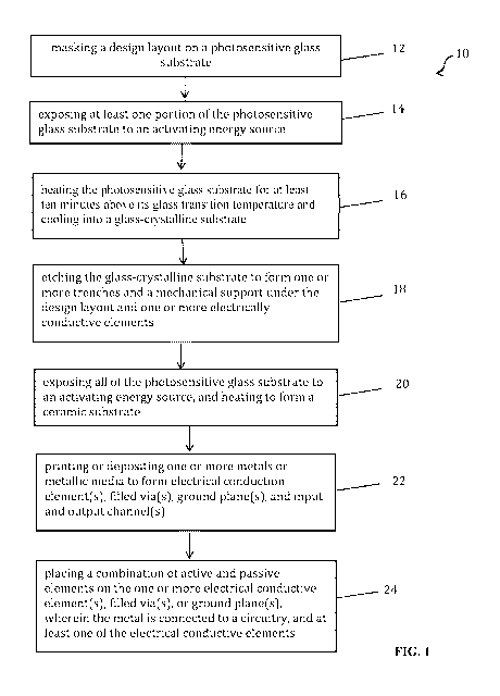
[0010] FIG. 1 is a flowchart of one method of the present invention.
DETAILED DESCRIPTION OF THE INVENTION
[0011] While the making and using of various embodiments of the present
invention are
discussed in below, it should be appreciated that the present invention
provides many
applicable inventive concepts that can be embodied in a wide variety of
specific contexts.
The specific embodiments discussed herein are merely illustrative of specific
ways to make
and use the invention and do not delimit the scope of the invention.
[0012] To facilitate the understanding of this invention, a number of terms
are defined below.
Terms defined herein have meanings as commonly understood by a person of
ordinary skill
in the areas relevant to the present invention. Terms such as "a", "an" and
"the" are not
intended to refer to only a singular entity, but include the general class of
which a specific
example may be used for illustration. The terminology herein is used to
describe specific
embodiments of the invention, but their usage does not limit the invention,
except as outlined
in the claims. The ceramic moves Tg up 200 C to 650 C.
[0013] In one embodiment, the present invention includes a method of making a
mechanically and thermally stabilized PCB substrate. The printed circuit board
(PCB) device
will be mechanically and thermally stabilized. Where the PCB substrate is made
on a
photosensitive glass substrate, as described herein, it is generally formed
by; exposing at least
one portion of the photosensitive glass substrate to an activating energy
source; heating the
photosensitive glass substrate for at least ten minutes above its glass
transition temperature;
cooling the photosensitive glass substrate to transform at least part of the
exposed glass to a
CA 03156811 2022-04-01
WO 2021/076355
PCT/US2020/054394
6
crystalline material to form a glass-crystalline substrate; etching the glass-
crystalline
substrate with an etchant; flood exposing all of remaining photosensitive
glass substrate to an
activating energy source; heating the photosensitive glass substrate for at
least ten minutes
above its glass transition temperature to form a ceramic substrate; cooling
the photosensitive
glass/ceramic substrate to transform the exposed glass to a crystalline
material to form a
glass-crystalline substrate; coating the one or more electrical conductive
elements, ground
plane and input and output channels with one or more metals, wherein the metal
is connected
to a circuitry. The mechanically and thermally stabilized PCB can be used for
circuitry
including DC, RF, millimeter wave (mm wave), and terahertz frequencies. The
thermal
expansion coefficient of the ceramic substrate, as measured linearly, is
between 7.5 and 10 a,
and in some cases is greater than 7.2, or is 7.4, 7.5, 8.0, 8.5, 9.0, 9.5, 10,
10.4, or less than
10.5. In one particular example, the step of heating the substrate above its
glass transition
temperature (Tg) is applied for one or more process cycles to increase the Tg
of the substrate
where each processing cycle increases the Tg by a minimum of 50 C to a maximum
of
650 C.
[0014] In one embodiment, the one or more metals are selected from Fe, Cu, Au,
Ni, In, Ag,
Pt, or Pd for the metallization. For higher temperature applications Pt and/or
Pd can be used
as the metallization. In another aspect, the metallization connects to the
circuitry through a
surface a buried contact, a blind via, a glass via, a straight-line contact,
rectangular contact, a
polygonal contact, or a circular contact.
[0015] In another aspect, the photosensitive glass substrate is a glass
substrate comprising a
composition of: 60 - 76 weight % silica; at least 3 weight % 1(20 with 6
weight % - 16 weight
% of a combination of 1(20 and Na2O; 0.003-1 weight % of at least one oxide
selected from
the group consisting of Ag2O andAu20; 0.003-2 weight % Cu2O; 0.75 weight % - 7
weight
%B203, and 6 - 7 weight % A1203; and the combination of B203; and A1203 not
exceeding 13
weight %; 8-15 weight % Li2O; and 0.001 ¨ 0.1 weight % Ce02. In another
aspect, the
photosensitive glass substrate is a glass substrate comprising a composition
of: 35 - 76 weight
% silica, 3- 16 weight % 1(20, 0.003-1 weight % Ag20, 8-15 weight % Li2O, and
0.001 ¨ 0.1
weight % Ce02. In another aspect, the photosensitive glass substrate is at
least one of: a
photo-definable glass substrate comprises at least 0.1 weight % Sb203 or
As203; a photo-
definable glass substrate comprises 0.003-1 weight % Au20; a photo-definable
glass substrate
comprises 1-18 weight % of an oxide selected from the group consisting of CaO,
ZnO, Pb0,
Mg0, Sr0 and Ba0; and optionally has an anisotropic- etch ratio of exposed
portion to said
CA 03156811 2022-04-01
WO 2021/076355
PCT/US2020/054394
7
unexposed portion is at least one of 10-20:1; 21-29:1; 30- 45:1; 20-40:1; 41-
45:1; and 30-
50:1. In another aspect, the photosensitive glass substrate is a
photosensitive glass ceramic
composite substrate comprising at least one of silica, lithium oxide, aluminum
oxide, or
cerium oxide. In another aspect, the electronic circuit. In another aspect,
the method further
comprises forming the mechanically and thermally stabilized transmission line
structure into
a feature of at least one or more passive and active components to form
bandpass, low pass,
high pass, shunt or notch filter and other circuits.
[0016] The present invention relates to creating a high temperature
replacement printed
circuit board (PCB) substrate using a sapphire substrates using thin film
additive processes on
semiconductor, insulating or conductive substrates is expensive with low yield
and a high
variability in performance. An example of additive micro-transmission can be
seen in articles
Semiconductor Microfabrication Processes by Tian et al. rely on expensive
capital
equipment; photolithography and reactive ion etching or ion beam milling tools
that generally
cost in excess of one million dollars each and require an ultra-clean, high-
production silicon
fabrication facility costing millions to billions more. This invention
provides a cost effective
ceramic electronic individual device, or as an array of passive devices, for a
uniform response
for DC, RF, millimeter wave (mm wave) and terahertz frequencies.
[0017] Microstructures have been produced relatively inexpensively with these
glasses using
conventional semiconductor processing equipment. In general, glasses have high
temperature
stability, good mechanical and electrical properties, and have better chemical
resistance than
plastics and many metals. Photoetchable glass is comprised of lithium-aluminum-
silicate
glass containing traces of silver ions. When exposed to UV-light within the
absorption band
of cerium oxide, the cerium oxide acts as sensitizers, absorbing a photon and
losing an
electron that reduces neighboring silver oxide to form silver atoms, e.g.,
ce3+ Ag+ ce4+ Ago
[0018] The silver atoms coalesce into silver nanoclusters during the baking
process and
induce nucleation sites for crystallization of the surrounding glass. If
exposed to UV light
through a mask, only the exposed regions of the glass will crystallize during
subsequent heat
treatment.
[0019] This heat treatment must be performed at a temperature near the glass
transformation
temperature (e.g., greater than 465 C. in air). The crystalline phase is more
soluble in
etchants, such as hydrofluoric acid (HF) than the unexposed vitreous,
amorphous regions.
CA 03156811 2022-04-01
WO 2021/076355
PCT/US2020/054394
8
The crystalline regions etched greater than 20 times faster than the amorphous
regions in
10%HF, enabling microstructures with wall slopes ratios of about 20:1 when the
exposed
regions are removed. See T.R. Dietrich, et al., "Fabrication Technologies for
Microsystems
utilizing Photoetchable Glass", Microelectronic Engineering 30,497 (1996),
relevant portions
of which are incorporated herein by reference.
[0020] The exposed portion may be transformed into a crystalline material by
heating the
glass substrate to a temperature near the glass transformation temperature.
When etching the
glass substrate in an etchant such as hydrofluoric (HF) acid, the anisotropic-
etch ratio of the
exposed portion to the unexposed portion is at least 30:1, when the glass is
exposed to a
broad spectrum mid-ultraviolet (about 308-312nm) flood lamp to provide a
shaped glass
structure that has an aspect ratio of at least 30:1, and to provide a lens
shaped glass structure.
The exposed glass is then baked typically in a two-step process. Temperature
range heated
between of 420 C-520 C for between 10 minutes to 2 hours. For the coalescing
of silver ions
into silver nanoparticles the temperature range for heating is between 520 C-
620 C for
between 10 minutes and 2 hours allowing the lithium oxide to form around the
silver
nanoparticles. The glass plate is then etched. The glass substrate is etched
in an etchant of HF
solution, typically 5% to 10% by volume, where in the etch ratio of exposed
portion to that of
the unexposed portion is at least 30:1. The etched features created can be
filled with metals,
dielectrics, and/or resistive elements and combined with, or connected to,
active devices to
form circuits. The final processing steps prior to the creation of the
electric circuits and
structures in photoetchable glass structure is to fully convert the remaining
glass substrate to
a ceramic phase. The ceramicization of the glass is accomplished by exposing
all of the
remaining photodefinable glass substrate to approximately 20J/cm2 of 310 nm
light. Then the
substrate is heated to a temperature to between 420 C-520 C for up to 2 hours.
In one
particular example, the step of heating the substrate above its glass
transition temperature
(Tg) is applied for one or more process cycles to increase the Tg of the
substrate where each
processing cycle increases the Tg by a minimum of 50 C to a maximum of 650 C.
For the
coalescing of silver ions into silver nanoparticles the temperature range for
heating is
between 520 C-620 C for between 10 minutes and 2 hours, which allows lithium
oxide to
form around the silver nanoparticles. The substrate is then cooled and then
processed to add
metalized structures (interconnects, via and others). Finally the active and
passive devices
are placed on to the ceramitized substrate. The Tg of the photodefinable glass
can be
increased through the exposure and thermal cycling from 200 C to 650 C. 200 C
is the Tg
CA 03156811 2022-04-01
WO 2021/076355
PCT/US2020/054394
9
for the un-exposed nanocrystalline photodefinable glass ceramic material. On
full cycle
increases the Tg to 600 C. Subsequent thermal and photo exposures can increase
the Tg to
650 C. This increase requires a minimum of two exposures,
[0021] The present invention includes a method of making a mechanically and
thermally
stabilized high temperature printed circuit board (PCB) comprising, consisting
essentially of,
or consisting of: masking a design layout comprising one or more structures
that form one or
more structures on a photosensitive glass substrate; exposing at least one
portion of the
photosensitive glass substrate to an activating energy source; heating the
photosensitive glass
substrate for at least ten minutes above its glass transition temperature;
cooling the
photosensitive glass substrate to transform at least part of the exposed glass
into a glass-
crystalline substrate; etching the glass-crystalline substrate with an etchant
solution to form
one or more trenches and a mechanical support under the design layout and one
or more
transmission line structures with electrical conduction elements; flood
exposing all of the
photosensitive glass substrate to an activating energy source; heating the
photosensitive glass
substrate for at least ten minutes above its glass transition temperature to
form a ceramic
substrate; printing or depositing one or more metals or metallic media that
form the one or
more electrical conduction elements, one or more filled vias, a ground plane,
and one or more
input and output channels; and placing a combination of active and passive
elements on the
one or more electrical conductive elements, filled via, or ground plane,
wherein the metal is
connected to a circuitry, and at least one of the electrical conductive
elements.
[0022] The present invention also includes a method of making a mechanically
and thermally
stabilized high temperature printed circuit board (PCB) comprising, consisting
essentially of,
or consisting of: exposing at least one portion of the photosensitive glass
substrate previously
masked with a design layout to an activating energy source; heating the
photosensitive glass
substrate for at least ten minutes above its glass transition temperature;
cooling the
photosensitive glass substrate to transform at least part of the exposed glass
into a glass-
crystalline substrate; etching the glass-crystalline substrate with an etchant
to form one or
more trenches and a mechanical support under the design layout and one or more
electrical
conduction elements; exposing the entire photosensitive glass substrate to an
activating
energy source; heating the photosensitive glass substrate for at least ten
minutes above its
glass transition temperature to form a ceramic substrate; printing or
depositing one or more
metals or metallic media that form the one or more electrical conduction
elements, one or
more filled vias, a ground plane, and one or more input and output channels;
and placing a
CA 03156811 2022-04-01
WO 2021/076355
PCT/US2020/054394
combination of active and passive elements on the one or more electrical
conductive
elements, filled via, or ground plane, wherein the metal is connected to a
circuitry, and at
least one of the electrical conductive elements.
[0023] FIG. 1 is a flowchart 10 that shows one method of making a mechanically
and
5 thermally stabilized high temperature printed circuit board (PCB). In
step 12, the step is
masking a design layout comprising one or more structures that form one or
more structures
on a photosensitive glass substrate. In step 14, the step is exposing at least
one portion of the
photosensitive glass substrate to an activating energy source. In step 16, the
step is heating
the photosensitive glass substrate for at least ten minutes above its glass
transition
10 .. temperature followed by cooling the photosensitive glass substrate to
transform at least part
of the exposed glass into a glass-crystalline substrate. In step 18, the step
is etching the glass-
crystalline substrate with an etchant solution to form one or more trenches
and a mechanical
support under the design layout and one or more transmission line structures
with electrical
conduction elements. In step 20, the step is exposing all of the
photosensitive glass substrate
to an activating energy source, e.g., by flood exposing the substrate and
heating the
photosensitive glass substrate for at least ten minutes above its glass
transition temperature to
form a ceramic substrate. In step 22, the step is printing or depositing one
or more metals or
metallic media that form the one or more electrical conduction elements, one
or more filled
vias, a ground plane, and one or more input and output channels. Finally, in
step 24, the step
is and placing a combination of active and passive elements on the one or more
electrical
conductive elements, filled via, or ground plane, wherein the metal is
connected to a circuitry,
and at least one of the electrical conductive elements.
[0024] It will be understood that particular embodiments described herein are
shown by way
of illustration and not as limitations of the invention. The principal
features of this invention
can be employed in various embodiments without departing from the scope of the
invention.
Those skilled in the art will recognize, or be able to ascertain using no more
than routine
experimentation, numerous equivalents to the specific procedures described
herein. Such
equivalents are considered to be within the scope of this invention and are
covered by the
claims.
.. [0025] All publications and patent applications mentioned in the
specification are indicative
of the level of skill of those skilled in the art to which this invention
pertains. All
publications and patent applications are herein incorporated by reference to
the same extent
CA 03156811 2022-04-01
WO 2021/076355
PCT/US2020/054394
11
as if each individual publication or patent application was specifically and
individually
indicated to be incorporated by reference.
[0026] The use of the word "a" or "an" when used in conjunction with the term
"comprising"
in the claims and/or the specification may mean "one," but it is also
consistent with the
meaning of "one or more," "at least one," and "one or more than one." The use
of the term
"or" in the claims is used to mean "and/or" unless explicitly indicated to
refer to alternatives
only or the alternatives are mutually exclusive, although the disclosure
supports a definition
that refers to only alternatives and "and/or." Throughout this application,
the term "about" is
used to indicate that a value includes the inherent variation of error for the
device, the method
being employed to determine the value, or the variation that exists among the
study subjects.
[0027] As used in this specification and claim(s), the words "comprising" (and
any form of
comprising, such as "comprise" and "comprises"), "having" (and any form of
having, such as
"have" and "has"), "including" (and any form of including, such as "includes"
and "include")
or "containing" (and any form of containing, such as "contains" and "contain")
are inclusive
or open-ended and do not exclude additional, unrecited elements or method
steps. In
embodiments of any of the compositions and methods provided herein,
"comprising" may be
replaced with "consisting essentially of' or "consisting of'. As used herein,
the phrase
"consisting essentially of' requires the specified integer(s) or steps as well
as those that do
not materially affect the character or function of the claimed invention. As
used herein, the
term "consisting" is used to indicate the presence of the recited integer
(e.g., a feature, an
element, a characteristic, a property, a method/process step or a limitation)
or group of
integers (e.g., feature(s), element(s), characteristic(s), property(ies),
method/process steps or
limitation(s)) only.
[0028] The term "or combinations thereof' as used herein refers to all
permutations and
combinations of the listed items preceding the term. For example, "A, B, C, or
combinations
thereof' is intended to include at least one of: A, B, C, AB, AC, BC, or ABC,
and if order is
important in a particular context, also BA, CA, CB, CBA, BCA, ACB, BAC, or
CAB.
Continuing with this example, expressly included are combinations that contain
repeats of
one or more item or term, such as BB, AAA, AB, BBC, AAABCCCC, CBBAAA, CABABB,
and so forth. The skilled artisan will understand that typically there is no
limit on the number
of items or terms in any combination, unless otherwise apparent from the
context.
CA 03156811 2022-04-01
WO 2021/076355
PCT/US2020/054394
12
[0029] As used herein, words of approximation such as, without limitation,
"about",
"substantial" or "substantially" refers to a condition that when so modified
is understood to
not necessarily be absolute or perfect but would be considered close enough to
those of
ordinary skill in the art to warrant designating the condition as being
present. The extent to
which the description may vary will depend on how great a change can be
instituted and still
have one of ordinary skill in the art recognize the modified feature as still
having the required
characteristics and capabilities of the unmodified feature. In general, but
subject to the
preceding discussion, a numerical value herein that is modified by a word of
approximation
such as "about" may vary from the stated value by at least 1, 2, 3, 4, 5, 6,
7, 10, 12 or 15%.
[0030] All of the compositions and/or methods disclosed and claimed herein can
be made
and executed without undue experimentation in light of the present disclosure.
While the
compositions and methods of this invention have been described in terms of
preferred
embodiments, it will be apparent to those of skill in the art that variations
may be applied to
the compositions and/or methods and in the steps or in the sequence of steps
of the method
described herein without departing from the concept, spirit and scope of the
invention. All
such similar substitutes and modifications apparent to those skilled in the
art are deemed to
be within the spirit, scope and concept of the invention as defined by the
appended claims.
[0031] To aid the Patent Office, and any readers of any patent issued on this
application in
interpreting the claims appended hereto, applicants wish to note that they do
not intend any of
the appended claims to invoke paragraph 6 of 35 U.S.C. 112, U.S.C. 112
paragraph (f), or
equivalent, as it exists on the date of filing hereof unless the words "means
for" or "step for"
are explicitly used in the particular claim.
[0032] For each of the claims, each dependent claim can depend both from the
independent
claim and from each of the prior dependent claims for each and every claim so
long as the
prior claim provides a proper antecedent basis for a claim term or element.