Note: Descriptions are shown in the official language in which they were submitted.
WO 2021/105172 1
PCT/EP2020/083300
A working electrode for a photovoltaic device, and a photovoltaic device
including the
working electrode
Technical field
The present invention relates to a working electrode comprising a light
absorbing layer for use
in a photovoltaic device. The present invention also relates a photovoltaic
device including the
working electrode.
Background
Photovoltaic devices provide conversion of light into electricity using
semiconducting
materials that exhibit a photovoltaic effect.
A photovoltaic device, such as a solar cell, is a device which directly
converts sunlight into
electricity. Light incident on the surface of the photovoltaic device produces
electric power. A
photovoltaic device comprises a working electrode including a light absorbing
layer. The light
absorbing layer comprises a light absorbing photovoltaic material, which has
the ability to
absorb light, and to generate photo-excited electrons. When the energy of a
photon is equal
to or greater than the bandgap of the light absorbing material, the photon is
absorbed by the
material and a photo-excited electron is generated.
The energy of photons depends on the type of light source. For example, the
energy of
photons of indoor light is less than the energy of photons of sun light.
Further, the energy of
photons from the outdoor sun light depends on the latitude. If the energy of
the photons
reaching the light absorbing material is less than the bandgap of the light
absorbing material,
the photons cannot be absorbed by the material and thus the energy cannot be
converted
into electricity. If the energy of the photons reaching the light absorbing
material is equal to
or larger than the bandgap of the light absorbing material, the photons are
absorbed by the
material, but only the amount of energy corresponding to the bandgap is
converted into
electricity. Thus, it is important that the light absorbing material in the
photovoltaic device
has a bandgap that matches the light source that the device will be using.
Accordingly, it is a desire to be able to tune the bandgap of the light
absorbing photovoltaic
material to allow efficient light energy to electric energy conversion of a
light spectrum from
weak light sources, such as indoor light as well as from outdoor sun light.
Today, silicon is the most commonly used light absorbing photovoltaic material
in solar cells.
Silicon has several advantages, for example, it is chemically stable and
environmentally
friendly. Silicon provides efficient light energy to electric energy
conversion of sun light.
However, silicon is less efficient for conversion of weak light sources.
It is also known to use dye molecules as the light absorbing photovoltaic
material in solar cells.
Such solar cells are called dye-sensitized solar cells (DSSC). In DSSC solar
cells, the light
absorbing layer comprises a semiconducting scaffolding layer comprising a net
of sintered
particles, such as metal oxide particles, for example TiO2 particles, dyed
with a light adsorbing
dye. Light absorbing dyes are also called sensitizing dyes. The dye molecules
are disposed on
CA 03156886 2022-5-2
WO 2021/105172 2
PCT/EP2020/083300
the surface of the semiconducting particles. The dye absorbs the incident
light and uses the
energy in the light to excite electrons. The semiconducting particles serve as
a material for
transportation of the excited electrons to a conductive layer.
A dye-sensitized solar cell is described in EP2533352. In EP2533352 a porous
semi-conductor
layer is placed on a porous conductive metal layer that serves as current
collector electrode.
The porous semi-conductor layer absorbs a dye. The dye molecules will attach
to the surface
of the porous semi-conductor layer. The porous semi-conductor layer has a
double function
and acts as a scaffolding structure for holding the dye molecules spread out
in a 3 dimensional
structure. The other function is for the semi-conducting layer to transfer
excited electrons (or
holes) to the current collector. In EP2533352 is further described that due to
the metallic
properties of the current collector high conversion efficiency can be obtained
even if the
thickness of the porous semi-conductive layer is made thicker than 14 gm (a
thicker semi-
conducting layer can absorb more dye). A few common dyes such as ruthenium
dye,
phthalocyanine dye or cyanine dye are referred to in EP2533352.
Another configuration of a dye-sensitized solar cell is described in
EP2834823, where a dye-
sensitized solar cell including a working electrode, a porous insulating
layer, a porous first
conducting metal layer formed on top of the porous insulating layer and
arranged in electrical
and physical contact with the light absorbing layer, a counter electrode
including a second
conducting metal layer, and a conducting medium in the form of a liquid
electrolyte for
transferring charges between the counter electrode and the working electrode.
The working
electrode comprises a porous TiO2 layer deposited onto the first conductive
layer. Dye
molecules are absorbed onto the surface of the TiO2 particles of the TiO2
layer in a
conventional manner.
The dye molecules preferably form a monolayer of dye molecules on the
particles of the
scaffolding semi-conducting structure. To ensure sufficient light absorption,
there should be
a certain amount of sensitizing dye in the light absorbing layer. The number
of molecules per
cm2 needed to achieve sufficient light absorption depends on the absorption
coefficient of the
dye. To achieve enough sensitizing dye in the light absorbing layer, the light
absorbing layer
normally includes several hundreds of layers of dyed semiconducting particles.
The number
of layers will determine the thickness of the light absorbing layer and
increasing the amount
of sensitizing dye will increase the thickness of the light absorbing layer.
Thus, a problem with
dye-sensitized solar cells is that in order to increase the amount of dye the
porous
semiconductor layer becomes thicker. A thick semi-conducting layer will reduce
the efficiency
of the solar cell due to longer electron diffusion lengths.
A number of documents, for example KR101469570, JP2016207919, describe various
methods
for preventing agglomeration of dye molecules in the semi-conducting layer of
a dye-
sensitized solar cell. Aggregations on the semi-conductor surfaces are
described to be
hindering the efficiency of the DSSCs.
CA 03156886 2022-5-2
WO 2021/105172 3
PCT/EP2020/083300
Lei Zhang et al, "Dye aggregation in dye-sensitized solar cells", Journal of
materials chemistry
A, vol. 5, no. 37, 5 September 2017, discloses a review regarding aggregation
of dyes coated
on TiO2 in solar cells. On page 19542, 2"d , it especially mentions that dye
aggregates severely
disrupt the function of the DSSC device and that dye aggregation can affect
the photovoltaic
DSSC performance. Dye aggregation in DSSCs is most comely regarded as a
phenomenon that
is best to be avoided.
Another type of solar cell is described in W02018/021952. A plurality of
grains of a doped
semi-conducting material in electrical contact with a conducting layer and the
grains being at
least partly surrounded by a charge conducting material, like PEDOT, is
described. The grains
are described to be made of silicon or alternatively of CdTe, CIGS, CIS, GaAs,
or a perovskite.
In recent years, there has been an increasing interest in organic sensitizing
dyes for usage in
dye-sensitized solar cells (DSSCs) since it has been found that organic dyes
in combination with
ion-based electrolytes improve the performance of DSSC devices, in particular
for indoor
applications. There exist a large number of different types of sensitizing
dyes with different
abilities to absorb light.
Summary
It is an aim of the present invention to at least partly overcome some of the
above-mentioned
problems and to provide an improved working electrode for a photovoltaic
device, and an
improved photovoltaic device including the working electrode.
This aim is achieved with a working electrode as defined in claim 1.
The working electrode for a photovoltaic device comprises a light absorbing
layer and a
conductive layer arranged in electrical contact with the light absorbing layer
and the light
absorbing layer comprises a light absorbing photovoltaic material consisting
of a plurality of
dye molecules. The light absorbing layer if formed by a layer of a plurality
of clusters, whereby
each cluster is formed by dye molecules and each dye molecule in a cluster is
bonded to its
adjacent dye molecules.
The dye molecules form a plurality of clusters of dye molecules. The clusters
form a light-
absorbing layer, which layer is in electrical contact with the conductive
layer. The separate
layer of clusters is not dispersed onto a scaffolding layer of a semi-
conducting material.
By arranging the dye molecules into clusters that form a separate light-
absorbing layer, the
semi-conducting scaffolding layer of the conventional dye-sensitized solar
cell can be omitted.
Thus, the solar cell comprising a light-absorbing layer of clusters can be
made thinner than the
conventional dye-sensitized solar cell for the same amount of dye molecules.
The light absorbing layer does not contain dye molecules disposed or absorbed
on surfaces of
semiconducting particles. The dye molecules forming clusters are not disposed
on
semiconducting particles within a semiconducting layer. The clusters can be
directly stacked,
without support of a semiconducting scaffolding layer, on the surface of a
conducting layer,
CA 03156886 2022-5-2
WO 2021/105172 4
PCT/EP2020/083300
thus forming a working electrode of a solar cell that can be directly
connected to an external
circuit.
In omitting the step where a dye is absorbed by a semi-conducting layer in
preparation of a
dye-sensitized solar cell, the production time of a solar cell is
significantly reduced_ Absorption
of the dye can readily take several hours to complete. A further reduction of
the production
time is achieved by not having to form the semi-conducting scaffolding layer
in producing the
dye-sensitized solar cell.
Another advantage of having a light absorbing layer as a separate layer of
clusters of dye
molecules is that more dye molecules per square meter can be inserted compare
to a dye-
sensitized solar cell having the dye molecules absorbed by a semi-conducting
layer.
The solar cell comprising a working electrode having a light absorbing layer
made of clusters
of dye molecules, where the clusters form a separate layer, can be made
thinner than a dye-
sensitized solar cell comprising a dye infused semi-conducting scaffolding
layer. A thinner solar
cell has many advantages. A shorter distance between the electrodes of the
solar cell increase
the efficiency of the solar cell. A thinner solar cell may also find new
applications where it
desirable to have a thin and light-weight solar cell.
A cluster of dye molecules is formed by arranging the dye molecules in a
crystal lattice or in a
random, amorphous structure, or a combination thereof. By the term "crystal
lattice" is meant
that the cluster has a defined and repeatable arrangement of the dye
molecules.
A dye molecule within the cluster is bonded to its adjacent dye molecules. The
bond between
the dye molecules can be electrostatic bonds, or covalent bonds, or van der
Waal bonds, and
the like.
The term "dye" shall be understood to refer to dyes that exhibit a
photovoltaic effect, i.e. have
the ability to absorb light, and to generate photo-excited electrons.
The dye molecules of the cluster can be dye molecules of different chemical
composition. The
amount of dye per volume needed in the light absorbing layer depends on the
type of dye
since different dyes have different absorptions coefficients, and accordingly
their ability to
absorb light is different. The size of the clusters can be controlled during
the manufacturing
of the clusters. Thus, it is possible to produce clusters of different sizes
depending on the
amount of dye needed in the light absorbing layer in order to absorb the
incoming light
efficiently. If the clusters are made large enough, there is only need of one
single layer of
clusters to achieve the same effect as in the prior art dye-sensitized solar
cells. Thus, the light
absorbing layer of the invention can be made significantly thinner.
In the past decades, several thousands of different dyes have been synthesised
and tested in
MSC devices. Known dye molecules can be used for forming clusters and
crystalline clusters
with a bandgap that differs from the HOMO/LUMO gap of the single dye
molecules. This
makes it possible to produce light absorbing layer with different bandgaps.
For example, it is
possible to produce clusters with bandgaps in the interval of 1.0 - 1.6 eV.
Thus, it is possible
CA 03156886 2022-5-2
WO 2021/105172 5
PCT/EP2020/083300
to optimize the bandgap of the light absorbing layer of the photovoltaic
device with regards
to the specific light spectrum that is to be converted into electricity.
In one aspect, a mixture of two or more dyes is used in the clusters of the
light absorbing layer.
In one aspect, spaces are formed between the clusters, and the working
electrode comprises
a conducting medium that fills the spaces between the clusters in the light
absorbing layer.
The conducting medium transfers charges to/from the clusters in the working
electrode.
In one aspect, the clusters forming the light absorbing layer is essentially a
monolayer of
clusters. The clusters absorb the incident light and uses the energy in the
light to excite
electrons. In this aspect, the clusters are arranged in a single layer so that
each of the clusters
directly faces unrestricted incident light. With unrestricted incident light
is meant that the
light is coming directly from the source of light, such as the sun or a lamp,
and the light is not
obscured by other clusters disposed on top of the clusters in the single
layer. It is
is advantageous to have a single layer of cluster since each
cluster will face the incident light and
will contribute to the conversion of the incident light into electricity. If
the light absorbing
layer comprises more than one layer of clusters arranged on top of each other,
the clusters in
the upper layers will obscure the clusters in the lower layers so that they
will not contribute
as much to the light conversion. Further, if the light absorbing layer has
only one single layer
of clusters, the thickness of the light absorbing layer can be reduced. The
thickness of the light
absorbing layer is substantially equal to the thickness of the clusters in the
single layer of
clusters.
In one aspect, at least 40% of the clusters forming the light absorbing layer
are crystalline
clusters, where the dye molecules within the clusters are arranged in a
defined and repeatable
way, and preferably at least 50% of the clusters are crystalline clusters, and
most preferably
at least 70% of the clusters are crystalline clusters.
The clusters with a crystalline structure or at least a partly crystalline
structure of dye
molecules, hereinafter called crystalline clusters, have some specific
advantages. The
properties of the single dye molecules change when the dye molecules are
arranged into a
crystal. For example, the single dye molecules have a HOMO/LUMO gap. However,
a
crystalline cluster has a bandgap that depends on the type of dye molecules in
the cluster. A
smaller bandgap, compared to the HOMO/LUMO gap, will broaden the light
absorption
spectrum of the crystalline cluster, as compared to single dye molecules. A
broader light
absorption spectrum means that the crystalline cluster has a capability to
absorb light in a
broader wavelength range, as compared to the single dye molecules. The light
harvesting
capability is thereby increased for the crystalline cluster compared to a
structure in which the
same amount and type of dye molecules are arranged as single molecules
absorbed in a
scaffolding structure.
CA 03156886 2022-5-2
WO 2021/105172 6
PCT/EP2020/083300
In a working electrode where the light absorbing layer comprise crystalline
clusters, at least
40%, 45% or 50% of the cluster shall be crystalline clusters. Preferably, at
least 70% or 80% of
the clusters in the light absorbing layer shall be crystalline clusters, and
most preferably, at
least 90% of the clusters are crystalline clusters.
An advantage of crystalline clusters in addition to the advantages listed
above is the possibility
to design solar cells with specific light absorption spectrum. This enables
the solar cell to be
tailor-made for a specific use having specific light conditions. The
possibility to have different
types of dye molecules in a crystalline cluster will further enhance the
flexibility of designing
a solar cell.
In some aspects, the conductive layer is in direct physical and electrical
contact with the light
absorbing layer. This means that at least some of the clusters are in physical
contact with the
conductive layer.
In some aspects, the clusters forming the light absorbing layer are in
physical and electrical
contact with the conductive layer and the clusters are bonded to the
conductive layer. The
light absorbing layer is arranged in electrical contact with a conductive
layer so that the
conductive layer receives photo-generated chargers from the clusters. In an
embodiment
where the clusters are in direct physical and electrical contact with the
conductive layer, the
clusters are bonded to the conductive layer. The clusters within the light
absorbing layer need
not be bonded to each other.
In one aspect, the clusters are arranged in a single layer along the
conductive layer, and each
cluster is in physical and electrical contact with the conductive layer.
The conductive layer is preferably a porous layer of sintered metallic
particles. The particles
may also be other types of conductive particles, like particles of conducting
glass, carbon or
semi-conducting materials.
In some aspects, at least 80% of the clusters comprise more than 100 dye
molecules per
cluster. Preferably, the at least 80% of the clusters comprise more than 1000
dye molecules
per cluster. Most preferably, at least 80% of the clusters comprise more than
10 000 dye
molecules per cluster. Thus, the light absorbing layer will contain sufficient
amounts of dye to
absorb a substantial part of the incoming light for conversion to electricity
for most types of
dye.
A sufficiently large number of dye molecules ensures sufficient light
absorption. The larger the
number of dye molecules, the better light absorption is achieved. To achieve
the same light
absorption as the known dye-sensitized solar cells, the light absorbing layer
should contain
roughly the same number of dye molecules per unit surface area as the known
dye-sensitized
solar cells. lithe clusters contain a smaller number of molecules, the light
absorbing layer may
contain more than one layer of clusters to ensure that the light absorbing
layer will contain
CA 03156886 2022-5-2
WO 2021/105172 7
PCT/EP2020/083300
sufficient amounts of dye. The larger the clusters, the less number of cluster
layers of are
needed in the light absorbing layer.
In some aspects, the size of at least 80% of the clusters having more than 100
dye molecules
is more than 5 nm along a straight line through a cluster connecting two
points on the surface
of the cluster. The straight line is, for example, the diameter of a round
cluster or the z-axis of
a cubic lattice of a crystalline cluster.
For larger clusters the size of at least 80% of the clusters can be more than
10 nm along a
straight line through the cluster connecting two points on the surface of the
cluster. Most
preferably, the size of at least 80% of the clusters is more than 20 nm along
a straight line
through the cluster connecting two points on the surface of the cluster. The
desired size of
the clusters depends on the type of dye and its absorptions coefficient. The
larger size of the
clusters, the better the light absorption.
In some aspects for larger clusters, the size of at least 80% of the clusters
is less than 2 gm
along a straight line through a cluster connecting two points on the surface
of the cluster.
Preferably, the size of at least 80% of the clusters is less than 1 pm. Thus,
the thickness of the
light absorbing layer will be thin. The thickness of the light absorbing layer
depends on the
size of the cluster. The light absorbing layer is essentially a monolayer of
clusters. For a the
light absorbing layer containing one single layer of clusters, the thickness
of the light absorbing
layer is substantially equal to the thickness of the clusters.
Suitably, the size of at least 80% of the clusters is between 5 nm and 2 pm at
a straight line
connecting two points on the surface of the cluster. Preferably, the size of
at least 80% of the
clusters is between 10 nm and 1 pm at a straight line connecting two points on
the surface of
the cluster. Thus, the light absorbing layer can be designed to contain
sufficient amounts of
dye to absorb a substantial part of the incoming light of various light
conditions for conversion
to electricity, and the light absorbing layer will be thin.
According to some aspects, the dye molecules are organic dye molecules,
organometallic dye
molecules or natural dye molecules.
In one aspect, the dye is selected from a group comprising or consisting of
organic dyes such
as tetrahydroquinolines, pyrolidine, diphenylamine, triphenylamine (WA),
coumarin dyes,
indole dyes, aryl amine dyes, porphyrine dyes, fluorine dyes, carbazole dyes
(CBZ),
phenothiazine dyes (PTZ), phenoxazine dyes (POZ), hemicyanine dyes,
merocyanine dyes,
squaraine dyes, perylene dyes, anthraquinone dyes, boradiazaindacene (BODIPY)
dyes,
oligothiophene dyes, and polymeric dyes, and fluorinated quinoxa line dyes. It
has been found
that organic dyes can improve the performance of DSSC devices. By using
clusters of crystalline
CA 03156886 2022-5-2
WO 2021/105172 8
PCT/EP2020/083300
organic dyes, the band gap can be reduced resulting in light absorption in a
broader
wavelength range and more efficient light absorption of longer wavelengths of
light.
In another aspect, the dye is selected from a group comprising or consisting
of natural dyes
such as betalain dyes, anthocyanin dyes [268], chlorophyll dyes [269],
flavonoid dyes [270],
and carotenoid dyes.
Metal organic dyes are well known photovoltaic materials having good light
absorption and
which are tailor made for efficient absorption of visible light. Examples of
organometallic dyes
can be the commonly used dyes of ruthenium (Flu) bipyridyl derivatives (N3:
cis-
di isothiocyanato-bis(2,21-bipyridy1-4,4'-dicarboxylic
acid) ruthenium(II); N719: di-
tetrabutylammonium
cis-
bis(isothiocyanato)bis(2,2'-bipyridy1-4,4'-dicarboxylato)
ruthenium(10; Z907: cis-bis(isothiocyanato)(2,2'-bipyridy1-4,4'-
dicarboxylato)(4,4'-di-nonyl-2'-
bipyridyl).
In a third aspect, the dye is selected from a group comprising or consisting
of organometallic
dye molecules, such as metal organic complexes, for example, rutheniumbased
complexes or
other metal complexes such as iron complexes or platinum complexes.
Other types of dyes can be metal-free organic dyes, like for example eosin Y,
aniline blue,
bromophenol blue, alcian blue, methyl orange, crystal violet, fast green, and
carbol fuchsin.
Also, natural dyes like for example anthocyanin, carotenoid, flavonoid or
chlorofyll pigments
can be considered for us in a solar cell.
The dye molecules suitable for use in the present invention, is not limited to
the examples
given above.
One way of determining what dye could be suitable for a desired use in a solar
cell, is to
measure the luminescence of the dye. A light "echo" from the measurement
corresponding
to the incident light without weakening light intensity or shifting of the
light can be an
indication of the suitability of the dye.
In some aspects, the clusters may comprise a kernel or a seed of a different
material. The
clusters may contain a small kernel of another material used during
manufacturing of the
clusters to start the crystallisation process. The crystals are grown on the
seed/kernel to form
crystalline clusters. An advantage of using a kernel during the manufacturing
process is that
the clusters can be spherical and of substantially equal size. This
facilitates the manufacturing
of the light absorbing layer and makes it possible to achieve a more
homogeneous layer.
Another advantage of using a kernel is that it is possible to achieve a
narrower size distribution
CA 03156886 2022-5-2
WO 2021/105172 9
PCT/EP2020/083300
of the clusters. A narrow size distribution is useful in cases where it is
necessary to control the
size of the clusters very precisely.
In some aspects, the clusters are substantially evenly distributed in the
light absorbing layer.
This provides for an even conversion of incident light over the entire surface
of the light
absorbing layer. An even distribution of the clusters also results in a large
active surface area
for conversion of light to electricity. With evenly distributed is meant that
the number of
clusters per cm2 is the same or substantially the same over the entire area of
the light
absorbing layer. With substantially evenly distributed is meant that the
number of clusters per
cm2 may vary + 10% between different parts of the light absorbing layer.
In some aspects, the thickness of the light absorbing layer is less than or
equal to 2 gm, and
preferably less than or equal to 1 pm. The present invention provides for an
efficient light
absorbing layer with a thickness less than or equal to 2 gm. The optimal
thickness of an
efficient light absorbing layer depends both on the light absorption spectrum
of the dye and
the light emission spectrum of the light source. This improves flexibility for
the use of the
photovoltaic device, because the light absorbing layer can be designed to
obtain an optimum
balance between the light absorption spectrum of the dye and the light
emission spectrum of
the light source.
In some aspects, the thickness of the light absorbing layer is between 20 nm
and 2 pm.
In some aspects, the working electrode comprises a reflective layer arranged
on an opposite
side of the light absorbing layer with respect to the upper surface. The
reflective layer is
disposed between the light absorbing layer and the first conductive layer. The
light absorbing
layer including the clusters is arranged on top of the reflective layer. The
reflective layer
comprises semiconducting particles in electrical contact with the clusters and
the first
conductive layer. The semiconducting particles are made of a reflective
material, i.e. a
material that reflects light. The reflective layer reflects light back to the
light absorbing layer.
The semiconducting particles are attached to each other and form the
reflective layer. The
reflective layer acts as a mirror that scatters incident light back into the
light absorption layer
thereby increasing the effective absorption path length, and accordingly
increasing the light
absorption of the light absorbing layer. The light scattering effect of the
reflective layer is
wavelength dependent and the light scattering effect depends strongly on the
sizes of the
semiconducting particles in the reflective layer. Thus, the light scattering
can be tuned and
optimized by choosing semiconducting particles with adequate particle sizes to
suit the
application of the photovoltaic device at hand. The semiconducting particles
are in electrical
contact with the conductive layer as well as the light absorbing layer. Thus,
the clusters are in
electrical contact with the conductive layer via the semiconducting particles.
The semiconducting particles in the reflective layer are designed so that they
will reflect the
light. In some aspects, the size of at least 80% of the semiconducting
particles, or agglomerates
of the semiconducting particles, in the reflective layer is larger than 0.1
gm, and preferably
CA 03156886 2022-5-2
WO 2021/105172 10
PCT/EP2020/083300
larger than 0.2 rn. The larger particles the better they will reflect the
light. If the
semiconducting particles are smaller than 0.1 p.m, their ability to reflect
light is poor.
In one aspect, the size of at least 80% of the semiconducting particles is
between 0.1 Finn and
2 Rm. This will improve the light scattering ability of the semiconducting
particles.
In some aspects, the semiconducting particles are made of titanium dioxide
(TiO2). It is
advantageous to use titanium dioxide, since it reflects light well without
absorbing the light.
Titanium oxide has a high refractive index, and a bandgap sufficiently large
to avoid absorption
of light. Further, titanium dioxide is sufficiently electrically conducting so
that the reflective
layer can efficiently transfer the photoexcited charges received from the
light absorbing layer
to the conductive layer.
In some aspects, the thickness of the reflective layer is between 0.1 lam and
10 itrn. Preferably,
the thickness of the reflective layer is between 1 lam and 10 Rm. Thus, the
reflective layer is
sufficiently thin to achieve small electrical energy losses during transfer of
the photoexcited
charges from the light absorbing layer to the conductive layer.
Preferably, the reflective layer is porous to allow a conducting medium to
pass through the
reflective layer.
In some aspects, the porosity of the reflective layer is between 40% -70%. It
is important that
the reflective layer is sufficiently porous, such that the conducting medium
can form a
continuous conducting path through the pores inside the reflective layer.
In some aspects, the light absorbing layer and the reflective layer overlap,
such that a part of
the clusters are disposed in pores formed between the semiconducting
particles. An
advantage with the light absorption layer penetrating inside the reflective
layer is that the
effective light absorption path length can be increased leading to higher
light absorption.
In this case, it is particularly advantageous to use titanium dioxide (T102)
in the semiconducting
particles, since titanium dioxide is party transparent and allows light to
reach the clusters
disposed inside pores of the of the reflective layer.
The clusters that may be disposed in the pores between semiconducting
particles are
preformed clusters of dye molecules that are not dye molecules being infused
into the
semiconducting structure in order to attach to the semiconducting scaffolding
structure,
whether some of these dye molecules form agglomerates or not.
In some aspects, pore size of the reflective layer is between 10 nrn and 1
p.m. Thus, the pores
in the reflective layer are sufficiently large to accommodate both the
clusters and the
conducting medium in the pores of the reflective layer.
In another aspect, the aim of the invention is achieved by a photovoltaic
device comprising
the working electrode according to the invention.
CA 03156886 2022-5-2
WO 2021/105172 11
PCT/EP2020/083300
The photovoltaic device comprises a working electrode according to the
invention, a counter
electrode, and a conducting medium for transferring charges between the
counter electrode
and the working electrode. The photovoltaic device can be a solar cell.
In some aspects, the photovoltaic device comprises a porous insulation
substrate, wherein the
conductive layer is a porous conductive layer formed on one side of the porous
insulation
substrate. The counter electrode may further comprise a second conductive
layer arranged
on the opposite side of the porous insulation substrate. In some aspects, the
clusters are
evenly distributed on the surface of the first conductive layer.
In some aspects, the conducting medium is an ionic based electrolyte for
transferring the
photo-excited electrons from the counter electrode to the working electrode,
which can also
include gel polymer electrolytes. A hole conducting medium is also a possible
conductive
medium.
In addition to the several advantages with a photovoltaic device having a
working electrode
in accordance with the invention mentioned above , the surface of the light
absorbing layer
may also become rougher, which rougher surface increases the probability for
reflected light
to be absorbed. This in turn reduces efficiency losses due to reflections in
the surface. A
rougher surface provides for a multitude of angels towards the incident light,
the efficiency of
the photovoltaic device does not depend critically on the angle of incidence
of the light with
respect to the layer. Thus, the optical losses are reduced compared to known
dye-sensitized
solar cells.
Brief description of the drawings
The invention will now be explained more closely by the description of
different embodiments
of the invention and with reference to the appended figures.
Fig. 1 shows one example of a working electrode including a light absorbing
layer.
Fig. 2 shows another example of a working electrode including a light
absorbing layer and a
reflective layer.
Fig. 3 shows an example of a photovoltaic device including the working
electrode shown in
figure 1.
Fig. 4 shows an enlarged part of the light absorbing layer and a conductive
layer of the
photovoltaic device shown in figure 3.
Fig. 5 shows another example of a photovoltaic device including the working
electrode shown
in figure 1.
Fig. 6 shows an example of a photovoltaic device including the working
electrode shown in
figure 2.
Detailed description
Like numbers in the figures refer to like elements throughout the description.
CA 03156886 2022-5-2
WO 2021/105172 12
PCT/EP2020/083300
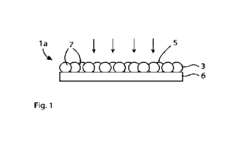
Figure 1 shows a schematic drawing of a working electrode la including a light
absorbing layer
3 made of a light absorbing photovoltaic material and a conductive layer 6 in
electrical contact
with the light absorbing layer 3. The light absorbing layer 3 has an upper
surface 5 for receiving
incoming light. The conductive layer 6 is arranged on an opposite side of the
light absorbing
layer 3 with respect to the upper surface 5. In this example, the light
absorbing layer 3 is
disposed directly on the conductive layer 6. The light absorbing photovoltaic
material consists
of a plurality of dye molecules. The dye molecules form clusters 7. The dye
molecules within
a cluster 7, are arranged so that each dye molecule is bonded to its adjacent
dye molecules.
The clusters 7 are disposed on the surface of the conductive layer 6 and
essentially every
cluster 7 is bonded to the conductive layer 6. The clusters 7 shall cover a
large part of the area
of the light absorbing layer 3 and need not be bonded to each other.
Preferably, the light
absorbing layer 3 is porous to allow a conducting medium to pass through the
light absorbing
layer. To achieve sufficient light absorption most of the clusters may
comprise more than 100
dye molecules, preferably more than 1000 dye molecules, and most preferably
more than 10
000 dye molecules. Each dye molecule in a cluster is bonded to its adjacent
dye molecules.
The dye can be any type of dye with the ability to absorb photons, and to
generate photo-
excited electron. There exist several thousands of known types of dyes with
the ability to
absorb photons and generate photo-excited electron. The dye molecules can be
organic dye
molecules, organometallic dye molecules, or natural dye molecules. Metal
organic dyes are
well known photovoltaic materials having good light absorption and which can
be tailor made
for efficient absorption of visible light.
Examples of organic dyes: tetrahydroquinolines, pyrolidine, diphenylamine,
triphenylamine
(TPA), coumarin dyes, indole dyes, aryl amine dyes, porphyrine dyes, fluorine
dyes, carbazole
dyes (CBZ), phenothiazine dyes (PTZ), phenoxazine dyes (POZ), hemicyanine
dyes,
merocyanine dyes, squaraine dyes, perylene dyes, anthraquinone dyes,
boradiazaindacene
(BODIPY) dyes, oligothiophene dyes, and polymeric dyes, fluorinated
quinoxaline dyes. It has
been found that organic dyes can improve the performance of DSSC devices. By
using clusters
of crystalline organic dyes, the band gap can be reduced resulting in light
absorption in a
broader wavelength range and more efficient light absorption of longer
wavelengths of light.
Examples of metal organic dyes: ruthenium-based complexes, or other metal
complexes such
as iron complexes or platinum complexes.
Examples of natural dyes: betalain dyes, anthocyanin dyes [268], chlorophyll
dyes [269],
flavonoid dyes [270], carotenoid dyes.
The dye molecules suitable for use in the present invention, is not limited to
the examples
given above. Further, the dye molecules in the clusters can be a mixture of
two or more dyes.
CA 03156886 2022-5-2
WO 2021/105172 13
PCT/EP2020/083300
Suitably, the clusters 7 are substantially evenly distributed in the light
absorbing layer 3 to
achieve an even conversion of incident light over the entire surface of the
light absorbing layer
3. The clusters can be in physical contact with each other, but they do not
need to be bonded
to each other. The clusters 7 are typically bonded to another layer arranged
underneath the
light absorbing layer 3, for example, the conductive layer 6. The conductive
layer 6 is arranged
in electrical contact with the clusters 7. In this example, the conductive
layer 6 is arranged in
electrical as well as physical contact with the clusters 7.
The desired size of the clusters 7 depends on the type of dye and its
absorptions coefficient.
The larger size of the clusters, the better light absorption. The shape and
size of the clusters 7
may be varied by the method used for producing the clusters. To achieve a good
ability to
absorb light, the size of at least 80% of the clusters preferably is more than
5 nm along a
straight line through the cluster connecting two points on the surface of the
cluster. For
example, the line is the diameter of the clusters. More preferably, the size
of at least 80% of
the clusters along a straight line through the cluster is more than 10 nm, and
most preferably
more than 20 nm. Suitably, the size of at least 80% of the clusters is between
5 nm and 2 p.m
at a straight line connecting two point on the surface of the cluster.
Preferably, the size of at
least 80% of the clusters is between 10 nm and 1 pm at a straight line
connecting two point
on the surface of the cluster. The size of the clusters is, for example,
measured by using SEM
"Scanning Electron Microscopy".
For example, the clusters 7 are arranged so that they form a monolayer of
clusters 7 in the
light absorbing layer 3, as shown in figure 1. Each of the clusters 7 in a
monolayer has an upper
surface facing the incoming light and accordingly can contribute to the light
conversion.
The optimal thickness for an efficient light absorbing layer depends both on
the light
absorption spectrum of the dye and the light emission spectrum of the light
source. For
example, the thickness of the light absorbing layer 3 is less than or equal to
2 pm, and
preferably less than or equal to 1 IA m. For example, the thickness of the
light absorbing layer
is larger than 20 nm. The thickness of the light absorbing layer mainly
depends on the
thickness of the clusters 7. Suitably, the thickness of the light absorbing
layer is between 20
nm and 2 pm.
The light absorbing layer 3 may further include a conducting medium 9, as
shown in figure 3.
Spaces 8 are formed between the clusters 7 for housing the conducting medium.
For example,
the conducting medium 9 can be a liquid electrolyte, or a solid charge
conducting material,
such as a conducting polymer. The conducting medium 9 is disposed in the
spaces 8 between
the clusters 7. For example, the clusters 7 can be partly covered with the
charge conducting
material 42, as shown in figure 5. Preferably, the conductive layer 6 is also
porous to allow the
conducting medium 9 to penetrate through the conductive layer 6. The
conductive layer 6 is
made of a conducting material. For example, the conductive layer 6 is made of
porous Ti.
CA 03156886 2022-5-2
WO 2021/105172 14
PCT/EP2020/083300
The working electrode may comprise a connection element 46 electrically
connected to the
conductive layer 6 for connecting the conductive layer to an external load as
shown in figure
3.
In the example of figure 1, the clusters 7 are disposed on the conductive
layer 6. The
conductive layer 6 extracts the photo-generated electrons from the light
absorbing layer 3.
The clusters 7 are bonded to the conductive layer 6. The clusters 7 can be in
physical contact
with each other, but they are not bonded to each other. In this example, the
clusters are
disposed on the first conductive layer 6 so that they form a monolayer of
clusters 7 on the
conductive layer 6. The clusters 7 have an upper surface facing the light and
a lower surface
being in direct mechanical and electrical contact with the conductive layer 6.
In a monolayer
of clusters, each of the clusters are in direct physical and electrical
contact with another layer
arranged underneath the light absorbing layer 3, for example, the first
conductive layer 6.
Figure 2 shows another example of a working electrode lb including the light
absorbing layer
3, the conductive layer 6 and a reflective layer 9a arranged between the light
absorbing layer
3 and the conductive layer 6. The reflective layer 9a is arranged on an
opposite side of the
light absorbing layer 3 with respect to the upper surface 5. The light
absorbing layer is
arranged on top of the reflective layer 9a, and the reflective layer 9a is
arranged on top of the
conductive layer 6. The reflective layer 9a is arranged so that it reflects
light having passed
from the light absorbing layer 3 back to the light absorbing layer 3. The
reflective layer 9a
comprises semiconducting particles 10 in electrical contact with the clusters
7 and with the
conductive layer 6. It is important that the reflective layer forms a good
electric contact with
the light absorbing layer so that the light absorbing layer can transfer
photoexcited charges to
the reflective layer without significant electrical energy losses.
The semiconducting 10 particles are made of a reflective material, i.e. a
material that reflects
light. The semiconducting particles 10 are in electrical contact with the
conductive layer 6 as
well as the light absorbing layer 3. Thus, the clusters 7 are in electrical
contact with the
conductive layer 6 via the semiconducting particles 10. The semiconducting
particles 10 are
bonded to each other and to the conductive layer. The semiconducting particles
are, for
example, made of TiO2, ZnO, or Nb2O5. Suitably, the size of at least 80% of
the semiconducting
particles 10 is between 10 nm and 2 gm. For example, the semiconducting 10
particles are
made of titanium dioxide (TiO2). The reflective layer act as a mirror that
scatters incident light
back into the light absorption layer thereby increasing the effective
absorption path length,
and accordingly increases the light absorption of the light absorbing layer.
The light scattering
effect of the reflective layer is wavelength dependent. The light scattering
effect depends
strongly on the sizes of the semiconducting particles 10 in the reflective
layer. Thus, the light
scattering can be tuned and optimized by choosing semiconducting particles
with adequate
particle sizes to suit the application at hand.
CA 03156886 2022-5-2
WO 2021/105172 15
PCT/EP2020/083300
In this example, the clusters 7 are disposed on the reflective layer 9a. At
least some of the
semiconducting particles 10 are in physical contact with at least some of the
clusters 3. In this
example, the clusters 7 are bonded to the semiconducting particles 10 of the
reflective layer
9a. For example, the clusters are disposed on the reflective layer 9a so that
they form a
monolayer of clusters 7 on the reflective layer, as shown in figure 2.
Preferably, the reflective
layer is porous to allow the conducting medium to pass through the reflective
layer. For
example, the porosity of the reflective layer is between 35%-80% or 40% -70%.
The thickness
of the reflective layer is between 0_1 gm and 10 gm, and preferably between 1
gm and 10 pm.
It is also possible that some clusters 7 are placed within pores of the
reflective layer 9a. These
clusters 7 are prepared to be clusters 7 in accordance with the description
above and are not
formed by for example excess dye forming an agglomeration as dye is infused
into a semi-
conducting structure.
In all possible embodiments of a working electrode la the main part of the
light absorbing
layer 3 is the monolayer of clusters 7 disposed on the surface of the
conductive layer 6 or the
reflective layer 9a.
Figure 3 shows an example of a photovoltaic device 20 comprising the working
electrode la,
as shown in figure 1. The photovoltaic device comprises a counter electrode
comprising a
second conductive layer 24 electrically insulated from the first conductive
layer 6, and a
conducting medium 9 for transferring charges between the counter electrode and
the working
electrode. The conducting medium 9 is disposed in the spaces 8 between the
clusters 7.
The photovoltaic device 20 further comprises an insulating substrate 26
arranged between
the first and second conductive layers 6, 24. The first conductive layer 6 is
disposed on one
side of the insulating substrate 26, the second conductive layer 6 is disposed
on the opposite
side of the insulating substrate 26. The light absorbing layer 3 is disposed
on the first
conductive layer 6. The light absorbing layer 3 is positioned on a top side of
the photovoltaic
device facing the sun to allow the sunlight to hit the clusters 7 and to
generate photo-exited
electrons. The first conductive layer 6 serves as a back contact that extracts
the photo-
generated electrons from the light absorbing layer 3. Preferably, the first
conductive layer 6 is
porous for housing the conducting medium. For example, the first conductive
layer 6
comprises a plurality of conducting particles 28 made of a conducting
material, as shown in
figure 4. The conductive particles 28 of the first conductive layer are bonded
to each other
and are in electrical contact with each other. The first and second conductive
layers 6, 24 are,
for example, made of Ti, Ti alloys, Ni alloys, graphite, or amorphous carbon.
Preferably, the
first and second conductive layers 6, 24 are made of porous Ti.
Figure 4 shows an enlarged part of the light absorbing layer and the first
conductive layer 6 of
the photovoltaic device shown in figure 3. The conductive particles 28 of the
first conductive
layer 6 form a network for conducting electrical charges and for having a
sufficient mechanical
stability for the photovoltaic device. The clusters 7 of the light absorbing
layer are in physical
and electrical contact with some of the conducting particles 28 of the first
conductive layer 6.
CA 03156886 2022-5-2
WO 2021/105172 16
PCT/EP2020/083300
It is possible that some of the clusters 7 partly protrudes into the first
conductive layer 6. In
this example, the clusters 7 are larger than the conducting particles 28.
However, the clusters
7 and the conducting particles 28 can also be of substantially equal size.
The photovoltaic device 20 further comprises a conducting medium for
transferring charges
from the light absorbing layer 3 to the second conductive layer 24. In this
example, the
conducting medium is a liquid electrolyte and not shown in the figure.
However, the
conducting medium can be any suitable type of conducting medium, such as a gel
or a solid
conductor. The liquid electrolyte is, for example, a redox electrolyte capable
of transferring
charges i.e. electrons or holes to or from the clusters 7. The redox
electrolyte is also capable
of transferring charges to or from the second conductive layer 24. Examples of
electrolytes
include the 1-/13- redox couple or ferrocene compound containing electrolytes,
however also
other electrolytes such as copper based electrolytes or cobalt based
electrolytes can be used.
The electrolyt may be selected from a group comprising or consisting of
Iodine/iodide-based
electrolytes such as:
Lil /12, Na1/12, KI/12, PMII/12,
or cobalt-based electrolytes such as:
Tris(1,10-phenanthroline)cobalt bis(hexafluorophosphate) / Tris(1,10-
phenanthroline)cobalt
tris(hexafluorophosphate), or
Bis(6-(1H-pyrazol-1-y1)-2,2'-bipyridine)cobalt bis(hexafluorophosphate) /
Bis(6-(1H-pyrazol-1-
yI)-2,2'-bipyridine)cobalt tris(hexafluorophosphate), or
Tris-(2,2'-bipyridine)coba IWO di(tetracyanoborate)
/ Tris-(2,2'-
bipyridine)cobalt(111)
tri(tetracyanoborate),
Or copper-baser electrolytes such as
bis-(2,9-dimethy1-1,10-phenanthroline)copper(I)
bis(trifluoromethanesulfonyl)imide / bis-
(2,9-dimethy1-1,10-phenanthroline)copper(11)bis(trifluoromethanesulfonyflimide
chloride, or
bis-(4,4',6,6'-tetra methyl-2,21-bi pyridi ne)copper(I) bis(trifluorometha nes
ulfonyl)imide /bis-
(4,4',6,61-tetramethy1-2,21-bipyridine)copper(11) bis[ bis(trifluorometha
nesulfonyflim ide], or
Bis(1,1-Bis(2-pyridynethane)copper(1)
hexafluorophosphate / Bis(1,1-Bis(2-
pyridyl)ethane)copper(II) bis(hexafluorophosphate).
Also hole transport materials can be used (HTM) as the conducting medium.
The porosity of the insulating substrate 26 will enable ionic transport
through the insulating
substrate. The porosity of the first conductive layer 6 will enable ionic
transport through the
first conducing layer. For example, the substrate 26 and the applied layers 3,
6, 24 is immersed
in a liquid electrolyte and encapsulated. The liquid electrolyte is filled in
the pores of the first
porous conductive layer 6, in pores of the porous insulating substrate 26, and
in the spaces
between the clusters 7 in the light absorbing layer 3. The first and second
conductive layers 6,
24 are separated physically and electrically by the insulating substrate 26
and therefore the
CA 03156886 2022-5-2
WO 2021/105172 17
PCT/EP2020/083300
conductive layers 6, 24 are not in direct physical or electrical contact.
However, the first and
second conductive layers 6, 24 are electrically connected via electrolyte ions
penetrating the
porous insulating substrate.
The photovoltaic device 20 also comprises a casing or other means for
enclosing the
photovoltaic device for protection of the device and to prevent leakage of the
electrolyte. For
example, the photovoltaic device 20 comprises a first sheet 30 covering a top
side of the
photovoltaic device and a second sheet 32 covering a bottom side of the
photovoltaic device
and acting as liquid barriers for the electrolyte. The first sheet 30 on the
topside of the
photovoltaic device needs to be transparent to allow light to pass through.
The sheets 30, 32
are, for example, made of a polymer material. An additional layer may be added
between the
counter electrode 24 and the bottom sheet covering 32, in order to further
support the
mechanical stability of the photovoltaic device. The photovoltaic device 20
comprises at least
one connection element 46 electrically connected to the first conductive layer
6 for
connecting the first conductive layer to an external circuit L, and at least
one connection
elements 47 electrically connected to the second conductive layer 24 for
connecting the
second conductive layer to the external circuit L. For example, the connection
elements 46,
47 are busbars. The first and second conductive layers 6, 24 are connected to
each other
through the external circuit L. Thus, an electrical circuit is formed, where
one type of charge
carrier, i.e. electrons or holes, are transported from the first conductive
layer 6 to the second
conductive layer 6 via the external circuit, and the other type of charge
carrier, i.e. electrons
or holes, are transported from the first conductive layer 6 to the second
conductive layer 24
via the charge conducting medium.
Figure 5 shows another example of a photovoltaic device 40 including the
working electrode
la. The photovoltaic device 40 includes a porous insulation substrate 26, and
a counter
electrode including a second conductive layer 24. In this example, the
conducting medium is
a solid charge conductor 42. The light absorbing layer 3 comprises the
clusters 7 of dye
molecules and the solid charge conductor 42. The charge conductor 42 can be a
hole
conductor or an electron conductor. For example, the charge conductor 42 is a
conductive
polymer, such as PEDOT, poly (3,4-ethylenedioxythiophene)-poly (styrene
sulfonate) called
PEDOT:PSS. The clusters 7 are essentially evenly distributed in the light
absorbing layer 3, and
the solid charge conductor 42 is located on the clusters 7 and in the spaces
between the
clusters. The photovoltaic device 40 further comprises a plurality of charge
conducting paths
44 of a charge conducting material disposed between the light absorbing layer
3 and the
second conductive layer 24 to enable charges, i.e. holes or electrons, to
travel between the
light absorbing layer 3 and the second conductive layer 24. The conducting
paths 6 penetrate
through the first conductive layer 6 and the porous insulating substrate 26.
Suitably, the first
conductive layer 6 is porous to allow the charge conductor to penetrate
through the first
conductive layer 6.
Figure 6 shows an example of a photovoltaic device 50 including the working
electrode lb
shown in figure 2.
CA 03156886 2022-5-2
WO 2021/105172 18
PCT/EP2020/083300
The light absorbing layer can be manufactured in many different ways. For
example, the
clusters can be manufactured beforehand, and a solution containing the
clusters is deposited
on the conductive layer of the photovoltaic device. The clusters can, for
example, be crystals
of dye produced beforehand. Alternatively, a solution containing dye molecules
is deposited
on the conductive layer of the photovoltaic device and the clusters are formed
during drying
of the conductive layer covered with the solution. The dye molecules are
bonded to each
adjacent dye molecule and form clusters during the drying. If the conductive
layer covered
with the solution is heated during the drying, the dye molecules can be bonded
to each other
so that they form clusters of dye crystals on the surface of the conductive
layer.
In one aspect, the method comprises producing a solution including dye
molecules and/or
clusters of dye molecules distributed in a solvent, distributing the solution
on the conductive
layer, and drying the conductive layer provided with the solution until the
solvent has
evaporated. For example, the coating may be made by spraying. Alternatively,
the coating can
be made by electro-spraying. The method may comprise heating the conductive
layer
provided with the solution to achieve crystallization of the clusters of dye
molecules. This
method for producing the light absorbing layer is simple, fast and provides an
even
distribution of the clusters on the surface of the conductive layer. The
solution may contain
dye molecules solved in the solvent. For example, dye powder is dissolved in
the solvent to
form a solution comprising dye molecules. In such case, the dye molecules will
bond to each
other and form clusters during the drying. Alternatively, clusters of a
desired size can be
manufactured beforehand. The clusters are then added to the solvent to form
the solution.
The clusters are distributed on the surface of the conductive layer during the
coating.
Alternatively, the solution comprises clusters of dye molecules as well as dye
molecules solved
in the solvent. This can be advantageous since the dye molecules may act as a
glue between
the clusters, and between the clusters and the conductive layer so that the
clusters will attach
to each other and to the conductive layer.
Example 1
In this example, the clusters are formed directly on top of the conductive
layer 6.
In a first step, a dye solution is manufactured by dissolving a solid dye,
e.g., in the form of a
powder of dye in a suitable solvent that dissolves the solid dye.
Consequently, a solution of
dye molecules dissolved in a solvent is being formed. In one example the dye
is an arylamine
dye, for example, (E)-3-(5-(4-(bis(2',4'-dibutoxy-[1,1T-biphenyI]-4-
yl)amino)phenyl)thiophen-
2-yI)-2-cyanoacrylic acid (also abbreviated as D35). The solvent may be any
organic solvent
that has the capability to dissolve the dye, such as for example methylene
chloride,
acetonitrile, NMP, DMF, THFA, butyrolactone, or DIV'S , methanol.
CA 03156886 2022-5-2
WO 2021/105172 19
PCT/EP2020/083300
In a second step, an upper surface of a conductive layer comprising porous Ti
is coated with
the solution. For example, the coating of the upper surface of the conductive
layer is carried
out by spraying the solution on the conductive layer.
In a third step, the conductive layer provided with the solution is dried
until the solvent has
been evaporated and a plurality of clusters of dye molecules is formed on the
conductive layer.
In this example, the clusters are boned to the conductive layer during the
formation of the
clusters on the conductive layer, i.e. during the evaporation of the solvent.
In this example, the solution comprises dye molecules solved in the solvent,
and the clusters
are achieved after the solution has been applied to the surface of the
conductive layer.
Example 2
In a first step, a dye solution is manufactured by dissolving a solid dye,
e.g., in the form of a
powder of dye in a suitable solvent that dissolves the solid dye.
Consequently, a solution of
dye molecules dissolved in a solvent is being formed. The dye and the solvent
can be the same
as in example 1.
In a second step, the dye molecules in the solution are being precipitated
into crystals
consisting of crystalline clusters of dye molecules. The crystallization can
be achieved in
several ways. For example, the solvent can be removed to a level where the dye
starts to
precipitate because the solubility of the dye is too low. Alternatively, it is
possible to
precipitate the dye by adding precipitating agents like, e.g., salts.
In a third step, the solution including the crystalline clusters is deposited
onto the conductive
layer 6. It is advantageous to add dye molecules to the solution including the
crystalline
clusters before the solution is deposited onto the conductive layer 6.
In a fourth step, the conductive layer 6 provided with the solution is dried
until the solvent
has been evaporated and the crystalline clusters are distributed on the
surface of the
conductive layer. The added dye molecules will serve as a glue between the
clusters and the
conductive layer after the the solvent has been evaporated so that the
clusters are attached
to the conductive layer.
In this example, the solution comprises clusters distributed in a solvent.
Example 3
The crystalline clusters can also be formed directly on top of the conductive
layer 6.
In a first step a dye solution is manufactured by dissolving a solid dye,
e.g., in the form of a
powder of dye in a suitable solvent that dissolves the solid dye. The dye and
the solvent can
be the same as in example 1.
In a second step, an upper surface of the conductive layer is coated with the
solution. For
example, the coating of the upper surface of the conductive layer is carried
out by spraying
the solution on the conductive layer.
CA 03156886 2022-5-2
WO 2021/105172 20
PCT/EP2020/083300
In a third step, the conductive layer provided with the solution is subjected
to heating
(annealing) for a certain amount of time, for example at 70 C during three
hours, so that the
solvent evaporates to precipitate the solid dye into clusters on top of the
conductive layer 6,
and to achieve crystallization of the clusters. The annealing can be performed
in air or in inert
atmosphere like, e.g., argon or in vacuum. The solvent is evaporated during
the heating.
The spraying and heating procedure can be repeated several times in order to
achieve a layer
of clusters, where the clusters are thick enough to efficiently absorb the
light. It is possible to
vary the concentration of the dye solution or the temperature during drying to
achieve
different qualities of the cluster layer. For example, a fast drying can
result in smaller clusters
and therefore a high drying temperature can result in fast evaporation of
solvent, which can
result in small clusters. By allowing the solvent to evaporate slowly it is
possible to grow larger
clusters on the conductive layer.
Example 4
Firstly, clusters are manufactured by precipitating dye in a crystalline
structure from a dye
solution by adding cations to the dye solution. The cations make the dye
insoluble in the
solvent and as a result the dye precipitates in the solution in the form of
crystalline structure.
The crystalline clusters are then separated from the solution by sedimentation
and
decantation. The crystalline clusters can also be separated from the solution
more efficiently
by centrifugation followed by decantation. Alternatively, the crystalline
clusters can be
separated from the solution by filtration through a filter, preferably by
applying vacuum and
sucking the liquid crystal mixture through the filter. Alternatively, the
crystalline clusters can
be separated from the solution by filtration and applying overpressure to the
crystal liquid
mixture, and thereby pressing the liquid through the filter leaving the
crystals on the filter.
The crystalline clusters can, for example, be deposited on the conductive
layer by spraying,
vacuum suction, or electro-spraying.
Example 5
This example describes a method for manufacturing a working electrode having a
reflective
layer.
In a first step, a first solution is manufactured comprising TiO2 and a
solvent.
In a second step, an upper surface of a conductive layer made of porous Ti is
coated with the
first solution. For example, the coating of the upper surface of the
conductive layer is carried
out by spraying or printing the first solution on the conductive layer.
In a second step, the conductive layer provided with the first solution is
dried until the solvent
has been evaporated at a temperature between 50 ¨ 80 C and a layer of TiO2
particles is
formed on the first conductive layer. Further, the conductive layer provided
with the TiO2
particles are sintered, for example, for 15 minutes in about 500 C, to bond
the TiO2 particles
to the conductive layer and to achieve electrical contact between the TiO2
particles and the
conductive layer.
CA 03156886 2022-5-2
WO 2021/105172 21
PCT/EP2020/083300
In a third step, a second solution is manufactured by dissolving a solid dye,
e.g., in the form of
a powder of dye in a suitable solvent that dissolves the solid dye. The dye
and the solvent can
be the same as in example 1.
In a fourth step, the layer of TiO2 particles is coated with the dye solution.
For example, the
coating is carried out by spraying the dye solution on the layer of 1102
particles.
In a fifth step, the conductive layer provided with TiO2 particles and the dye
solution is dried
in between 50 ¨ 80 C until the solvent has been evaporated and a plurality of
clusters of dye
molecules are formed on the layer of TiO2 particles. Further, the conductive
layer provided
with TiO2 particles and the dye solution can be subjected to heating
(annealing) for a certain
time to increase the crystallinity of the precipitated clusters of dye
molecules.
In another example, seeds of another material then the dye can be used during
manufacturing
of the clusters to start the crystallisation process. The crystals are grown
on the seeds to form
crystalline clusters. An advantage of using a seed during the manufacturing
process is that the
is clusters can be spherical and of substantially equal size. This
facilitates the manufacturing of
the light absorbing layer and makes it possible to achieve a more homogeneous
layer.
The present invention is not limited to the embodiments disclosed but may be
varied and
modified within the scope of the following claims. For example, the light
absorbing layer may
include small amounts of a second light absorbing photovoltaic material.
CA 03156886 2022-5-2