Note: Descriptions are shown in the official language in which they were submitted.
CA 03157338 2022-04-07
WO 2021/076372
PCT/US2020/054596
METHOD AND APPARATUS FOR INCREASED SOLAR ENERGY
CONVERSION
CROSS REFERENCE TO RELATED APPLICATIONS
[0001] This application claims the benefit of U.S. Provisional application
U.S. Serial No.
62/927228 provisionally filed on 29 October, 2019, entitled "METHOD AND
APPARATUS FOR INCREASED SOLAR ENERGY CONVERSION", in the name of
Nishikant Sonwalkar, incorporated herein in its entirety; and further, this
application
claims the benefit of U.S. Provisional application U.S. Serial No. 62/913315
provisionally filed on 10 October, 2019, entitled "OPTICAL COATING FOR
SPECTRAL CONVERSION", in the name of Nishikant Sonwalkar, incorporated herein
in its entirety.
TECHNICAL FIELD
[0002] This invention generally relates to spectral performance of
photovoltaic materials
and more particularly to photovoltaic apparatus having optical coatings for
efficient
spectral re-mapping of incident light energy.
BACKGROUND ART
[0003] It is widely acknowledged that even incremental improvements that make
solar
energy harvesting more efficient can have significant economic and
environmental
impact. Among areas of particular interest is the development of improved
materials for
converting solar energy to a more useful form.
[0004] Each type of light-propagating optical material has a characteristic
spectral
response to light energy that can vary over a band of wavelengths.
Conventional optical
glass types, for example, exhibit optimum transmission over a given range, but
can show
less efficient transmission at particular wavelengths. Optical coatings of
various types
have variable response and efficiencies at particular wavelength ranges.
Photonic sensors
and energy converters, such as photovoltaic (PV) solar energy converters, can
be much
more efficient over some wavelength bands than at others.
CA 03157338 2022-04-07
WO 2021/076372
PCT/US2020/054596
-2-
100051 Photonic conversion methods have been proposed and used for
compensating and
adjusting spectral response for different types of optical components and
materials.
Methods for up-conversion (UC), down-conversion (DC), and other types of
spectral
response modification have been developed for altering the inherent response
of
particular light-propagating optical materials in the hope of achieving
measurable and
useful performance improvements.
[0006] While some headway has been made in improving the efficiency of energy
generation in the PV solar energy field, appreciable problems remain. Among
limitations
faced in improving spectral response for PV applications in particular. and
for light-
propagating materials in general, are problems related to the materials used
to fabricate
components that provide UC or DC functions. Earlier attempts to improve the
efficiency
of photovoltaics, for example, have been characterized by costly and/or
environmentally
unfavorable materials. Lanthanides and rare-earth materials have been
particularly noted
as candidates for improving spectral response for light-propagating optical
materials.
However, these materials must be carefully handled in order to achieve results
that justify
expense, fabrication, and potential waste disposal difficulties. Quantum-dot
materials are
subject to the same problems and introduce a number of environmental safety
concerns
that can hinder their application with photovoltaics.
[0007] In addition to materials-related limitations, there are also known
practical
principles for energy conversion that have been widely accepted by those
skilled in the
optical materials arts, including principles related to heat generation and
other practical
limitations.
[0008] Thus, it can be appreciated that there is room for improvement for
methods
related to improved spectral performance and engineering of light-propagating
optical
materials.
SUMMARY OF INVENTION
[0009] It is an object of the present disclosure to advance the art of solar
energy
harvesting by providing materials having improved spectral response and
efficiency.
With this object in mind, the present disclosure provides an apparatus for
solar energy
CA 03157338 2022-04-07
WO 2021/076372
PCT/US2020/054596
- 3 -
power conversion comprising:
a planar array of light concentrators distributed in a pattern that is
replicated over
the array;
a planar array of photovoltaic (PV) cells distributed in alignment with the
light
concentrators; and
a spectral converter that extends between the planar array of light
concentrators
and the planar array of PV cells, wherein the spectral converter is configured
to
convert incident light of a first spectral distribution from the array of
light
concentrators to outgoing light of a second spectral distribution for the
array of
PV cells.
[0010] An advantage provided by apparatus and methods of the present
disclosure is the
capability to formulate and use materials that are much less environmentally
objectionable than those proposed for spectral efficiency improvement.
[0011] Other desirable objectives, features, and advantages of the disclosed
invention
may occur or become apparent to those skilled in the art. The invention is
defined by any
appended claims.
INDUSTRIAL APPLICABILITY
[0012] According to a broad aspect of the present disclosure, apparatus and
methods are
provided for achieving improved spectral response of photovoltaic devices for
solar
energy generation and associated light-propagating optical materials.
BRIEF DESCRIPTION OF DRAWINGS
[0013] FIG. 1 is graph visually relating semiconductor band gap efficiencies
to electron
volt values.
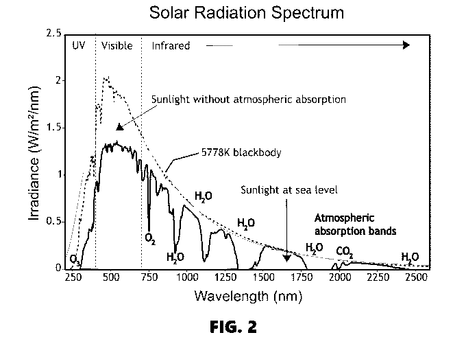
[0014] FIG. 2 is a graph showing the spectral distribution of solar energy.
[0015] FIG. 3 is a simplified schematic showing down conversion.
[0016] FIG. 4 shows power generated by polysilicon p-n junctions for incident
laser
CA 03157338 2022-04-07
WO 2021/076372
PCT/US2020/054596
- 4 -
light over a range of wavelengths.
[0017] FIG. 5 is a graph showing experimental observations, with power output
increase
as a result of increase in the photon density at a coherent wavelength.
[0018] FIG. 6 shows an exploded view of a solar panel according to an
embodiment of
the present disclosure.
[0019] FIG. 7 is a perspective view of an assembled solar panel.
[0020] FIG. 8 is an enlarged view showing a corner of an assembled solar
panel.
[0021] FIG. 9 is a graph that compares energy levels with and without optical
concentrator and bandpass filter.
[0022] FIG. 10 is a table showing comparative energy generation for different
arrangements, with and without optical concentrator and bandpass filter.
[0023] FIG. 11 is a flow diagram that shows a sequence for light handling that
provides
down-conversion for PV applications.
[0024] FIG. 12A is a graph that shows improved spectral response for a light-
propagating
material according to an embodiment of the present disclosure.
[0025] FIG. 12B is a graph that shows improved spectral response for a coated
light-
propagating material compared against pane glass transmission according to an
embodiment of the present disclosure.
[0026] FIG. 12C is a graph that shows spectral irradiance for incident light
and for light
that has been spectrally shifted by propagation through the coating of the
present
disclosure.
[0027] FIG. 12D is a graph that shows spectral irradiance vs. energy in eV
using different
coatings for spectral conversion.
[0028] FIG. 12E is a corresponding graph showing the change in relative photo
flux,
measured as number of photons per second per unit area.
[0029] FIG. 13 is a schematic side view showing a multi-layered coating for
down-
conversion of light energy.
CA 03157338 2022-04-07
WO 2021/076372
PCT/US2020/054596
-5-
100301 FIG. 14 is a side view schematic diagram that shows the layered
arrangement for
Bragg reflection used in a down-conversion coating.
[0031] FIG. 15 is a cross-sectional, partially exploded view that shows the
layered
arrangement used for a transparent down-conversion (DC) film or coating that
is formed
according to an embodiment of the present disclosure.
[0032] FIG. 16 shows a sequence for additive fabrication and forming in situ
nanoparticles within the coating.
[0033] FIG. 17 is a chart showing exemplary data for various coatings used for
spectral
conversion, according to an embodiment of the present disclosure.
DESCRIPTION OF EMBODIMENTS
[0034] Figures shown and described herein illustrate key principles of
operation and
fabrication for an optical apparatus according to various embodiments and are
not drawn
with intent to show actual size or scale. Some visual exaggeration may be
necessary in
order to emphasize basic structural relationships or principles of operation.
[0035] In the context of the present disclosure, terms "top" and "bottom" or
"above" and
"below" are relative and do not indicate any necessary orientation of a
component or
surface, but are used simply to refer to and distinguish opposite surfaces or
different light
paths within a component or block of material. Similarly, terms "horizontal"
and
"vertical" may be used relative to the figures, to describe the relative
orthogonal
relationship of components or light in different planes, for example, but do
not indicate
any required orientation of components with respect to true horizontal and
vertical
orientation.
[0036] Where they are used, the terms "first", "second", "third", and so on,
do not
necessarily denote any ordinal or priority relation, but are used for more
clearly
distinguishing one element or time interval from another. For example, there
are no fixed
"first" or "second" elements in what is taught herein; these descriptors are
merely used to
clearly distinguish one element from another similar element in the context of
the present
disclosure.
CA 03157338 2022-04-07
WO 2021/076372
PCT/US2020/054596
-6-
100371 In the context of the present disclosure, the term "film" can be used
to mean a
coating that is applied to a substrate as one or more thin layers, such as a
thin-film optical
coating formed from successively formed layers of materials treated to have
different
indices of refraction. A film can also be a sheet of a light-propagating
substrate formed
of one or more layers of optical materials and used in standalone fashion or
optically
coupled to another optical component, such as using an adhesive.
[0038] As used herein, the term "energizable" relates to a device or set of
components
that perform an indicated function upon receiving power and, optionally, upon
receiving
an enabling signal. A "light-propagating" material transmits or conveys the
bulk of the
light, at least more than 50%, received by the material. The range of interest
for light
propagation for PV conversion is generally between about 200nm and 2200nm.
[0039] The term "nanoparticle" generally refers to particles that have an
intermediate size
between individual atoms and macroscopic bulk solids, with an average diameter
between about 1 nm to 100 nm. Nanoparticle size for a material is typically on
the order
of the Bohr exciton radius, or the de Broglie wavelength of the material,
which may
allow individual nanoparticles to trap individual or discrete numbers of
charge carriers,
either electrons or holes, or excitons, within the particle. The spatial
confinement of
electrons (or holes) by nanoparticles is believed to alter the physical,
optical, electronic,
catalytic, optoelectronic and magnetic properties of the material.
[0040] Energy output of a PV device or system is proportional to the level of
absorption
of light photons of the proper energy bands. Improved absorption of energy-
generating
wavelengths can increase the efficiency of solar energy generation by an
appreciable
amount, resulting in lowered energy costs, with related advantages for
retrofit and rebuild
of earlier PV equipment now being used.
Solar Cell Function and Efficiencies
[0041] In order to better understand the nature and scope of solutions
provided by the
present disclosure, it is instructive to review the basic operation of typical
solar cells in a
PV device. A typical solar cell is a silicon p-n junction diode having a
depletion region.
In the absence of light, the cell behaves in similar fashion to a diode. When
light is
incident on the cell, the photons are absorbed by the silicon. This added
energy excites
CA 03157338 2022-04-07
WO 2021/076372
PCT/US2020/054596
- 7 -
silicon electrons, causing transition from the valence band to the conduction
band,
wherein the electrons are free to move. These excited electrons are called
"free carriers".
The electron transition creates a corresponding vacancy called a "hole". A
potential is
created across the depletion region as a result of recombination to form
neutral atoms there.
Metal contacts connected to the p and n regions give these electrons a flow
path, an
external circuit. The electrons can move according to this potential and
recombine with
the holes. This motion of electrons gives rise to an electric current, so that
the silicon cell
acts as a battery.
[0042] Among inherent limitations of existing PV cells are thermodynamic
constraints,
including Shockley-Queisser (S-Q) limits. From a thermodynamic perspective, it
can be
assumed that both the sun and solar cell are "black bodies" with full solar
energy incident
on the cell surface at a normal angle. Carnot work is assumed to be extracted
from the
cell by a heat engine. For the sun's temperature at 5760k and ambient
temperature of
300k, a maximum of 85% efficiency can be obtained at cell temperature of
2470k. At this
limit, all photons are considered to be absorbed; there is no thermal
dissipation and
maximum work is extracted from each photon.
[0043] The S-Q limit models the semiconductor cell as one material with a
single p-n
junction. It is assumed that all incident photons having energy higher than
the band gap
produce one electron-hole pair, per photon. All excess energy of the photon is
converted
to heat. The S-Q limit is based on the assumption that one sun of
unconcentrated solar
radiation is incident on a PV cell. The incident photon flux density is very
low and can
be increased up to about 500X using inexpensive optics.
[0044] For a semiconductor electron to move into an external load circuit, its
energy
level must be increased from its normal valence level to its higher energy
conduction level.
The amount of energy needed for a boost to the higher level is called the
"band gap"
energy. All photons having energy higher than the band gap energy can produce
a carrier
electron which produces electrical current. However, only the energy amount
equal to
band gap energy is used to excite the electron, the rest of the excess is
converted to heat.
Heating of the cell increases the dark current and decreases the overall
output of the cell.
Therefore, if the photons are close to the band-gap of the p-n junction of a
photovoltaic
CA 03157338 2022-04-07
WO 2021/076372
PCT/US2020/054596
- 8 -
solar cell, most of the photons get absorbed and the rest should be reflected
as they do not
contribute to the generation of electron-hole pair but heat the solar cell,
causing increase in
the dark-current.
[0045] Concentrated photovoltaics (CPVs) face the problem of efficiency
decrease
caused by the increase in the temperature of p-n junction, which leads to
higher dark
current, causing recombination of electrons and holes and reducing the charge
in the
conduction band.
[0046] In the proposed embodiment for photonic solar conversion, only photons
close to
the energy of band-gap of the irradiated p-n junction are allowed to reach
solar cells,
using an optical coating. Once the photons not absorbed at the band-gap of p-n
junction
(that is, photons that would otherwise cause heating of solar cells) are
eliminated using an
optical coating, the concentrated solar radiation can then linearly increase
power
generation with a corresponding increase in photon density.
[0047] The use of optical coatings for improving the energy output of PV cells
is
described, for example, in the following disclosures:
US Patent Application Publication No. 2008/0171191 Al by Gadomsky describes
the use of nano-structured antireflective optical coatings. However, existing
embodiments of photonic solar conversion use nano-optical coatings only as
band-pass filters.
US Patent Application Publication No. 2009/0084963 Al by Kost describes
apparatus and method for enhanced down conversion of photons with numerous
layers to trap photons but does not use a nano-optical coating or optical
concentrator.
WO Patent Application Publication No. 2015/138990 Al by Songo Jin et.al
describes solar energy absorbent coatings and methods of fabrication for
coatings
that absorb the solar spectrum over one wavelength region and reflect solar
energy over another portion of the spectrum. Power output, however, is
disappointing.
US Patent Application Publication No. 2006/0169971 Al by Cho et al. describes
CA 03157338 2022-04-07
WO 2021/076372
PCT/US2020/054596
- 9 -
an energy conversion film and quantum dot film that helps convert high energy
solar radiation to lower energy solar radiation using various quantum dot
sizes to
enhance solar energy conversion.
[0048] Various optical geometries for higher concentration of solar radiation
in
photovoltaic cells nave been proposed, but fail to sustain higher
efficiencies. In large
part, this shortcoming is due to increased temperature of the solar cells
under
concentrated solar radiation. In an embodiment of the present disclosure,
heating of the
solar cell is greatly reduced or eliminated due to an optical coating that
allows only
photons with energy close to the band-gap to be incident on the solar cells,
eliminating
most of the photons of higher energy that cause heating.
[0049] Significant industry research to-date has focused on improving the
efficiency of
silicon-based solar cells while increasing efficiency and reducing costs.
Little attention,
however, has been paid to the conditioning of the solar spectrum falling on
the PN
junction, which is the basis for electric power generation. In the proposed
innovation, the
focus is on the photons that reach the band-gap of the solar cells for maximum
absorption. By proper selection and distribution of light energy, the light
photons can be
conditioned to match the band gap of photovoltaic solar cells. This approach
proves to be
more promising than creating multi-junction solar cells, an approach that can
become
cost-prohibitive due to expensive band-gap engineering, e.g. tandem solar
cells.
[0050] FIG. 1 shows efficiency limitations vs. semiconductor band gap for
black body
conditions, with the S-Q (Shockley-Queisser) limit set for one electron-hole
pair per
photon for a number of types of solar cell materials. Excess photons are lost
to heat and
other effects. It has been found that about 47% of the incident energy is lost
as heat; 18%
of the energy is not converted and passes through the solar cell; 2% of the
energy is lost
in recombination effects. At best, the remaining 33% can be converted into
electricity.
The theoretical S-Q limit of a Silicon solar cell is thus 33%. Not considered
in the above
efficiency calculations are losses due to optical arrangements and
manufacturing defects.
[0051] Although some success has been shown using lanthanide elements and
quantum
dots, however, these materials are still fairly expensive and not acceptable
for broad
CA 03157338 2022-04-07
WO 2021/076372
PCT/US2020/054596
- 10 -
commercial use without significant environmental concerns. In response to the
need for
improved materials and results, the Applicant has found that a particular
arrangement that
combines nano-particles suitably structured and embedded in metal oxides can
achieve a
band-pass of 700 to 1100 nm and a low percentage of the down-shifting of the
solar
photons of 300 nm to 600 nm wavelength towards 800 nm to 900 nm low energy
photons. Transmittance and reflectance spectra for the experimental coating
has been
validated by independent testing. Outdoor testing indicates a gain of
efficiency for a 72-
cell full size panel, with overall improvement averaging from 15% to 22% in
solar panel
efficiency based on outdoor field trials.
[0052] According to an embodiment of the present disclosure, a photonic solar
conversion (PSC) process using an engineered nano-optical coating, as
described in more
detail subsequently, can down-convert high energy photons, having wavelengths
that
include ultraviolet (UV) wavelengths and a portion of visible light, to lower-
energy light
that is more closely tuned to the bandgap of c-Si cells. Down-conversion of
this type,
conditioning the light energy to more suitable levels for energy conversion,
is capable of
increasing the external quantum efficiency (EQE) of the photonic cells. A
coating formed
using down-conversion according to the Applicant's process can improve
efficiency of a
conventional, lower-cost solar panel by from 15% to 22%. In a broader aspect,
embodiments of the present disclosure can be used to provide wavelength
shifting of
incident light, including down-conversion, up-conversion, and bandgap
narrowing, for
example.
[0053] As is shown in the graph of the solar radiation spectrum in FIG. 2,
solar energy
has wavelengths ranging from about 300 to 2400 nm. The wavelengths that are
most
useful for solar energy PV conversion, using a bandgap at 1064 nm, lie in the
range
between about 400-1200 nm.
[0054] FIG. 3 shows, in simplified schematic form, the mechanism of spectral
down-
conversion, in which a high energy photon is converted to two lower energy
photons.
Conventional solutions for providing spectral conversion of this type in a
light-
propagating material rely heavily on lanthanide materials.
[0055] As one conventional practice, management of the solar spectrum for
conditioning
CA 03157338 2022-04-07
WO 2021/076372
PCT/US2020/054596
- 11 -
light and performing a measure of down-conversion using a photoluminescent
down-
conversion layer (PDL) with quantum dots and lanthanide ions is known. In
principle, as
is shown schematically in the simplified diagram of FIG. 3, down-conversion
takes place
because of the resonant transfer of one high energy photon to generate two or
more lower
energy photons, causing a gain of more than 100% in external quantum
efficiency (EQE).
[0056] For example, in a lanthanide ion layer which has praseodymium Pr3+ in
yttrium
fluoride YF3 host, a photon with high energy at 185 nm wavelength (approx.
6700 meV)
is first absorbed in the Lanthanide ion, then down-converted into two low
energy photons
of 408 nm and 620 nm (approx. 3040 - 2000 meV). The process is achieved in two
steps;
initially:
'So 4 3P1 at 408 nm;
then, the second conversion 3P1 4 3F2 at 620 nm.
[0057] The process of down-shifting high energy photons to numerous low energy
photons increases the probability that more than one electron will be
generated per
.. photon, thus increasing external quantum efficiency.
[0058] The uses and advantages of lanthanide elements, used in conventional
approaches
for energy down-conversion, are well-understood. The availability of electrons
in various
states that is characteristic of the lanthanides makes these substances
readily usable for
down-conversion applications. Other elements, meanwhile, do not enjoy this
inherent
.. advantage and would not be considered as likely candidate materials for
fabricating a
down-conversion article.
[0059] Lanthanide materials, however, present a number of problems in cost,
availability,
handling, and introduce a number of environmental concerns. Lanthanides also
show
considerable losses that constrain how much improvement can be obtained.
Photonic Solar Conversion
[0060] The Applicant's approach for improved efficiency of photovoltaics and
for other
applications in which spectral conditioning has value does not depend on
lanthanides or
phosphor-based light generation in order to shift the wavelength of light for
improved
efficiency in solar energy conversion. Instead, the Applicant has identified a
novel
CA 03157338 2022-04-07
WO 2021/076372
PCT/US2020/054596
- 12 -
sequence for light handling and energy conversion, along with a corresponding
layered
structure that can be engineered to provide the down-conversion that is most
useful for
photovoltaic and other applications. The Applicant's technique applies quantum
matching to the problem of wavelength shifting, forming a multilayered
structure that
takes advantage of both properties of Bragg reflection and efficiencies of
surface
enhanced Raman scattering.
[0061] Significantly, embodiments of the present disclosure can be used to
improve the
performance of solar panels that have already been installed. The Applicant
combines a
number of innovations in order to boost the power output of existing solar
panels,
including the following:
(i) Photon spectral conditioning. Conversion of solar radiation to coherent
light
energy at wavelengths close to the band-gap energy of the PV cell.
(ii) Nano-optical coating that acts as a band-pass filter and spectral
converter,
transmitting photons with energy levels (wavelengths) close to the band-gap
energy of the PV cell. According to an embodiment, a spectral converter
created
by the application of a group of metal oxide coatings is used to convert
radiation
from incident sunlight into a band pass of 100 nm around the optimum
wavelength close to 800 nm peak. Once the filter/spectral converter layer is
applied above the photovoltaic panel, a concentrator is used to increase the
intensity of solar radiation to 5x to 15x suns per unit area, increasing the
density
of incoming photons having a near optimum wavelength.
(iii) Increased photon density using at least one method of concentration,
such as
a concentrator focused on the PV cells. According to an embodiment, a
honeycomb of Fresnel lenses coated with the band-pass filter for optimum
wavelength is designed to achieve a 5x increase in the power output of the
solar
cell.
[0062] The target wavelengths for optimizing performance can be determined by
measuring the frequency response of given semiconductor solar cells with
variable
wavelength solid-state lasers. Laser output can be varied over a range, such
as increased
from 600 nm to 1100 nm, while measuring the output and efficiency at
incremental points
CA 03157338 2022-04-07
WO 2021/076372
PCT/US2020/054596
- 13 -
over the range. Response curves can be plotted accordingly.
[0063] By way of example, the graph of FIG. 4 shows power generated by
polysilicon p-
n junctions for incident laser light over a range of wavelengths. An optimum
value 400 is
at the peak output near 800 nm.
[0064] The graph of FIG. 5 shows experimental observations, with current
output
increase as a result of increase in the photon density at a coherent
wavelength. As shown
in FIG. 5, the increase in intensity of the coherent photon at the optimum
wavelength
laser beam incident on solar cell linearly increases the power generation.
[0065] The optical filter provided to direct light of the optimum wavelength
for the p-n
junction is used to block all other photons not useful for generation of
electrical energy in
the PV panel.
[0066] As shown in FIG. 5, the x-axis represents power input of the solid-
state laser with
photons with desired wavelengths irradiating the target p-n junction as Pin
power input.
The y-axis represents the maximum power output Pmax. The power output
increases
linearly with the increase in the power input. This indicates that the photons
close to
band-gap energy (matching energy) of the solar cell correspondingly increase
the
efficiency of photonic conversion to electricity. With power generation
increase linear
with photon intensity increase, photon conversion to suitable power levels.
[0067] Embodiments of the present disclosure increase power generation using a
combination of an optical concentrator and a spectral conversion optical
coating on a PV
panel substrate.
Solar panel arrangement
[0068] FIG. 6 shows an exploded view of a solar panel 600 formed according to
an
embodiment of the present disclosure. A layer of light concentrators 620 has
an array of
lens elements 622, such as an array of adjacent Fresnel lenses, for
concentrating light and
directing the concentrated light along light paths toward PV cells 612 arrayed
on a PV
array 610. A band pass filter/spectral conditioner 630 is disposed in position
in the light
path for conditioning the light that is conveyed between the light
concentrator and PV
arrays; the spectral conditioner 630 can be formed on or within a layer of
glass or other
CA 03157338 2022-04-07
WO 2021/076372
PCT/US2020/054596
- 14 -
optically transparent material having an optical coating. According to an
alternate
embodiment, the relative positions of the array 620 of light concentrators and
spectral
conditioner 630 can be reversed from that shown in FIG. 6, so that filtering
and spectral
conversion of the incident sunlight precedes concentration of the light in the
light path.
[0069] FIG. 7 shows solar panel 600 as assembled, according to an embodiment,
using
various types of clamps, brackets, or other fasteners 640 to hold array 610,
filter/spectral
conditioner 630, and concentrators 620 together in place, as a single unit.
According to
an embodiment of the present disclosure, distance between adjacent parallel
planes that
correspond to facing surfaces of the layered components is less than 20mm.
This
distance can be varied to suit the particular arrangement of optical
concentrators, for
example, or for improved performance of PV or light-conditioning components.
[0070] According to an embodiment of the present disclosure, the spacing
between
components 610, 620, and 630 can be adjustable.
[0071] FIG. 8 is a close-up view that shows a corner portion of solar panel
600 as
assembled.
Retrofit applications
[0072] For retrofit to existing solar panels having an array of PV devices, an
embodiment
of the present disclosure provides a suitable layer of light concentrators 620
and band
pass filter/spectral conditioner 630. Using a modular approach, the layer of
light
.. concentrators 620 and band pass filter/spectral conditioner 630 can be
designed, scaled,
and framed to suit the dimensions and the array geometry of the solar panel.
Light concentrators 620
[0073] To increase the number of photons passing through the nano-optical
coating or
enabled photonic bandpass filter layer, a host layer of optical concentrators,
such as an
array of Fresnel lens concentrators (having a honey-comb arrangement) can be
layered on
top of the photonic band pass filter. A device using a combination of low
concentration
optics (3X- 5X) with a band pass filter and coherence enhancement nano
coating, can
provide significant increase in energy generation from conventional
photovoltaic panels.
[0074] Planar light concentrator arrays are most advantageous for compact
packaging.
CA 03157338 2022-04-07
WO 2021/076372
PCT/US2020/054596
- 15 -
Various types of light concentrators can be used, in addition to Fresnel lens
elements. For
example, planar light concentrators can include holographic lens arrays and
GRIN
(gradient index) lens arrays, for example.
[0075] The light concentrators 620 and PV cells are aligned and arranged to
optimize the
energy collection that is provided for photovoltaic conversion. The spectral
conditioner
630 can be provided in array form or as a continuous sheet or coating, for
example.
Light-handling for band-pass filter/spectral conditioner 630
[0076] The optics industry has used coatings of various types, applied onto a
transparent
medium, for selective transmission and reflection of the solar radiation.
Chemical vapor
deposition (CVD) and physical vapor depositions (PVD) are mature techniques
that have
been adapted to form band-pass filters for restricting the wavelengths of
light passing
through the transparent medium. The Applicant has developed a proprietary
nanoparticle-based optical coating that aligns the wavelength distribution of
solar
radiated photons to more closely correspond to the band gap of mono crystal
silicon solar
cells while enhancing the coherence of the photons using the band pass
filter/spectral
converter 630 formed on the substrate, such as provided using a coating.
[0077] To accomplish photonic solar conversion, a thin film optical filter
technology has
been configured to restrict transmission of solar radiation within a given
band-pass.
Photons received by the p-njunction solar cells (e.g. by the Si solar cells)
have an
electromagnetic radiation energy level. The spectral response to absorption of
the solar
cells increases linearly as the wavelength of the incident light comes closer
to the bandgap.
Hence, two effects are desirable: 1) to constrain the wavelengths so that they
are close to
the bandgap; and 2) to create an abundance of photons having wavelengths that
are
sufficiently close to the bandgap of the p-n junction in order to optimize
absorption.
[0078] Solar radiation has wide range of wavelengths as shown in FIG. 2,
ranging from
300 nm to 2400 nm. The region of interests for solar energy photovoltaic
conversion for
Si solar cells with band-gap at 1064 nm is in the region between about 400 nm
(visible)
and 1200 nm (infrared). Solar radiation above the band gap passes through the
band gap
and is not useful for photovoltaic conversion.
CA 03157338 2022-04-07
WO 2021/076372
PCT/US2020/054596
- 16 -
[0079] In order to condition the solar radiation for increased efficiency, the
Applicant has
developed a band pass filter/light conditioner 630 as a thin film optical
filter, formed
using chemical vapor deposition or other suitable deposition method, that
conditions the
solar radiation to shift toward wavelengths from 800 nm to 1100 nm. This band
pass
filter is formed using a combination of metal oxides e.g. SiO2 and TiO2. These
oxides
are used to generate a proprietary mix of nano-particles. For example,
divalent
manganese and trivalent chromium fluoresce at wavelengths close to the p-n
junction
bandgap of 1064 nm. This proprietary thin coating provides the necessary
conditioning of
photons for more suitable wavelengths in this range. A filter layer formed in
this manner
can be applied onto a glass substrate, in the path of light to the array of
photovoltaic cells.
An optical concentrator can then be used to increase the concentration of
photon density
to up to 10 to 100 suns per unit area.
[0080] The graph of FIG. 9 shows a comparison of energy levels obtained using
three
different component arrangements: bare-cell PV output 910, PV generation with
an
added lens or other optical concentrator as output 920, and PSC generation 930
using an
added band pass filter as output, according to an embodiment of the present
disclosure.
The table in FIG. 10 shows representative energy values for the PV, PVC, and
PSC cases
in measurements (Watt-hrs.) taken over a four-day period.
Band pass filter/light conditioner configuration
[0081] The flow diagram of FIG. 11 shows a sequence for light handling that
provides
down-conversion or other types of spectral shifting as executed by band pass
filter/spectral conditioner 630. According to an exemplary embodiment, this
sequence
can be used for shifting a portion of the higher energy UV and visible light
in the
received sunlight radiation to the lower energy bandgap range of a
conventional silicon
PV cell, 1064 nm. The sequence achieved by the Applicant's coating is as
follows:
(i) Step S200: Receive incident light energy. For incident sunlight, for
example, most of the irradiance is within the visible region, roughly
between about 450-700 nm.
(ii) Step S210: Perform spectral shift and selection using distributed
Bragg reflection (DBR) with quantum confinement.
CA 03157338 2022-04-07
WO 2021/076372
PCT/US2020/054596
- 17 -
(iii) Step S220: Perform a further spectral shift using surface-enhanced
Raman scattering (SERS).
(iv) Step S230: Transmit the light for energy harvesting; this includes the
spectrally shifted light, such as at a PV converter 20.
.. [0082] As a result of photovoltaic action, electrical current is generated
following step
S230. The generated electrical current can be stored, such as in a battery or
other storage
cell, or can be directly used for obtaining electrical energy.
[0083] It should be noted that concentration of the light energy is not shown
in the
sequence of FIG. 11. In one embodiment, as described with reference to FIG. 6,
the light
.. energy received at step S200 has been concentrated at concentrator array
620. According
to an alternate embodiment, light concentration is performed following the
spectral shift,
that is, between steps S220 and S230 in the FIG. 11 sequence.
[0084] The graph of FIG. 12A compares the transmission spectra of an uncoated
optical
glass with the transmission spectra of the same glass material having a
coating formed
.. according to an embodiment of the present disclosure. As can be seen, the
transmission
efficiency is enhanced for higher wavelength light. This enhancement can be
beneficial
for PV applications. FIG. 12B shows improved spectral response for a coated
light-
propagating material used as spectral conditioner 630 compared against pane
glass
transmission according to an embodiment of the present disclosure.
.. [0085] The graph of FIG. 12C shows spectral irradiance for incident light
in air (dashed
line) and for light that has been spectrally shifted by propagation through
the coating of
conditioner 630 of the present disclosure (full line). Shading shows the
corresponding
shift in energy distribution and change in overall power density.
[0086] FIG. 12D is a graph that shows spectral irradiance vs. energy in eV
using different
.. coatings for spectral conversion (with data labeled PSC 3, 4, 5), relative
to the air mass
(AM1.5) standard.
[0087] FIG. 12E is a corresponding graph showing the change in relative photo
flux,
measured as number of photons per second per unit area, relative to energy in
eV.
[0088] The cross-section of FIG. 13 shows, in schematic form and not to scale,
the
CA 03157338 2022-04-07
WO 2021/076372
PCT/US2020/054596
- 18 -
structure of band pass filter/spectral conditioner 630. Component 630 has an
arrangement of layers that can be used to provide a coating 40 on a
transparent substrate
52, wherein coating 40 has the described spectral behavior for down-conversion
of light
energy in a PV application, with the light incident from above in the
orientation shown.
.. A cover 42 is formed from a light-propagating material, typically glass or
plastic. A
modified distributed Bragg reflector (DBR) section 44 is a multilayer
structure that
provides the first spectral shift with selection noted in the FIG. 2 sequence
by changing
the coherence length of a portion of the incident light. The spectrally
shifted light is then
directed to a surface-enhanced Raman scattering (SERS) layer 46, wherein
subsequent
spectral shifting takes place. The resulting light energy shifted toward the
bandgap
desired, such as bandgap of a PV device for example, can then be directed to a
PV
material or other substrate.
Structure and composition of Bragg reflector section 44
[0089] Embodiments of the present disclosure use principles of Bragg
reflection,
modified for quantum matching, as described following. It must be noted that
Bragg
reflection, of itself, does not cause a spectral shift, but is rather used for
selective
reflection of a narrow portion of the spectrum. In order to better understand
the
additional shifting mechanism that is formed within the Bragg reflector
structure, it is
useful to first review some basic principles of Bragg reflection. The
distributed Bragg
.. reflector arrangement can alternately be considered a 1-D photonic crystal,
formed as a
periodic arrangement of microstructures that collectively define particular
energy bands.
[0090] The schematic side view of FIG. 14 and exploded view of FIG. 15 show an
arrangement of multiple layers 60, 66 for Bragg reflector section 44 according
to an
embodiment. Bragg reflector section 44 is formed as a quarter-wave stack that
provides a
.. photonic crystal. A sequence of transparent layers, overlaid on one
another, has alternate
layers having alternating indices of refraction, with indices shown
respectively as nl, n2.
Four layers are shown in FIG. 1; additional layers could alternately be used
for forming a
Bragg reflector. According to an embodiment, 6-12 periods are used, each
period having
a pair of layers of alternate indices. The periodic variation in refractive
index can be
.. provided by layers having X /4 thickness, wherein, wavelength X is at a
suitable
CA 03157338 2022-04-07
WO 2021/076372
PCT/US2020/054596
- 19 -
wavelength for the particular application. According to an exemplary
embodiment of the
present disclosure, the target Bragg wavelength X is about 600nm.
[0091] Layer thickness, alternating slightly between values dl and d2 for the
different
materials that have respective indices n1 and n2, can provide Bragg reflection
at a Bragg
wavelength 4, with the alternating thickness values given by:
1 AB
d1 = ¨ ¨
4 ni
1 AB
d2 =
n2
With silicon (Si), layer thickness is typically in the 60 nm range.
[0092] The period A of the Bragg layer sequencing can be expressed:
AB [ 1
A = di + d2 = ¨ ¨ 1
2 2n1 2n2
or
1 AB r+ n2]
A= ¨ wherein 77 =
2n 2
Thus,
(= 1
)
n = 2 n1 n2
[0093] With a Bragg reflection wavelength:
AB = 2TAB
a propagation constant can be obtained:
27r if
igB = =
zt,B
[0094] For light at wavelength:
4: LP¨P-PB
[0095] For light in phase with the grating, the difference between indices n1
and n2 is
relatively small. At the Bragg wavelength, transmission loss can be
exceptionally low;
CA 03157338 2022-04-07
WO 2021/076372
PCT/US2020/054596
- 20 -
reflectivity at this wavelength can exceed 99.99%.
[0096] Other, more conventional proposed solutions for handling light to or
within
photovoltaic devices use Bragg reflectance to trap or otherwise contain the
incident light,
but lack the capability to provide a wavelength shift. Embodiments of the
present
disclosure address the problem of wavelength shifting using quantum matching
in
forming the distributed Bragg reflector structure. In a quantum-confined Bragg
grating,
the reflector arrangement maintains light energy at an antinode, for
enhancement of
optical gain by a factor of 2.
[0097] According to an embodiment, quantum confinement or quantum matching is
achieved using a distribution of silicon (Si) nanoparticles/nanocrystals
embedded within a
silicon oxide (5i02) substrate. Spaces between the distributed nanoparticles
form
vertical cavities within the 5i02 substrate ("vertical" extending in a
direction generally
orthogonal to the plane of layers and of the PV device surface). Resonance of
the light
signal within the cavities results in coherence of the light, at frequencies
(wavelengths)
that correspond to the overall distribution and vertical distance of these
cavities. Thus, in
quantum matching, the relative concentration and distribution of nanoparticles
within
each of one or more layers of the DBR structure has impact on both the index
of
refraction of the Si/5i02 layer and on the range of spectral shifting that is
obtained.
[0098] According to an embodiment of the present disclosure, two different
layers
alternate in the DBR coating 40 structure:
(i) layers 60 in the layered arrangement shown in FIG. 5 are formed of an
engineered material having a distribution of Si particles within an 5i02
substrate;
and
(ii) alternate layers 66 are formed of another transparent, conducting
material such
as indium-tin oxide (ITO). Alternative materials that can also be used include
various types of doped binary compounds, including aluminum-doped zinc oxide
(AZO), indium-doped cadmium oxide, and aluminum, gallium, or indium-doped
zinc oxide (AZO, GZO, or IZO), for example.
[0099] Materials used for providing substrate and nanoparticle components are
selected
CA 03157338 2022-04-07
WO 2021/076372
PCT/US2020/054596
-21 -
for suitability for forming vertical cavities having appropriate geometry for
the target
wavelengths.
Structure and composition of SERS layer 46
[00100] Referring back to the schematic diagram of FIG. 13, SERS layer 46
forms a
wavelength conversion engine that provides additional wavelength shift to the
incoming
light, following conveyance of the light and initial shifting of wavelength
through Bragg
reflector section 44.
[00101] Regarding the down-conversion of photons with scattering and Stokes
shift, it
has been shown that near resonant Raman scattering, given an ultraviolet (UV)
or visible
(VIS) excitation source such as 325 nm excitation source, gives rise to T2
(LO) peaks in
the infrared (IR) energy region. Thus, for example, the 325 nm source can
generate
peaks within a region of interest 600 nm to 1050 nm. The intensity of the
generated
T2(LO) peaks increases with ZnS nano-particle size from 6 nm to 30 nm.
[00102] In an embodiment, the surface enhanced Raman effect causes the UV and
VIS
.. in the range of 350 nm to 450 nm to excite T2(LO) peaks in the 600 nm to
1000 nm
region as a result of Raman shift (Stokes shift). This shift may be caused by
the change
in bandgap energy caused by the quantum confinement and free exciton emission
energy
created by surface plasmons. The ZnS metal nano-particles provide the
necessary
plasmonic energy for the Stokes shift and hence do not cause loss in the
energy of the
shifted photons emitted in the region of interest.
[00103] Raman scattering is a result of formation of a dipole cloud from
electrons of
the molecular materials. Spectral shifting and surface enhancement of the
Raman
scattered signals results from the distribution of conductive nanoparticles of
appropriate
materials, such as silver, gold, and zinc, for example, within the substrate
that forms
.. SERS layer 46. By appropriate selection of materials and their
distribution, the SERS
layer 46 can be configured to exhibit localized surface plasmon resonance
(LSPR) to
provide spectral shifting toward a suitable wavelength range. The term
"conductive" used
herein refers to having a relatively low volume resistivity, e.g., without
limitation, a
volume resistivity that is less than 1020hm-m at 20 C. Volume resistivity
relates to the
ability of a material to oppose the flow of electric current.
CA 03157338 2022-04-07
WO 2021/076372
PCT/US2020/054596
- 22 -
[00104] The SERS layer 46 provides localized surface plasmon resonance (LSPR)
to
provide spectral shifting to a suitable wavelength range.
[00105] Propagation of light through a medium with a sparse distribution of
embedded
nanocrystals can be approximated by the effective refractive index of a
homogeneous
medium, computed as:
= m [27rp
1_ +k3S(0)1
wherein:
m = refractive index of the light-conveying medium in which nanoparticles are
embedded;
k = ¨ wavenumber in the medium;
p = ¨v number of particles N divided by the volume V;
S(0) scattering amplitude in the forward direction;
[00106] The absorption coefficient, wherein the absorption medium has complex
refractive index is generally:
a = 2k in, in
for a thin layer with small, identical nanoparticles the absorption
coefficient is given by:
m47rp
a = ________
k 2
Re S(0) = Pincext
wherein cext is the extinction cross section of a single particle,
proportional to the real part
of the scattering amplitude Re S(0).
[00107] According to Beer's law, the attenuation of a collimated beam
propagating
through the effective medium over a distance h is obtained using:
1(h) = 1 (0) e -hmpcext
wherein I is the intensity.
CA 03157338 2022-04-07
WO 2021/076372
PCT/US2020/054596
- 23 -
[00108] Wavelength shifting occurs due to interaction between competing
processes,
as described in the article by van Dijk et al. entitled "Competition between
Extinction and
Enhancement in Surface-Enhanced Raman Spectroscopy" in Physical Chemistry
Letters,
American Chemical Society, 2013. pp. 1193-1196, incorporated herein by
reference.
SERS operates to cause extinction of the resonant signal at plasmon
frequencies for the
nanoparticles, with corresponding enhancement of the Raman scattered signal at
a
distance from the resonant wavelength. This counter-intuitive behavior, with
diminished
Raman signal when nanoparticles are excited at plasmon resonance, can be
adapted to
provide up-conversion of the incident light to longer wavelengths, which is
typically the
behavior desired for PV applications. Alternately, SERS can be used to effect
down-
conversion of the incident light to shorter wavelengths, as well as wavelength
band
matching.
[00109] Among factors that can be controlled in order to adjust the wavelength
and
intensity of the Raman scattered light energy are nanoparticle type, shape,
overall size,
and concentration/distribution. Design of spectral response with SERS
structures is
described, for example, in an article by A. Bouali, S. Haxha, F. Abdelmalek,
M. Dridi,
and H. Bouchriha entitled "Tuning of Plasmonic Nanoparticle and Surface
Enhanced
Wavelength Shifting of a Nanosystem Sensing Using 3-D-FDTD Method" in IEEE
Journal of Quantum Electronics Vol. 50, No. 8 (August 2014), pp. 651-657,
incorporated
herein by reference.
[00110] A plasmon resonant material scatters incident light over a frequency
spectrum
that is characteristic of the material's particle diameter, size, and
dielectric attributes of
the surrounding substrate. Resonantly scattered light for some materials can
increase the
wavelength, such as to provide a "red-shift", to incident light.
[00111] A feature of plasmon creation in a metallic particle is the generation
of
enhanced electric fields in the region near its surface. Interactions between
this electric
field and nearby materials can significantly alter both the scattering
characteristics of the
resonant particle and the nearby material. Surface Enhanced Raman Spectroscopy
(SERS) exploits the localized plasmon resonance in particle-coated films,
engineered to
enhance Raman scattering by a few orders of magnitude. Using this technique,
Raman
CA 03157338 2022-04-07
WO 2021/076372
PCT/US2020/054596
- 24 -
scattering from the materials of interest can be observed; the local field
generated by the
plasmon can be used to enhance the intensity of that scattering.
[00112] According to an embodiment of the present disclosure, SERS layer 46 is
formed of metallic nanoparticles formed of zinc oxide (ZnO) or other
transparent,
conductive metal, embedded within a transparent, conductive base material or
matrix.
According to an embodiment of the present disclosure, ITO is the conductive
base
material. A number of types of metallic nanoparticles can be used for
obtaining plasmon
response in SERS layer 46, depending on the amount of wavelength shifting that
is
required. Suitable metallic nanoparticles can include noble metals such as
gold and
silver, and metals with favorable qualities for low reactivity and high
reflection, including
cobalt, and chromium, for example. Various compounds such as zinc nitrate can
alternately be used. As is known to those skilled in the quantum electronics
arts, the
amount of spectral shift that is provided can be engineered into the material,
such as by
applying a suitably designed coating. The spectral shift that is achieved can
be, in part, a
factor of nanoparticle size and distribution and of the complex index of
refraction of the
base material or matrix.
[00113] It should be noted that the use of various types of nanoparticles and
control of
their relative sizes and distributions within the different layers of the film
or coating of
the present disclosure allows adjustment of light wavelengths that enables use
for up-
conversion, down-conversion, or wavelength band matching.
Fabrication of Down-Conversion Film
[00114] For solar energy conversion applications, for example, the Applicant
has
found that a down-conversion coating or film 40 can be formed using the
arrangement
described previously to provide suitable wavelength shifting that conditions
incident
sunlight to wavelengths that are more favorable for efficient conversion by PV
devices.
[00115] With respect to the layered arrangement shown in FIGs. 13-15,
fabrication
steps begin with cover 42, which can be a transparent glass or plastic
substrate, then form
the layers of the Bragg reflector section 44 onto cover 42, followed by
formation of
SERS layer 46.
CA 03157338 2022-04-07
WO 2021/076372
PCT/US2020/054596
- 25 -
[00116] Steps for forming coating 40 onto cover 42 as a base can use the
following
sequence:
[00117] (i) Form a first layer 66 using sputtering or other deposition
technique to
deposit 50 nm of ITO or other conductive, light-conveying material.
[00118] (ii) Sputter or otherwise deposit a thin layer of Si onto layer 66.
[00119] (iii) Use sintering or annealing to form nanocrystals from the
deposited Si
layer. According to an embodiment, sintering temperatures in the 600-800
degrees C
range form Si nanocrystals of suitable size and distribution for forming layer
60 with a
given index of refraction that differs from that of the ITO layer and having
desired
nanocrystal distribution for forming vertical cavities for Bragg reflection at
suitable
wavelengths.
[00120] (iv) Form an embedding layer by depositing ITO or other conductive,
light-
conveying material onto the nanocrystals formed.
[00121] (v) repeat steps (i) - (iv) two or more times to form Bragg reflector
section 44.
[00122] (vi) Form the SERS layer by applying a conductive, transparent base,
such as
ITO, and embedding or otherwise distributing ZnO onto the base.
[00123] (vii) Form nanoparticulate ZnO particles with suitable
distribution for
generating SERS.
[00124] There are a number of known methods for forming nano-optical coatings.
These methods include, but are not limited to, roll coating, spin coating,
physical vapor
deposition, chemical vapor deposition and magnetron plasma sputtering. Roll
coating
has disadvantage of using a filler formed of polymer binders and fillers that
degrade
when exposed to sunlight.
[00125] Magnetron plasma sputtering can be used for nano-optical coatings of
inorganic, long-lasting metal oxides, such as, TiO2, 5i02, MgF2, for example.
This
technique allows in-line processing, with the capability to sputter a large
number of glass
sheets within favorable cycle times. The magnetron plasma sputtering technique
builds
the nano-optical coating layer-by-layer, as an additive fabrication process.
CA 03157338 2022-04-07
WO 2021/076372
PCT/US2020/054596
- 26 -
[00126] The diagram of FIG. 16 shows a sequence for additive fabrication and
forming in situ nanoparticles within the coating. From left to right,
sputtering is used to
apply the material and related oxide to a substrate (at the sample position).
An annealing
process, under controlled conditions such as in a N2 / 02 atmosphere, is then
used to
condition the coating to its substrate. Temperatures for annealing are
typically in the 900-
1200 degree C range, without limitation. The resulting nanoparticles can be
tested and
used to provide the desired transmissive and reflective properties.
[00127] For nano-particle inclusion in the matrix of the transparent material,
such as
within Transparent Conducting Oxides (TCO), for good contact at the top and
bottom
surface of the single junction c-Si solar cells, thermal annealing can be
obtained. Thermal
annealing of the sputtered layer of metal oxide to create in-situ
nanocrystals, again using
an additive manufacturing process, allows improved control; applying the
annealing
temperature and pressure, using methods familiar to those skilled in the
materials art,
allows the precise control of size and density of the nanocrystal active
layer.
[00128] The additive manufacturing sequence described is suitable for in-
line, high
throughput processing. Quartz heaters can be incorporated within the
sputtering chamber.
The coating can include at least one layer of fluorescent nanoparticles.
[00129] According to an embodiment, there is a sequence of steps that combines
nano-
particles suitably structured and embedded in metal oxides to achieve a band-
pass of 700
to 1100 nm and a low percentage of the down-shifting of high-energy photons of
300 nm
to 600 nm wavelength towards 800 nm to 900 nm lower-energy photons, more
suitable
for PV and other applications. Transmittance and reflectance spectra for the
experimental
coating has been validated by independent testing. Outdoor testing, for
example, indicates
a gain of efficiency for a 72-cell full size solar panel, with overall
improvement averaging
from 15% to 22% in solar panel efficiency based on field trials.
[00130] The cross-sectional view of FIG.13 shows (not to scale) the layered
arrangement used for band pass filter/spectral conditioner 630 using layers
applied to a
glass substrate 52. According to an embodiment, the needed layers of material
can be
formed and provided as a film or coating. The provided film or coating can be
fabricated
in rolled or sheet form, then applied to a substrate surface using an optical
adhesive, such
CA 03157338 2022-04-07
WO 2021/076372
PCT/US2020/054596
- 27 -
as EVA (ethylene-vinyl acetate), for example.
[00131] According to an embodiment of the present disclosure, the substrate is
a low-
iron solar glass, such as solar glass products manufactured by Gujarat Borosil
Ltd.,
Gujarat, India.
[00132] Layers can be formed on the light-propagating substrate by any of a
number
of suitable methods, such as by physical or chemical vapor deposition.
Sintering and
annealing processes can be executed under high vacuum or in an oxygen-free
environment, for example.
[00133] According to an alternate embodiment of the present disclosure, a
layered film
as shown in FIG. 13 and described herein can be formed on a film substrate for
application to glass or other optical material or component. Alternately, the
layers that
form the filter can be formed directly onto a surface of a light-propagating
material or
photonic component for improved spectral efficiency and response.
[00134] Although described in an embodiment for down-conversion function, the
apparatus and methods of the present disclosure can alternately be applied,
with suitable
changes in material distribution and size, for up-conversion, as well as for
shifting of
light energy to a preferred wavelength range.
Preliminary Results with Mono-crystal Si Solar Cell
[00135] Preliminary experiments were carried out by the Applicant as proof of
concept
for a Photonic Solar Conversion process. Mono crystalline Si single solar
cells (152x152
mm) were subjected to three comparative conditions using a dynamic test
platform with
one-axis tracking of the sun. The three conditions tested were:
[00136] Bare PV cell (PV)
[00137] PV cell with Fresnel concentrator (PV-C)
[00138] Photonic Solar Conversion panel with PV cell with nano photonic filter
and
Fresnel concentrator (PSC-SP)
[00139] The preliminary result indicates that the power generation wattage for
the bare
PV is the lowest power generated. The same PV cell with optical concentrator
increases
CA 03157338 2022-04-07
WO 2021/076372
PCT/US2020/054596
- 28 -
power generation but, due to increased temperature, reduces the power
generation. The
highest power generation is obtained by the combination of photonic filter
with band-pass
of 700 nm to 1100 nm and concentrator as shown in FIG. 6 and the graph of FIG.
9. The
x-axis represents time of the observation, the y-axis represents the energy
generation in
Watt hours. The three conditions are graphed ¨ output 910 represents the bare
PV cell,
followed by output 920 representing an arrangement of the PV cell with an
optical
concentrator (PVC). The output 930 graph represents the PV cell with nano-
optical filter
and concentrator assembly.
[00140] Power generation for PV-C configuration is initially higher than the
PSC-SP
.. but, with time, flattens out and drops lower than the PSC-SP power
generation. The FIG.
10 compares the three configurations conducted over three days and, for longer
term data
measurement, over seven days.
[00141] FIG. 9 indicates gain by the PV-C and PSC-SP indicates that PSC-SP
panels
with photonic filter and concentrator is consistently higher than both PV and
PVC with
.. concentrator. The higher gains in energy generation can be attributed to
the conditioning
of photons with wavelengths close to the Si p-n junction bandgap, and
abundance of the
wavelengths close to optimum absorption wavelength of 850 nm. The percentage
gain for
the PVC/PV averages nearly 100% but decreases significantly with the increase
in
temperatures of the solar cells. The percentage gain for single PV cell with
PSC-SP
configuration is close to 200% on average and remains consistent, as the solar
cell
temperature does not increase, even with 5x concentration. This preliminary
data on three
configurations shows the efficacy of the proposed apparatus.
[00142] The chart of FIG. 17 shows exemplary data for various coatings used
for
spectral conversion, according to an embodiment of the present disclosure.
[00143] According to an embodiment of the present disclosure, an optical
coating has
a set of layers formed to reflect a predetermined range of wavelengths, the
set of layers
including two or more pairs of alternating first and second layers, the first
layers having a
first refractive index, ni, and the second layers having a second refractive
index, nz,
greater than the first refractive index ni, wherein the second layers each
include a first
distribution of nanoparticles of a first material, wherein the layers exhibit
a spectral
CA 03157338 2022-04-07
WO 2021/076372
PCT/US2020/054596
- 29 -
characteristic that shifts a portion of the incident light wavelengths to a
first range of
wavelengths and that directs light of the first range of wavelengths to a
surface-enhanced
Raman scattering layer. The surface-enhanced Raman scattering layer is
configured with
a second distribution of conductive nanoparticles of a second material to
further shift the
light of the first range of wavelengths to a second range of wavelengths
different from the
first range, according to the second distribution of nanoparticles in the
Raman scattering
layer. The spectral characteristic of the layers can be provided by reflective
cavities
formed within the first distribution of nanoparticles. The first material can
be silicon; the
second material can be a conductive metal. The coating can be formed as a
film.
[00144] An optical coating in accordance with an embodiment of the present
disclosure can have a distributed Bragg reflector section that is configured
to reflect a
target wavelength; and a surface-enhanced Raman scattering section that is
adjacent to
the DBR section and is configured to accept light of the target wavelength
from the DBR
section and generate light that is spectrally shifted from the received light.
[00145] According to an embodiment of the present disclosure, there is
provided an
apparatus for solar energy power conversion comprising: a planar array of
light
concentrators distributed in a pattern, for example, a honeycomb pattern or a
row-column
pattern; a planar array of PV cells distributed in light-path alignment with
the light
concentrators; and a spectral converter that extends between the planar array
of light
concentrators and the planar array of PV cells, wherein the spectral converter
is
configured to convert incident light of a first spectral distribution from the
array of light
concentrators to outgoing light of a second spectral distribution for the
array of PV cells.
[00146] The spectral converter can comprise a coated glass sheet. The coating
can be
formed of two or more layers of metal oxide. Light concentrators can be
Fresnel lenses.
The second spectral distribution can have increased light energy over a
spectral range
associated with a band gap of the PV cells. There can be an encapsulating
casing.
[00147] According to an embodiment of the present disclosure, an apparatus for
retrofit to a photovoltaic cell array for solar power conversion comprises: a
planar array
of light concentrators distributed in a pattern corresponding to the
photovoltaic cell array;
a spectral converter that extends between the planar array of light
concentrators and the
CA 03157338 2022-04-07
WO 2021/076372
PCT/US2020/054596
- 30 -
PV cell array, wherein the spectral converter is configured to convert
incident light of a
first spectral distribution from the array of light concentrators to outgoing
light of a
second spectral distribution for the PV cells. The Fresnel lens can be made
from any
transparent polycarbonate material or group of polycarbonate materials, for
example.
[00148] According to an embodiment, the optical coating can generate photon
energy
at multiple wavelengths. A glass substrate may or may not have an anti-
reflection
coating.
[00149] The invention has been described in detail, and may have been
described with
particular reference to a suitable or presently preferred embodiment, but it
will be
understood that variations and modifications can be effected within the spirit
and scope of
the invention. The presently disclosed embodiments are therefore considered in
all
respects to be illustrative and not restrictive. The scope of the invention is
indicated by
the appended claims, and all changes that come within the meaning and range of
equivalents thereof are intended to be embraced therein.