Note: Descriptions are shown in the official language in which they were submitted.
WO 2021/092233
PCT/US2020/059192
SYSTEM AND METHOD USING MULTILAYER QUBIT LATTICE ARRAYS FOR
QUANTUM COMPUTING
BACKGROUND
Field
[0001] This application is generally directed
to quantum computing (QC), and
more particularly to quantum computer architectures employing lattice array
structures of more
than one dimension.
Description of the Related Art
[0002] Technology paths toward scalable
quantum computing have been
diverse. Demonstrated performance in the various figures of merit vary widely
according to
the type of physical quantum bit (also referred to as a "qubit") employed by
each
approach. Approaches based on either trapped ions or on superconducting qubits
have
consistently led the field through more than two decades.
SUMMARY
[0003] Certain implementations disclosed
herein provide a quantum computer
architecture employing a lattice array structure of more than one dimension
for implementing
and interconnecting quantum gates in which more than two qubits can be
simultaneously
entangled. Certain implementations disclosed herein provide quantum
microprocessor
configuration and gate array design platforms for quantum processing chips,
analogous to field
programmable gate arrays (FPGAs) which can advantageously provide a degree of
reconfigurability. Certain implementations disclosed herein provide quantum
microprocessor
configuration and gate array design platforms for quantum processing chips,
analogous to
application specific integrated circuits (ASICs) which can advantageously be
optimized for a
specified application and can advantageously provide custom design
flexibility.
[0004] Certain implementations disclosed
herein comprise lattice configurations
comprising multiple fully-connected qubits arranged as arrays of three-
dimensional (3-D)
lattice structures (e.g., cells), with simultaneous multi-qubit gate
operations enabled by qubits
arrayed in geometric layouts. For example, certain implementations can be
configured as
multiple two-dimensional (2-D) (e.g., planar) qubit arrays (e.g., layers) that
are substantially
parallel to one another and that form arrays of three-dimensional (3-D) cells.
For another
-1-
CA 03157734 2022-5-9
WO 2021/092233
PCT/US2020/059192
example, certain other implementations can be configured as multiple one-
dimensional (1-D)
(e.g., linear) qubit arrays (e.g., rows and columns; lattices; chains) that
are substantially parallel
to one another. In both of these examples, the arrays of cells can be
analogized to or referred
to as 3-D crystal structures. While various implementations are described
herein as utilizing
trapped ion qubits (e.g., in microchip structures) to illustrate the nature of
quantum interactions
to be utilized (e.g., optimized), other implementations can use one or more
alternative qubit
technologies.
[0005] Certain implementations disclosed
herein provide a quantum computing
(QC) system comprising a plurality of qubits arranged substantially in a
plurality of
substantially planar regions (e.g., planes; layers) that are substantially
parallel to one another,
at least some of the substantially planar regions comprising two or more
qubits and one or
more qubits of each substantially planar region configured to interact with
one or more qubits
of at least one neighboring substantially planar region. For example, the QC
system can
comprise a first substrate and a second substrate, the first substrate and the
second substrate
substantially parallel to one another, and the QC system can further comprise
a multiple-qubit
gate array comprising the plurality of qubits arranged as a plurality of
multiple-qubit gates
positioned in a region between the first substrate and the second substrate.
The qubits of the
multiple-qubit gate array can comprise surface electrode traps configured to
contain ions (e.g.,
charged atoms; charged molecules) at or near a surface of at least one of the
first and second
substrates, and can be arranged substantially in a plurality of substantially
planar regions (e.g.,
planes; layers; levels), with at least some of the qubits of at least one
substantially planar region
configured to interact (e.g., to be quantum-mechanically entangled) with at
least some of the
qubits of at least one other (e.g., neighboring) substantially planar region.
[0006] Certain implementations disclosed
herein provide a quantum computing
(QC) system comprising a plurality of qubits arranged substantially in a
plurality of linear
arrays that are substantially parallel to one another, at least some of the
linear arrays comprising
two or more qubits and one or more qubits of each linear array configured to
interact with one
or more qubits of at least one neighboring linear array. For example, the QC
system can
comprise a multiple-qubit gate array comprising the plurality of qubits
arranged as a plurality
of multiple-qubit gates positioned in a region between two or more substrates.
The qubits of
the multiple-qubit gate array can comprise surface electrode traps configured
to contain ions
-2-
CA 03157734 2022-5-9
WO 2021/092233
PCT/US2020/059192
(e.g., charged atoms; charged molecules) at or near a surface of at least one
of the substrates,
and can be arranged substantially in a plurality of linear arrays, with at
least some of the qubits
of at least one linear array configured to interact (e.g., to be quantum-
mechanically entangled)
with at least some of the qubits of at least one other (e.g., neighboring)
linear array.
BRIEF DESCRIPTION OF THE DRAWINGS
[0007] The accompanying drawings, which are
incorporated in and constitute a
part of this specification, illustrate one or more implementations described
herein and, together
with the description, explain these implementations.
[0008] FIGs. 1A-1C and 2A-2F schematically
illustrate various aspects of example
multiple-qubit gates (e.g., cells) in accordance with certain implementations
described herein.
[0009] FIG. 3A schematically illustrates a top
view of four example first portions
(e.g., bases) of an example array comprising four multiple-ion qubit gates
(e.g., cells) in
accordance with certain implementations described herein.
[0010] FIG. 3B schematically illustrates a top
view of four example second
portions (e.g., caps) of the example array and four multiple-ion qubit gates
in accordance with
certain implementations described herein.
[0011] FIGs. 3C-3D schematically illustrate an
exploded view and a top view,
respectively, of the example array and four multiple-ion qubit gates of FIGs.
3A-3B in
accordance with certain implementations described herein.
[0012] FIG. 3E schematically illustrate an
exploded view of another example array
with four ten-ion qubit gates in accordance with certain implementations
described herein.
[0013] FIGs. 4A-4B schematically illustrate an
exploded view and a top overlay
view, respectively, of an example array comprising sixteen multiple-ion qubit
gates in a 4 x 4
array in accordance with certain implementations described herein.
[0014] FIG. 4C schematically illustrates a top
overlay view of another example
multiple-ion qubit gate array with sixteen multiple-ion qubit gates in
accordance with certain
implementations described herein.
[0015] FIG. 4D schematically illustrates a top
overlay view of another example
multiple-ion qubit gate array comprising four multiple-ion qubit gates in
accordance with
certain implementation described herein.
-3-
CA 03157734 2022-5-9
WO 2021/092233
PCT/US2020/059192
[0016] FIG. 4E schematically illustrates a top
overlay view of another example
multiple-ion qubit gate array comprising sixteen multiple-ion qubit gates in
accordance with
certain implementations described herein.
[0017] FIGs. 4F-4G schematically illustrate an
exploded view and a top overlay
view, respectively, of another example array comprising sixteen multiple-ion
qubit gates in a
4 x 4 array in accordance with certain implementations described herein.
[0018] FIGs. 5A-5I schematically illustrate
various views of portions of example
QC structures in accordance with certain implementations described herein.
[0019] FIG. 6A schematically illustrates a top
overlay view of an example 4 x 4
array of alternating four-ion qubit gates and thirteen-ion qubit gates with a
plurality of optical
ports in accordance with certain implementations described herein.
[0020] FIGs. 6B-6D schematically illustrate
optical signals irradiating the ions of
the array of FIG. 6A in accordance with certain embodiments described herein.
[0021] FIG. 6E schematically illustrates top
views of the base portions and an
overlay of the base and cap portions of another example 4 x 4 array often-ion
qubit gates with
a plurality of ion loading holes and optical ports in accordance with certain
implementations
described herein.
[0022] FIG. 6F schematically illustrates an
overlay of the base and cap portions of
another example 4 x 4 array of ten-ion qubit gates with a plurality of
microwave antenna
regions in accordance with certain implementations described herein.
[0023] FIG. 7A schematically illustrates a
side view of a portion of an example QC
structure and FIG. 7B schematically illustrates a close-up view of a smaller
portion of the QC
structure of FIG_ 7A in accordance with certain implementations described
herein_
[0024] FIGs. 7C and 7D schematically
illustrate two views of another example QC
structure in accordance with certain implementations described herein.
[0025] FIG. 7E schematically illustrates ion
loading holes and single-ion optical
detectors in accordance with certain implementations described herein.
[0026] FIG. 8 schematically illustrates a side
view and a top projection view of an
example QC structure having an example 16 x 16 cell array in accordance with
certain
implementations described herein.
-4-
CA 03157734 2022-5-9
WO 2021/092233
PCT/US2020/059192
[0027] FIG. 9 shows four tables comparing the
total number of qubits for various
4 xi 4 cell arrays in accordance with certain implementations described
herein.
DETAILED DESCRIPTION
Overview
[0028] Certain implementations of the quantum
computing (QC) system described
herein advantageously provide a multilayer architecture to enable optimal
numbers of qubits
to be entangled simultaneously between nearest neighbors and next-nearest
neighbors. Certain
implementations include electrical and optical access channels for addressing,
control,
detection, and readout as are needed to engineer scalable quantum processors.
Arrays of qubits
that are fully connected provide more efficient, flexible choices for
executing quantum
algorithms in hardware than designs in which entangled gate operations are
limited to specific
pairs, due to type of qubit employed or their layout. This improved efficiency
and flexibility
grows rapidly with the number of qubits in an array. Adding a capability to
perform gate
operations involving more than two qubits at a time can significantly
accelerate the efficiency
gains over designs limited to one- and two-qubit gates, tens of which can be
replaced with one
four-qubit gate. Certain implementations described herein use multiple qubit
arrays in (e.g.,
multiple directly connected planar arrays and/or linear arrays) to
advantageously avoid
problems of one- and two-dimensional geometry configurations (e.g., limits on
connectivity;
crowding of electrodes needed to control each qubit in a gate, which can
greatly extend gate
spacing). In certain implementations, multi-dimensional cells of qubits are
formed that
resemble crystals, such as pyrochlores. Inverting qubits and cells (e.g., in
alternating rows)
can enable closer cell tiling and space for optical access, controls and
readout. Utilizing many
qubits to participate per gate can also reduce requirements of circuit depth,
error correction and
interference mitigation. Interchangeable component cells can enable quantum
FPGA
(QFPGA) and ASIC (QASIC) chips.
[0029] Certain implementations of the QC
system described herein comprise multi-
layer configurations comprising multiple fully-connected qubits arranged as
arrays of three-
dimensional (3-D) lattice structures (e.g., cells) with simultaneous multi-
qubit gate operations
enabled by qubits arrayed in geometric layouts. For example, multiple planar
or linear qubit
arrays in layers (e.g., rows and columns; lattice; chains) can be
substantially parallel to one
another and can form arrays of 3-D cells that can be analogized to or referred
to as crystal
-5-
CA 03157734 2022-5-9
WO 2021/092233
PCT/US2020/059192
structures. In certain implementations, the qubits can be suspended (e.g.,
trapped) equivalently
above and below (or over and under; left and right of; etc.) multiple co-
aligned qubit
containment zones (e.g., facing parallel ion trap arrays) to enable optimal
coherent connectivity
(e.g., entanglement) directly between nearest neighbor qubits, next-nearest
neighbor qubits,
etc. across multiple array substantially planar regions (e.g., layers; levels;
planes) without
requiring photonic or other interconnects entailing lossy conversions of in
situ processing
qubits to other species or data bits or significant time delays. Certain such
implementations
utilize geometrically symmetric cellular structures that provide a capability
to perform gate
operations involving more than two qubits at a time, which can significantly
accelerate the
efficiency gains over designs limited to one- and two-qubit gates, tens of
which can be replaced
with one four-qubit gate. Certain implementations described herein use qubit
arrays in
multiple directly connected substantially planar regions (e.g., layers;
levels; planes) to
advantageously avoid problems of one- and two-dimensional geometry
configurations (e.g.,
limits on connectivity; crowding of electrodes needed to control each qubit in
a gate, which
can greatly extend gate spacing). In certain implementations, multi-
dimensional cells of qubits
are formed that resemble crystals, such as pyrochlores. Inverting qubits and
cells (e.g., in
alternating rows) can enable closer cell tiling and space for optical access,
controls and readout.
Utilizing many qubits to participate per gate can also reduce minimize
requirements of circuit
depth, error correction and interference mitigation. Interchangeable component
cells can
enable quantum FPGA (QFPGA) and ASIC (QASIC) chips.
[0030] While various implementations are
described herein according to the
physics of trapped ion qubit approaches, other qubit approaches (e.g.,
superconducting qubits)
can also be used in accordance with certain implementations described herein
without loss of
generality.
[0031] Certain implementations of the QC
system described herein comprises a
plurality of multiple-qubit three dimensional (3-D) gate cells, each cell
cominising at least
three qubits that can be fully connected simultaneously across three
dimensions, and a plurality
of multiple-qubit cells configured for gate operations of two or more of the
multiple-qubit
gates. The QC system of certain such implementations can comprise multiple co-
aligned qubit
containment zones, such as facing parallel ion trap rays, that enable optimal
coherent
connectivity or entanglement directly between nearest neighbor qubits, next-
nearest neighbor
-6-
CA 03157734 2022-5-9
WO 2021/092233
PCT/US2020/059192
qubits, etc. across multiple array layers, levels or planes without requiring
photonic or other
interconnects. The multiple-qubit cells can be configured using geometric
symmetry to enable
multiple-qubit gates to be affected natively, in one gate operation, without
reliance on
concatenations of multiple one- and two-qubit gates. Leveraging the symmetry
of equilateral
coupling distances between multiple qubits in a cell enables more than two
entangled qubits at
a time to perform gate operations that would otherwise require many more qubit
gate
operations comprising only one- and two-qubit gates. The multiple-qubit cells
can comprise
or include asymmetric 3-D structures with complementary bases and caps
arranged in
alternating orientations up and down, left and right, or other opposing-face
orientations. This
alternating arrangement of asymmetric 3-D cells can enable interleaving of non-
identical
neighboring cell bases and caps including their extended or overlapping
electrode regions to
yield optimal tiling and spacing of cells of given size or area. Lattices or
arrays of the multiple
alternating orientations of asymmetric cell structures can reduce problems of
one- and two-
dimensional geometry configurations such as: crowding of electrodes needed to
control each
qubit in a gate, which detrimentally increases gate spacing; limited optical
accesses;
complicated stray light management; limited electrical connectivity; and
others_ Qubits and
cells can be inverted in alternating rows in ways that enable closer cell
tiling and open intercell
channel spaces for optical access, controls and readout The symmetric or
equilateral coupling
geometries of the multiple qubits per cell can enable more complex quantum
gates to be
performed in a single gate operation and can additionally reduce requirements
of circuit depth,
error correction and interference mitigation. The interchangeable component
cells can enable
quantum FPGA (QFPGA) and ASIC (QASIC) chips and can be highly reconfigurable.
[0032] Certain implementations of the QC
system described herein advantageously
provide a three-dimensional (3-D) layout of qubits and/or qubit gates that
facilitate many more
qubits and/or qubit gates being used for computations than are provided using
one-dimensional
(1-1)) or two-dimensional (2-D) layouts (see, e.g., J.I. Cirac and P. Zoller,
"A scalable quantum
computer with ions in an array of microtraps," Nature, Vol. 404, p. 579
(2000); J. Chiaverini
et al., Quant. Inf. Comp. Vol. 5, 419 (2005)). For example, certain
implementations described
herein provide a 3-D layout of qubit gates, each comprising multiple ions
(e.g., four or more
simultaneously entangled ions), while providing sufficient spacing to
facilitate electrical
-7-
CA 03157734 2022-5-9
WO 2021/092233
PCT/US2020/059192
connections and optical pathways for addressing, manipulation, control,
readout, and potential
sideband cooling of each qubit, and providing line of sight access angles.
[0033] When a particular arrangement or set of
qubits allows for any qubit to be
quantum mechanically entangled directly with any other qubit in the set, the
qubits can be
described as being "fully connected." Even a small number of qubits comprising
ions that are
fully connected in a one-dimensional (1-D) linear ion trap can demonstrate
measurably greater
potential processing power than can the same number of qubits that are only
pair-wise
connected (see, e.g., N.M. Linke et al., "Experimental comparison of two
quantum computing
architectures", PNAS, Vol. 114, no.13 (2017)).
[0034] Quantum computing (QC) designs
demonstrated over the past two decades
indicate that the parameters which most affect how quickly a quantum computer
can
outperform its classical computer counterpart are not based simply on how many
qubits are
wired together in some fashion. This is exemplified by the greater degree of
interest in circuit-
model QC hardware, which often has less than one-hundredth of the number of
qubits claimed
by the leading quantum annealing approach that does not perform a single gate
operation.
Demonstrated performance of such systems has come down to qubit fidelities
(e.g., how
precisely the system can perform gate operations), how the qubits are
interconnected, and how
much overhead is used to allow the qubits to work together to compute
solutions to hard
problems.
[0035] One-qubit gates simply entail flipping
a qubit by itself from "0" to "1" or to
a special quantum superposition of "0" and "1". Two-qubit gates connect two
qubits using
superposition combined with quantum entanglement such that anything done to
one of the
qubits affects the other. In such a two-qubit gate, a target qubit may start
out in state "0" or
state "1", and can be in any superposition of "0" and "1" (e.g., halfway
between "0" and "11.
For example, the fimction of a quantum controlled-NOT (CNOT) gate is to flip
the target qubit
if the control qubit is in state "1"; otherwise it does nothing. One- or two-
qubit gates can be
implemented directly in many different quantum gate-based architectures. For
more complex
gate operations, implementations that can entangle more than two qubits at
once can have a
significant impact on the total number of qubits and steps performed to effect
the operation
and the algorithms that incorporate them (see, e.g., C. Figgatt et al.,
"Parallel entangling
operations on a universal ion-trap quantum computer," Nature, Vol. 571 (2019);
Y. Lu et al.,
-8-
CA 03157734 2022-5-9
WO 2021/092233
PCT/US2020/059192
"Global entangling gates on arbitrary qubits," Nature, Vol. 571 (2019)).
Measurable
reductions in the numbers of qubits and steps used up front can, in some
instances, lead to
dramatic reductions in the overhead for achieving successful outcomes. One
example would
be a prototype demonstration that could give solutions to otherwise
intractable problems
without extensive error correction and with fewer ancillas, even part of the
time.
[0036] Certain implementations described
herein use multiple fully connected,
high-fidelity qubits. The advantages of such certain implementations (e.g.,
how much more
efficient a particular quantum gate operation can be, as opposed to using
combinations of one-
and two-qubit gates) can be illustrated by considering an example quantum
triply-controlled-
NOT (C3NOT) gate comprising four fully connected, high-fidelity qubits. The
C3NOT gate is
also called a super-Toffoli gate. In this example C3NOT gate, three control
qubits must all be
in a specified state (e.g., "1,1,1") in order to flip a fourth target qubit
from "1" to 0". When
combined with one or more single-qubit gate operations, such multi-qubit
quantum gates can
be used to complete a universal set for quantum computing. Multiply-controlled
NOT gates
are described in reference sources generally as comprising extended series of
one- and two-
qubit gate operations (see, e.g., MA_ Nielsen and I.L. Chuang, "Quantum
Computing and
Quantum Information," 1st ed. (Cambridge Univ. Press, 2000)). The extent to
which these
one- and two-qubit gate series increase even more in physical implementations
depends on
type of qubits used and on how many qubits can be fully connected and
entangled with one
another. However, a C3NOT gate implemented using four fully-connected,
multiply-entangled
ions at the same time, in an appropriate physical layout, can be configured
with a small fraction
of the number of the quantum gate operations used in a C3NOT gate implemented
only with
one- and two-qubit gates. This can be done by starting with an extension of
methods described
for implementing the simpler C2NOT Toffoli gate (see, e.g., J.L Cirac and P.
Zoller, "Quantum
Computations with Cold Trapped Ions," Phys. Rev. Lett. Vol. 74 (20) (1995))
and later
demonstrated (see, e.g., T. Monz et al., "Rea intim of the Quantum Toffoli
gate with Trapped
Ions," Phys. Rev. Lett. Vol. 102, 040501 (2009)). The three-qubit C2NOT
implementation
already exhibited a significant reduction in number of contributing gates and
time required to
complete the full gate operation, while yielding an improvement in net
fidelity over the
concatenation of one- and two-qubit gates, even if they were of much higher
individual
fidelities, due to aggregated gate errors_ This three-qubit gate can be
realized in a linear trap
-9-
CA 03157734 2022-5-9
WO 2021/092233
PCT/US2020/059192
without a strong requirement for geometric symmetry. In contrast, certain
implementations
described herein provide CNOT gates by exploiting the full 3-D symmetries of
the designs
described herein. In this way, the improved efficiency example referenced
above can be
greatly multiplied according to the number of controls in each CNOT gate
through
concomitant reductions in quantum gates needed to implement them. Other
multiply-
controlled gate operations, including phase rotations, can exhibit similar
improvements in
efficiency using a physical configuration that involves more than two
entangled qubits
simultaneously. These improvements up front can greatly reduce error
correction.
[0037] Even the highest quality qubits exhibit
noticeable error rates, which can be
small on a per-qubit basis but get multiplied by the number of gates that are
used to run an
algorithm_ When the aggregate error rate reaches a threshold where error
correction is required
to perform even a small set of quantum operations with reasonable chance of
giving a reliable
result, the efficiency of the architecture immediately drops in proportion to
the amount of
overhead used for the error correction.
[0038] For a small scale quantum computer
having a few hundred relatively high
quality qubits intended to perform logic operations, the overhead of error-
correction qubits
plus ancillas can represent an increase in the number of qubits of one order
of magnitude or
roughly a factor of ten, with a proportionate decrease in efficiency. For
larger scale systems,
the overhead can increase further to multiple orders of magnitude. However, in
certain
implementations described herein, a quantum computer that benefits from
aggregate
efficiencies of fully-connected, high-quality qubits and employs multi-qubit
gate operations
(e.g., performed natively by exploiting multi-dimensional geometry) can use
significantly
fewer steps and significantly fewer total numbers of qubits_ As used herein,
the term "native"
gate operations indicates that more than two qubits can participate at the
same time, by virtue
of a geometric layout. Certain native multi-qubit gate implementations
described herein can
advantageously perform algorithms without using extensive error correction
overhead. In
addition, significant improvements in overall design efficiency, due to
reduced overhead, can
be achieved, using multiple orders of magnitude fewer quantum resources, both
to perform
basic quantum computing algorithms or subroutines and to show practical
utility with
increased speed as compared to classical computing systems.
-10-
CA 03157734 2022-5-9
WO 2021/092233
PCT/US2020/059192
[0039] To date, most QC systems using trapped
ions employ one-dimensional (e.g.,
linear) traps, which can then be interconnected electrically or photonically
(see, e.g., U.S. Pat
No. 9,858,531; Debnath et al., "Demonstration of a small programmable quantum
computer
with atomic qubits," Nature, Vol. 536, p. 63 (2016)). Such 1-D traps enable a
linear chain of
qubits to be fully connected within a common potential well or trapping zone.
The extent of
full connectivity is limited by how many qubits can be chained together before
the coupling
strength between qubits at or near opposite endpoints of the linear chain is
too weak to be
usable for reliable multi-qubit gate operations, so it can be desirable to
create interconnects
between multiple linear traps of limited lengths. Optical interconnects, for
example, can be
employed by transferring a qubit state from an ion to a photon, then sending
the photon to
another linear trap where the quantum state is transferred to another ion. One
type of protocol
that is commonly used for such a process is termed "quantum teleportation."
Such
interconnections impart time delays and potential inefficiencies in the
conversions (e.g., from
a trapped ion qubit to a photon, and to a second trapped ion). Certain
implementations
described herein advantageously provide an alternate configuration to optimize
more direct
qubit-to-qubit interactions simultaneously than can be done efficiently using
linear or 2-D
elements with optical interconnects. When scaling up to larger numbers of
qubits, certain such
implementations can advantageously reduce or stave off the number of optical
interconnections
between nodes with their associated penalties (e.g., time delays; ion-photon
conversion losses).
[0040] Rectangular two-dimensional (2-D) grid
configurations have been
previously adopted for some trapped ion approaches, as well as for
superconducting qubit
(SCQ) schemes. However, the interactions between qubits have been limited to
one- and two-
qubit operations that occur within the trapped ion grid lanes (e.g., by
shuttling qubits in and
out of lanes through intersections). Such approaches rely on significant
redundancy to add the
degree of fault tolerance for raising the probability of success in running an
algorithm to usable
levels. For example, some approaches use global addressing of ensembles of
qubits, which
are shuffled in and out of aligned intersections in a grid in order to effect
a single one- or two-
qubit operation redundantly among the many qubits, and then average to reduce
errors. The
overhead in such an approach, in terms of numbers of redundant qubits for
effecting a single
logic operation with sufficient fidelity, grows rapidly with the scale of the
logic operations to
be performed by the quantum computer. Conversely, in certain implementations
described
-11-
CA 03157734 2022-5-9
WO 2021/092233
PCT/US2020/059192
herein, entanglement between more than two qubits is enabled by having the
qubits arranged
in two or more dimensions, to be involved simultaneously and to effect multi-
qubit gate
operations directly or natively.
[0041] To distinguish certain implementations
described herein from other
approaches in which descriptive terms and visual layouts may appear similar,
it is noted that
the overall layout of 2-D periodic crystal structures, such as triangular
lattice Penning traps
(e.g., a surface of periodic electropotential wells into which ions can be
placed to form an
extended 2-D crystal or triangular lattice; useful for studying the physics of
many-body
interactions but not for implementing gate operations between multiple qubits;
and hexagonal
Kitaev models can resemble, but are different from, portions (e.g., single
layers) of certain
multi-layer implementations described herein (see, e.g., A. Kitaev, Ann_ Phys.
Vol. 321, 2
(2006); R. Schmied et at New Phys. 13 115011 (2011)("Schmied 2011")). However,
such
2-D periodic crystal structures are significantly different in design
complexity and purpose to
certain implementations described herein. For example, such crystal lattice
structures have
been designed only for simulations of quantum systems. Such structures are
generally not
intended to perform gate operations, but can be used to form energy topologies
that mimic
those of the quantum system to be modeled (e.g., to find the lowest electron
energy
configuration of a given molecule). In particular, a quantum simulator having
a 2-1) hexagonal
lattice of ions (e.g., following the Kitaev model) generally can use fewer
electrode structures
than the number of electrode structures of a "full-up" quantum computer
capable of quantum
gate operations. Therefore, the shapes of the electrode structures of quantum
simulators are
less affected by overall design constraints than are the shapes of electrode
structures for
scalable gate-based quantum computing.
[0042] Nevertheless, algorithms can be used to
help design (e.g., optimize) the
electrode structures for trapping and holding individual ions in a periodic
lattice (e.g., for
individual trapping zones in a larger trapped ion architecture) for a gate-
model quantum
computer (see, e.g., R. Schmied, et al.. Phys Rev. Lett. 2009 ("Schmied
2009")). One general
guideline for electrode structure design obtainable from Schmied 2009 is that,
given M traps
(e.g., microtraps) per unit cell, the number of surface patch electrodes
generally is at least 8M
for full control and for effective gate operations.
-12-
CA 03157734 2022-5-9
WO 2021/092233
PCT/US2020/059192
[0043]
In addition, crowding of
the surface electrodes for controlling each ion of a
2-D layer of trapped ions for gate operations can arise. Such crowding can be
due to the areas
of the eight or more surface electrodes that provide full control of an ion in
its electnapotential
well, limiting how closely ion trapping zones can be placed together and still
allow for strong
coupling for effective gate interactions. The coupling strength is highly
dependent on the inter-
ion distance (d), with the coupling strength or the exchange frequency Ilex
rolling off as 1hP
as shown in the equation:
qich
nexch = thr co-gmi m2 w1a)2 d3
where nexch is the exchange frequency or coupling strength, and for the most
general case in
which more than one ion species may be used, qi is the charge of an ion in a
first electropotential
well, identified here as potential well "1", q2 is the charge of an ion in a
second potential well
identified here as potential well "2", in; and m2 are the masses of the ions
in potential wells 1
and 2, respectively, an and (02 are the frequencies of potential wells 1 and
2, respectively, and
d is the distance between the ions (see, e.g., D.J. Wineland et at,, J. Res.
Natl. Inst. Stand.
Technol. Vol. 103, 259 (1998)).
[0044]
Certain implementations
described herein advantageously facilitate
solutions to other hardware challenges, which can grow rapidly and appear
daunting or
infeasible when designing gate-model QC structures that are scaled up from 2-D
trapped ion
lattices. For example, certain implementations described herein integrate
optical elements
(e.g., lasers; optical ports; fibers; detectors) into the QC structure for
addressing, manipulation,
readout, and potential sideband cooling of each qubit, and provide line of
sight access angles.
[0045]
Certain implementations
described herein advantageously provide scalable
hardware configurations on which it is possible to directly "write" and run
complex quantum
algorithms by enabling simultaneous entanglement between optimal numbers of
neighboring
qubits. In certain implementations, a multidimensional quantum gate
implementation,
analogous to conventional firmware such as a field programmable gate array
(FPGA), can be
written directly in the form of multi-qubit gates and reprogrammed flexibly.
[0046]
Certain implementations
described herein advantageously enable multiply
controlled quantum gate operations to be run natively by exploiting multi-
dimensional
geometry. In certain implementations, the quantum gate operations are run on a
quantum
-13-
CA 03157734 2022-5-9
WO 2021/092233
PCT/US2020/059192
firmware platform in the least number of steps (e.g., without resorting to
concatenations of
one- and two-qubit gate operations to effect a multiply controlled NOT
operation).
[0047] Certain implementations described
herein advantageously provide a
realizable engineering configuration that enables the quantum firmware
platform to be scaled
up as needed by integrating electrical and optical channels for full control
and readout of each
qubit in a circuit-model architecture to enable universal quantum computing.
[0048] Certain implementations described
herein advantageously provide a multi-
layer quantum computing structure configured to enable optimal numbers of
qubits to be
entangled simultaneously between nearest neighbors, next-nearest neighbors,
and potentially
beyond. Certain such implementations include electrical and optical access
channels for
addressing, control, and readout of qubits in scalable quantum processors. For
example, arrays
of qubits that are fully connected advantageously provide more efficient,
flexible choices for
executing quantum algorithms in hardware than do other designs in which
entangled gate
operations are limited to specific pairs (e.g., due to the type of qubit
employed or their layout).
This improved efficiency and flexibility can grow rapidly with the number of
qubits in an array.
[0049] Certain implementations described
herein are advantageously able to
perform gate operations involving more than two qubits at a time, thereby
providing significant
improvements of efficiency over previous designs that are limited to one- and
two-qubit gates
(e.g., by replacing tens of such gates with one four-qubit gate). Certain
implementations
described herein advantageously overcome connectivity limitations found in one-
and two-
dimensional geometries using trapped ions. For example, arraying qubits in
multiple qubit
arrays (e.g., multiple planar and/or linear qubit arrays) with direct
connectivity (e.g.,
entanglement) between the qubit arrays can solve the problem of significant
time delays and
inefficiencies of converting from ion qubits to photonic qubits and back again
to continue
scaling up from a few tens of ions in a 1-D chain. In addition, array qubits
in multiple planes
can solve issues arising from crowding of electrodes for controlling each
qubit in a gate, which
otherwise greatly extends gate spacings. For another example, selectively
inverting
electropotential wells between facing surface planes can enable a maximum
number of
neighboring qubits to participate in a gate operation.
[0050] Certain implementations described
herein advantageously utilize a first set
of ions trapped above a first surface and a second set of ions trapped below a
second surface,
-14-
CA 03157734 2022-5-9
WO 2021/092233
PCT/US2020/059192
the second surface facing the first surface and at least some ions of the
first set of ions entangled
with at least some ions of the second set of ions. By integrating and
interleaving the first and
second sets of trapped ions and by adjusting the trap height of a central ion
of the qubit gate
relative to ions at vertices of the qubit gates, certain implementations
advantageously provide
multi-dimensional entangling geometries that resemble complex 3-D crystalline
structures
(e.g., a pyrochlore). In addition, the space between the first and second
surfaces of certain
implementations advantageously provides optical access from the sides for
addressing the
qubits globally or locally, as well as optical access for readout by
detectors. The multiple-ion
qubit gates (e.g., cells) can be constructed asymmetrically such that a cap of
each cell (e.g.,
either up or down) provides additional space for integrating optics and
electronics to be used
to initialize, manipulate, and read out qubits individually or as ensembles.
For example, rows
of these multiple-ion qubit gates (e.g., cells) can be interleaved, with
alternating "up" and
"down" cell orientations to form channels that provide additional multi-angle
optical accesses
and electronic control lines between rows of cells. Since gravity is not the
dominant force on
trapped ions, the full configuration can be oriented at any angle (e.g. tilted
90 degrees, where
"up" and "down" are replaced "left" and "right" etc.). For other types of
qubits, this general
directional insensitivity of trapped ions may not apply to the same degree,
and other types of
qubits may confine the choices of orientation.
Example implementations
[0051]
Certain implementations
described herein utilize multi-dimensional cells of
qubits, which can resemble 3-D crystal structures (e.g., pyrochlores). In
certain
implementations, inverting the cells in alternating rows enables closer cell
tiling and space for
optical access, controls, and readout_ Certain implementations utilize many
qubits per gate,
advantageously reducing (e.g., minimizing) circuit depth, error correction,
and interference
mitigation. Certain implementations utilize interchangeable component cells
which can
advantageously enable quantum FPGA (QFPGA) and quantum ASIC (QAS1C) chips.
[0052]
While the physical
configurations of certain implementations are described
herein as using high fidelity trapped ion qubits (e.g., with low error rates),
any type of qubit
(e.g., naturally occurring; artificially formed) that can be entangled in
multiple dimensions
simultaneously with multiple other qubits can be used in accordance with
certain
implementations described herein.
Examples of qubits
compatible with certain
-15-
CA 03157734 2022-5-9
WO 2021/092233
PCT/US2020/059192
implementations described herein include but are not limited to: subatomic
particles; neutral
atoms; ions; neutral molecules; charged molecules; Bose-Einstein condensates;
electrons;
electron holes; excitons; magnetic qubits; nitrogen-vacancy centers in
diamond; phonons;
photons; quantum dots; Rydberg atoms; spins in silicon; and possibly
superconducting qubits.
In certain implementations, the qubits are suitable to effect gate operations
directly (e.g.,
natively), between more than two qubits in the specified configuration. For
example, the
physical architecture of certain implementations can advantageously provide
complex gate
operations directly, such as a multiply-controlled NOT or phase rotation,
without resorting to
serial concatenations of one- and two-qubit gates.
[0053] The trapped ion qubits utilized in
certain implementations described herein,
illustrate the nature of quantum interactions to be optimized. Germane figures
of merit that
trapped ions exhibit include but are not limited to: (i) the fact that they
are identical within a
given species and therefore extensive calibration or tuning can advantageously
be avoided, (ii)
the ability to form qubits that have very long-lived stability, and (iii)
continued, demonstrated
high fidelity gate operations as compared to competing qubit technologies. In
certain
implementations described herein, simultaneous multi-qubit gate operations can
be enabled by
ions arrayed in 3-13 geometric layouts of multiple identical, fully-connected
qubits.
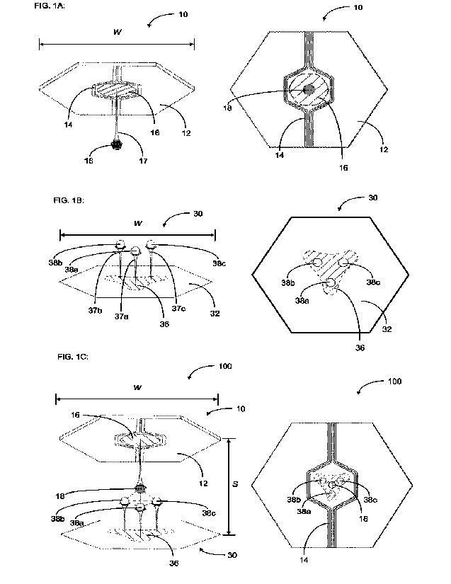
[0054] FIGs. 1A-1C and 2A-2D schematically
illustrate various aspects of example
multiple-qubit gates (e.g., cells) in accordance with certain implementations
described herein.
The qubit gates are formed by interspersing electropotential wells both above
and below
parallel surface planes and using the electropotential wells to trap ions that
are entangled with
other trapped ions. Examples of ions compatible with certain implementations
described
herein include but are not limited to: Bat; Be; Cd ; Cat; MC; He; Si'; Ybt
Vertical
orientation is not required, so the terms "top" and "bottom" are not used.
[0055] FIG. IA schematically illustrates a
side-angle view and a top view of an
example single-ion portion 10 of an example four-ion qubit gate 100 in
accordance with certain
implementations described herein. The single-ion portion 10 comprises a
substantially planar
substrate region 12, one or more electrical traces 14, an electrode region 16
comprising one or
more electrodes (not shown), an electropotential well 17, and a single ion 18.
In certain
implementations, the substrate region 12 comprises a portion of an electrical
insulator and/or
semiconductor (e.g., silicon oxide; silicon) chip, and at least some of the
electrical traces 14
-16-
CA 03157734 2022-5-9
WO 2021/092233
PCT/US2020/059192
are in electrical communication with the electrodes of the electrode region
16. At least some
of the other electrical traces 14 can be in electrical communication with the
electrodes of the
electrode regions of portions of other neighboring qubits. For example, the
electrical traces 14
and the electrodes within the electrode region 16 can comprise electrically
conductive material
(e.g., aluminum; copper; gold) deposited onto a surface of the substrate
region 12, and can
comprise at least one hermetic coating configured to hermetically seal the
electrically
conductive material from contaminants and/or corrosion. The electrodes of the
electrode
region 16 are configured to generate the electropotential well 17 which is
configured to contain
(e.g., suspend; trap) the single ion 18 at a position spaced away from the
planar substrate region
12 (e.g., in a direction substantially perpendicular to the substrate region
12).
[0056]
FIG. 1B schematically
illustrates a side-angle view and a top view of an
example three-ion portion 30 of the example four-ion qubit gate 100 in
accordance with certain
implementations described herein. The three-ion portion 30 comprises a
substantially planar
substrate region 32, one or more electrical traces (not shown), an electrode
region 36
comprising multiple electrodes (not shown), three electropotential well 37a-c,
and three ions
38a-c. In certain implementations, the substrate region 32 comprises a portion
of an electrical
insulator and/or semiconductor (e.g., silicon oxide; silicon) chip, and at
least some of the
electrical traces are in electrical communication with the electrodes of the
electrode region 36.
At least some of the other electrical traces can be in electrical
communication with the
electrodes of the electrode regions of other portions of neighboring qubits.
For example, the
electrical traces and the electrodes within the electrode region 36 can
comprise electrically
conductive material (e.g., aluminum; copper; gold) deposited onto a surface of
the substrate
region 32, and can comprise at least one hermetic coating configured to
hermetically seal the
electrically conductive material from contaminants and/or corrosion.
In certain
implementations, electrical traces 14 that are in electrical communication
with electrodes
within region 36 or other electrode regions can be in substrate layers (not
shown) beneath the
surface (e.g., sub-surface) and can run substantially consistently with other
electrical traces 14
on the surface. The electrodes of the electrode region 36 are configured to
generate the three
electropotential wells 37a-c, each of which is configured to contain (e.g.,
suspend; trap) a
corresponding one of the three ions 38a-c at a position spaced away from the
planar substrate
region 32 (e.g., in a direction substantially perpendicular to the substrate
region 32). In certain
-17-
CA 03157734 2022-5-9
WO 2021/092233
PCT/US2020/059192
implementations, the three ions 38a-c form an equilateral triangle (e.g.,
spaced from one
another by a distance in a range of 30 microns to 40 microns), with the
triangle substantially
parallel to the substrate region 32. The three ions 38a-c of the triangle are
an example of three
qubits arranged in a substantially planar region and configured to interact
with one another in
accordance with certain implementations described herein.
[0057] In certain implementations, as shown in
FIGs. 1A-1B, the substrate region
12 of the single-ion portion 10 and the substrate region 32 of the three-ion
portion 30 (e.g., the
portions of the respective chips that generally correspond to the four-ion
qubit gate 100) have
a substantially hexagonal shape, while in certain other implementations, the
substrate regions
12,32 have other shapes (e.g., rectangular, square; triangular; circular;
oval; geometric; non-
geometric; symmetric; non-symmetric).
[0058] The hashed regions of FICrs. 1A and 1B
corresponding to the electrode
regions 16,36 (e.g., electrode patch zones) represent general "write" zones
that an positioned
and shaped to accommodate the multiple individual electrodes within each zone
for generating
the electropotential wells 17, 37a-c for confining the corresponding ions 18,
38a-c. The
positioning and shaping of the various electrodes for the particular
configurable gate
implementation can be designed using algorithms (e.g., as provided by Schmied
2009). In
certain implementations, the electrode regions 16,36 are configured to trap,
fully control, and
perform gate operations using the corresponding ions 18, 38a-c. For example,
the electrode
region 36 of FIG. 1B can include eight or more electrodes per ion trap zone.
In certain
implementations, the electrodes and the electrode regions 16, 36 are based on
previously
developed electrodes and electrode regions for 2-D layouts for trapped ions
(see, e.g., C.W.
Hogle et al_, "Characterization of Microfabricated Surface Ion Traps," Sandia
National Lab.,
SAND2017-6113C (2017)).
[0059] FIG. IC schematically illustrates a
side-angle view and a top view of the
example four-ion qubit gate 100 comprising the single-ion portion 10 of FIG.
1A (e.g., as a
"cap" of the four-ion qubit gate 100) and the three-ion portion 30 of FIG. 1B
(e.g., as a "base"
of the four-ion qubit gate 100), with the ions 18, 38a-c configured to be
fully-connected to one
another and/or to ions of neighboring qubit gates (e.g., simultaneously or in
any subset
combination), in accordance with certain implementations described herein. The
example
four-ion qubit gate 100 of FIG. IA has a substantially hexagonal shape, while
in certain other
-18-
CA 03157734 2022-5-9
WO 2021/092233
PCT/US2020/059192
implementations, the qubit gate 100 has other shapes (e.g., rectangular;
square; triangular;
circular; oval; geometric; non-geometric; symmetric; non-symmetric).
In certain
implementations, the qubit gate 100 has a width W (e.g., in a range of less
than or equal to
0.2 nun). While the right-side of FIG. IC shows at least some of the
electrical traces 14 on the
surface of the portion 30, in certain implementations, at least some of the
electrical traces 14
are in substrate layers (not shown) beneath the surface (e.g., sub-surface)
and can run
substantially consistently with other electrical traces 14 on the surface. In
certain
implementations, the substrate region 12 is substantially parallel to the
substrate region 32 and
the substrate region 12 is spaced from the substrate region 32 by a distance S
(e.g., in a range
less than or equal to 0.2 mm). In certain implementations, the single ion 18
is spaced from
each of the three ions 38a-c (e.g., by a distance in a range of 30 microns to
45 microns) and is
positioned above the center of the triangle formed by the three ions 38a-c.
Each of the ions
18, 38a-c is entangled with each of the other ions 18, 38a-c, as denoted by
the dashed lines in
FIG. 1C. In certain implementations, the example four-ion qubit gate 100 has a
width W(e.g.,
in a range of less than or equal to 0.2 mm). The three ions 38a-c are an
example of three qubits
arranged in a first substantially planar region (e.g., the distances of the
three ions 38a-c from
the substrate region 32 can be within 5 microns, within 2 microns, and/or
within 1 micron
of one another) and the single ion 18 is an example of a qubit arranged in a
second substantially
planar region substantially parallel to the first substantially planar region.
The qubit of the
second substantially planar region is configured to interact with the three
qubits of the first
substantially planar region which are configured to interact with one another,
in accordance
with certain implementations described herein_
[0060]
In certain implementations,
the example four-ion qubit gate 100 of FIG. 1C
is used as a "native" C3NOT gate (e.g., a triply-controlled NOT gate) and/or
as "native" C3q)
gate (e.g., a triply-controlled phase gate). The example four-ion qubit gate
100 of certain
implementations can effect a C3NOT/C39 gate with significantly fewer gate
operations than
would be used by one- or two-qubit gates alone. In certain implementations,
the net fidelity
of the native C3NOT/C39 gate provided by the example four-ion qubit gate 100
is significantly
greater than that of a C3NOT/C3c, gate comprising many two-qubit gates that
may have much
higher individual gate fidelities, since the four-ion qubit gate 100 does not
aggregate the errors
of many successive operations to achieve its result_ In certain such
implementations, the
-19-
CA 03157734 2022-5-9
WO 2021/092233
PCT/US2020/059192
C3NOT/C39 gate provided by the example four-ion qubit gate 100 uses a fraction
of the steps
of a C3NOT/C3p gate comprising many two-qubit gates, so the C3NOT/C3p gate
provided by
the example four-ion qubit gate 100 is faster and less error-prone (e.g.,
thereby utilizing
significantly less error correction at the outset), as can be seen in a
comparison of the
probabilities of successful gate operation using both structures and fidelity
estimates.
[0061] FIG. 2A schematically illustrates a
side-angle view of an example seven-
ion qubit gate 200 in accordance with certain implementations described
herein. In certain
implementations, the example seven-ion qubit gate 200 of FIG. 2A is configured
to be used as
a native C6NOT/C69 gate. The example seven-ion qubit gate 200 of FIG. 2A
comprises the
single-ion portion 10 of FIG. lA (e.g., as a "cap" of the seven-ion qubit gate
200) and a six-
ion portion 50 (e.g., as a "base" of the seven-ion qubit gate 200). The six-
ion portion 50
comprises a planar substrate region 52, one or more electrical traces (not
shown), six electrode
regions 56a-f, six electropotential wells 57a-f, and six ions 58a-f. The
electrodes of the
electrode regions 56a-f are configured to generate the six electropotenfial
wells 57a-f, each of
which is configured to contain (e.g., suspend; trap) a corresponding one of
the six ions 58a-f
at a position spaced away from the planar substrate region 52 (e.g., in a
direction substantially
perpendicular to the substrate region 52). As schematically illustrated by
FIG. 2A, the example
seven-ion qubit gate 200 can comprise an additional electrode 59 (e.g., a
cover electrode) (see,
e.g., C.E. Pearson et al., Phys. Rev. A Vol. 73, 032307 (2006)) positioned
below the single ion
18 of the single-ion portion 10 and configured to aid tuning of the distance
of the single ion 18
relative to the six-ion portion 50. In certain implementations, the six ions
58a-f form an
equilateral hexagon (e.g., spaced from one another by a distance in a range of
35 microns to
70 microns), with the hexagon substantially parallel to the substrate region
52. The spacing of
the hexagons from one another can be set based on various parameters,
including but not
limited to: multiple tuning parameters, ion species, crystal lattice angles
formed. In certain
implementations, the distance of each qubit in the hexagon from the nearest
substrate can have
variability (e.g., at a nominal distance of 40 microns 5 microns), as a
result of 3-E1 angles in
the crystal lattice. The seven ions 18, 58a-f are configured to be fully
connected to one another
and/or to ions of neighboring qubit gates (e.g., simultaneously, or in any
subset combination),
as schematically illustrated by the dotted lines which denote entanglements
among the seven
ions 18, 58a-f. As schematically illustrated in FIG. 2A, in certain
implementations, portions
-20-
CA 03157734 2022-5-9
WO 2021/092233
PCT/US2020/059192
of the electrode regions 56a-f of the six-ion portion 50 extend onto the
substrate regions of the
bases of neighboring qubits and portions of the electrode regions of
neighboring portions
extend onto the substrate region 12 of the single-ion portion 10. The six ions
58a-f are an
example of six qubits arranged substantially in a first substantially planar
region (e.g., the
distances of the six ions 58a-f from the substrate portion 52 can be within 5
microns, within
2 microns, and/or within 1 micron of one another) and the single ion 18 is
an example of a
qubit arranged in a second substantially planar region substantially parallel
to the first
substantially planar region. The qubit of the second substantially planar
region is configured
to interact with the six qubits of the first substantially planar region which
are configured to
interact with one another, in accordance with certain implementations
described herein.
[0062]
In certain implementations,
the single ion 18 is contained (e.g., suspended;
trapped) in a first electropotential well 17, the single ion 18 at a first
distance (e.g., 40 microns)
from the electrode region 16. In certain other implementations, the single ion
18 is contained
in a second electropotential well, the single ion 18 at a second distance from
the substrate
region 52, the second distance approximately twice the first distance (e.g.,
80 microns). For
example, the second electropotential well can be formed naturally (see, e.g.,
M. Mielenz et al.,
"Arrays of individually controlled ions suitable for two-dimensional quantum
simulations,"
Nature Communications, 7:11839 (2016)).
In certain implementations,
the first
electropotential well 17 and the second electropotential well coincide or
overlap with one
another such that the single ion 18 is contained in both the first and second
electropotential
wells concurrently, while in certain other implementations, the first and
second electropotential
wells are separate from one another.
[0063]
FIG. 2B schematically
illustrates a side-angle view and a top view of an
example eight-ion qubit gate 300 in accordance with certain implementations
described herein.
In certain implementations, the example eight-ion qubit gate 300 of FIG. 2B is
configured to
be used up to a CNOT/Cip gate. The example eight-ion qubit gate 300 of FIG. 2B
comprises
the single-ion portion 10 of FIG. 1A (e.g., as a "cap" of the eight-ion qubit
gate 300) and a
seven-ion portion 70 (e.g., as a "base" of the eight-ion qubit gate 300). The
seven-ion portion
70 comprises a planar substrate region 72, one or more electrical traces (not
shown), seven
electrode regions 76a-g, seven electropotential wells 77a-g, and seven ions
78a-g. The
electrodes of the electrode regions 76a-g are configured to generate the seven
electropotential
-21-
CA 03157734 2022-5-9
WO 2021/092233
PCT/US2020/059192
wells 77a-g, each of which is configured to contain (e.g., suspend; trap) a
corresponding one
of the seven ions 78a-g at a position spaced away from the planar substrate
region 72 (e.g., in
a direction substantially perpendicular to the substrate region 72). The
example eight-ion qubit
300 of FIG. 2B is similar to the seven-ion qubit gate 200 of FIG. 2A, with the
addition of the
eighth electrode region 76g, eighth electropotential well 77g, and eighth ion
78g (e.g.,
positioned in a range of 30 to 60 microns above the electrode region 76g). The
distance of the
eighth ion 78g from the substrate region 72 can be based on various factors,
including but not
limited to whether the seven-ion portion 70 is combined with a single-ion
portion 10, a three-
ion portion 30, or another multiple-ion portion as described herein. The eight
ions 18, 78a-g
are configured to be fully connected to one another and/or to ions of
neighboring qubit gates
(e.g., simultaneously, or in any subset combination) (dotted lines denoting
entanglements
among the eight ions 18, 78a-g are omitted from FIG. 2B for the sake of
clarity). The six ions
78a-f are an example of six qubits arranged substantially in a first
substantially planar region
(e.g., the distances of the six ions 78a-f from the substrate portion 72 can
be within 5 microns,
within th 2 microns, and/or within th 1 micron of one another), the seventh
ion 78g is an example
of a qubit arranged in a second substantially planar region substantially
parallel to the first
substantially planar region, and the single ion 18 is an example of a qubit
arranged in a third
substantially planar region substantially parallel to the first substantially
planar region. The
qubit of the second substantially planar region and the qubit of the third
substantially planar
region are configured to interact with one another and with the six qubits of
the first
substantially planar region which are configured to interact with one another,
in accordance
with certain implementations described herein.
[0064] With regard to the example seven-ion
qubit gate 200 of FIG. 2A and the
example eight-ion qubit gate 300 of FIG. 2B, in certain implementations, each
of the qubit
gates 200,300 has a substantially hexagonal shape, while in certain other
implementations, the
qubit gates 200, 300 have other shapes (e.g., rectangular; square; triangular;
circular; oval;
geometric; non-geometric; symmetric; non-symmetric). In certain
implementations, the
substrate region 52, 72 comprises a portion of an electrical insulator and/or
semiconductor
(e.g., silicon oxide; silicon) chip, at least some of the electrical traces
are in electrical
communication with the electrodes of the electrode regions 56, 76 and other
electrical traces
are in electrical communication with the electrode regions of other bases. In
certain
-22-
CA 03157734 2022-5-9
WO 2021/092233
PCT/US2020/059192
implementations, each of the electrode regions 56, 76 comprises one or more
electrodes in
electrical communication with at least some of the electrical traces, and the
electrical traces
and the electrodes within the electrode regions 56,76 comprise electrically
conductive material
(e.g., aluminum; copper; gold) deposited onto a surface of the substrate
region 52, 72, and can
comprise at least one hermetic coating configured to hermetically seal the
electrically
conductive material from contaminants and/or corrosion. The electrodes of the
electrode
regions 56, 76 of certain implementations are configured to at least partially
extend into
neighboring regions (e.g., regions of neighboring qubits) and to provide space
for the electrical
traces to run to the electrode region of the qubit gate 200,300 and/or to the
neighboring qubits.
In certain implementations, the seven-ion qubit gate 200 and/or the eight-ion
qubit gate 300
has a width W (e.g., in a range of less than or equal to 0.2 mm), the
substrate region 12 is
substantially parallel to the substrate region 52, 72, and the substrate
region 12 is spaced from
the substrate region 52, 72 by a distance S (e.g., in a range less than or
equal to 0.2 mm).
100651 FIG. 2C schematically illustrates a
side-angle view of an example nine-ion
qubit gate 400 in accordance with certain implementations described herein. In
certain
implementations, the nine-ion qubit gate 400 can aid cross-chip connectivity
(e.g., in a QFPGA
architecture or in a QASIC architecture). In certain implementations, the
example nine-ion
qubit gate 400 of FIG. 2C can also be configured to be used in multiply-
controlled gate
operations or to employ combinations of redundant control and/or target qubits
to facilitate
self-error-correcting gates at desired nodes. The example nine-ion qubit gate
400 of FIG. 2C
comprises the six-ion portion 50 of FIG. 2A (e.g., as a "cap" of the nine-ion
qubit gate 400)
and the three-ion portion 30 (e.g., as a "base" of the nine-ion qubit gate
400). The nine ions
38a-c, 58a-f are configured to be fully connected to one another and/or to
ions of neighboring
qubit gates (e.g., simultaneously, or in any subset combination) (dotted lines
denoting
entanglements among the nine ions 38a-c, 58a-f are omitted from FIG. 2C for
the sake of
clarity). The six ions 58a-f are an example of six qubits arranged
substantially in a first
substantially planar region (e.g., the distances of the six ions 58a-f from
the substrate portion
52 can be within 5 microns, within 2 microns, and/or within 1 micron of
one another)
and the three ions 38a-c are an example of three qubits arranged in a second
substantially planar
region (e.g., the distances of the three ions 38a-c from the substrate portion
32 can be within
microns, within 2 microns, and/or within 1 micron of one another)
substantially parallel
-23-
CA 03157734 2022-5-9
WO 2021/092233
PCT/US2020/059192
to the first substantially planar region. The six qubits 58a-f of the first
substantially planar
region are configured to interact with one another, and the three qubits 38a-c
of the second
substantially planar region are configured to interact with one another and
with qubits of the
first substantially planar region in accordance with certain implementations
described herein.
In certain implementations, the three ions 38a-c and/or the six ions 58a-f are
further configured
to interact with ions of other qubit gates neighboring the nine-ion qubit gate
400 (e.g., intercell
interactions).
[0066] FIG. 2D schematically illustrates a
side-angle view of an example ten-ion
qubit gate 450 in accordance with certain implementations described herein. In
certain
implementations, the ten-ion qubit gate 450 can aid cross-chip connectivity
(e.g., in a QFPGA
architecture or in a QASIC architecture). In certain implementations, the
example ten-ion qubit
gate 450 of FIG. 2D can also be configured to be used in multiply-controlled
gate operations
(e.g., up to a C9NOT/C9T gate) or to employ combinations of redundant control
and/or target
qubits to facilitate self-error-correcting gates at desired nodes. The example
ten-ion qubit gate
450 of FIG. 2D comprises the seven-ion portion 70 of FIG. 2B (e.g., as a "cap"
of the ten-ion
qubit gate 450) and the three-ion portion 30 (e.g., as a "base" of the ten-ion
qubit gate 450).
The ten ions 38a-c, 78a-g are configured to be fully connected to one another
and/or to ions of
neighboring qubit gates (e.g., simultaneously, or in any subset combination)
(dotted lines
denoting entanglements among the nine ions 38a-c, 78a-g are omitted from FIG.
2D for the
sake of clarity). The six ions 78a-f are an example of six qubits arranged
substantially in a first
substantially planar region (e.g., the distances of the six ions 78a-f from
the substrate portion
72 can be within t 5 microns, within th 2 microns, and/or within th 1 micron
of one another),
the seventh ion 78g is an example of a qubit arranged in a second
substantially planar region
substantially parallel to the first substantially planar region, and the three
ions 38a-c are an
example of three qubits arranged in a third substantially planar region (e.g.,
the distances of
the three ions 38a-c from the substrate portion 32 can be within 5 microns,
within th 2
microns, and/or within + 1 micron of one another) substantially parallel to
the first substantially
planar region. The six qubits 78a-f of the first substantially planar region
are configured to
interact with one another, the three qubits 38a-c of the third substantially
planar region are
configured to interact with one another, as well as with qubits of the first
substantially planar
region, and the single qubit of the second substantially planar region is
configured to interact
-24-
CA 03157734 2022-5-9
WO 2021/092233
PCT/US2020/059192
with qubits of the first substantially planar region and qubits of the second
substantially planar
region, in accordance with certain implementations described herein.
In certain
implementations, the three ions 38a-c and/or the seven ions 78a-g are further
configured to
interact with ions of other qubit gates neighboring the ten-ion qubit gate 450
(e.g., intercell
interactions).
[0067]
FIG. 2E schematically
illustrates two side-angle views of an example
thirteen-ion qubit gate 500 (e.g., a "pyrochlore" cell) in accordance with
certain
implementations described herein. In certain implementations, the example
thirteen-ion qubit
gate 500 of FIG. 2E is configured to be used up to a Cl2NOT/C12, gate. The
example thirteen-
ion qubit gate 500 of FIG. 2E comprises the seven-ion portion 70 of FIG. 2B
(e.g., as a "cap"
of the thirteen-ion qubit gate 500), with an increase in length of the
electropotential well 77g,
and concomitant distance of the ion 78g from the electrode region 76g, along
with the six-ion
portion 50 (e.g., as a "base" of the thirteen-ion gate qubit 500). The
thirteen ions 58a-f, 78a-g
are configured to be fully connected to one another and/or to ions of
neighboring qubit gates
(e.g., simultaneously, or in any subset combination) (dotted lines denoting
entanglements
among the thirteen ions 58a- 78a-g are omitted from FIG. 2E for the sake of
clarity). The six
ions 58a-f are an example of six qubits arranged substantially in a first
substantially planar
region 502 (e.g., the distances of the six ions 58a-f twin the substrate
portion 52 can be within
microns, within 2 microns, and/or within cE 1 micron of one another; at a
distance Hi of
about 40 microns from the substrate portion 52), the six ions 78a-f are an
example of six qubits
arranged substantially in a second substantially planar region 504 (e.g., the
distances of the six
ions 78a-f from the substrate portion 72 can be within 5 microns, within 2
microns, and/or
within 1 micron of one another; at a distance Hi of about 40 microns from
the substrate
portion 72) substantially parallel to the first substantially planar region
502, and the single ion
18 is an example of a qubit arranged in a third substantially planar region
506 substantially
parallel to the first substantially planar region 502 (e.g., at a distance H2
in a range of
50 microns to 60 microns from the substrate portion 72). The six qubits of the
first
substantially planar region 502 are configured to interact with one another,
the six qubits of
the second substantially planar region 504 are configured to interact with one
another and with
the six qubits of the first substantially planar region 502, and the qubit of
the third substantially
planar region 506 is configured to interact with qubits of the first
substantially planar region
-25-
CA 03157734 2022-5-9
WO 2021/092233
PCT/US2020/059192
502 and with qubits of the second substantially planar region 504, in
accordance with certain
implementations described herein. In certain implementations, the six ions 58a-
f and/or the
seven ions 78a-g are further configured to interact with ions of other qubit
gates neighboring
the thirteen-ion qubit gate 500 (e.g., intercell interactions).
[0068] FIG. 2F schematically illustrates two
side-angle views of an example
fourteen-ion qubit gate 550 in accordance with certain implementations
described herein. In
certain implementations, the example fourteen-ion qubit gate 550 of FIG. 2F is
configured to
be used up to a Ci3NOT/C", gate. The example fourteen-ion qubit gate 550 of
FIG. 2F
comprises a first seven-ion portion 70 (see, e.g., FIG. 213) (e.g., as a "cap"
of the fourteen-ion
qubit gate 550), with the ion 78g and the electropotential well 77g of the
first seven-ion portion
70 a longer distance from the substrate portion 72 than are the ion 78g and
the electropotential
well 77g of FIG. 213. The example fourteen-ion qubit gate 550 of FIG. 2F
further comprises a
second seven-ion portion 70 (see, e.g., FIG. 2B) (e.g., as a "base" of the
fourteen-ion gate qubit
gate 550), with the ion 78g and the electropotential well 77g of the second
seven-ion portion
70 a shorter distance from the substrate portion 72 than are the ion 78g and
the electropotential
well 77g of FIG. 213. The first set of ions 78a-g of the first seven-ion
portion 70 and the second
set of ions 78a-g of the second seven-ion portion 70 are configured to be
fully connected to
one another and/or to ions of neighboring qubit gates (e.g., simultaneously,
or in any subset
combination) (dotted lines denoting entanglements among the first set of ions
78a-g and the
second set of ions 78a-g are omitted from FIG. 2F for the sake of clarity).
[0069] The six ions 78a-f in the "base" are an
example of six qubits arranged
substantially in a first substantially planar region 552 (e.g., the distances
of the six ions 78a-f
from the substrate portion 72 can be within 5 microns, within th 2 microns,
and/or within th 1
micron of one another; at a distance Hi of about 40 microns from the substrate
portion 72), the
six ions 78a-f in the "cap" are an example of six qubits arranged
substantially in a second
substantially planar region 554 (e.g., the distances of the six ions 78a-f
from the substrate
portion 72 can be within 5 microns, within th 2 microns, and/or within th 1
micron of one
another; at a distance Hi of about 40 microns from the substrate portion 72)
substantially
parallel to the first substantially planar region 552, one ion 78g above the
base is an example
of a qubit arranged in a third substantially planar region 556 substantially
parallel to the first
substantially planar region 552 (e.g., at a distance H2 in a range of 30
microns to 40 microns
-26-
CA 03157734 2022-5-9
WO 2021/092233
PCT/US2020/059192
from the substrate portion '72), and one ion 78g below the cap is an example
of a qubit arranged
in a fourth substantially planar region 558 substantially parallel to the
second substantially
planar region 554 (e.g., at a distance H3 in a range of 50 microns to 60
microns from the
substrate portion 72). The qubits of the first substantially planar region 552
are configured to
interact with one another, the qubits of the second substantially planar
region 554 are
configured to interact with one another and with qubits of the first
substantially planar region
552. The qubit of the third substantially planar region 556 is configured to
interact with the
qubits of the first substantially planar region 552 and with the qubits of the
second substantially
planar region 554. The qubit of the fourth substantially planar region 558 is
configured to
interact with qubits of the first substantially planar region 552, with qubits
of the second
substantially planar region 554, and with the qubit of the third substantially
planar region 556
in accordance with certain implementations described herein. In certain
implementations, the
first set of ions 78a-g and/or the second set of ions 78a-g are further
configured to interact with
ions of other qubit gates neighboring the fourteen-ion qubit gate 550 (e.g.,
intercell
interactions).
[0070] The examples provided correspond to
configurations configured to be
employed in the pluralities of multi-qubit gate array implementations that
follow (e.g., as
QFPGA or QASIC implementations) for ease of discussion. Other cell
combinations of the
"cap" and "base" are also compatible with certain implementations described
herein. For
example, in a QASIC implementation, it can be advantageous to combine the
seven-ion portion
70 of FIG. 2B, modified by an increase or decrease in length of the
electropotential well 77g,
and concomitant distance of the ion 78g from the electrode region 76g as
described above, to
create a fourteen-ion qubit gate that can be used up to a C 13NOT/C13, gate as
schematically
illustrated in FIG. 2R In addition, these and other numbers of qubits (e.g.,
1, 2, 3, 4, 5, 6, 7,
8, 9, 10, or more qubits) per first portion 810 and/or per second portion 820
are compatible
with certain implementations described herein.
[0071] Certain implementations described
herein provide a quantum computing
(QC) system 1000 comprising a substantially planar first substrate 600 and a
substantially
planar second substrate 700, the first substrate 600 and the second substrate
700 substantially
parallel to one another. The quantum computing system 1000 further comprises a
multiple-
qubit gate array 800 comprising a plurality of multiple-qubit gates 802
positioned in a region
-27-
CA 03157734 2022-5-9
WO 2021/092233
PCT/US2020/059192
between the first substrate 600 and the second substrate 700. Each multiple-
qubit gate 802 of
the array 800 comprises a first (e.g., base) portion 810 at (e.g., above;
below; on) a surface of
the first substrate 600 and a second (e.g., cap) portion 820 at (e.g., above;
below; on) a surface
of the second substrate 700 and the qubits interact with one another between
the surfaces of
the first and second substrates 600, 700. The first portion 810 of each
multiple-qubit gate 802
of the array 800 is selected from the group consisting of: a single-qubit
portion 10, a three-
qubit portion 30, a six-qubit portion 50, and a seven-qubit portion 70. The
first portions 810
are arranged along the surface of the first substrate 600 (e.g., the substrate
regions 12, 32, 52,
72 of the single-qubit portions 10, three-qubit portions 30, six-qubit
portions 50, and seven-
qubit portions 70 are regions of the first substrate 600). The second portion
820 of each
multiple-qubit gate 802 of the array 800 is selected from the group consisting
of: a single-qubit
portion 10, a three-qubit portion 30, a six-qubit portion 50, and a seven-
qubit portion 70. The
second portions 820 are arranged along the surface of the second substrate 700
(e.g., the
substrate regions 12, 32, 52, 72 of the single-qubit portions 10, three-qubit
portions 30, six-
qubit portions 50, and seven-qubit portions 70 are regions of the second
substrate 700). For
each multiple-qubit gate 802, each qubit of the first portion 810 and of the
second portion 820
of the multiple-qubit gate 802 is configured to be quantum-mechanically
entangled with each
of the other qubits of the first portion 810 and the second portion 820 of the
multiple-qubit gate
802.
[0072] FIG. 3A schematically illustrates a top
view of four example first portions
810 (e.g., bases) of an example array 800 comprising four multiple-ion qubit
gates (e.g., cells)
802 in accordance with certain implementations described herein. The four
first portions 810
of FIG_ 3A comprise a one-ion portion 10, a three-ion portion 30, a six-ion
portion 50, and a
seven-ion portion 70. These four first portions 810 are tiled together with
their respective
substrate regions 12, 32, 52, 72 each part of a common first substrate 600
(e.g., the substrate
regions 12, 32, 52, 72 are coplanar with one another at a surface of the first
substrate 600).
The tiling includes a rhomboid region 830 bounded by the four first portions
810. As shown
in FIG. 3A, at least some of the electrode regions of the six-ion portion 50
and the seven-ion
portion 70 (e.g., electrode regions 56a-f, 76a-f) extend to neighboring first
portions 810 and/or
the rhomboid region 830. In certain implementations, the first portions 810 in
adjacent rows
are configured to facilitate tiling the first portions 810 close together
(e.g., without the electrode
-28-
CA 03157734 2022-5-9
WO 2021/092233
PCT/US2020/059192
regions overlapping one another). While FIG. 3A shows the first portions 810
in a substantially
rectangular pattern, the first portions 810 of other implementations can be in
a substantially
hexagonal pattern or a substantially diagonal pattern. Furthermore, while the
first portions 810
of FIG. 3A are schematically illustrated as a 2 x 2 array, other tiling
combinations of two, three,
or more portions in arrays are also compatible with certain implementations
described herein.
For example, the first portions 810 can be tiled in arrays that are linear
(e.g., 1 x 2, 1 x 3, or
more), square or rectangular (e.g., 2 x 3, 3 x 3, 2 x 4, 3 x 4, 4 x 4, 2 x 5,
etc.), and other
geometries that can be regular or irregular (e.g., similar to domino tiling)
and/or symmetric or
non-symmetric.
[0073] FIG. 3B schematically illustrates a top
view of four example second
portions 820 (e.g., caps) of the example array 800 and four multiple-ion qubit
gates 802 in
accordance with certain implementations described herein. The four second
portions 820 of
FIG. 3B comprise a one-ion portion 10, a three-ion portion 30, a six-ion
portion 50, and a
seven-ion portion 70. These four second portions 820 are filed together with
their respective
substrate regions 12, 32, 52, 72 each part of a common second substrate 700
(e.g., the substrate
regions 12, 32, 52, 72 are coplanar with one another at a surface of the
second substrate 700).
The tiling includes a rhomboid region 840 bounded by the four first portions
820. As shown
in FIG. 3B, at least some of the electrode regions of the six-ion portion 50
and the seven-ion
portion 70 (e.g., electrode regions 56a-f, 76a-f) extend to neighboring second
portions 820
and/or the rhomboid region 840. In certain implementations, the second
portions 820 in
adjacent rows are configured to facilitate tiling the second portions 820
close together (e.g.,
without the electrode regions overlapping one another). While FIG. 313 shows
the second
portions 820 in a substantially rectangular pattern, the second portions 820
of other
implementations can be in a substantially hexagonal pattern or a substantially
diagonal patient
Furthermore, while the second portions 820 of FIG. 3B are schematically
illustrated as a 2 x 2
array, other tiling combinations of two, three, or more portions in arrays,
and which coincide
with the filing of the first portions 810, are also compatible with certain
implementations
described herein. For example, the second portions 820 can be tiled in arrays
that are linear
(e.g., 1 x 2, 1 x 3, or more), square or rectangular (e.g., 2 x 3, 3 x 3, 2 x
4, 3 x 4, 4 x 4, 2 x 5,
etc.), and other geometries that can be regular or irregular (e.g., similar to
domino tiling) and/or
symmetric or non-symmetric.
-29-
CA 03157734 2022-5-9
WO 2021/092233
PCT/US2020/059192
[0074] FIGs. 3C-3D schematically illustrates
an exploded view and a top overlay
view, respectively, of the example array 800 and four multiple-ion qubit gates
802 of FIGs.
3A-3B in accordance with certain implementations described herein. The four
multiple-ion
qubit gates 802 comprise two four-ion qubit gates 100 and two thirteen-ion
qubit gates 500
between the first substrate 600 and the second substrate 700. One of the four-
ion qubit gates
100 comprises a three-ion base portion 30 and a one-ion cap portion 10,
another of the four-
ion qubit gates 100 comprises a one-ion base portion 10 and a three-ion cap
portion 30, one of
the thirteen-ion qubit gates 500 comprises a seven-ion base portion 70 and a
six-ion cap portion
50, and another of the thirteen-ion qubit gates 500 comprises a six-ion base
portion 50 and a
seven-ion cap portion 70. As described herein with regard to FIGs. 3A and 3B,
other tiling
combinations of the bases and caps into 3-D gate cell layouts can be used.
[0075] FIG. 3E schematically illustrate an
exploded view of another example array
800 with four multiple-ion qubit gates 802 in accordance with certain
implementations
described herein. The four multiple-ion qubit gates 802 comprise four ten-ion
qubit gates 450
between the first substrate 600 and the second substrate 700. Two of the ten-
ion qubit gates
450 each comprises a three-ion base portion 30 and a seven-ion cap portion 70,
and the other
two ten-ion qubit gates 450 each comprises a seven-ion base portion 70 and a
three-ion cap
portion 30. In the 2 x 2 array of the substrate 600, the three-ion base
portions 30 and seven-
ion base portions 70 alternate with one another and in the 2 x 2 array of the
substrate 700, the
seven-ion cap portions 70 and three-ion cap portions 30 alternate with one
another. The
electrical trace line layouts shown in FIG. 3E are different from those of
FIGs. 3C-3D.
[0076] FIGs. 4A-4B schematically illustrate an
exploded view and a top overlay
view, respectively, of an example array 900 comprising sixteen multiple-ion
qubit gates 902
in a 4 x 4 array in accordance with certain implementations described herein.
Other multi-
qubit gate arrays with different numbers of qubit gate arrays (e.g., more than
sixteen) and/or
in different geometric configurations (e.g., linear; rectangular; square;
regular; irregular;
symmetric; non-symmetric) are also compatible with certain implementations
described
herein. The sixteen multiple-ion qubit gates 902 of the array 900 are arranged
substantially in
a rectangular pattern with four rows each having four multiple-ion qubit gates
902 and four
columns each having four multiple-ion qubit gates 902. The multiple-ion qubit
gates 902 of
each row comprise two four-ion qubit gates 100 and two thirteen-ion qubit
gates 500 arranged
-30-
CA 03157734 2022-5-9
WO 2021/092233
PCT/US2020/059192
alternately (e.g., "4-13-4-13") and the multiple-ion qubit gates 902 of each
column comprise
two four-ion qubit gates 100 and two thirteen-ion qubit gates 500 arranged
alternately (e.g.,
"4-13-4-13"). The first (e.g., base) portions 810 of the array 900 are
arranged such that any
four nearest-neighboring first portions 810 comprise a one-ion portion 10, a
three-ion portion
30, a six-ion portion 50, and a seven-ion portion 70, and the second (e.g.,
cap) portions 820 of
the array 900 are arranged such that any four nearest-neighboring second
portions 820
comprise a one-ion portion 10, a three-ion portion 30, a six-ion portion 50,
and a seven-ion
portion 70. In certain implementations, the layouts of the first portions 810
and second portions
820 of the array 900 (e.g., for a QFPGA) are configured to reduce (e.g.,
minimize) qubit-to-
qubit spacing and/or to optimize cell-to-cell connectivity.
[0077] As schematically illustrated in FIGs.
4A-4B, at least some of the electrical
traces 14 extending along the first substrate 600 and/or the second substrate
700 comprise
substantially straight sections that are substantially perpendicular to the
boundaries between
neighboring first portions 810 of the first substrate 600 and/or the
boundaries between
neighboring second portions 820 of the second substrate 700. For example, the
electrical traces
14 shown as being vertical in FIG. 4B are substantially perpendicular to the
horizontal
boundaries in FIG. 4B. FIG. 4C schematically illustrates a top overlay view of
another
example multiple-ion qubit gate array 900 with sixteen multiple-ion qubit
gates 902 in
accordance with certain implementations described herein. At least some of the
electrical
traces 14 extending along the first substrate 600 and/or the second substrate
700 in FIG. 4C
comprise substantially straight section that are not substantially
perpendicular to the
boundaries between neighboring first portions 810 of the first substrate
and/or the boundaries
between neighboring second portions 820 of the second substrate 700_ For
example, the
electrical traces 14 shown as being substantially vertical in FIG. 4C extend
over at least some
of the hexagonal boundaries in FIG. 4C but are not substantially perpendicular
to these
hexagonal boundaries. Other positions and/or orientations of the electrical
traces 14 are also
compatible with certain implementations described herein. For example, the
electrical traces
14 can be curved so as to create room for optical ports for entry and/or exit
of laser signals into
the region between the first substrate 600 and the second substrate 700.
[0078] FIG. 4D schematically illustrates a top
overlay view of another example
multiple-ion qubit gate array 800 comprising four multiple-ion qubit gates 802
in accordance
-31-
CA 03157734 2022-5-9
WO 2021/092233
PCT/US2020/059192
with certain implementation described herein. The four multiple-ion qubit
gates 802 comprise
two eight-ion qubit gates 300 (see, e.g., FIG. 2B) and two nine-ion qubit
gates 400 (see, e.g.,
FIG. 2C) between the first substrate 600 and the second substrate 700. One of
the eight-ion
qubit gates 300 comprises a seven-ion base portion 70 and a one-ion cap
portion 10, another
of the eight-ion qubit gates 300 comprises a one-ion base portion 10 and a
seven-ion cap
portion 70, one of the nine-ion qubit gates 400 comprises a three-ion base
portion 30 and a six-
ion cap portion 50, and another of the nine-ion qubit gates 400 comprises a
six-ion base portion
50 and a three-ion cap portion 30.
[0079] FIG. 4E schematically illustrates a top
overlay view of another example
multiple-ion qubit gate array 900 comprising sixteen multiple-ion qubit gates
902 in
accordance with certain implementations described herein. The sixteen multiple-
ion qubit
gates 902 of the array 900 are arranged substantially in a rectangular pattern
with four rows
each having four multiple-ion qubit gates 902 and four columns each having
four multiple-ion
qubit gates 902. The rows of the multiple-ion qubit gates 902 are arranged
alternately between
four nine-ion qubit gates 400 (e.g., 9-9-9-9) and four eight-ion qubit gates
300 (e.g., "8-8-8-
81 and the multiple-ion qubit gates 902 of each column comprise two nine-ion
quhit gates 400
and two eight-ion qubit gates 300 arranged alternately (e.g., "9-8-9-8"). In
certain
implementations, the layouts of the first portions 810 and second portions 820
of the array 900
(e.g., for a QFPGA) are configured to provide consistent spacing between ions
of neighboring
first portions 810 and second portions 820 of the array 900.
[0080] FIGs. 4F-4G schematically illustrate an
exploded view and a top overlay
view, respectively, of another example array 900 comprising sixteen multiple-
ion qubit gates
902 in a 4 x 4 array in accordance with certain implementations described
herein_ The sixteen
multiple-ion qubit gates 902 of the array 900 are arranged substantially in a
rectangular pattern
with four rows each having four multiple-ion qubit gates 902 and four columns
each having
four multiple-ion qubit gates 902. The multiple-ion qubit gates 902 of each
row comprise four
ten-ion qubit gates 450 and the multiple-ion qubit gates 902 of each column
comprise four ten-
ion qubit gates 450. The rows and columns of the first (e.g., base) portions
810 of the array
900 comprise three-ion portions 30 and seven-ion portions 70 arranged
alternately (e.g., "3-7-
3-7"), and the rows and columns of the second (e.g., cap) portions 820 of the
array 900 are
arranged alternately (e.g., "3-7-3-7"). In certain implementations, the
layouts of the first
-32-
CA 03157734 2022-5-9
WO 2021/092233
PCT/US2020/059192
portions 810 and second portions 820 of the array 900 are configured to
provide more uniform
spacing.
[0081] FIGs. 5A-5I schematically illustrate
various views of portions of example
QC structures 1000 in accordance with certain implementations described
herein. The example
QC structure 1000 can be used in a QASIC or a QFPGA layout. In certain
implementations,
the QC structure 1000 advantageously provides sufficient space for cooling
systems and
magnetic field systems for operating the QC structure 1000. In certain
implementations, the
overall configuration preserves channel space for electrical traces to control
multiple electrodes
per electrode region while advantageously addressing the problem of electrode
overlap, which
occurs between adjacent qubit gates in two-dimensional (2-D) layouts if they
are tiled closely
together (e.g., in an attempt to preserve usable coherence).
[0082] The example QC structure 1000 comprises
the example array 900 of FIG.
4C and with electrical traces 14 that are similar to those of FIG. 4C. In
certain
implementations, the alternating inverted cell rows of the base and/or cap
portions of the array
900 facilitate formation of electrical channels through which electrical
signals can be provided
to the ion traps of the array 900. For example, as shown in FIG_ 5A, the
electrical traces 14
are configured to provide electrical signals to the various electrodes of the
ion traps. Other
configurations of the cell rows and columns, electrical traces, as well as
cells with other
numbers of ions and/or qub its are also compatible with certain
implementations described
herein.
[0083] In certain implementations, the
alternating inverted cell rows of the base
and/or cap portions of the array 900 facilitate formation of optical channels
through which
optical signals can be inputted to and/or outputted from the ion traps of the
array 900. The
example QC structure 1000 further comprises a plurality of optical ports 905
in accordance
with certain implementations described herein. The plurality of optical ports
905 of the
example QC structure 1000 comprises a first plurality of optical ports 910 in
optical
communication with a first plurality of optical fibers 912, the first
plurality of optical ports 910
within the first portions 810 of the first substrate 600_ The plurality of
optical ports 905 of the
example QC structure 1000 further comprises a second plurality of optical
ports 920 in optical
communication with a second plurality of optical fibers 922, the second
plurality of optical
ports 920 within the second portions 820 of the second substrate 700_ At least
some of the
-33-
CA 03157734 2022-5-9
WO 2021/092233
PCT/US2020/059192
optical ports 910 are configured to emit optical signals 914 (e.g., pulses
generated by one or
more lasers, not shown) configured to irradiate specific ions of the array 900
(e.g., for
addressing and/or controlling specific qubits of the array 900) and at least
some of the optical
ports 920 are configured to emit optical signals 924 (e.g., pluses generated
by one or more
lasers, not shown) configured to irradiate specific ions of the array 900
(e.g., for addressing
and/or controlling specific qubits of the array 900). The plurality of optical
ports 905 of the
example QC structure 1000 further comprises a third plurality of optical ports
930 and a third
plurality of optical fibers 932. The optical ports 930 can be in optical
communication with the
third plurality of optical fibers 932, the third plurality of optical ports
930 positioned outside a
periphery of the array 900 and configured to emit optical signals 934 (e.g.,
pulses generated by
one or more lasers, not shown), the optical signals 934 configured to
irradiate specific ions of
the array 900 (e.g., for addressing and/or controlling specific qubits of the
array 900). In certain
implementations, the optical ports 910, 920, 930 comprise polished fiber ends
configured to
direct laser light signals 914, 924, 934 towards the corresponding specific
ions of the array
900.
[0084] The plurality of optical ports 905 of
the example QC structure 1000 further
comprises a fourth plurality of optical exit ports 940 within the first
portions 810 and/or the
second portions 820 and configured to allow light from the optical signals
914, 924 passing
the irradiated specific ions to exit or to be absorbed, so as to reduce (e.g.,
minimize) cross-talk
or other noise from light reflection or scattering towards unintended qubits.
The optical exit
ports 940 can comprise holes and/or light absorptive material.
[0085] The example QC structure 1000 further
comprises a plurality of optical
detectors 950 in optical communication with a fourth plurality of optical
fibers 952. The
plurality of optical detectors 950 (e.g., charge-coupled device (CCD) cameras;
superconducting single-photon nanowire detectors (SNSPDs); photomultiplier
tubes (PMTs);
bolometers) are configured to receive optical signals (e.g., fluorescent light
926) from ions of
the array 900 for reading out the status of the qubits of the array 900.
[0086] FIG. 5A schematically illustrates a top
view of the first portions 810 of the
example array 900 on the first substrate 600, with the second substrate 700
removed. As shown
in FIG. 5A, the electrical traces 14 can extend along the array 900 to provide
electrical
connectivity to the various electrodes of the first portions 810. The optical
ports 910 can be
-34-
CA 03157734 2022-5-9
WO 2021/092233
PCT/US2020/059192
positioned (e.g., interleaved) within the first portions 810 and oriented such
that the optical
signals 914 are directed towards specific ions of the second portions 820.
[0087] FIGs. 5B-5C schematically illustrate a
perspective view and a side view,
respectively, of the example QC structure 1000, including both the first and
second substrates
600,700 (e.g., multi-chip structure) of the example QC structure 1000.
[0088] FIG. 5D schematically illustrates a
perspective view (without the second
substrate 700) and a side view (with both the first substrate 600 and the
second substrate 700)
of the example QC structure 1000 with the optical signals 934 emitted from the
third plurality
of optical ports 930. These optical signals 934 are directed to ions 904
positioned at the center
of the multiple-ion qubit gates 902, which are at a different distance from
the first substrate
600 and the second substrate 700 than are the other non-center ions 906 of the
multiple-ion
qubit gates 902.
[0089] FIG. 5E schematically illustrates a
perspective view (without the optical
signals 914, 924), FIGs. 5F-5G schematically illustrate two side views of the
example QC
structure 1000, and FIG. 5H schematically illustrates another side view of the
example QC
structure 1000 in accordance with certain implementations described herein.
FIG_ 5F shows
three of the optical signals 914 emitted from three of the first plurality of
optical ports 910,
each of the three optical signals 914 directed to a corresponding ion of the
second portion 820
(e.g., a six-ion portion 50) of the multiple-ion qubit gate 902. In addition,
FIG. 5F shows the
optical signals 934 emitted from the third plurality of optical ports 930.
FIG. 56 shows six of
the optical signals 914 emitted from six of the first plurality of optical
ports 910, each of the
six optical signals 914 directed to a corresponding ion of the second portion
820 (e.g., a six-
ion portion 50) of the multiple-ion qubit gate 902. In addition, FIG_ 5G shows
the optical
signals 934 emitted from the third plurality of optical ports 930 and six of
the optical signals
924 emitted from six of the second plurality of optical ports 920, each of the
six optical signals
924 directed to a corresponding ion of the first portion 810 (e.g., a seven-
ion portion 70) of the
multiple-ion qubit gate 902. FIG. 511 shows the optical signals 924 emitted
from the second
plurality of optical ports 920 to irradiate corresponding ions, with some of
the light from the
optical signals 924 being allowed to exit via corresponding optical exit ports
940 (e.g., exiting
the region between the first and second substrates 600,700; being subsequently
detected and/or
absorbed).
-35-
CA 03157734 2022-5-9
WO 2021/092233
PCT/US2020/059192
[0090] FIG. 51 schematically illustrates a
side view of the example QC structure
1000 of FIG. 5C-5D, with an additional row of optical ports 930 for emitting
optical signals
934. For example, as shown in FIG. 51, the back supports have two rows of
optical ports 930
and one row of optical detectors 950, while the front supports have one row of
optical ports
930 and two rows of optical detectors 950. In certain implementations, a
plurality of optical
signals can be used advantageously to utilize a plurality of ion species and
to perform gate
operations that are optimally suited to each ion species. The type of optical
addressing and
transitions employed to address, initialize and/or perform quantum gate
operations on one or
more ions can depend on the ion species used. For example, certain ion species
can be
addressed using single optical wavelength transitions and can be referred to
as "optical qubits"
(e.g., "Ca+). In certain implementations, at least one optical signal 934 is
used to illuminate
a plurality of ions 904 (e.g. to initialize or reset their qubit states to the
lowest energy, ground
state). In certain implementations, at least one optical signal 934 is used to
entangle a plurality
of ions 904 and to perform certain quantum gate operations involving one or
more ions.
Certain other ion species can have hyperfine states and can be referred to as
"hyperfine qubits"
(e.g. 43Ca+; 171yb and others); these typically employ two lasers in Raman
transitions. In
certain implementations, optical signals 934 of two different wavelengths are
used
advantageously to address and perform quantum gate operations on one or more
ions.
[0091] FIG. 6A schematically illustrates a top
overlay view of an example 4 x 4
array 900 of alternating four-ion qubit gates 100 and thirteen-ion qubit gates
500 with a
plurality of optical ports 905 in accordance with certain implementations
described herein.
The array 900 shown in FIG. 6A is an example of a QFPGA layout. At least some
of the
optical ports 910, 920 (denoted in FIG. 6A by white circles) are configured to
emit optical
signals 914, 924 into the region between the first substrate 600 and the
second substrate 700
and at least some of the optical exit ports 940 (denoted in FIG. 6A by dark
circles) are
configured to allow the optical signals 914, 924 to exit and/or to be
absorbed. The optical exit
ports 940 in certain implementations are configured to prevent reflections of
the optical signals
914, 924 from interfering or otherwise degrading performance of the example QC
structure
1000. For example, the optical exit ports 940 can comprise optical absorbers.
At least some
of the optical ports 910, 920 and optical exit ports 940 can be positioned
within the hexagonal
first portions 810 and second portions 820 of the multiple-ion qubit gates
902, while at least
-36-
CA 03157734 2022-5-9
WO 2021/092233
PCT/US2020/059192
some of the optical exit ports 940 can be positioned in the rhomboid regions
830, 840 between
the hexagonal first and/or second portions 810, 820. For example, as shown in
FIG. 6A, at
least some of the optical ports 910, 920 and the optical exit ports 940 are
positioned between
the "petal-shaped" electrode regions 16 and some of the optical exit ports 940
are positioned
in the rhomboid regions 830, 840.
[0092] FIGs. 6B-6D schematically illustrate
optical signals irradiating the ions of
the array 900 of FIG. 6A in accordance with certain embodiments described
herein. In each
of FIGs. 6B-6D, the center ions of the four-ion qubit gate 100, the seven-ion
qubit gate 200,
and the thirteen-ion qubit gate 500 can be a laser-addressed and/or
manipulated (e.g., target)
ion and can be irradiated by optical signals from the optical ports 930
positioned outside a
periphery of the array 900_ The other ions of the our-ion qubit gate 100, the
seven-ion qubit
gate 200, and the thirteen-ion qubit gate 500 can be laser addressed (e.g.,
control) ions.
[0093] As shown in FIG. 6B, three of the
optical ports 910 emit optical signals 914
which irradiate three corresponding ions of a four-ion qubit gate 100 and
three of the optical
exit ports 940 allow portions of the optical signals 914 passing the three
corresponding ions to
exit in order to reduce (e.g., minimize) light reflection or scattering within
the array 900. In
certain implementations, using the four-ion qubit gate 100 as a native C3NOT
gate, a single
gate operation can advantageously exploit geometric symmetry and replace
scores of 1- and 2-
qubit gate operations, faster and with fewer aggregated errors.
[0094] As shown in FIG. 6C, six of the optical
ports 910 emit optical signals 914
which irradiate six corresponding ions of a seven-ion qubit gate 200 and six
of the optical exit
ports 940 allow portions of the optical signals 914 passing the six
corresponding ions to exit
in order to reduce (e.g., minimize) light reflection or scattering within the
array 900_ In certain
implementations, using the seven-ion qubit gate 200 as a native C6NOT gate, a
single gate
operation can advantageously exploit geometric symmetry and replace hundreds
of 1- and 2-
qubit gate operations, faster and with fewer aggregated errors.
[0095] As shown in FIG. 6D, six of the optical
ports 910 emit optical signals 914
and six of the optical ports 920 emit optical signals 924 which irradiate
twelve corresponding
ions of the thirteen-ion qubit gate 500 and twelve of the optical ports 940
allow portions of the
optical signals 914, 924 passing the twelve corresponding ions to exit in
order to reduce (e.g.,
minimize) light reflection or scattering within the array 900. In certain
implementations, using
-37-
CA 03157734 2022-5-9
WO 2021/092233
PCT/US2020/059192
the thirteen-ion qubit gate 500 as a native C 'NOT gate, a single gate
operation can
advantageously exploit geometric symmetry and replace thousands of 1- and 2-
qubit gate
operations, faster and with fewer aggregated errors.
[0096] FIG. 6E schematically illustrates top
views of the base portions and an
overlay of the base and cap portions of an example 4 x 4 array 900 often-ion
qubit gates 450
with a plurality of ion loading holes and optical ports 910, 920 in accordance
with certain
implementations described herein. The base portions comprises eight three-ion
portions 30
and eight seven-ion portions 70 alternately arranged with one another, and the
cap portions
comprises eight three-ion portions 30 and eight seven-ion portions 70
alternately arranged with
one another (see, e.g., FIGs. 4C, 4F, 4G).
[0097] FIG. 6F schematically illustrates an
overlay of the base and cap portions of
an example 4 x 4 array 900 often-ion qubit gates 450 with a plurality of
microwave antenna
regions 942 located on at least one chip substrate 600, 700 in accordance with
certain
implementations described herein. Depending the particular species of qubit(s)
used (e.g., if
the qubits include hyperfine qubit states, such as 9Be-F; 'Ca-F; lnYb-F and
many others), certain
implementations described herein advantageously provide microwave addressing
and control
of the trapped ions in addition to or in lieu of certain optical methods (see
e.g., C. Ospelkaus
et al., Phys Rev. Lett. Vol 101, 090502 (2008); T.P. Harty et al., Phys Rev.
Left. Vol. 113,
220501 (2014)).
[0098] FIG. 7A schematically illustrates a
side view of a portion of an example QC
structure 1000 and FIG. 7B schematically illustrates a close-up view of a
smaller portion of
the QC structure 1000 of FIG. 7A in accordance with certain implementations
described herein.
As shown in FIG. 7A, optical signals 924 (e.g., light having a laser
wavelength from ion-
addressing lasers via the optical fibers 912, 922) emitted from the optical
ports 910, 920 is
directed to irradiate corresponding ions 18, 38, 58, 78. In response to the
optical signals 924,
the ions 18, 38, 58, 78 can fluoresce and emit fluorescent light 926. In
certain implementations,
the ion fluorescence wavelength can be at or near the laser wavelength of the
optical signals
924, while in certain other implementations, the ion fluorescence wavelength
is different from
the laser wavelength of the optical signals 924. The light propagating to and
passing through
the optical exit ports 940 can comprise a mixture of the fluorescent light 926
from the irradiated
-38-
CA 03157734 2022-5-9
WO 2021/092233
PCT/US2020/059192
ions 18, 38, 58, 78 and the optical signals 924 emitted from the optical ports
910, 920, as shown
in FIG. 7B.
[0099] In certain implementations, as
schematically illustrated by FIGs. 7A and
7B, the QC structure 1000 comprises at least one light-selective layer 1100
configured to
separate the optical signal 924 from the fluorescent light 926. For example,
as shown in FIGs.
7A and 7B, at least one light-selective layer 1100 comprises a wavelength-
selective material
positioned between the optical exit port 940 and the corresponding optical
detector 950, and is
configured to prevent (e.g., deflect; divert; refract; reflect; diffract) the
optical signals 924 from
reaching the optical detector 950 while allowing fluorescent light 926 to
reach the optical
detector 950 (e.g., to pass directly to the optical detector 950). Examples of
light-selective
layers 1100 configured to separate the optical signal 924 from the fluorescent
light 926 in
accordance with certain implementations described herein include but are not
limited to: layers
with wavelength-dependent refractive indices, prism-like layers, and
diffraction gratings. In
certain other implementations, at least one light-selective layer 1100
comprises a polarization-
selective material (e.g., polarizing filter; birefiingent crystal lattice)
and/or a phase-selective
material (e.g., quarter-wave plate; highly dispersive material; prism-like
layer) configured to
prevent (e.g., due to being orthogonally polarized and/or out of phase with)
the optical signals
924 from reaching the optical detector 950 while allowing the fluorescent
light 926 to reach
the optical detector 950. In certain such implementations, the light-selective
layer 1100 can
reduce the intensity of the fluorescent light 926 by an allowable amount (e.g.
approximately
one-half; -3dB) since the fluorescent light 926 comprises photons of random
polarization
and/or phases, half of which pass the light-selective layer 1100 whereas the
optical signals 924
are blocked or highly attenuated resulting in a favorable signal to noise
ratio of fluorescent
light 926 reaching the optical detector 950. In certain implementations, the
use of light-
selective layers 1100 can be used in conjunction with pulse-timing of the
optical signals 924
and gating the optical detector 950 readout to further increase signal-to-
noise detection of
fluorescent light 926 signals against the optical signals 924.
[0100] FIGs. 7C and 7D schematically
illustrate two views of another example QC
structure 1000 in accordance with certain implementations described herein. As
schematically
illustrated by FIGs. 7C and 70, the QC structure 1000 has the optical exit
ports 940 and the
optical detectors 950 are positioned such that (i) optical signals 924a used
to irradiate a first
-39-
CA 03157734 2022-5-9
WO 2021/092233
PCT/US2020/059192
predetermined ion 928a propagate through a corresponding optical exit port 940
while not
reaching the optical detector 950 corresponding to the optical exit port 940
and (ii) fluorescent
light 926 from a second predetermined ion 928b propagates from the ion 928b
through the
optical exit port 940 to the corresponding optical detector 950 while the
optical signals 924
(e.g., either irradiating the ion 924b or other ions) do not propagate through
the optical exit
port 940 to the corresponding optical detector 950. For example, certain such
configurations
can be useful for QC structures 1000 in which the fluorescent light 926 and
the optical signals
924 are not readily distinguishable from one another (e.g., by wavelength,
polarization, and/or
phase).
[0101] FIG. 7E schematically illustrates a
side view of a portion of an example QC
structure 1000 comprising ion loading holes 1200 (e.g., vertical interconnects
(VIAs), through-
silicon vias (TSVs); carbon nanotube (CNT) structures) and single-ion optical
detectors 1210
(e.g., charge-coupled devices (CCDs); PMTs; SNSPDs; bolometers) in accordance
with
certain implementations described herein. In certain implementations, the ion
loading holes
1200 are configured to introduce the ions 18, 38, 58, 78 into the
corresponding electropotential
wells 17, 37, 57,77 and to be controllably opened and/or closed in response to
signals from a
corresponding single-ion optical detector 1210. For example, upon the single-
ion optical
detector 1210 detecting that a single ion has passed through the corresponding
ion loading hole
1200, the single-ion optical detector 1210 can close the ion loading hole 1200
so that additional
ions do not pass through. Upon the corresponding electropotential well 17, 37,
57, 77 not
containing an ion 18, 38, 58, 78, the single-ion optical detector 1210 can
open the ion loading
hole 1200 so that a single ion 18, 38, 58, 78 is supplied to the
electropotential well 17, 37, 57,
77_
[0102] FIG. 8 schematically illustrates a side
view of an example QC structure
1000 having an example 16 x 16 cell array 1300 (left-side of FIG. 8A) and a
top projection
view of the 16 x 16 cell array 900 (right-side of FIG. 8) in accordance with
certain
implementations described herein. The 16 x 16 cell array 1300 of FIG. 8
comprises sixteen of
the 4 x 4 cell arrays 900 of FICrs. 5A-5D tiled with one another. As shown in
the right-side of
FIG. 8, the 16x 16 cell array 1300 can be scaled to an area of about one-
quarter square
centimeter (0.25 cm2) on nominal one square centimeter (1 cm2) substrates 600,
700. For
example, the 16 x 16 cell array 1300 can have alternating 4-ion gate arrays
100 and thirteen-
-40-
CA 03157734 2022-5-9
WO 2021/092233
PCT/US2020/059192
ion gate arrays 500 to enable 16,437 qubits within the area of the substrates
600, 700 (e.g.,
using inter-trap spacings on the order of 40 microns). For another example,
the 16 x 16 cell
array 1300 can include only 10-ion gate arrays 450 to enable 19,400 qubits
within the area of
the substrates 600, 700 (e.g., using inter-trap spacings on the order of 40
microns).
[0103] If the QC structure 100 comprises a
cell array having a larger number of
cells and extending over a larger area, the number of qubits can be increased.
For example, a
cell array having alternating 4-ion gate arrays 100 and thirteen-ion gate
arrays 500 across an
area of 1 cm' can enable 65,750 qubits per square centimeter(e.g., using inter-
trap spacings on
the order of 40 microns) and a cell array having only 10-ion gate arrays 450
across the area of
1 anz can enable over 77,000 qubits per square centimeter (e.g., using inter-
trap spacings on
the order of 40 microns).
[0104] FIG. 9 shows four tables comparing the
total number of qubits for various
4 x 4 cell arrays in accordance with certain implementations described herein
and examples of
how reconfigurability of the arrays advantageously enables multiple
complementary attributes
to be selected. As shown in FIG. 9, for a 4 x 4 cell array having alternating
eight 4-ion gate
mays 100 and eight 13-ion gate arrays 500 (e.g., denoted "QFPGA I" in FIG. 9),
the total
number of qubits is 136. This represents a relatively low qubit density within
the overall trade
space yet the interspersal of extra high capacity gates with adjacent lower
capacity gates
presents opportunities for error correction be performed efficiently in situ
and/or for running
algorithms that benefit from multiply-controlled NOT or multiply-controlled
phase gates with
large numbers of (e.g. 10 or more) controls. For a 4 x 4 cell array having six
4-ion gate arrays
100, seven 10-ion gate arrays 450, and three 13-ion gate arrays 500 (e.g.,
denoted "QASIC I
in FIG_ 9), the total number of qubits is 133. However, for an example ASIC-
type usage (e.g.,
where a few Cl2NOT gates are used but greater relay speed or throughput across
the array is
desired), QASIC I can be more efficient than QFPGA I despite having three
fewer qubits in its
array. For a 4 x 4 cell array having sixteen 10-ion gate arrays 450 (e.g.,
denoted "QFPGA II"
in FIG. 9), the total number of qubits is 160. This is the highest qubit
density presented for an
array, with the most efficient throughput across all directions and the most
uniform design.
For a 4 x 4 cell array having four 4-ion gate arrays 100, ten 10-ion gate
arrays 450, and two
13-ion gate arrays 500 (e.g., denoted "QASIC II in FIG. 9), the total number
of qubits is 142.
This is toward the middle of the range of qubit densities, nevertheless such
an array could be
-41-
CA 03157734 2022-5-9
WO 2021/092233
PCT/US2020/059192
advantageous in special ASIC-type uses in which a modest number of CINOT gates
are used
and the direction of highest relay speed or throughput can be predefined
(e.g., from lower left
to upper right and vice versa).
[0105] The invention has been described in
several non-limiting implementations.
It is to be understood that the implementations are not mutually exclusive,
and elements
described in connection with one implementation may be combined with,
rearranged, or
eliminated from, other implementations in suitable ways to accomplish desired
design
objectives. No single feature or group of features is necessary or required
for each
implementation.
[0106] For purposes of summarizing the present
invention, certain aspects,
advantages and novel features of the present invention are described herein.
It is to be
understood, however, that not necessarily all such advantages may be achieved
in accordance
with any particular implementation. Thus, the present invention may be
embodied or carried
out in a manner that achieves one or more advantages without necessarily
achieving other
advantages as may be taught or suggested herein.
[0107] As used herein any reference to "one
implementation" or "some
implementations" or "an implementation" means that a particular element,
feature, structure,
or characteristic described in connection with the implementation is included
in at least one
implementation. The appearances of the phrase "in one implementation" in
various places in
the specification are not necessarily all referring to the same
implementation. Conditional
language used herein, such as, among others, "can," "could," "might," "may,"
"e.g.," and the
like, unless specifically stated otherwise, or otherwise understood within the
context as used,
is generally intended to convey that certain implementations include, while
other
implementations do not include, certain features, elements and/or steps. In
addition, the
articles "a" or "an" or "the" as used in this application and the appended
claims are to be
construed to mean "one or more" or "at least one" unless specified otherwise.
[0108] Language of degree, as used herein,
such as the terms "approximately,"
"about," "generally," and "substantially," represent a value, amount, or
characteristic close to
the stated value, amount, or characteristic that still performs a desired
function or achieves a
desired result. For example, the terms "approximately," "about," "generally,"
and
"substantially" may refer to an amount that is within 10% of, within 5% of,
within r10
-42-
CA 03157734 2022-5-9
WO 2021/092233
PCT/US2020/059192
of, within 1% of, or within 0.1% of the stated amount As another example,
the terms
"generally parallel" and "substantially parallel" refer to a value, amount, or
characteristic that
departs from exactly parallel by 10 degrees, by 5 degrees, by 2 degrees,
by th 1 degree,
or by th 0.1 degree, and the terms "generally perpendicular" and
"substantially perpendicular"
refer to a value, amount, or characteristic that departs from exactly
perpendicular by th 10
degrees, by th 5 degrees, by 2 degrees, by th 1 degree, or by 0.1 degree.
The ranges
disclosed herein also encompass any and all overlap, sub-ranges, and
combinations thereof.
Language such as "up to," "at least," "greater than," less than," "between,"
and the like
includes the number recited. As used herein, the meaning of "a," "an," and
"said" includes
plural reference unless the context clearly dictates otherwise. Also, as used
in the description
herein, the meaning of "in" includes "into" and "on," unless the context
clearly dictates
otherwise.
[0109] As used herein, the terms "comprises,"
"comprising," "includes,"
"including," "has," "having" or any other variation thereof, are open-ended
terms and intended
to cover a non-exclusive inclusion. For example, a process, method, article,
or apparatus that
comprises a list of elements is not necessarily limited to only those elements
but may include
other elements not expressly listed or inherent to such process, method,
article, or apparatus.
Further, unless expressly stated to the contrary, "of' refers to an inclusive
or and not to an
exclusive or. For example, a condition A or B is satisfied by any one of the
following: A is
true (or present) and B is false (or not present), A is false (or not present)
and B is true (or
present), or both A and B are true (or present). As used herein, a phrase
referring to "at least
one of' a list of items refers to any combination of those items, including
single members. As
an example, "at least one of: A, B, or C" is intended to cover: A, B, C, A and
B, A and C, B
and C, and A, B, and C. Conjunctive language such as the phrase "at least one
of X, Y and Z,"
unless specifically stated otherwise, is otherwise understood with the context
as used in general
to convey that an item, term, etc. may be at least one of X, Y or Z. Thus,
such conjunctive
language is not generally intended to imply that certain implementations
require at least one of
X, at least one of Y, and at least one of Z to each be present.
[0110] Thus, while only certain
implementations have been specifically described
herein, it will be apparent that numerous modifications may be made thereto
without departing
from the spirit and scope of the invention. Further, acronyms are used merely
to enhance the
-43-
CA 03157734 2022-5-9
WO 2021/092233
PCT/US2020/059192
readability of the specification and claims. It should be noted that these
acronyms are not
intended to lessen the generality of the terms used and they should not be
construed to restrict
the scope of the claims to the implementations described therein.
-44-
CA 03157734 2022-5-9