Note: Descriptions are shown in the official language in which they were submitted.
WO 2021/169046
PCT/CN2020/089639
FAST ACTIVATION THERMAL FUSE FOR SHORT CIRCUIT CURRENT PROTECTION
Backeround
Over-voltage protection devices are used to protect electronic circuits and
components from damage due to over-voltage fault conditions. These over-
voltage protection
devices may include metal oxide varistors (MOVs) that are connected between
the circuits to be
protected and a ground line. MOVs have a specific current-voltage
characteristic that allows
them to be used to protect such circuits against catastrophic voltage surges.
Typically, these
devices utilize spring elements, which can melt during an abnormal condition
to form an open
circuit. In particular, when a voltage that is larger than the nominal or
threshold voltage is
applied to the device, current flows through the MOV, which generates heat.
This causes the
linking element to melt. Once the link melts, an open circuit is created,
which prevents the MOV
from catching fire.
When a circuit is facing very high short circuit current (like 50A ¨ 2001(A)
under
overvoltage condition, normally a thermally protected MOV will be used to
protect the entire
circuit from catching fire. The thermal fuse, in series with the MOV, should
form open circuit
within very short time to disconnect the varistor from the power system. When
an ultra-high
overcurrent condition occurs, the thermal fuse may not be able to timely
disconnect from the
power supply due to overheating occurring too quickly.
Summary
In various embodiments, a novel fiat spring is disclosed, for use in a surge
protection
device (SPD) such as a fast activation thermal fuse, to be integrated with a
thermal metal oxide
1
CA 03158217 2022-5-12
WO 2021/169046
PCT/CN2020/089639
varistor (TMOV). The novel flat spring has a V-shaped protrusion to enable
ultra-high short
circuit current protection under an overvoltage condition.
In one embodiment, a flat spring for use in a surge protection device (SPD) is
disclosed, the flat spring comprising a first terminal comprising a
substantially L-shape in a first
plane, the first terminal comprising a first portion and a second portion,
wherein the second
portion is orthogonal to the first portion, a multi-part section coupled to
the second portion of the
first terminal, the multi-part section being orthogonal to the second portion
and parallel to the
first portion, the multi-part section further comprising a V-shaped protrusion
having a first side, a
second side, and a bottom region, the bottom region being at a first depth,
and a solder-side
terminal being at a second depth, wherein the first depth is lower than the
second depth.
In one embodiment a surge protection device (SPD) is disclosed, comprising a
metal
oxide varistor (MOV) comprising a first terminal, a pair of springs, an arc
shield to be disposed
over the MOV, the arc shield to abut against the pair of springs when slid
into a housing of the
SPD, and a flat spring to be slid into the housing above the arc shield, the
flat spring comprising
a second terminal comprising a substantially L-shape in a first plane, a multi-
part section coupled
to the second terminal, the multi-part section further comprising a V-shaped
protrusion having a
first side, a second side, and a bottom region, the bottom region being at a
first depth, and a
solder-side terminal being at a second depth, wherein the first depth is lower
than the second
depth.
Brief Description of the Drawings
FIG. 1 is a diagram illustrating a flat spring with V-shaped protrusion for
use in an
SPD, in accordance with exemplary embodiments;
FIG. 2 is a diagram illustrating a flat spring, in accordance with the prior
art.
2
CA 03158217 2022-5-12
WO 2021/169046
PCT/CN2020/089639
FIGs. 3A and 3B are exploded and cutaway views, respectively, of an SPD
assembly
including the flat spring with V-shaped protrusion of FIG. 1, in accordance
with exemplary
embodiments.
FIGs. 4A ¨ 4C are diagrams illustrating SPD assemblies including the novel
flat
spring of FIG. 1, before, during, and after an overvoltage event,
respectively, in accordance with
exemplary embodiments.
FIG. 5 is a diagram of an SPD assembly including the flat spring with V-shaped
protrusion of FIG. 1, in accordance with exemplary embodiments.
FIGs. 6A ¨ 6C are technical views of the flat spring with V-shaped protrusion
of FIG.
1, in accordance with exemplary embodiments.
Detailed Description
In various embodiments, a novel flat spring is disclosed, for use in a surge
protection
device (SPD) such as a fast activation thermal fuse, to be integrated with a
thermal metal oxide
varistor (TMOV). The novel flat spring has a V-shaped protrusion to enable
ultra-high short
circuit current protection under overvoltage conditions.
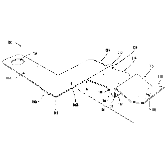
FIG. 1 is a representative drawings of a flat spring with a V-shaped
protrusion 100,
according to exemplary embodiments. The flat spring with V-shaped protrusion,
referred to
herein as a novel flat spring 100, is used in a surge protection device (SPD)
such as a thermal
metal oxide varistor (TMOV). The novel flat spring 100 consists of a first
terminal or contact
lead 102 with circular opening 104 at one end and a second terminal or solder-
side terminal 118
having a circular opening 120 at its other end, with the opening 104 being
larger than the
opening 120. The first terminal (contact lead) 102 has two portions 102a and
102b, disposed in a
3
CA 03158217 2022-5-12
WO 2021/169046
PCT/CN2020/089639
substantially L-shape to one another, with the two portions being flat
surfaces in the same plane.
Portion 102a is disposed in a first direction while portion 102b is disposed
orthogonally thereto,
with a bend or elbow 106 therebetween. Disposed at opposing sides of the
portion 102b are
sawtooth features 108a and 108b.
The next section 126 of the novel flat spring 100 is a multi-part section
consisting of
join region 124, region 114, V-shaped protrusion 110, region 116, and the
solder-side terminal
118. The multi-part section 126 is orthogonal to the second portion 102b and
is parallel to the
first portion 102a of the contact lead 102. The join region 124 is a thin,
flat portion lying flush
against the second portion 102b of the contact lead 102 and forming a bend
122. The join region
124 lies in the same plane as the contact lead 102. A small protrusion 112,
formed at the mating
point of the second portion 102b and the join region 124, is adjacent to the
second sawtooth
portion 108b. The region 114 is flush against the join region 124 but the two
regions are not
planar.
Connected between the region 114 and a region 116 is the V-shaped protrusion
110
having first side 128, bottom portion 130, and second 132. The first side 128
is connected to the
region 114 and the second side 132 is connected to the region 116. The region
116 is connected
to the solder-side terminal 118. As will be shown, the bottom portion 130 has
a first depth, and
the solder-side terminal 118 has a second depth, with the first depth being
lower than the second
depth.
The novel flat spring 100 is designed to be part of an SPD such as a TMOV,
with the
contact lead 102 being one of two terminals of the TMOV. Once the novel flat
spring 100 is part
of the SPD, the contact lead 102 is welded or soldered to the electrical
circuit/system being
4
CA 03158217 2022-5-12
WO 2021/169046
PCT/CN2020/089639
protected. Before describing the novel flat spring 100 in more detail, a prior
art flat spring is
introduced.
FIG. 2 is a representative drawings of a flat spring 200, according to the
prior art.
The prior art flat spring 200 features first and second terminals 202 and 210,
with regions 204
and 206 therebetween. The terminal 202 is orthogonal to the region 204 and
parallel to the
region 206. There is a region 208 that is not planar with the region 206. A
common problem
with the prior art flat spring 200 is that, when part of an SPD housing, an
arc shield slider of the
SPD is blocked by the flat spring during the tripping process.
As solder paste will inevitably attach to two solder sides when weldments
depart from
each other, the triggered flat spring 200 will have residual solder paste
attached in all soldered
products. Once the arc shield slider in the SPD is blocked, the arc shielding
function will not
work and the SPD is likely to experience an insulation flashover accident.
This problem may
result in the SPD or TMOV catching fire. Further, the alarm system which is
supposed to be
triggered by the arc shield slider becomes disabled.
FIGs. 3A and 3B are exploded 300A and cutaway 300B views, respectively, of an
SPD assembly including the novel flat spring 100 of FIG. 1, according to
exemplary
embodiments. Starting with the exploded view 300A, the SPD assembly includes
an inner
housing 302, two springs 304a and 304b (collectively, "springs 304"), an arc
shield 306, the
novel flat spring 100, an MOV 310, a microswitch 312, and outer housing 314.
The MOV 310,
which may be epoxy coated, includes a round electrode 316 and a contact lead
308.
The arc shield 306 is inserted into receiving slots of the inner housing 302
of the SPD
assembly, with the springs 304 disposed therebetween and creating tension
against the arc shield.
CA 03158217 2022-5-12
WO 2021/169046
PCT/CN2020/089639
The arc shield 306 and springs are arranged in the inner housing 302 to be
able to slide back and
forth. The arc shield 306 is thus the "slider" portion of the SPD assembly. As
the name implies,
the arc shield 306 is designed to move over and thus protect the MOV 310 from
an electrical arc
during an overvoltage event. During normal operation, the arc shield 306 is
inserted into the
inner housing 302 and remains flush against the springs 304. But, during an
overcurrent event,
the arc shield 306 moves to protect the MOV 310 from an electrical arc, which
would otherwise
damage or destroy the MOV.
The contact lead 308 is connected, such as by welding, to the MOV 310, with
the
contact lead 102 of the novel flat spring 100 being the other contact lead of
the MOV. Both the
contact lead 308 and the contact lead 102 (also known as terminals) will be
welded to the
electrical circuit being protected, such as to a bus bar. The novel flat
spring 100 is disposed in a
plane above the arc shield 306 with the arc shield being in a plane above the
MOV 310.
The cutaway view 300B shows the SPD assembly following an overvoltage event,
with the arc shield 306 being fully released from its initial position against
one edge (the left side)
of the SPD housing so as to be disposed over the electrode 316 of the MOV 310.
The novel flat
spring 100 is disposed in a plane over the arc shield 306, which is itself
disposed in a plane over
the MOV 310 in the housing 302. One of the two springs 304 is also visible, as
is the electrode
316 of the MOV 310. The contact lead 102 of the novel flat spring 100 and the
contact lead 308
of the MOV 310 extend outside the housing 302 and are to be welded to the
circuit/system being
protected prior to operation.
In contrast to the prior art flat spring 200 (HG. 2), the V-shaped protrusion
110 of the
novel flat spring 100 enables the arc shield 306 to maintain contact with the
novel flat spring and
6
CA 03158217 2022-5-12
WO 2021/169046
PCT/CN2020/089639
very quickly push the V-shaped protrusion of the novel flat spring during an
overvoltage event
Further, although there is contact between the V-shaped protrusion 110 and the
arc shield 306,
the V-shaped protrusion 110 of the novel flat spring 100 will not block the
arc shield sliding
operation, enabling the arc shield 306 to move as designed when the
overvoltage condition
occurs. This is true even though the novel flat spring 100 may still have some
attached solder
paste on the solder-side terminal 118.
FIGs. 4A-4C provide views 400A-400C of an SPD assembly including the novel
flat
spring 100 of FIG. 1, according to exemplary embodiments. The view 400A shows
the SPD
assembly before an overvoltage event; the view 400B shows the SPD assembly
during an
overvoltage event; and the view 400C shows the SPD assembly following an
overvoltage event.
In this view 400A, the solder-side terminal 118 of the novel flat spring 100
is
soldered to the electrode 316 of the MOV 310. During the assembly process, the
solder paste is
placed between the solder-side terminal 118 and the electrode 316 of the MOV
310. After
reflow soldering, the solder paste will turn into a solid, thus forming an
electrical connection
between the novel flat spring 100 and the electrode 316 of the MOV 310. When
an overvoltage
condition occurs, the solder will melt due to overheating caused by the
overvoltage, thus
breaking the connection between the novel flat spring 100 and the electrode
316.
In the view 400A, the V-shaped protrusion 110 of the novel flat spring 100 is
"in
front of' or "to the right of' the arc shield 306, with the arc shield being
to the left side of the
assembly. Thus, the arc shield 306 is not disposed directly over or above the
electrode 316 of the
MOV 310. By contrast, the view 300B of FIG. 3B shows the arc shield 306
directly over the
7
CA 03158217 2022-5-12
WO 2021/169046
PCT/CN2020/089639
electrode 316 of the MOV 310, with the V-shaped protrusion 110 being above the
arc shield.
The view 300B thus shows the SPD assembly during an overvoltage event.
In the view 400B, the solder-side terminal 118 is no longer connected to the
electrode
316 of the MOV 310. Thus, an open circuit is formed and the MOV is thus
protected from
catching fire during the overvoltage event. This is because the solder has
melted during the
overvoltage event, separating the novel flat spring 100 from the electrode
316. Once the solder-
side terminal 118 is no longer coupled to the electrode 316, the springs 304
of the arc shield 306
push the arc shield over the electrode 316 (in a leftward direction in the
view 4008), with the arc
shield pushing the V-shaped protrusion 110, which further pushes the solder-
side terminal
upward.
In some embodiments, the soldering material used to electrically connect the
solder-
side terminal 118 to the electrode 316 of the MOV 310 has a low melting point,
relative to the
other components of the SPD assembly. Thus, the solder will melt before an
electrical arc is able
to catch the MOV on fire. In one embodiment, the solder material is Sn4213158
with a melting
point of 138 degrees Celsius. In another embodiment, the solder material is
Sn99.3Cu0.7, with a
melting point of 217 degrees Celsius. In another embodiment, the solder
material is
SnAG3.0Cu0.5 with a melting point of 217 degrees Celsius. Other soldering
materials may be
used as well, as long as the melting point is set so that the solder melts
first, before other
materials of the SPD assembly.
In the side cutaway view 400C, the arc shield 306 has been fully engaged
following
an overvoltage event, so as to be disposed above the electrode 316 of the MOV
310. The V-
shaped protrusion of the novel flat spring 100 is above the arc shield 306 and
does not impede its
8
CA 03158217 2022-5-12
WO 2021/169046
PCT/CN2020/089639
movement, in this view, leftward over the MOV 310. FIG. 3B also shows the
position of the arc
shield over the electrode 316 of the MOV 310 following an overvoltage event.
Returning to FIG. 4A, in the view 400A before the overvoltage event occurs,
the V-
shaped protrusion 110 is disposed between the solder-side terminal 118 of the
novel flat spring
100 and the arc shield 306. The depth of the V-shaped protrusion 110 is lower
than the solder-
side terminal 118 so that the sliding action of the arc shield 306 can avoid
getting blocked by
residual solder paste attached on the face of the electrode 316. Because the
solder-side terminal
118 of the novel flat spring 100 is higher than the bottom surface of the V-
shaped protrusion, this
ensures that the arc shield 306 will not be blocked in the tripping process.
The sawtooth features 108 and the protrusion 112 introduced in FIG. 1 of the
novel
flat spring 100 are shown in the exploded view 300A (FIG. 3A). The sawtooth
features 108 are
at both edges of the portion 102b of the novel flat spring 100 (FIG. 1) and
provide reliability
during mechanical movement of the flat spring. The sawtooth features 108 and
the protrusion
112 facilitate attachment of the novel flat spring 100 into the inner housing
302 of the SPD
assembly 300. The inner housing 302 includes respective receiving
edges/openings (not shown)
to ensure that the novel flat spring 100, once attached into the housing,
remains fixably in place.
The sawtooth edges 108 and protrusion 112 thus provide additional reliability
in the complex
environment of the SPD assembly.
In some embodiments, the minimum gap between the solder-side terminal 118 of
the
novel flat spring 100 and the arc shield 306 is 0.2 min or more. In an
exemplary embodiment,
the minimum gap between the solder-side terminal 118 and the arc shield 306 is
1.49 nun. This
9
CA 03158217 2022-5-12
WO 2021/169046
PCT/CN2020/089639
space ensures that the arc shield 306 will not be blocked by residual
soldering material in the
tripping process.
FIG. 5 shows another view 500 of an SPD assembly including the novel flat
spring
100 of FIG. 1, according to exemplary embodiments. The first terminal or
contact lead 102 that
is part of the novel flat spring 100 and the second terminal or contact lead
308 that is welded to
the MOV 310 (FIG. 3A) are shown extending to the right of the outer housing
314. The arc
shield 306 is disposed in a plane above the MOV 310 while the novel flat
spring 100 is disposed
in a plane above the arc shield. The microswitch 316 is also visible on the
left side of the
housing 314. The solder-side terminal 118 of the novel flat spring 100 is
disposed over the
electrode 316 of the MOV 310. In this view 500, an overvoltage event has
commenced, and the
solder has melted such that the solder-side tertninal 118 is no longer
electrically coupled to the
electrode 316 of the MOV 310. The arc shield 306 has partially moved over the
electrode it is
designed to protect.
FIGs. 6A ¨ 6C are technical drawings of the novel flat spring 100, according
to
exemplary embodiments. The measurements are given in millimeters (mm). For
example, HG.
6A shows that the width of the first terminal or contact lead 102 is 7.11 mm
and the width of the
second solder-side terminal 118 is 9.25 mm, which is the same width as the
multi-part section
126 of the novel flat spring 100. Further, in some embodiments, the length of
the second solder-
side terminal 118 is between 3.0 mm and 3.8 mm. In an exemplary embodiment,
the length of
the second solder-side terminal is 3.41 nun. FIGs. 6B and 6C show the relative
angular
disposition of the region 114, the V-shaped protrusion 110, the region 116,
and the solder-side
terminal 118. Because the solder-side terminal is higher than the bottom
surface of the V-shaped
protrusion, this ensures that the arc shield will not be blocked in the
tripping process. In the
CA 03158217 2022-5-12
WO 2021/169046
PCT/CN2020/089639
novel flat spring 100, the solder area is neither too small to provide
mechanical strength nor too
big to trip fast enough to protect the MOV disk 310 from catching fire.
Thus, the novel flat spring 100 with the V-shaped protrusion 110 can address
the
serious problems of prior art SPDs catching fire with high reliability. The V-
shaped protrusion
110 is in front of solder area of the novel flat spring 100. The depth of the
V-shaped protrusion
110 is lower than the solder-side terminal so that the arc shield slider can
avoid getting blocked
by residual solder paste attached on the face of the weld.
The novel flat spring 100 is applicable to all kinds of solder paste and
solder methods.
The solder area is so precise that the novel flat spring 100 provides
mechanical strength and
tripping sensitivity at the same time. The V-shaped protrusion feature solves
a common issue
that the slider of the SPD is blocked in the tripping process. The novel flat
spring 100 is easy to
manufacture at a low cost and can be used with a variety of SPD modules,
including TMOV
devices.
Thus, in an exemplary embodiment, when an overvoltage event occurs, the
following
operations will occur. First, the solder between the solder-side terminal 118
and the electrode
316 will melt. Next, the two coil springs 304a and 304b (FIG. 3A) will push
the arc shield 306
to move and push the V-shaped protrusion 110 of the novel flat spring 100. In
turn, this will
cause the solder-side terminal 118 to move upward, thus causing an open
circuit. The V-shaped
protrusion of the novel flat spring 100 thus provides mechanical strength to
force the open circuit.
The novel flat spring 100 also enhances/improves the tripping sensitivity of
the SPD module,
which protects the valuable MOV inside.
11
CA 03158217 2022-5-12
WO 2021/169046
PCT/CN2020/089639
In exemplary embodiments, the SPDs described herein with the novel flat spring
100
are useable in an MOV with an ultra-fast activation thermal fuse. No
additional overcurrent fuse
is needed, with the SPD satisfying UL 1449 Type 1 and 2 applications. The SPD
with the novel
flat spring 100 further is able to safely and quickly form an open circuit
covering a very wide
range. In some embodiments, the range is from 0.125A - 200kA, which is
suitable to protect a
variety of different kinds of circuits.
As used herein, an element or step recited in the singular and proceeded with
the
word "a" or "an" should be understood as not excluding plural elements or
steps, unless such
exclusion is explicitly recited. Furthermore, references to "one embodiment"
of the present
disclosure are not intended to be interpreted as excluding the existence of
additional
embodiments that also incorporate the recited features.
While the present disclosure makes reference to certain embodiments, numerous
modifications, alterations and changes to the described embodiments are
possible without
departing from the sphere and scope of the present disclosure, as defined in
the appended
claim(s). Accordingly, it is intended that the present disclosure not be
limited to the described
embodiments, but that it has the full scope defined by the language of the
following claims, and
equivalents thereof.
12
CA 03158217 2022-5-12