Note: Descriptions are shown in the official language in which they were submitted.
CA 03158345 2022-04-14
WO 2021/075999 PCT/RU2019/000749
1
ELECTROCHROMIC DEVICES, METHODS OF MANUFACTURING AND
OPERATION THEREOF
TECHNICAL FIELD
[0001] The present invention relates to electrochromic materials, devices,
methods of their
manufacturing and methods of their operation.
BACKGROUND
[0002] Electrochromism is the physical phenomenon found in certain compounds,
compositions or
assemblies which can reversibly change optical properties such as color or
light transmittance due to
electric current arising with an application of a voltage called a control
voltage. Electrochromism
provides the basis for operation of various electrochromic devices, such as
smart glass in the form of
windows, mirrors and displays. Various types of optical materials and
structures can be used to construct
compositions with electrochromic properties, with the specific structures
being dependent on the
specific purpose of the electrochromic device.
[0003] A variety of patents and patent applications disclose electrochromic
materials and devices. Such
patents and patent applications include, for example, US 2015/0353819
describes electrochromic
compositions and devices; RU2642558C1 describes manufacturing and operation of
organic
electrochromic devices manufactured by UV-curing of polymer matrices
containing organic active
electrochromic materials; US 6262832, US 6433914, US 6445486, US 6710906, US
7031043 and US
8294974 disclose various electrochromic materials and devices. A review
article discloses all-in-one
gel-based electrochromic devices. See Alesanco et al., Materials 2018, 11,414,
pp. 1-27.
[0004] However, there is a continuing need for electrochromic materials,
devices, methods of their
manufacturing and methods of their operation.
SUMMARY OF THE DISCLOSURE
[0005] Advantages of the present disclosure include electrochromic devices and
components thereof
and systems and methods for controlling electrochromic devices. Additional
advantages of the present
disclosure include electrochromic materials, electrochromic compositions and
electrochromic layers. In
certain aspects of the present disclosure, the electrochromic composition and
layers can be in the form
of a gel. The present disclosure also provides methods to fabricate
electrochromic devices and
components thereof, electrochromic compositions, layers and gels.
[0006] Additional advantages of the present invention will become readily
apparent to those skilled in
this art from the following detailed description, wherein only the preferred
embodiment of the invention
is shown and described, simply by way of illustration of the best mode
contemplated of carrying out the
CA 03158345 2022-04-14
WO 2021/075999
PCT/RU2019/000749
2
invention. As will be realized, the invention is capable of other and
different embodiments, and its
several details are capable of modifications in various obvious respects, all
without departing from the
invention. Accordingly, the drawings and description are to be regarded as
illustrative in nature, and not
as restrictive.
BRIEF DESCRIPTION OF THE DRAWINGS
[0007] Reference is made to the attached drawings, wherein elements having the
same reference
numeral designations represent similar elements throughout and wherein:
[0008] Fig. lA illustrates an electrochromic device in accordance with an
implementation of the present
disclosure.
[0009] Fig. 1B illustrates an example of the structure of the variable
transmittance layer of an
electrochromic device in accordance with an implementation of the present
disclosure.
[0010] Fig. 1C illustrates exemplary viologens that can be used in practicing
aspects of the present
disclosure.
[0011] FIG. 2 illustrates designs for several electrochromic devices according
to aspects of the present
disclosure.
[0012] FIG. 3 illustrates a process for providing bus bars over an edge of a
substrate which provide
electrical contacts to electrodes of an electrochromic device in accordance
with an embodiment of the
present disclosure.
[0013] FIG. 4 illustrates an alternate example of an electrode having a bus
bar for an electrochromic
device in accordance with an embodiment of the present disclosure.
[0014] FIG. 5A illustrates a seal arrangement for sealing electrochromic
composition (ECC) in an
electrochromic device in accordance with an embodiment of the present
disclosure.
[0015] FIG. 5B illustrates an alternative seal arrangement for sealing the
electrochromic composition
(ECC) in an electrochromic device in accordance with an embodiment of the
present disclosure.
[0016] FIGs. 6A and 6B illustrate a method of assembling an EC device in
accordance with an
embodiment of the present disclosure.
[0017] FIG. 7A illustrates a method of pouring an ECC on to a substrate in
manufacturing an EC device
in accordance with an embodiment of the present disclosure.
[0018] FIG. 7B illustrates an alternate method of pouring the ECC on to a
substrate while manufacturing
an EC device in accordance with an embodiment of the present disclosure.
[0019] FIG. 8 illustrates a further alternate method of pouring the ECC on to
a substrate while
manufacturing an EC device in accordance with an embodiment of the present
disclosure.
CA 03158345 2022-04-14
WO 2021/075999
PCT/RU2019/000749
3
[0020] FIG. 9 illustrates a method of providing an ECC on to an electrodic
film in accordance with an
embodiment of the present disclosure.
[0021] FIG. 10A and FIG. 10B illustrate configurations of a variable
transmittance layer used for an EC
device in accordance with an embodiment of the present disclosure.
[0022] FIG. 10C illustrates an electrochromic layer having a center area with
a higher conductivity than
a peripheral area of the layer
[0023] FIG. 11 is a flow chart depicting a control algorithm for controlling
an EC device in accordance
with an embodiment of the present disclosure.
[0024] FIGs. 12A, 12B, 12C and 12D list and show viologens that can be used in
compositions, layers,
gels and devices of the present disclosure.
DETAILED DESCRIPTION OF THE DISCLOSURE
[0025] The following naming conventions will be used throughout this
disclosure:
[0026] Chemical potential ( ) ¨ the energy that can be absorbed or released
due to a change of the
particle number of the given species, e.g. in a chemical reaction or phase
transition. The chemical
potential of a specie in a mixture is defined as the rate of change of free
energy of a thermodynamic
system with respect to the change in the number of atoms or molecules of the
specie that are added to
the system. Thus, it is the partial derivative of the free energy with respect
to the amount of the species,
aG
all other species' concentrations in the mixture remaining constant:
= . The molar
aNi
chemical potential is also known as partial molar free energy. When both
temperature and pressure are
held constant, chemical potential equals the partial molar Gibbs free energy.
In ideal mixtures or
solutions the chemical potential can be expressed as =
+ RT1nx1, where xi is the mole fraction of
the ith component and pti* is the molar free energy of the component in its
pure form at that temperature
and pressure. For non-ideal mixtures and solutions the chemical potential is =
+ RT1na1 = 14 +
RTlnyi xi, where a, is the relative activity of the it" component and 7, is
the activity coefficient.
[0027] Electrochemical potential (j.T) ¨ a thermodynamic measure of chemical
potential that does not
omit the energy contribution of electrostatics: rt, = + ziFv, where zi is the
charge of ith component,
F is the Faraday constant and is local electrostatic potential.
[0028] Concentration ¨ the abundance of a constituent divided by the total
volume of a mixture.
[0029] Activity ¨ a measure of the "effective concentration" of a specie in a
mixture, in the sense that
the species' chemical potential depends on the activity of a real solution in
the same way that it would
depend on concentration for an ideal solution. The absolute activity of a
substance is denoted by A =
exp õo
/RT), and the relative activity is defined as a = expe
60,), where 1.t is chemical potential
CA 03158345 2022-04-14
WO 2021/075999 PCT/RU2019/000749
4
12 is the molar free energy of the material in some defined standard state for
which the activity is taken
as unity (standard chemical potential).
[0030] Rate-limiting process (step) ¨ the slowest process of a consecutive
reaction in means of the least
rate coefficient.
[0031] Redox couple ¨ a pair of molecules (ions) which differ in one or more
electrons.
[0032] Redox reaction ¨ a chemical reaction in which the reactants exchange
electrons between each
other. The processes of gaining and expelling electrons are termed reduction
and oxidation, respectively.
Each redox reaction comprises both reduction and oxidation occurring
simultaneously. The reactants
undergoing reduction are termed oxidant, whereas those being oxidized are
termed reductant. The redox
reaction can be formally split into, at least, two half-reactions representing
separately the oxidation and
reduction. The oxidized and reduced forms of a single participant in a half-
reaction comprise a redox
couple. Each half-reaction is attributed with a standard (redox) potential,
measured versus the standard
hydrogen electrode as a reference system.
[0033] Reversible redox reaction ¨ the term is used in three different
contexts: Chemically reversible
redox reaction ¨ a redox reaction that can proceed in two directions, i.e.
from reactants to products and
in reverse direction. Thermodynamically reversible redox reaction ¨ a redox
reaction that is at the
equilibrium at every moment. From the initial to the final state, it proceeds
through a series of
equilibrium states, thus proceeding infinitesimally slow and requiring an
infinite length of time. An
infinitesimal change in the direction of the driving force causes the
direction of the process to reverse.
Electrochemically reversible redox reaction ¨ a redox reaction or the
electrode reaction for which the
surface concentrations of both species of the redox couple obey the Nernst
equation at any potential
difference applied at the electrode-electrolyte interface. In this case the
charge transfer at the interface
is much faster than all coupled mass transport processes.
[0034] Interface ¨ the two-dimensional plane separating two phases. The
general thermodynamic
requirement for the stability of an interface between two phases is a positive
Gibbs energy of formation,
because otherwise the interface would either fluctuate or disappear. Since the
molecular forces on either
side of an interface possess a specific anisotropy the structure of the utmost
surface layers differs from
that inside the phases.
[0035] Electroactive substance ¨ a substance that undergoes a change of
oxidation state during an
interphase charge transfer upon application of an electric field between the
phases.
[0036] Electrode (Engineering/Electronics) ¨ an element made of an electronic
conductor through which
electrical current enters or leaves an object or region. In the simplest case
a pure solid metal; however,
the electronic conductor may be also an alloy (e.g., an amalgam), carbon
(e.g., graphite, glassy carbon,
carbon nanotubes), a semiconductor (e.g., boron-doped diamond, a metal oxide,
metal salt, doped
CA 03158345 2022-04-14
WO 2021/075999
PCT/RU2019/000749
silicon, germanium alloys) or any other material which conducts electrical
current by the drift of free
electrons.
[0037] Optically transparent electrode (OTE) ¨ an electrode (engineering) that
is transparent to visible
light. OTEs can include thin films of metals or semiconductors deposited on
transparent substrate (glass,
quartz, plastic, etc.). Further, OTEs can be made from transparent oxides,
commonly called Transparent
Conductive Oxides (TCO). Alternatively, OTEs can be in a form of fine wire
meshes or grids. OTEs
can act as electric current distribution manifolds, bringing current to and
from every area of an EC layer
(ECL), for example. Ideally, OTEs do not substantially distort (absorb and
scatter) transmitted light.
[0038] Ideally polarizable electrode ¨ an electrode, whose electronic and
ionic conductor phases does
not possess a common component capable of changing its charge and being
transferred between phases
and therefore not able to reach a thermodynamic equilibrium. The criterion is
applicable only under a
number of conditions: potential ranges, time scales, etc.
[0039] Ideally nonpolarizable electrode ¨ an electrode having unhindered
exchange of common charged
particles between its electronic and ionic conductor phases. The criterion is
applicable only under a
number of conditions: potential ranges, time scales, etc.
[0040] Electrocatalytic electrode ¨ an electrode at which an electrochemical
process is subject to
catalysis, i.e. in most cases its rate is increased.
[0041] Reference electrode ¨ an electrode of an electrochemical cell which
potential is chosen as the
zero value of the electric potential scale. In a three-electrode cell with
aqueous electrolyte is usually
represented by a separate electrode of 2'd kind (e.g., saturated calomel
electrode, SCE or AgC1 electrode)
due to their potential remaining practically constant during an experiment. In
non-aqueous (organic)
systems pseudo-reference (e.g. Ag metal) electrodes are commonly used with an
in situ redox reference,
which redox potential is practically independent of the electrolyte properties
(e.g., ferrocene). The
principle of the three-electrode cell assumes that the current flowing through
the reference electrode is
close to zero. In a 2-electrode cell the counter electrode is used as a
reference electrode.
[0042] Standard hydrogen electrode ¨ the primary standard of electrochemistry,
an electrode, the
standard potential of which is defined as the value of the standard potential
of a cell reaction that involves
the oxidation of molecular hydrogen to solvated (hydrated) protons.
[0043] Working electrode ¨ an electrode at which a given electrode process is
examined. This term is
usually used in context of analytical electrochemistry.
[0044] Counter electrode ¨ an electrode that represent a second electrolyte-
electrode interface in a cell
having a working electrode and thus allowing to connect the cell to an
external circuit and allowing the
processes of the working electrode to proceed.
CA 03158345 2022-04-14
WO 2021/075999 PCT/RU2019/000749
6
[0045] Cathode ¨ in an electrochemical cell, a cathode is the electrode where
reduction occurs and
electrons flow from electrode to electrolyte.
[0046] Anode ¨ in an electrochemical cell, an anode is the electrode where
oxidation occurs and
electrons flow from electrolyte to electrode.
[0047] Anodic/cathodic/electrodic stack ¨ a stack of layers including at least
one anode layer or at least
one cathode layer. Such a stack can carry the functions of mechanical support
(substrate), surface
electronic conductivity and interfacial charge transfer. Interlayer adhesion
between a substrate and a
surface conductor may be promoted by additional layer(s) if needed. An anodic
stack acts as anode at
charging conditions, a cathodic stack acts as cathode at charging conditions
(and vice versa at
discharging). The functions of the layers may be combined, i.e. one layer may
carry several functions.
Similarly, one function may be carried by several layers.
[0048] Electrochemical cell ¨ A combination of at least two electrodes in
contact with an ionic
conductor (solution, in common case). An electrochemical cell may operate as a
galvanic cell if the
reactions occur spontaneously and chemical energy is converted into electrical
energy or as an
electrolysis (or electrolytic) cell in which electrical energy is converted
into chemical energy.
[0049] Galvanic cell ¨ an electrochemical cell in which reactions occur
spontaneously at the electrodes
when they are connected externally by a conductor. It means that the reaction
occurring must have
negative Gibbs energy difference (AG <0).
[0050] Electrolysis cell (electrolytic cell) ¨ an electrochemical cell, the
Gibbs reaction of which is
positive (AG > 0) and hence no reaction occurs until the cell is externally
supplied with electrical energy.
[0051] Charge/discharge of an electrochemical cell ¨ the process that is
accompanied by flow of electric
current, which causes the equilibrium potential difference between cathode and
anode to
increase/decrease. At charge an electrochemical cell is working as an
electrolytic cell and at discharge
it is working as a galvanic cell.
[0052] Cell reaction ¨ a chemical reaction occurring spontaneously in a
galvanic cell. The Gibbs energy
change of the reaction is converted into electrical energy and heat.
[0053] Half-reactions (electrode reactions) ¨ chemical processes (oxidation or
reduction) taking place
spatially separated at the electrodes in such a way that they are
interconnected by the ion transport
through the ionic conductor separating two electrodes.
[0054] Open-circuit potential (OCP) ¨ in general, a voltage that is measured
between a couple of
electrodes of a system when no potential or current is being applied. For an
electrochemical cell, the
potential of the working electrode relative to the reference electrode when no
potential or current is
being applied to the cell. In case of a reversible electrode system is also
referred to as the equilibrium
CA 03158345 2022-04-14
WO 2021/075999
PCT/RU2019/000749
7
potential. Otherwise it is called the rest potential or the corrosion
potential, depending on the studied
system.
[0055] Equilibrium electrode potential - the value of electrode potential
determined exclusively by a
single redox system Ox/Red in the absence of current under complete
equilibration. The rates of Ox to
Red reduction and of Red to Ox oxidation are equal under these circumstances.
The value of equilibrium
electrode potential is determined by the Nernst equation.
[0056] Exchange current density - at an equilibrated electrode, where the net
current value equals zero,
a value that corresponds to the magnitude of the anodic current density
component balanced with the
cathodic one.
[0057] Nernst equation - a fundamental equation in electrochemistry that
describes the dependence of
the equilibrium electrode potential on the composition of contacting phases:
Eceti = AG inF = E -
(RT / ) v
nFJ vi lnai, where a, are activities of the species involved.
[0058] Charge transfer coefficient (a) - a coefficient that gives the ratio of
the change of the height of
the energy barrier the electron has to surmount during charge transfer with
respect to the change of
electrode potential E. A value of a = 0 implies no influence of the electrode
potential change on the
barrier height, a = 1 implies that the change of electrode potential causes an
exactly equal change of
barrier height. The symmetrical energy barrier results in a = 0.5. Typically,
a is in the range of 0.3 to
0.7.
[0059] Butler-Volmer equation - the fundamental equation of electrode kinetics
that describes the
aFn
relationship between the current density and the electrode potential: j = Jo [
a x exp (- ¨RT
a0x initial
aRed exp)1, where j is the current density, ai are the activities at the
interface, a is the charge
aRed initial RT
transfer coefficient, F is the Faraday constant, 1 = (E - Eformai) is the
overpotential and jo is the exchange
current density.
[0060] Frumkin effect - originating from the Frumkin's theory of slow
discharge, the effect of deviation
of driving potential value form the overpotential arising from the
electroneutrality breaking. The
Frumkin correction contributes to the Butler-Volmer equation: j = jo "x
exp aF(?i-ipi))
a0x initial
RT
aRed exp((1-a)F(n-lP15], where in (psi-prime potential) stands for the
potential in the point of
aRed initial RT
reactant location relative to the bulk liquid potential. Outer Helmholtz plane
potential ((pow) is often
considered as the psi-prime potential since OHP is the position of the most
probable interfacial charge
transfer.
[0061] Standard potential - the equilibrium potential of an electrode under
standard-state conditions,
i.e., in solutions with the relative activities of all components being unity
and a pressure being 1 atm
CA 03158345 2022-04-14
WO 2021/075999 PCT/RU2019/000749
8
(ignoring the deviations of fugacity and activity from pressure and
concentration, respectively) at
temperature T.
[0062] Formal potential (Ef) ¨ the value that replaces the standard potential
of a cell reaction when the
values of activity coefficients are unknown and therefore concentrations used
in the equation expressing
the composition dependence of cell potential instead of activities.
[0063] Half-wave potential (E1/2) ¨ the potential corresponding to a half of
the limiting current for
various wave-shaped electrochemical responses. For a reversible polarographic
wave and a solution
containing both the oxidized (0x) and the reduced (Red) species, Ein deviates
from the formal potential:
RTin YOx1150;
E112 = Ef ¨nF(v [---n ).
Redv ¨Red
[0064] Onset potential (Eonset) ¨ in electrochemistry, an ill-defined
potential at which a specific process
starts as determined by an increase in current in a current-potential curve.
[0065] Zeta potential () ¨ the electrical potential difference between the
bulk solution and the "shear
plane/slippery plane" or outer limit of the rigid part of the double layer,
often represented by OHP.
[0066] Overpotential ¨ a deviation of the potential of an electrode from its
equilibrium value required
to cause a given current to flow through the electrode.
[0067] Electrode charge ¨ the total quantity of electricity required to charge
the interface up to its
equilibrium state at certain potential conditions of no charge exchange
between the electronic conductor
surface and electrolyte bulk.
[0068] Potential of zero charge (Epze) ¨ the potential corresponding to zero
electrode charge.
[0069] Redox potential ¨ the equilibrium potential of a redox couple as given
by the Nernst equation.
[0070] Band bending ¨ the consequence of the occurrence of internal electric
fields inside
semiconductor materials that makes the band edges to appear curved on the
energy band diagram of an
interface with the semiconductor.
[0071] Flat-band potential ¨ in an energy barrier formed for example at metal-
semiconductor junctions,
metal¨insulator¨semiconductor junctions and solution¨semiconductor interfaces,
a potential at which
the electric field equals zero at the semiconductor interface, i.e., there is
no band bending. In case of
solution¨semiconductor interfaces, the flat-band potential corresponds to the
condition of absence of
excess charge and consequently, depletion layer, in the semiconductor.
[0072] Applied potential ¨ An electrical potential difference applied
externally to a material, device,
cell, interface, etc. Being applied to an electrochemical cell, the applied
potential is divided into two
electrode potentials, each of which is the difference of potential existing
between the bulk of the solution
(e.g., an EC layer) and the interior of the conducting material of the
electrode, an ohmic potential drop
through the solution (e.g., the EC layer), and another ohmic potential drop
through each electrode. In
the context of an electrochromic device, the applied potential can manifest
itself as a combination of (1)
CA 03158345 2022-04-14
WO 2021/075999
PCT/RU2019/000749
9
anodic ohmic potential drop, through the electrode from anode's conductive
lead to a specific point on
the anodic electrode, (2) potential drop from this specific point of the
anodic electrode, across the
conductive interface between anode and EC layer, to the corresponding point of
EC layer which is in
immediate proximity to this specific point on the anode; (3) cathodic ohmic
potential drop, through the
electrode from cathode's conductive lead to a specific point on the cathodic
electrode, (4) potential drop
from this specific point of the cathodic electrode, across the conductive
interface between cathode and
EC layer, to the corresponding point of EC layer which is in immediate
proximity to this specific point
on the cathode; and (5) potential drop between same anodic and cathodic points
of the EC layer.
[0073] Electrochemical window ¨ in electrochemical experiments, the range of
potentials that is
accessible without appreciable current flow, i.e., the potential range in
which the electrodes may be
considered as ideally polarizable.
[0074] Bandgap, Eg ¨ an energy difference between the bottom of the conduction
band and the top of
the valence band in a semiconductor or an insulator. "Wide bandgap" stands for
bandgaps >3.0 eV, and
"narrow bandgap" indicates values <2.0 eV.
[0075] Conduction band ¨ vacant or only partially occupied set of many closely
spaced electronic levels
resulting from an array of a large number of atoms forming a system in which
the electrons can move
freely or nearly so.
[0076] Valence band ¨ highest energy continuum of energy levels in a solid
that is fully occupied by
electrons at 0 K.
[0077] Fermi energy (EF) ¨ the energy difference between the highest and
lowest occupied single-
particle states in a quantum system of non-interacting fermions at absolute
zero temperature. In context
of the band theory is referring to the energy of a level (which is called a
Fermi level) that is occupied by
an electron with half probability. The Fermi level is virtual and may not be
really existing (e.g. being
located within the bandgap of a semiconductor or insulator). EF of a solution
(EF, redox) is the energy at
which the probability of electron detection at the electrolyte side of an
interface is 0.5. This level is also
virtual and is not represented by a physically existing energy state. EF is
equal to the electrochemical
potential of electrons.
[0078] Work function ¨ the energy required to remove an electron from the bulk
of a phase to a point
well outside it. It can be expressed as Om = - EF, where EF is the Fermi
energy and E. is the electron
energy at rest at infinite distance.
[0079] Steady state (Electrochemistry) ¨ a state of a system that occurs when
a variable of interest (e.g.,
a concentration, a flux, a current, or a potential) does not change with time.
A steady state is attained
after a passage of time and theoretically requires an infinite length of time
because steady states are
CA 03158345 2022-04-14
WO 2021/075999
PCT/RU2019/000749
approached gradually rather than being obtained at a specific instant. Thus
"reaching a steady state" can
mean coming to within some specified percentage of the steady state.
[0080] Solvent - is a substance that dissolves a solute (a chemically distinct
liquid, solid or gas),
resulting in a solution.
[0081] Solvation sheath (shell) - the solvent interface of any chemical
compound that constitutes the
solute.
[0082] Reorganization energy (X) - in the Marcus theory, the change of energy
of a system resulting
from changes in bond lengths in the reacting molecules (inner component, Xi),
and changes in the radii
of solvated ions or in the solvation sphere including orientation of the
solvent dipoles (outer component,
Xo).
[0083] Debye length (0) - a measure of a charge carrier's net electrostatic
effect in a solution and how
far its electrostatic effect persists: ic-1 - 68 kBT for a solution, where
is the relative permeability, a
e2
is the electric constant, e is the electron charge, kB is the Boltzmann
constant, T is absolute temperature,
C , is the concentration of ith component and z, is the charge of ith
component.
[0084] Electrolytes - compounds that dissociate into ions upon dissociation in
a solvent and which
provide by such dissociation ionic conductivity. Ionically conductive
solutions of electrolytes are also
sometimes referred to as electrolytes. Compounds that possess in the solid
state a rather high ionic
conductivity are called solid electrolytes.
[0085] Supporting Electrolyte - an electrolyte, the ions of which are not
electroactive in the range of
applied potentials being used. Typically, concentrations of supporting
electrolytes are higher than
concentrations of electroactive substances dissolved in the solution.
[0086] Electron transfer - the process by which an electron is transported
into (or out of) an otherwise
closed system, thereby inducing a change in the occupation number of at least
one electronic state.
[0087] Charge transfer reaction - an interfacial (heterogeneous) reaction that
necessarily involves a
charge transfer step. The latter can be a neutralization or formation of ions
(ion transfer), or alteration
of the ionic charge by the gain or loss electrons from or to the metal,
respectively.
[0088] Double layer - in general, a layer of charges that exists at the
interface between two conducting
media: one side carries a positive excess charge, which is balanced by a
negative excess of equal
magnitude on the other side. The resulting potential drop across the interface
is the double-layer
potential. Two limiting cases exist: at an ideally polarizable interface the
two adjacent phases cannot
exchange charges; the system then behaves like a capacitor, which can be
charged by applying an
external potential. At an ideally nonpolarizable interface the two phases can
exchange charge carriers,
CA 03158345 2022-04-14
WO 2021/075999 PCT/RU2019/000749
11
ions or electrons, and in the stationary case the potential difference is
determined by the difference of
the chemical potential of these carriers in the two phases.
[0089] Inner Helmholtz layer ¨ in a double layer, a layer that comprises all
species that are specifically
adsorbed on the electrode surface. If only one type of molecule or ion is
adsorbed, and they all sit in
equivalent positions, then their centers define the inner Helmholtz plane
(IHP).
[0090] Outer Helmholtz layer ¨ in a double layer, a layer that comprises the
ions that are closest to the
electrode surface but are not specifically adsorbed. They have kept their
solvation spheres intact and are
bound only by electrostatic forces. If all these ions are equivalent, their
centers define the outer
Helmholtz plane (OHP).
[0091] Slippery plane (shear plane) ¨ an imaginary plane in a double layer
structure that separates areas
of immobilized and non-immobilized solution species.
[0092] Electrochemical impedance spectroscopy (EIS) ¨ experimental technique
based on the
measurement (under equilibrium or steady-state conditions) of the complex
impedance Z of the
electrochemical system under study as a function of the frequency, f, or
angular frequency, co, of an
imposed sinusoidal perturbation of small amplitude.
[0093] Equivalent circuit ¨ in electrochemical impedance spectroscopy (EIS), a
virtual network of ideal
passive electrical components that mimics the full electrical (AC+DC) behavior
of an electrochemical
system.
[0094] Mass transport (mass transfer) ¨ the net movement of mass from one
location, usually meaning
stream, phase, fraction or component, to another.
[0095] Diffusion ¨ the transport of particles caused by the local difference
in the chemical potential.
The flux of particles is proportional to the gradient of the chemical
potential (or concentration, in
simplified case).
[0096] Convection ¨ one of the modes of mass transport. Contrary to diffusion
or migration when
transport of the species occurs from one location in solution to another by a
molecular mechanism, in
the case of convection the movement of whole volume elements of solution takes
place. Convection
may occur due to density gradients (natural convection). A density gradient
may arise at high currents
due to the production or depletion of matter, especially in technical
electrolysis and in coulometric
experiments. Heating or cooling may also cause density gradients. Forced
convection may be
unintentional, e.g., due to the vibration, but may be induced by stirring,
etc.
[0097] Migration ¨ A kind of charge/mass transport that is related to ions and
the existence of potential
gradient in the solution. When current flows through a solution it is carried
by ions and this constitutes
the migrational transport.
CA 03158345 2022-04-14
WO 2021/075999
PCT/RU2019/000749
12
[0098] Beer-Lambert-Bouguer Law ¨ a physical law that relates the attenuation
of light to the properties
of the material through which the light is travelling. According to the Beer-
Lambert-Bouguer law, the
factor of attenuation (named optical density, D) of a beam of collimated
monochromatic radiation in a
homogeneous isotropic medium is proportional to the absorption path 1,
chemical compound's decadic
molar attenuation coefficient 6 (which includes the effects of absorption,
scattering and fluorescence)
and molar concentration C: D = ¨ lg /0= EC/, where /relates to the intensity
of passed light and Jo ¨
to the intensity of the light entering the attenuating medium. For the
solutions, the molar absorption
coefficients are used to describe the intensity of light attenuation by the
solutes.
[0099] Electrochromism (EC) is the physical phenomenon found in certain
compounds, compositions
or assemblies which can reversibly change optical properties such as color or
light transmittance due to
electric current arising with an application of a voltage called a control
voltage. Systems or materials
showing the phenomenon of electrochromism are called "Electrochromic".
[0100] Electrochromic material ¨ a material that displays electrochromism.
Such materials can be
generally classified as type I, II or III. A "type I" material is soluble in
both the reduced and oxidized
(redox) states, an example being 1,10-di-methyl-4,40-bipyridylium
("methylviologen"), which, on
reduction, switches from the colorless di-cation to the blue radical cation. A
"Type II" material is soluble
in one redox state but form a solid film on the surface of an electrode
following electron transfer. An
example here is 1,1-di-hepty1-4,4-bipyridylium ("heptyl viologen"). In "type
III" materials, such as
tungsten oxide, Prussian blue, and electroactive conjugated polymers, both or
all redox states are solids,
and such systems are generally used as thin films on electrode surfaces. For
types II and III, once the
redox state has been switched, no further charge injection is needed to retain
the new electrochromic
state and such systems are said to have "optical memory". For type I
electrochromic materials, diffusion
of the soluble electrochemically generated product material away from the
electrode occurs and it is
necessary to keep current flowing until the whole solution has been
electrolyzed. Where more than two
redox states are electrochemically accessible in a given electrolyte solution,
the electrochromic material
may exhibit several colors and be termed polyelectrochromic, a frequent
property of thin films of
electroactive conjugated polymers.
[0101] Electrochromic device (EC device) ¨ a device that uses the phenomenon
of electrochromism.
[0102] All-in-one EC devices ¨ a class of electrochromic devices where all the
electrochromic
material(s) are incorporated within ionic conductor phase(s) rather than being
set apart into separate
electrochromic phases having electronic conductivity.
[0103] Electrochromic layer (EC layer) ¨ electrochromic material or
composition that covers a surface
or is disposed between two objects. An EC layer in an all-in-one EC device
serves as an ion conducting
element which can vary optical properties of an all-in-one EC device upon
application of an electric
CA 03158345 2022-04-14
WO 2021/075999
PCT/RU2019/000749
13
input signal via electrodes of such a device. In certain aspects, an EC layer
can be substantially or
entirely clear, non-turbid, non-hazy, colorless or a colored medium. It can be
in contact with both anodic
and cathodic stacks of a variable transmittance layer or in contact with at
least one anodic or cathodic
stack and at least one auxiliary electrode (e.g., an electrode located outside
an optical path of an EC
layer) of the opposite function.
[0104] Light-absorbing compounds ¨ compounds that provide the attenuation of
the electromagnetic
radiation flux in visible and/or UV and/or NIR regions, thus (1) creating the
desired visual sensation for
a human looking through an EC device and/or for an area where it is installed
and (2) providing the EC
device the ability of regulation of the amount of the incoming electromagnetic
radiation energy in
aforementioned regions of electromagnetic radiation. These compounds are
formed and consumed
within an EC layer during normal operation of an EC device and their amounts
are varied by electric
input signals applied to the EC device.
[0105] Auxiliary compounds ¨ components that can be included in an EC
composition or layer that
facilitate reaction sequences that lead from initial electrochemical processes
to formation or
consumption of light-absorbing species.
[0106] Modifiers ¨ components that can be included in an EC composition or
layer to adjust certain
properties thereof such as durability, stability, viscosity, fabrication
properties, etc.
[0107] Matrix ¨ a medium of an optimized EC composition or layer which
provides conditions for
formation and consumption of the light-absorbing compounds, sufficient
solubility of such compounds,
their precursors and other soluble components of an EC composition or layer.
An optimized matrix can
support optical and low haze properties of an EC layer after fabrication;
light absorption properties of
the light-absorbing compounds (the solvatochromic effect); the interface with
electrodic stacks, which
facilitates electrochemical steps of the sequences that lead to formation and
consumption of the light-
absorbing compounds; adhesion of an EC layer to electrodes, which provides the
constructional rigidity
(durability) to a variable transmittance layer; mass transport rates of
electrochemically active
compounds and products of the reactions, ions (ionic conductivity) and
auxiliary compounds/modifiers;
chemical and electrochemical stability at the operational conditions
(potentials, currents, chemical
composition, etc.) of an optimized EC device; suitable rheology for the
fabrication process (together
with the composition of modifiers); optical properties (reflection,
transmission, refraction) of the
electrode-electrolyte interface.
[0108] Additional elements ¨ substances that can be included in an EC
composition or layer but are not
soluble therein such as spacers (e.g., glass beads), ion-selective or porous
membranes, reference
electrodes (e.g. Pt or Ag wires) or auxiliary electrodes (e.g. Li/graphite
electrode).
CA 03158345 2022-04-14
WO 2021/075999
PCT/RU2019/000749
14
[0109] Electrochromic composition ¨ a mixture including one or more
electrochromic materials. . An
EC composition can also include a matrix "as is" or components that form a
matrix such as during
casting, post-processing or other processes that can integrate an EC
composition into a device in the
form of an EC layer. Such components can include one or more of a solvent,
polymeric material or
components to form a polymeric material, supporting electrolyte, auxiliary
compound, modifier,
additional element, etc. An EC composition may be present in the form of a
solution, dispersion, melt
or gel.
[0110] AM 1 sunlight ¨ terrestrial global irradiance or solar irradiance at
sea level, i.e., traversing the
atmosphere, when the direction of the sun is perpendicular to the surface of
the earth.
[0111] Optical bandpass filter ¨ an optical device that permits the
transmission of radiation within a
specified wavelength range and does not permit transmission of radiation at
higher or lower
wavelengths.
[0112] Iris or halo effect - a non-uniform distribution of coloration over a
variable transmittance layer
in a lateral direction generally from an area away from points of external
circuitry connection (e.g.,
electrodes) relative to an area near such connections.
[0113] Sol ¨ a colloidal suspension of solid particles in a liquid medium.
[0114] Gel ¨ Non-fluid colloidal network or polymer network that is expanded
throughout its whole
volume by a fluid. A gel can be a substantially dilute cross-linked system.
Certain gels can exhibit
effectively no flow under steady state at atmospheric pressure (1 atm.) and
room temperature (i.e., 20
C). By weight, gels can be mostly liquid, yet they behave like solids due to a
three-dimensional cross-
linked network within the liquid.
[0115] Substrate ¨ an underlying substance or layer, which can be flexible or
rigid. Certain substrates
can mechanically support an EC layer.
[0116] Variable transmittance layer ¨ an assembly including an EC composition
or layer in electrical
contact with an anode and cathode and that can be controlled using an external
electric circuit. Such an
assembly can be an EC layer and one or more electrodic stacks that can be
controlled using an external
electric circuit. The EC layer can be between two electrodes, e.g., two
electrodic stacks, or between a
substrate without an electrode and an electrode, etc.
[0117] Gel Electrolyte ¨ an electrolyte in a form of gel.
[0118] Visible light transmission (VLT,
¨ relates to the perceived transmission of light in the visible
EMZnmr (A)D Ay (A )A A
spectrum (also referred to as visible light) from 380 nm to 780 nm: r,, =
, where
n n
E7P3rnm D Ay (A) a
DA is the relative spectral distribution of illuminant D65 (see ISO/CIE
10526), r(A) is the spectral
transmittance at wavelength A., V(2) is the spectral luminous efficiency for
photopic vision defining the
standard observer for photometry (see ISO/CIE 10527) and dit is the wavelength
interval.
CA 03158345 2022-04-14
WO 2021/075999
PCT/RU2019/000749
[0119] UV and NIR ¨ relate to ultraviolet (UV) electromagnetic spectrum, which
ranges from about 10
nm to about 400 nm, and near infrared (NIR), which ranges from about 750 nm to
about 1,400 nm.
[0120] CIE ¨ International Commission on Illumination.
[0121] CIE L*a*b* (CIELAB) space ¨ a color space that expresses color as three
values: L* for the
lightness from black (0) to white (100), a* from green (¨) to red (+), and b*
from blue (¨) to yellow (+).
CIELAB was designed so that the same amount of numerical change in these
values corresponds to
roughly the same amount of visually perceived change. The nonlinear relations
for L*, a*, and b* are
intended to mimic the nonlinear response of the human eye. Furthermore,
uniform changes of
components in the L*a*b* color space aim to correspond to uniform changes in
perceived color, so the
relative perceptual differences between any two colors in L*a*b* can be
approximated by treating each
color as a point in a three-dimensional space (with three components: L*, a*,
b*) and taking the
Euclidean distance between them. There are no simple formulas for conversion
between RGB or CMYK
values and L*a*b*, because the RGB and CMYK color models are device-dependent.
However, the
CIELAB coordinates of a color may be calculated from an UVNis transmission
spectrum.
[0122] CIELAB matching ¨ an approach of composing a perceived color from
several other colors that
uses the linearity of the CIELAB space for human eye. For example, if a pair
of light-absorbing
compounds is present in a solution, the resulting color perceived by a human
would be described by the
sum of the a* and b* values of the solutions of single components of the same
concentration weighted
in accordance with their L* values.
[0123] Color path of an EC device ¨ a property of an EC device that describes
how the color of the
device changes during transient processes of bleaching and darkening.
[0124] The present disclosure is directed to electrochromic devices and
components thereof and systems
and methods for controlling electrochromic devices. The present disclosure is
also directed to
electrochromic materials and compositions, including electrochromic
compositions and layers in the
form of a gel. Prior to describing the details of the various aspects of the
present disclosure, it may be
helpful to explain various mechanisms implicated in an EC device and general
components and structure
of EC devices of the present disclosure. Such mechanisms and structure are
provided below.
[0125] GENERAL DEVICE STRUCTURE
[0126] In general, an electrochromic device includes an electrochromic
composition (e.g., in the form
of an EC layer) disposed between two substrates which can include electrodes
thereon. The
electrochromic layer is configured to change light transmission (visible,
infrared and/or ultraviolet) from
one state (e.g., a high light transmission state) to another state (e.g., a
low light transmission state) in
response to an input signal applied across the electrochromic composition.
Such an input signal can be
an applied voltage, electrical current, electric field or other input that
causes an electrochromic material
CA 03158345 2022-04-14
WO 2021/075999
PCT/RU2019/000749
16
to change its optical properties. The electrochromic composition can include
type I and type II
electrochromic materials and their hybrids. In some embodiments, the EC
electrochromic composition
includes one or more electrochromic materials that can change light
transmission from one state to
another state in response to an input signal. The electrochromic composition
can also include a matrix
and one or more of a modifier, additional element, auxiliary compound, or a
combination thereof.
[0127] In certain aspects of the present disclosure, the electrochromic
composition or layer can be in the
form of a gel. Such a gel comprises a solid network phase and a liquid phase.
Advantageously, such a
gel can be disposed on a film and the gel-film composite provided as a stand-
alone product. In certain
aspects of the present disclosure, an electrochromic composition in the form
of a gel can exhibit
effectively little to no flow under atmospheric pressure (i.e., 1 atm.) and
room temperature (i.e., 20 C).
[0128] To obtain necessary attenuation factors, visible light transmission
(VLT) and spectral properties
of an EC device, the concentrations, molar absorption coefficients and
absorption spectra of the colored
species selected and properties of the absorption paths for the EC device
should be combined
appropriately. An EC layer of an EC device can have several possible
configurations:
(1) solution-type (containing type I electrochromic materials), where the
electrochromic effect
is obtained by varying the concentration profiles of the colored species over
the volume of the layer,
whereas the thickness of the layer is fixed;
(2) deposit-type (containing type II electrochromic materials), where the
electrochromic effect
is obtained by the deposition of the colored precipitates in the EC layer on
the electrode interfaces;
(3) thin film-type (containing type III electrochromic materials), where the
electrochromic effect
is obtained by varying the absorption spectrum (and, hence, absorption
coefficients) of one or more the
pre-casted films of separate phases of type III electrochromic materials;
(4) network-linked type, where the electrochromic effect is obtained by
varying the absorption
spectrum of chromophore moieties chemically bonded to an immobilized polymer
backbone of a gel.
(5) hybrid types (containing several types of electrochromic materials), which
combine the
properties of the aforementioned types.
[0129] In the first type of the EC layer, the concentrations of the colored
species along the attenuation
path may not be uniform, so the total attenuation for every colored component
is proportional to the
integral of its concentration over the light propagation path. In the second
type the absorption
characteristics (absorption coefficients and spectra) are uniform along the
attenuation path, so the
thickness of the deposit layer determines the intensity of the light
attenuation.
[0130] An all-in-one EC device typically does not include some kinds of type 3
EC layers.
[0131] To achieve a desired visual sensation of an EC device, light-absorbing
compounds of an EC
composition or layer can be appropriately matched and composed in a way to
stimulate human vision
CA 03158345 2022-04-14
WO 2021/075999 PCT/RU2019/000749
17
system with a desired effect. Human vision perceives electromagnetic radiation
of visible range by light-
sensitive cells of retina, cones and rods. At relatively high luminance (more
than 10-3 cd/m2) (J. Pokorny
et al., Congenital and Acquired Color Vision Defects, Grune & Stratton, 1979)
the cone cells are
responsible for the light perception, giving the ability of color recognition
(the photopic/mesopic vision).
Concerning the color perception by a human, the requirement to the light-
absorbing compounds is to
filter the light transmitted through an EC device so that different types of
the cone cells are stimulated
in accordance with the photopic/mesopic vision sensibility curve.
[0132] Composing neutral (grayscale) EC devices: In order to create a
grayscale device one need not
compose an EC composition or layer with an ideally flat absorption
characteristic in visible light range.
Instead, minima or maxima of absorption can be situated close to the maxima of
the sensitivity of human
cone cells and for their intensities to be matched in accordance with the
vision sensibility curve. The
most convenient way to attain it is to use CIELAB matching.
[0133] Light absorption of compounds: To attenuate the electromagnetic
radiation flux, a chemical
compound exhibits the property of electromagnetic radiation absorption, which
is related to the
phenomenon of the radiation-induced electronic transitions between the
electronic energy states. For
any chemical compound there is a set of allowed electronic transitions which
determine its behavior
concerning interaction with electromagnetic radiation. Generally, the spectrum
of UV/visible light/NIR
absorption of a compound is composed of a number of individual absorption
bands, each of them being
attributed to a single radiation-induced electronic transition. The spectrum
is continuous due to the peak
broadening. Each transition has its intensity, which is defined by its
probability and absorption cross
section. Each electronic energy level of a compound has vibrational and
rotational sub-structures, which
determine the shape of the absorption band. To simplify the control methods,
fabrication and to optimize
the color paths of an EC device switching, it is highly preferred to obtain
the desired light absorption
characteristics by the minimal number of the light-absorbing compounds. For
such a preference,
selecting one or more light-absorbing compounds having broad absorption bands
(strong light
absorption) is preferred. Another advantage of light-absorbing compounds
having strong light
absorption is that such components may be used in low concentrations, reducing
costs and power
consumption of an EC device.
[0134] Special cases of concentration-absorption relationships: Some compounds
may show nonlinear
concentration-absorption dependencies due to the processes involving chemical
interactions between
colored species in solutions. For instance, some compounds tend to form dimers
having different
absorption characteristics. In this case the dependency of the optical density
on the concentration may
deviate from the Bouguer-Lambert-Beer law, e.g. taking a parabolic form. The
color of the solutions of
different concentrations may also differ. These properties may be used to
construct multicolored devices
CA 03158345 2022-04-14
WO 2021/075999
PCT/RU2019/000749
18
and should be taken into account concerning color paths of darkening and
bleaching, which are then
dependent on the shapes of concentration profiles, especially for Type I/II
devices (vide infra). The
presence of such a property of light-absorbing compounds may be used to
construct more cost- and
power-efficient devices if the target VLT values are obtained by more thin and
concentrated EC layers.
This property may be also used for spectral tuning, such as CIELAB matching if
a compound shows a
concentration-dependent color shift. In a case when a dimerization spoils the
performance of an EC
device, e.g. causing unwanted shifts of shade at low VLT values, it may be
suppressed via chemical
modification.
[0135] Color tuning by chemical modification: To compose and/or adjust the
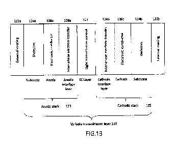
desired absorption
spectrum chemical modifications of chemical structures of cores of light-
absorbing compounds may be
carried out. A wide variety of functional groups may be introduced to organic
compounds to change
their properties, e.g. the absorption of visible light. Upon oxidation or
reduction of a precursor
compound having absorption in ion-radical form, one of the former frontier
orbitals (unoccupied LUMO
or fully occupied HOMO) turns into a single occupied SOMO, allowing
transitions from/to closely
located SOMO-N or SOMO+N orbitals. This phenomenon is responsible for the
bandgap of ion-radical
species being narrow causing strong absorption in visible range. In context of
chemical tuning of light-
absorbing compounds the influence of functional groups on the absorption of
ion-radicals should not be
accompanied by any significant effect on the precursor HOMO-LUMO bandgap width
and hence on the
absorption of non-radical colorless forms of corresponding electrochromic
materials. The introduction
of strong chromophore groups (e.g. -NR2, -OR, -NO2, -N=N-, etc.) is then not
favorable because they
may displace energy levels within the bandgap of a precursor and impart a
color to it. Moreover, these
groups may strongly affect the chemical properties and worsen the stability of
a precursor/ion-radical.
Varying the electronic substructure of precursors is better accomplished in
this sequence:
[0136] (1) Introduction of functional groups conjugated with the aromatic core
of a precursor, which
have a considerable number of ir-orbitals separated by a large bandgap (> 3.0
eV): phenyl, naphtyls,
biphenyls. This modification causes a strong shift of the color of an ion-
radical due to the insertion of
several energy levels below and above the bandgap of the precursor and
lowering the minimal distance
between the levels between which light-induced transitions are allowed.
[0137] (2) Modification of the aromatic substituent with inductive (-
CH3/alkyl/branched alkyl, -
CF3/fluorinated or perfluorinated alkyl/branched fluorinated or perfluorinated
alkyl, -F, -SF5, etc.) or
weak mesomeric (-0CF3, meta-OR', meta-NR'2, etc., where R' is an alkyl or
substituted alkyl, etc.)
donors/acceptors. These functional groups shift the positions of energy levels
or displace their levels so
that the bandgap of the precursor doesn't get significantly narrower.
Introducing the groups with very
CA 03158345 2022-04-14
WO 2021/075999 PCT/RU2019/000749
19
weak effects is used for the finest tuning of the absorption spectrum. Several
groups may be introduced
to attain the desired effect.
[0138] The special case of the modifications is those which provoke or
suppress the dimerization of
compounds prone to it: e.g., adding an aliphatic linker between two ion-
radical light-absorbing cores for
provoking the dimerization or introducing bulky substituents (a tert-butyl
substituent, for instance) for
suppressing the dimerization. The dimerization significantly changes the
absorption characteristics and
distorts the concentration dependency. It may also cause solvatochromic
effects.
Other purposes of chemical modification: The color tuning is not the only
purpose of the chemical
modification of precursors. The parameters able to be adjusted include: (1)
The mass-transport
properties, by adding bulky substituents; (2) The oxygen/water stability of
ion-radical forms (specific
for each case); (3) The redox potentials, by introducing substituents with
pronounced electronic effects
which shift the whole energy structure but don't make the bandgap
significantly narrower; (4) The
solubility, especially at low temperatures (specific for the matrix used); (5)
The rates of chemical
interactions between colored products of anodic and cathodic reactions (for
Types I/II).
[0139] In general, every substituent makes a complex effect on all the
properties at once, but some of
the consequences are more intense than others. Thus, a suitable modification
strongly depends on the
final purpose of the device.
[0140] Phenomenon of charge transfer, interfacial equilibrium: A fundamental
phenomenon of
electrochemical processes is interphase charge transfer. If two phases are
brought into contact, they form
an interface, at which electrochemical potentials of electrons, also denoted
as Fermi level (EF), in both
phases tend to equalize. The mechanism of EF equalization depends on types of
materials which form
an interface, though that process is always accompanied by electron transfer,
which must be
isoenergetic. (H. Gerischer in "Physical Chemistry: An Advance Treatise", Vol.
9A, H. Eyring. D.
Henderson, and W. Jost, Ed., Academic Press, New York. N.Y., 1970; (b) H.
Gerischer, Adv.
Electrochem. Electrochem. Eng., I, 139 (1961). Hence, for an electron transfer
to proceed there should
be a couple of occupied and vacant levels (states) of equal energy (within the
range of thermal
fluctuations, kT) in two phases that form an interface. In certain all-in-one
EC devices, initial
electrochemical reactions occur at the interfaces between an ionically
conducting (mostly, solution) EC
layer and electrodes, e.g., metal or semiconductor/dielectric layers of
electrodic stacks.
[0141] Solution side of an interface: A solution-type EC layer typically
comprises a liquid phase.
Electric conductivity in liquids except metal melts is provided by the mass
transport of ions, so the liquid
phase generally contains dissolved ionic compounds (i.e. electrolytes). An EC
layer can have interfaces
with conductive materials, their conduction being associated with the drift of
free electrons. Thus, at the
phase boundaries between electrodes and EC layer contacts of ionic and
electronic conductors arise. In
CA 03158345 2022-04-14
WO 2021/075999 PCT/RU2019/000749
the bulk liquid ionic conductor, under equilibrium conditions, the time-
average forces are the same in
all directions and at all points in the bulk electrolyte and there are no net
preferentially directed electrical
fields. However, the liquid phase is interrupted at the phase boundaries, so
the ion-ion and ion-solvent
interactions, which are uniform in a bulk liquid, become perturbed and the
electroneutrality is broken
down at the frontier. The excessive charge in a liquid phase produces the
electric field that interacts with
charged particles, of which an electrode is made. This interaction induces a
charge on the electrode.
Thus, a potential difference arises across the electrode interface, which is
then electrified. The
aforementioned interaction is known to form a specific interfacial structure
known as "double layer" or
"electric double layer" (hereinafter, EDL). Due to very low thickness of an
interface even low potential
differences may produce very strong electrical fields (on the order of 107
V.cm-1), which affect the
charged species in the interfacial region of the liquid. If an electroactive
solute is located at the interface,
a charge transfer to/from a solution energy state may occur, thus leading to
an electrochemical reaction.
[0142] Electron transfer to/from a solution: Solutes of small molecule
species, have discrete energy
spectra. Reversible redox processes of small molecule solutes involve electron
transfer from/to energy
levels of frontier orbitals of a solute (HOMO, SOMO or LUMO). However, for
electroactive solutes,
the energies of the solution states depend on whether the state is occupied
(Red) or vacant (Ox), owing
to the difference of solvent-sheath energies, X, around the Red and Ox
species. Since solvent molecule
exchange between the coordination sphere of the redox-active species and the
bulk electrolyte is a
dynamic process leading to a range of solvent sheath energies, the density of
redox states is best
described in terms of separate Gaussian distributions. The effective distance
of the electrode-electrolyte
electron transfer is supposed to have a value of OHP distance (which is
considered as the slippery plane),
because it's the closest position that an electroactive specie can reach in
the absence of the specific
adsorption (in this context only redox electrodes are discussed). Thus, the
driving potential difference
over the interface is the difference between the electrode surface (more
complicated for semiconductors)
potential and the potential of the OHP. The latter is determined by the
electrode type, its potential and
the properties of the electrolyte. The electrode may be connected to an
external electric circuit, so its
Fermi level may be changed; the electrolyte, as the medium that contain mobile
charge carriers, is known
to be polarized by an applied electric field due to the migration effect.
Thus, the electric field is
considered to penetrate the medium only to a certain depth, in the bulk medium
the electric field strength
being zero (figure). The thickness of non-electroneutral layer (and,
therefore, of EDL) depends on the
ionic strength of the solution and could be roughly estimated as a value of a
few Debye lengths. The
narrower EDL is, the higher driving potential difference arises between the
electrode and the OHP, thus
making the electron transfer more probable.
CA 03158345 2022-04-14
WO 2021/075999
PCT/RU2019/000749
21
[0143] Metal-electrolyte interfacial charge transfer: The conduction (CB) and
valence (VB) bands of a
metal are overlapped, so there are no forbidden energy levels for an electron.
The energy spectrum is
continuous and therefore Fermi level reflects the top order of energy that an
electron may have (taking
into account the thermal distribution around it). If any charge is introduced
to or withdrawn from a metal
its Fermi level changes due to the variation of the number of electrons in it
(ions are considered to be
immobilized in comparison with electrons), electrons occupying the levels of
lowest possible energies
according to the Fermi-Dirac statistics. If a metal is brought in a contact
with an electrolyte, which
contains electrochemically active solutes, their energy levels appear at the
electrolyte side. Some levels
are occupied once or twice, some are free. A pair of compounds that represent
reduced (donor, Red) and
oxidized (acceptor, Ox) forms of a specie form the redox couple. At non-zero
densities of Red and/or
Ox states at the interface a charge transfer is caused until the Fermi level
of the metal and redox Fermi
level of the electrolyte are equal. Every electron transfer must be
isoenergetic, thus, reduction of solutes
may take place if the Fermi level overlaps the regions of non-zero density of
Ox states and oxidation
may happen if the Fermi level overlaps the regions of non-zero density of Red
states. (H. Gerischer in
"Physical Chemistry: An Advance Treatise", Vol. 9A, H. Eyring. D. Henderson,
and W. Jost, Ed.,
Academic Press, New York. N.Y., 1970; H. Gerischer, Adv. Electrochem.
Electrochem. Eng., I, 139
(1961)).
[0144] Semiconductor-electrolyte interface interfacial charge transfer: In
contrast to metals, the CB and
VB of semiconductors (SCs) are not overlapped, therefore a range of forbidden
states is present (the
bandgap). An isoenergetic charge transfer may only happen if the energy levels
of non-zero densities of
acceptor (Ox) or donor (Red) states in the electrolyte match with the energy
levels of complementary
states in the semiconductor (electrons or holes). Thus, only those solutes
with energies near the
conduction or valence bands can exchange electrons with a semiconductor
electrode (in the absence of
such complicating factors as surface states or energy levels between the
conduction and valence bands)
(Journal of the American Chemical Society / 97.26 / December 24, 1975). Since
concentrations of charge
carriers in semiconductors may be 106-108 times lower than in a metal, the
densities of available states
in a semiconductor influences its electrochemical behavior: an intrinsic
semiconductor (at dark
conditions) may possess low concentrations of both electrons at CB and holes
at VB, so the rates of
charge transfer may be negligible; an n-type semiconductor has relatively high
amount of electrons at
the CB, so it can keep considerable rates of charge transfer to acceptor (Ox)
states; a p-type SC,
similarly, may efficiently withdraw electrons from donor (Red) states due to
relatively high
concentrations of holes at VB. However, degenerately doped semiconductors may
demonstrate metal-
like behavior if the potential exceeds the flat-band potential (Vfb) (more
negative for n-type, more
positive for p-type), so they may be used well both for reduction and
oxidation, but only for the solutes,
CA 03158345 2022-04-14
WO 2021/075999 PCT/RU2019/000749
22
which Ox and Red states energies are higher than Vfb (for n-type SC) or lower
(for p-type SC) (Journal
of the American Chemical Society / 97.26 / December 24, 1975).
[0145] Transparent Conductive Oxide (TCO) electrodes: Transparent Conductive
Oxide (TCOs), being
degenerately doped semiconductors having quasi-metallic conductivity, possess
the wide bandgap
(-3.0 eV or more), making them barely interactive with visible light. Most
widespread TCOs are n-type,
so to keep the ability to oxidize and reduce the solutes at the interface, the
range of potentials that provide
metal-like electrode behavior are preferred. To obtain better performance and
to widen the variety of
usable solutes, high work function materials are preferable for anode. Quasi-
metallic conductivity gives
low ohmic resistivity and specific interfacial properties, so TCOs may combine
functions of surface
conduction and interfacial charge transfer; however, additional surface
conductive layers and/or
interfacial layers may still be introduced to the electrodic stacks that
contain TCOs.
[0146] Semiconductor interface effects: The peculiarities of semiconductors
(SC) may be used to
control the electrochemical processes on the electrodes of a variable
transparency layer. For example,
using a sufficiently low work function SC at the cathodic interface (e.g., a
bare SC conductive layer or
with one or more interfacial layers) may block oxidative processes except
those of reduced states of
initially electroreduction-sensitive compounds. This allows use of fast
discharging of the variable
transparency layer by applying strong reverse overpotentials as in, for
example, a TYPE II device
(described more fully below).
[0147] In addition, reverse electrochemical processes of electrochemically
generated species on the
counter electrodes may be suppressed by using a SC interface (see Type II
device below).
[0148] Mass transfer, ion transfer: Every interfacial charge transfer converts
a reduced specie to an
oxidized one in case of electrooxidation and vice versa in case of
electroreduction. Once the electrolyte
redox Fermi level is shifted via a charge transfer, the concentrations of
reagent/product solutes at the
interface changes (in comparison to bulk electrolyte), thus causing the
concentration gradients and hence
the diffusional fluxes. Moreover, electron transfer at the interface leads to
the emergence of the
uncompensated excessive charge within the electrolyte at the OHP, which
contributes to the electric
field. Every charged specie interacts with it, causing electromigration. The
uncompensated charge in the
electrolyte changes the driving voltage over the interface (Frumkin effect,
see above). The solution
components interact with the electrostatic field induced by the charge,
causing the reorganization of the
surrounding medium, forcing ions to migrate and solvent dipoles to reorient.
The rate of the charge
compensation depends on dielectric constant of the solution and on the rates
of the ion transfer.
[0149] If the charge transfer rate exceeds the rate of mass transfer of a
reagent solute, the overall rate of
electrochemical reaction (and hence the total electric current) becomes mass-
transfer dependent. Thus,
the mass transfer of the reagent solutes contributes significantly to the
reaction rates. In most cases, the
CA 03158345 2022-04-14
WO 2021/075999 PCT/RU2019/000749
23
rates of the charge transfer steps are higher than the rates of the mass
transfer. The proper mass transfer
rates affect optimization of the performance of an EC device: too high rates
of mass transfer may lead
to excessive electric currents and power consumption (which may lead to the
high ohmic drop on the
electrodes and hence to the EC device malfunction), whereas too low mass
transfer rates may cause
extremely long switching times and poor optical characteristics. The rates of
mass transfer processes are
able to be set by varying the matrix and chemical tuning of solutes structures
for a given application.
[0150] Concerning ionic compounds, significant contribution to mass-transfer
rates are given by the
phenomenon of ionic association. Strong ionic association reduces solubility
and may drastically worsen
the mass-transfer rates. Hence, an EC composition or layer are preferred to
include at least one weakly
coordinating ion (cation/anion or both, see below).
[0151] Convection: If the electrolyte is liquid, the mass transport mechanisms
are not limited to the
diffusion and migration. Thermal effects of chemical and electrochemical
reactions, the operational
temperature difference between the parts of an EC device (which may arise due
to the various heat
release along an optical path by light absorbing compounds, and over the
exposed surface), the
dependence of the density on the concentrations of the species dissolved, and
other factors may cause
the bulk flows within an EC layer, thereby causing convection effects (e.g.
Rayleigh-Benard cells, color
splitting, etc). In an EC device this may cause the transmittance fluctuations
and gradients, high
operational currents and therefore is desirable to be suppressed by adjusting
the rheology of the EC
layer.
[0152] Charge Conservation: If an electrochemical reaction happens on an
electrode-electrolyte
interface, the excessive charge that is formed on the electrode must be
withdrawn by an external electric
circuit (e.g., the control circuitry). To allow the current flow through an EC
device the charge receiving
portion must be electrically coupled with the first electrode. Because the
initial process is a Faradaic
charge transfer from an ionic conductor to an electronic one, to preserve the
electroneutrality of an EC
layer the system must contain a second contact of electronic and ionic
conductors that allows the
complementary Faradaic charge transfer from the electrode to the EC layer.
Therefore, typical all-in-
one EC devices can be represented by an electrochemical cell that contains at
least two electrodes (anode
and cathode) and an EC layer that contains at least one compound that is
sensitive to the electrooxidation
and one sensitive to electroreduction. However, there is no need for an anode
and cathode to be both
transparent or to be located within an optical path for light transmittance.
In certain aspects of EC devices
of the present disclosure, only one electrode is located within an optical
path for light transmittance and
in contact with an EC composition or layer in order to produce/consume colored
species over the
composition or layer. In such a case, the second substrate defining the
optical path may not have any
electrode or electrodic stack or may have the anodic or cathodic electrode as
the first substrate (e.g., two
CA 03158345 2022-04-14
WO 2021/075999
PCT/RU2019/000749
24
optically transparent anodes or two optically transparent cathodes). The
second electrode may be located
within any auxiliary volume ionically conjugated with the EC composition or
layer, for example.
[0153] As explained above, the present disclosure is directed to, among other
aspects, electrochromic
devices and components thereof and systems and methods for controlling
electrochromic devices.
Referring now to the drawings, Fig. 1A depicts an exemplary electrochromic
device 100. As shown in
the figure, controller 110 is electrically connected to variable transmittance
layer 120 via electrical
connections 112a, 112b and bus bars 130a and 130b, respectively. Controller
110 can include circuitry,
and optionally software, to apply an input signal to the variable
transmittance layer. The variable
transmittance layer 120 can include an EC layer disposed between two optically
transparent substrates,
at least one of which includes an electrically conductive surface forming an
electrode. For this particular
example, variable transmittance layer 120 includes two optically transparent
substrates each of which
includes an electrically conductive surface forming electrodes. In this
example, bus bars 130a and 130b
are on and electrically in contact with each of such electrodes.
[0154] There may be more than one connection on each electrode, and different
connections can have
different functions. For example, some of the connections may have the Signal
function while others
may have Sense function.
[0155] Electrochromic activity of device 100 is provided by the variable
transmittance layer 120. The
variable transmittance layer may include one electrodic stack, a bare
dielectric substrate and an EC layer,
or two electrodic stacks and the EC Layer therebetween. An exemplary variable
transmittance layer 120
structure is depicted in Fig. 1B. For example, as depicted in FIG. 1B, the
variable transmittance layer
120 may include dielectric substrates 124a and 124b, anode 126a, cathode 126b,
and an electrochromic
layer 121 for controlling light transmission. An anodic interface layer (or
anode-side inter-phase electron
transfer layer) 128a, and/or a cathodic interface layer (or cathode-side inter-
phase electron transfer layer)
128b, can optionally be included in the variable transmittance layer. Further
external coatings 122a and
122b, can optionally be on dielectric substrates 124a and 124b, respectively.
[0156] The EC layer 121 provides the ability of transmittance alteration when
an electric bias is applied
between it and the electrodic stacks 123 and 125 that are in contact with it.
The control system can
include circuitry to apply an input signal though the electrical connections
and electrodes in contact with
the electrochromic layer. The input signal can include, for example, a certain
voltage, e.g., less than
about 1.5V, preferably below about 1.3V and more preferably below about 1.2V,
such that light
transmission of the electrochromic layer changes from one state (e.g., a high
light transmission state) to
another state (e.g., a low light transmission state).
[0157] The functions of these elements are as follows:
CA 03158345 2022-04-14
WO 2021/075999
PCT/RU2019/000749
[0158] The outer surfaces of the substrates of the variable transmittance
layer 120 may be optionally
covered with one or more functional coatings (e.g., external coatings 122a,
122b) such as, for example,
anti-glare, index matching, antireflective coatings, low emissivity (low-e)
coatings; radiation filters
(UV/NIR blockers, color filters); scratch-resistant or armoring coatings;
hydro-, oleo- or omniphobic
coatings; adhesives (may hold the index matching functions for a specific
material on which the EC
device is supposed to be applied); etc.
[0159] Dielectric substrates 124a/124b of the electrodic stack of the variable
transmittance layer are
high optical transparency, low haze structural element. The substrates may be
made of glass, plastic
(bulk or film) or transparent ceramic in various embodiments. In some
embodiments bus bars (described
elsewhere herein) are added to the substrate and are electrically connected to
the respective electrodes
(anode 126a or cathode 126b). In an embodiment, the substrate may include one
solid layer, for example
a sheet of glass. Alternatively, the substrate may include multiple layers
such as, for example, a
laminated glass triplex. Such construction could be beneficial for safety. The
substrate may also provide
other functions.
[0160] Glass is a preferred transparent dielectric substrate for many
applications. It typically has
superior transparency, low haze and structural stability. If it is not
compromised structurally, it is
impervious to gasses and liquids, making it an excellent barrier to protect
sensitive compounds.
[0161] There may often be rigorous requirements for operational stability and
safety for glass. These
functions are typically accomplished by using tempered glass, heat treated
glass and/or glass laminated
with safety interlayers. Such glass substrates can be used in the EC devices
of the present disclosure.
[0162] Tempering is heat treatment of glass sheets including in heating them
to a temperature above the
560 C, followed by rapid cooling using air flow. Tempering is performed in an
oven where glass is
transported to by rollers. The imprint of the roller structure typically
results in a wavy shape of tempered
glass, potentially leading to optical distortions. One way to reduce such
unwanted distortions is to
laminate two tempered glass sheets together with peaks of one glass sheet
matched generally against the
valleys of the other sheet. Hence in an aspect of the present disclosure, EC
devices can include as one
or more optical substrates a first tempered glass sheet laminated to a second
tempered glass sheet with
peaks of the first tempered glass sheet matched generally against valleys of
the second tempered glass
sheet.
[0163] Tempered glass has higher mechanical strength than regular, annealed,
glass. Once tempered
glass breaks, it disintegrates into multiple small pieces of glass containing
few sharp edges, thereby
accomplishing safety function. Majority of automotive side and rear windows
are made from tempered
glass.
CA 03158345 2022-04-14
WO 2021/075999
PCT/RU2019/000749
26
[0164] Lamination of glass is another method to accomplish safety function.
Two sheets of glass are
joined together using an interlayer sheet. The assembly is then treated with
temperature and/or pressure,
often accompanied by vacuum degassing to remove any air bubbles. Two most
common classes of
interlayer sheets are made from Polyvinyl Butyral (PVB), and Ethylene-Vinyl
Acetate (EVA).
Laminated glass, once broken, remains attached to the interlayer, thereby
accomplishing safety function.
[0165] In some embodiments, transparent plastics are used as substrates for
electrochromic devices.
Their advantages relative to glass are, for example, low weight, flexibility,
if made in form of a film,
high volume processing, for example in the roll-to-roll format, etc. On the
other hand, plastics also have
some disadvantages such as a generally lower optical quality compared to that
of glass, lower optical
and electrical quality of transparent electrodes, gas and water vapor
permeability, probable long-term
chemical reactivity with components of an electrochromic composition or, UV
susceptibility resulting
in degradation, lower temperature stability which can limit processing
options, etc.
[0166] Plastic substrates suitable for electrochromic devices and applications
of the present disclosure
can be formed from, but are not limited to, Polyethylene Terephthalate (PET),
Polytetrafluoroethylene
(PTFE), Perfluoroalkoxyalkane (PFA), Polyethylene naphthalate (PEN),
Polycarbonate (PC) and others.
In order to reduce or eliminate chemical reactivity of plastics with EC
materials surfaces in contact with
EC materials may be passivated with an inert material.
[0167] In some embodiments, the substrates are transparent ceramics.
Transparent conductive
electrodes are deposited on the surface of such substrates by the same methods
as onto glass.
[0168] An optically transparent electrodic stack (e.g., anodic stack 123
and/or cathodic stack 125) in
conjunction with an EC layer 121 keeps electrochemical processes at the
electrode-electrolyte interface
over the area of the variable transmittance layer 120. In the example of Fig.
1A, the electrodic stack
includes at least one surface conductive layer, e.g., anode 126a and/or
cathode 126b, to keep the surface
currents with sufficiently low ohmic drops.
[0169] The anodic and cathodic surface conducting layers may be formed of
transparent conducting
electrodes such as OTEs. OTEs are widely used in the industry today, enabling
a variety of devices used
across a myriad of applications such as photovoltaics, flat screens, touch
screens, heated transparent
surfaces, EMI shielding and others. OTEs are typically characterized by their
optical and electrical
properties.
[0170] Optically, desired properties of OTEs relate to transparency (higher
values are desired), color
(neutral is preferred) and haze (lower values are desired).
[0171] Electrically, the property of interest of an OTE is sheet resistance,
measured in the units of
Ohm/square. Some applications, for example capacitive sensors for
touchscreens, need relatively high
sheet resistance, on the order of hundreds of Ohms/square. Electrochromic
devices are typically low
CA 03158345 2022-04-14
WO 2021/075999 PCT/RU2019/000749
27
voltage devices that consume considerable currents, and therefore resistive
losses need to be minimized,
driving the requirements for low sheet resistance preferably below about 100
Ohms/square, e.g., below
about 70 Ohms/square, such as less than about 50, 30, 20, 15, 10, 5
Ohms/square.
[0172] The main classes of OTE include OTEs made from transparent oxides,
commonly called
Transparent Conductive Oxides (TCO). Examples of TCOs include, but are not
limited to, indium tin
oxide (ITO), aluminum doped zinc oxide (AZO), fluorine doped tin oxide (FTO),
molybdenum oxide
(Mo03), indium zinc oxide (IZO), indium gallium zinc oxide (IGZO), tin zinc
oxide (TZO), tin oxide
(Sn02), aluminum doped tin oxide (ATO), zinc oxide (Zn0), indium oxide
(In203), gallium oxide
(Ga203), zinc doped tin oxide (ZTO), indium doped gallium oxide (IGO), gallium-
indium doped tin
oxide (GITO), gallium doped zinc oxide (GZO), zinc doped indium tin oxide
(ZITO), zinc indium oxide
(ZIO), gallium doped indium oxide (GI), copper aluminate (CuA102), etc. Most
common ones are
Indium-doped Tin Oxide, ITO, and Fluorine-doped Tin Oxide, FTO.
[0173] Other suitable of OTEs include, for example, thin layers of metals and
metal meshes or grids
(e.g., meshes or grids of metal nanowires). Thin layers (thinner than the
characteristic wavelengths of
visible light) of metals (e.g. silver or gold) are transparent and have great
electrical conductivity.
Sometimes these metals are alloyed with other metals reduce cost and improve
chemical stability. Metals
may be deposited as thin films or as nanoparticles from vapor or liquid phase.
Properly designed metal
layers may possess reflective properties in IR range, so an OTE having such
layer can be used as a low-
emissivity coating in addition to its primary functionality of electrical
conductivity.
[0174] In some embodiments, hybrid OTEs, made by combining the layers of TCO
and metals are used.
The advantages of such hybrid construction include reduced overall stack
thickness and improved
optical properties for a given resistance or lower resistance for a given OTE
thickness.
[0175] Other suitable materials for OTEs include, for example, carbon
materials (e.g., single-walled or
multi-walled carbon nanotubes, graphene); conductive polymers; conductive
metal-organic or covalent
organic frameworks (M0Fs/C0Fs); or conductive metallocomplexes. It will be
appreciated that the
aforementioned materials may be mixed or stacked in a cathodic or anodic
surface conducting layer and
that the anodic and cathodic stacks may differ from each other.
[0176] Because EC devices have a source of electricity connected to them, one
possible functionality to
incorporate in such devices is a defogging capability. Defogging of an EC
device can be achieved by a
configuration including a heating element thermally connected to the device.
Defogging can occur either
by heating a substrate or external coating thereof of the device, or by
heating an OTE of the device itself.
If an OTE of the device is heated, it is important to minimize or avoid
adverse effects towards
electrochromic layer. The adverse effects may stem from elevated temperature,
and from
electrochemical processes. One way to avoid undesired electrochemical
processes is to accomplish
CA 03158345 2022-04-14
WO 2021/075999
PCT/RU2019/000749
28
heating with alternating current, AC (as opposed to DC driven operation of the
electrochromic device)
at frequencies exceeding the frequencies corresponding to characteristic
diffusion time constants of the
electrochromic reaction in the device.
[0177] It will be appreciated that in view of the EC applications, OTEs
desirably preserve their structural
integrity and not react with chemicals from the EC layer 121 within the
operation ranges of
overpotentials. The issue of structural integrity is especially pronounced for
OTEs on flexible substrates.
For example, if ITO is deposited on PET, it may crack upon handling/bending.
Generally, ITO is stable
relative to EC chemistry. However, crack formation may change local
stoichiometry of ITO and its
dopants, resulting in increased reactivity with EC chemistry, which leads to
rapid device degradation.
Even without chemical degradation the formation of cracks may render the
device inoperable as the
distribution of electric potential is no more homogenous across the surface of
the device. Such
inhomogeneity results in patchy coloration of the device and to other optical
defects.
[0178] From the chemical compatibility point of view, some OTEs based on metal
may not withstand
contact with EC components within the operation ranges of overpotentials. For
example, silver and
copper are corroded away rapidly under such conditions. Other metals and metal
alloys are more stable,
including gold, palladium, platinum, iridium, Hastelloy and some other metals
and alloys. One way to
protect metal OTEs in EC applications is to use them in hybrid, multilayer
arrangement together with
TC0s, e.g., an OTE/metal OTE/OTE layered structure on an optically transparent
substrate. For
example, such hybrid electrode could include a layer of ITO on a flexible
substrate, followed by a thin
layer of silver, followed by another layer of ITO, e.g., an ITO/silver OTE/ITO
layered structure on an
optically transparent substrate. The outer layer of ITO acts as both a part of
an OTE and as a protective
layer for silver, preventing direct contact between silver and an EC layer.
[0179] Another option is to use specialty anodic and/or cathodic interface
layers. Such layers may not
form a good OTE by themselves, but they would provide protection for the metal
layer of OTE without
substantially impeding the electric circuit. One option for such layer is to
make it from a suspension of
carbon nanotubes. However, the purpose of an interface layer is not limited to
protecting an OTE (see
below).
[0180] Where an EC device has two stacks (residing on two substrates), there
is no requirement that the
stacks and substrates should be identical. Indeed, in certain applications and
device structures it may be
advantageous to have one stack differ from another. The following are examples
of such asymmetric
arrangements and the benefits thereof.
[0181] Several applications of EC devices are asymmetric in terms of the
environment in which they
operate. In case of architectural windows, for example, the inside and outside
of the window have very
different environments. The sun load is acting from the outside, therefore
majority of UV and IR load
CA 03158345 2022-04-14
WO 2021/075999 PCT/RU2019/000749
29
are impinging the surface of the EC device that is facing the outside.
Therefore, it may be preferred to
have the externally facing substrate differ from the internally facing one.
For example, the externally
facing substrate may have additional features such as UV absorption and/or IR
reflectivity. Such features
may be implemented either as a separate layer of the stack belonging to the
externally facing substrate,
or may be incorporated into the bulk of the substrate (for example, as UV
absorbing additives within a
plastic substrate). Another light control feature that can be optionally added
to the externally facing
stack is polarization control. By having the substrate, or one of its layers,
act as a polarizer, the overall
sun load and glare can be reduced. Hence in an aspect of the present
disclosure, an optically transparent
substrate, preferably an externally facing substrate, polarizes light or
includes a layer thereon that
polarizes light.
[0182] Another type of possible asymmetry is in two substrates made from
different materials. For
example, in case of AR goggles, one of the substrates may be a relatively
thick polycarbonate lens, while
the other one is a lightweight film, e.g. PET.
[0183] In case of windows, one substrate may be glass, while the one may be
film-based. Such an
arrangement is possible for example in an insulated glass unit (IGU) assembly,
where a film-based
substrate would face an inner cavity of an IGU containing an inert atmosphere.
In this case, since the
film-based substrate is facing an inert environment the edge and area sealing
requirements may be
relaxed if not completely removed. This simplifies device complexity and
reduces cost. FIG. 1C and its
description below provides additional details of such an IGU.
[0184] The surface conductive layer 126a/126b provides an interphase charge
transfer to an interfacial
layer 128a/1 28b (respectively) or to a solution where the variable
transmittance layer does not include
interfacial layers. The anodic and cathodic interface layers 128a/1 28b adjust
the charge transfer behavior
at the electrode-electrolyte interface (anodic and/or cathodic) and hence may
not have high surface
electronic conductivity. The interfacial layers can be formed of, for example,
monomeric/polymeric
organic semiconductors; inorganic semiconductors; organic dielectrics;
inorganic dielectrics; MOFs;
carbon materials (e.g., single-walled or multi-walled carbon nanotubes,
graphene); physically or
chemically adsorbed or bonded molecular layers of electrochemically active
compounds (which may
act like immobilized redox shuttles); or physically or chemically adsorbed or
bonded molecular layers
of electrochemically inert compounds that modify the solution properties at
the interface (e.g. dielectric
permeability, ionic strength, ionic association, etc.).
[0185] Interface layers may also be used to modify mechanical, optical or
other non-electrical properties
of the interface, e.g. interfacial adhesion, index matching or electrode
surface wettability. During
fabrication of the variable transmittance layer, one or more interfacial
layers 128a/128b of electrodic
CA 03158345 2022-04-14
WO 2021/075999 PCT/RU2019/000749
stacks 123/125 may be used pre-assembled or may be partially or fully self-
assembled in situ during the
fabrication.
[0186] Regardless of the type of the EC device, the EC layer 121 can include
one or more of light
absorbing compounds. The EC layer 121 can further include one or more of
auxiliary compounds,
modifiers, matrix, solvent, supporting electrolyte, polymer additive(s), and
additional components.
[0187] As explained above, an electrochromic device can be asymmetrical in
that the opposing
substrates are made from different materials. For example, one optically
transparent substrate can be a
glass while an opposing optically transparent substrate can comprise a
flexible materials such as a
polymer, e.g., a PET film. Alternatively, the EC device can include optically
transparent substrates made
from two different types of glass, two different thickness, two different
chemical compositions and/or
differing type of OTEs on the substrates if both have an OTE. In addition to
certain electrooptic
performance advantages, such a device structure has advantages for integration
into window assemblies
such as insulated glass units (IGUs).
[0188] In general, an insulated glass unit includes a first glass substrate
and a second glass substrate
which define a chamber having a volume therebetween. The chamber can include
an inert atmosphere
and the chamber can also include part of, or all of, one or more
electrochromic devices. Such a
configuration can allow one or more edges of the electrochromic device to be
exposed to an inert
atmosphere and/or where at least one of the first glass substrate or the
second glass substrate of the IGU
is not in electrical communication with the electrochromic device.
[0189] FIG. 1C illustrates a cross-section of an IGU according to an aspect of
the present disclosure. As
shown in the figure, two opposing substrates (e.g., first glass substrate 1010
and second glass substrate
1012) are spaced apart and sealed at edges thereof with sealing elements 1014a
and 1014b to form an
interior chamber (1016) having a volume. The opposing substrates (1010 and
1012) are optically
transparent and can be made of the same material or different materials or
different thicknesses
including, a glass, plastic or any of the other substrates suitable for an EC
device. The sealing elements
can be formed using methods and materials common in the window industry.
Advantageously, interior
chamber 1016 can contain an inert atmosphere. An inert atmosphere as used
herein is an atmosphere
including substantially an inert gas, e.g., nitrogen, argon, etc. or
combinations thereof. While FIG. 1C
illustrates an IGU with two substrates, e.g., two glass panes, additional
substrates can be included in the
structure such as three or more glass panes. For example, there can be an
assembly with three or more
glass panes, each spaced apart, e.g., the third substrate can be spaced apart
from the second and defining
a second volume with an inert atmosphere.
[0190] In an aspect of the present disclosure, one or more EC devices can be
formed, in part or in whole,
within the interior of an IGU such that the EC device is exposed to, and thus
protected by, an inert
CA 03158345 2022-04-14
WO 2021/075999 PCT/RU2019/000749
31
atmosphere of an IGU having an inert atmosphere. As illustrated in the example
of FIG. 1C, the IGU
further includes an EC device. In this embodiment, the EC device is formed
with a substrate that forms
the IGU. In particular EC device 1200 includes a first optically transparent
substrate (1210) with a first
optically transparent electrode (1212) disposed thereon a second substrate
(1012) with a second optically
transparent electrode disposed thereon (1216) and an electrochromic
composition (1218), e.g., an EC
layer, disposed between the first and the second substrates.
[0191] Advantageously, since the EC device 1200 is formed in part within the
interior chamber of the
IGU, at least the first optically transparent substrate (1210) of the device
has edges (1214a and 1214b)
exposed to the inert atmosphere. Since the interior atmosphere of the IGU is
chemically inert it is
therefore not necessary to form a seal around the edge of the EC composition
so long as the EC
composition is not mobile. Alternatively, the edge of the EC composition can
be sealed, but the oxygen
and moisture barrier requirements for such a seal would be drastically lower
as compared to those of an
assembly that is exposed to an oxygen atmosphere. In addition, since the
second optically transparent
substrate (1218) of the device is not part of the structure of the IGU, it can
have properties that are not
required for a window and can comprise a form and composition of a flexible
film, etc.
[0192] In the example illustrated in FIG. 1C, the second optically transparent
substrate (1012) of the EC
device has a second edge that is not exposed to the inert atmosphere (1012a,
1012b) but instead sealed
with sealing element 1014a and 1041b respectively. While FIG. 1C illustrates
an EC device formed in
part with an exterior substrate of the IGU, the EC device can be formed with
components within the
interior chamber (1016), such as, for example, EC device 1200 which
substitutes the exterior substrate
of the IGU (1012) for a second optically transparent substrate having an OTE
thereon but within the
interior chamber (1016) with edges exposed to the inert atmosphere, e.g., an
additional substrate within
the chamber to form the EC device. In such a configuration, the exterior glass
panes of an IGU do not
form part of an EC device and thus pane does not participate in the EC
functionality, while other panes
may contain EC devices.
[0193] In addition, more than one EC device can be included in the interior
chamber of an IGU. Such
multiple devices can operate independently, meaning that their optical state
may be varied individually.
One reason to operate multiple EC devices independently is to achieve greater
dynamic range of tinting.
For example, if two EC devices individually have minimum VLT of 10%, then the
effective minimum
VLT with both devices having their minimum VLT state would be 1%. Another
reason to operate
multiple EC devices independently is to have them tuned to different colors,
and therefore change the
visual appearance of the window on demand.
CA 03158345 2022-04-14
WO 2021/075999
PCT/RU2019/000749
32
[0194] The EC devices formed with IGU further include components to operate
the EC device such as
a control system or controller electrically connected to the first and second
electrodes to apply an input
signal to the EC composition.
[0195] FIG. 2 illustrates several device configurations according to certain
implementations of the
present disclosure. The devices include a cathode, an anode, and an
electrochromic composition in
various configurations. For the devices illustrated in FIG. 2, the
electrochromic composition is disposed
between and in contact with the cathode and the anode and configured to change
light transmission from
one state to another state (e.g., change visible, infrared light transmission
and/or UV light transmission
from a high state to a low state transmission) in response to an input signal
between the cathode and the
anode.
[0196] For example and as shown in FIG. 2, a Type I device includes a first
substrate (210) having a
first electrode (212), e.g., an anode, a second substrate (220) having a
second electrode (222), e.g. a
cathode, and an electrochromic composition (230) disposed between the first
and the second substrates
and edge seals, which in this configuration are oppositely configured (240a,
240b). Such edge seals
protect the electrochromic composition and can prevent leaking thereof from
between the substrates.
The first and second electrodes can include interfacial layers. For this
example, the electrodes and
optional interfacial layers do not have electrochromic selectivity. The first
optically transparent
substrate (210) and the second optically transparent substrate (220) and the
electrochromic composition
therebetween (230) define an optical path for light transmittance (211).
[0197] As shown for this example, a Type I device is a planar thin-layer cell
with an isotropic EC layer
sandwiched between two oppositely biased, optically transparent electrodes
(anode, cathode). In such
an EC device, the diffusional fluxes of the species that are formed on the
opposite electrodes have non-
zero projections in the normal direction relative to the electrodes. Because
the anodic and cathodic
reactions occur on the electrodes that are separated only by an EC layer, the
ion transfer distances are
of order of the EC layer thickness. If species that were formed on the
positive biased electrode reach the
negative biased one (and vice versa) and their electrochemical behavior is
reversible within the
operational range of potentials, it is readily converted back to its precursor
due to very high reverse
overpotential maintained and the back flux of the precursor appears. Due to
the very high reverse
reaction rates on the counter electrodes, the concentrations of species that
were produced in the
complementary reaction chain are close to zero (reagent depletion) and highest
concentration gradients
(and hence the preferred direction of the diffusion mass-transfer) appear in
the direction to the so-called
consuming boundary, i.e. the counter electrode. As the cell is planar, this is
the normal direction
relatively to the electrode. It means that the lateral travel of an
electrochemically generated solute is in
most cases negligible in comparison to the linear size of a variable
transparency layer.
CA 03158345 2022-04-14
WO 2021/075999 PCT/RU2019/000749
33
[0198] So, an EC device of such a construction usually does not allow the full
electrochemical
conversion of reagents to products. In other words, a Type I EC device is
monostable and consumes
considerable current in every state except at open-circuit conditions. One
additional peculiarity is that
two species, which are the members of the anodic and cathodic reaction
sequences may react within the
EC layer with formation of their precursors (due to the reversibility of all
chemical or electrochemical
processes), causing chemical self-discharge. Thus, if such an EC device is
left open-chained after
biasing, it will likely self-discharge in a relatively short period of time.
However, the self-discharge
processes are only ones that cause normally directed difftisional mass-
transfer at open-circuit state
(relative to the inner electrode surface), so the lateral transfer may
contribute significantly at open-circuit
state if the rates of self-discharge processes are low. Another feature of a
Type I EC device is that if at
least two zones (near the same electrode) of different interfacial ratios of
reagents and products of
electrochemical reactions are present the potentials of the same electrode at
these zones will differ what
will cause the electric current through this electrode and will tend to align
the differences through the
electrochemical reactions.
[0199] For a monostable EC device the rates of consumption of light-absorbing
species are lower than
the rates of their formation. Otherwise, the quasi-stationary concentrations
of the light-absorbing species
are negligible over the whole EC layer and no transmittance change occurs
despite the current still being
consumed. Thus, for a Type I EC device, only the mode of operation that is
fully transparent at an off
state is viable due to the difficulty of obtaining full electrolysis of
electrochemically active reagents.
[0200] Therefore, for a Type I EC device some preferred characteristics for
light-absorbing compounds
may be present: if an EC device uses more than one light-absorbing compound
and at least one OTE
operates in the reagent mass-transfer limiting mode, the diffusion
coefficients of electrochemically
active precursors reacting on that electrode are to be matched to get the
identical distributions of light-
absorbing compounds concentrations at transients. If both electrodes operate
in reagent mass-transfer
limiting mode, all the precursors are to be matched in terms of diffusion
coefficients. Otherwise, due to
the different current distributions on anode and cathode (due to the
diffusional control of the electrodic
processes and Ohmic drops on surface conductors), color deviations may arise
at transients and/or at
intermediate levels of tint (as has been further explained elsewhere herein).
As discussed elsewhere
herein, chemical modifications of the cores of light-absorbing compounds and
their precursors are to be
used to modify the diffusion coefficients.
[0201] The effects of unequal diffusion rates of reagents described above can
be mitigated or avoided
by: (1) using a distributed (multi-point) connection of electrodes to the
control circuitry to minimize
Ohmic drops across the electrodes; and/or (2) setting both electrodes to
operate at ion-transfer limiting
conditions (via Frumkin effect). The latter is attained by proper adjustment
of an electrochromic
CA 03158345 2022-04-14
WO 2021/075999
PCT/RU2019/000749
34
composition, ionic conductivity of the composition and electrochromic species
concentrations. Both
approaches listed above can be used for mitigating the "iris" effect. Hence,
in an aspect of the present
disclosure, EC devices of the present disclosure can include a control system
or controller to apply an
input signal to an electrochromic composition or layer, wherein the controller
is electrically connected
to one or more electrodes of the device in contact with the electrochromic
composition or layer by
distributed, multi-point electrical connections to minimize ohmic drops across
the electrodes. In
addition, or in the alternative, the controller can be configured to operate
both electrodes at ion-transfer
limiting conditions of the electrochromic composition or layer. A
configuration that includes
distributed, multi-point electrical connections to one or more electrodes
and/or a controller configured
to operate both electrodes at ion-transfer limiting conditions can be included
in all EC devices of the
present disclosure.
[0202] FIG. 2 further illustrates a Type II EC device, which includes a first
substrate (210) having a first
electrode (252), e.g., an anode, a second substrate (220) having a second
electrode (262), e.g. a cathode,
and an electrochromic composition (230) disposed between the first and the
second substrates and in
contact with the first and second electrodes (252, 262). The Type II device
also includes edge seals,
which in this configuration are oppositely configured (240a, 240b). In this
example, one or both of the
electrodes can suppress unwanted electrochemical processes in the EC
composition, e.g. wherein either
or both of the cathode electrode or anode electrode selectively allows
substantially only a reduction or
an oxidation of the specific components of the electrochromic composition.
Such electrodes can have,
as a surface exposed to the electrochromic composition, a semiconductor
material. In such a
configuration, either or both of the cathode or anode comprises a
semiconductor material at an interface
with the electrochromic composition.
[0203] A Type II EC device is similar to a type I EC device except unwanted
processes on the electrodes
are suppressed, thereby allowing to execute the full electrolysis of species
in the electrochromic
composition. In a Type II EC device, chemical self-discharge processes remain,
so the device is still
monostable. However, if the rates of self-discharge processes are negligible,
it is possible to operate this
type of EC device in both straight and reversal modes (fully transparent or
fully darkened at off state).
Thus, the device may also be considered and controlled as a bistable device
(i.e. substantially zero power
consumption in any state, power is consumed only to switch between states).
[0204] In a Type II EC device no significant normally directed diffusional
fluxes are present if the self-
discharge rates are low. Accordingly, the lateral diffusional mass-transfer
distance can be considerable
in comparison to the transverse linear size of the variable transmittance
layer even at biased states, as
opposed to the Type I EC device.
CA 03158345 2022-04-14
WO 2021/075999 PCT/RU2019/000749
[0205] FIG. 2 further illustrates a Type III EC device, which includes a first
substrate having a first
electrode, e.g., an anode, a second substrate having a second electrode, e.g.
a cathode, and an
electrochromic composition disposed between the first and the second
substrates and edge seals, which
in this configuration are oppositely configured. The substrates, electrodes,
electrochromic composition
and edge seals can be configured as described in Type I and Type II devices
above.
[0206] A Type III device of the present disclosure, however, includes a
partially permeable additional
element within an EC layer. For example, a Type III device can include a
membrane within the EC
composition, e.g., EC layer, which is selectively permeable. As shown in FIG.
2, the electrochromic
device can include selectively permeable membrane (270) disposed between the
cathode electrode and
anode electrode.
[0207] In such a configuration, the membrane can substantially allow
permeation of small ions but
substantially prohibits permeation of large ions. For example, the membrane
can substantially allow
permeation of protons but substantially prohibits permeation of ions larger
than protons. Alternatively
or in combination, the membrane can substantially allow permeation only of
electrochemically inert
ionic species of supporting electrolytes, but to not the reactive species.
[0208] Under certain selectivity of membrane within the electrochromic
composition, an electro-
generated solute cannot reach the counter electrode or get in contact with
chemically reactive species
that form on it. Therefore, no significant self-discharge or reverse
electrochemical reaction rates are
present. A Type III EC device can allow full electrolysis and hence is
bistable. As with a Type II EC
device, the tangential diffusional mass-transfer distance is considerable in
comparison to the linear size
of the variable transmittance layer.
[0209] In an aspect of the present disclosure, a selectively permeable
membrane can have a center
portion and a peripheral portion in which the center portion has a higher
permeability than the peripheral
portion. Such a membrane can be fabricated by having a thicker peripheral
portion or a peripheral
portion made from a lower permeable material. In this way, such a membrane
included in an EC layer
and between electrodes of an EC device would result in an anode/EC
layer/cathode variable
transmittance layer (VTL) having electrical properties that are substantially
different in a center of the
VTL than in a periphery of the VTL.
[0210] FIG. 2 further illustrates another EC device according to aspects of
the present disclosure, e.g.,
a Type IV EC device, which includes first optically transparent substrate 280,
second optically
transparent substrate 282 and an electrochromic composition 284 disposed
between the first and second
conductive surfaces. The first and second optically transparent substrates and
the electrochromic
composition define an optical path for light transmittance (285). A first
electrode biased with one
polarity can be place on either or both of the optically transparent
substrates. For this example, an anode
CA 03158345 2022-04-14
WO 2021/075999
PCT/RU2019/000749
36
(286) is placed on the inner surfaces of the first and second substrates
facing the EC composition 284.
Since this first electrode is within the optical path defined by the
substrates, the first electrode is an
optically transparent electrode. In a Type IV device, however, a second
electrode is located outside of
the optical path defined by the optically transparent substrates between the
EC composition. For this
example, Type IV device includes second electrode, e.g., a cathode, (288)
outside of the optical path for
light transmission (285). Second electrode 288 can be located below or above
the first electrode and
separated from the first electrode so as to prevent a short circuit. In the
example shown in FIG. 2, second
electrode 288 is separated from the first electrode in a lower portion of the
first and second substrates,
labeled as an auxiliary volume 290, outside the optical path 285 but ionically
connected to the
electrochromic composition 284. By this configuration, the electrochromic
composition is configured
to change light transmission from one state (e.g., a high light transmission
state) to another state (e.g., a
low light transmission state) in response to an input signal between the first
and second electrodes.
[0211] A Type IV EC device fundamentally differs from the Type I, Type II and
Type III EC devices.
In a Type IV EC device, the electrode can be located in an auxiliary volume
and can be separated by a
membrane that is permeable to ions of supporting electrolytes. The device is
then bistable. Hence, one
of the electrodes need not be transparent, e.g., the second electrode located
outside of the optical path
need not be optically transparent (i.e., transmits visible light of less than
10%). In addition, the second
electrode need not have the shape of the substrate. A wide spectrum of
electrodes, e.g. lithium-carbon,
may, therefore, be used for the second electrode. In the example of a Type IV
device, the rates of ion
transfer contribute significantly to the transient processes because the anode
and cathode electrodes are
separated not only by the thickness of the EC layer, but by a distance of an
order of a linear size of the
variable transmittance layer. The only path of ion exchange between the
auxiliary volume and the EC
layer is the membrane that separates them. Thus, when electrochemical
processes are running on the
electrode(s) of the variable transparency layer the charge compensating ions
propagate in lateral
direction only from the conjunction and with the finite velocity, so the rates
of electrochemical reactions
are higher closer to the conjunction. Therefore, transient processes in such a
device are accompanied by
transmission gradients over the variable transmittance layer. Varying the
shape of the conjunction allows
to obtain the required look of the transients (e.g. from a top to a bottom of
the device).
[0212] As explained above, the electrochromic composition of an EC device is
configured to change
light transmission from one state (e.g., a high light transmission state) to
another state (e.g., a low light
transmission state) in response to an input signal, such as from a control
system or controller. One or
more of the electrodes can be electrically connected to such a controller by
use of one or more bus bars.
[0213] It may be advantageous in certain embodiments to allow bus bars to
extend over the edge of a
substrate surface having an electrically conductive surface (e.g., an OTE) and
optionally to continue, at
CA 03158345 2022-04-14
WO 2021/075999 PCT/RU2019/000749
37
least partially, on the opposite side of the substrate. An electrical
connection can then be made to the
back side of the substrate to electrically connect a controller to the
electrode. The advantages of such a
construction are in simplified manufacturing, improved device robustness and
simplified, convenient
electrical connections. Hence, an aspect of the present disclosure includes
bus bars that electrically
connect an OTE on a substrate and continue over an edge of the substrate to an
opposite side of the
substrate. Such a configuration can include an optically transparent substrate
having a first and a second
major surface with an edge therebetween, wherein one major surface of the
substrate, e.g., the first major
surface, includes an optically transparent electrode and a bus bar, e.g., an
electrically conductive strip,
in direct contact with the optically transparent electrode and disposed over
the edge and on the second
surface of the substrate.
[0214] Various configurations of bus bars are possible. FIG. 3 depicts an
example of an over the edge
bus bar 314 on an optically transparent substrate (310) (e.g., glass).
Substrate 310 has a first major
surface 310A with an optically transparent and electrically conductive film
thereon (312) (e.g., an OTE)
and a second major surface (e.g., an opposite or back surface) (310B) and an
edge between the first and
second major surfaces (310E). One way to have a bus bar extend to the second
major surface 310B of
the substrate 310 is to use a flexible conductive tape with a conductive
adhesive that folds over the edge
310E of substrate 310, attaching both to the functional side 310B on which OTE
312 is present on one
side and to non-functional side 310A of the substrate 310.
[0215] Another way to fabricate an over-the-edge bus bar is to dip the edge
310E of the substrate 310
into a bath 330 containing conductive ink 335. The ink 335 wets the edge 310E
and creates an
electrically conductive strip on the functional surface 310A directly on the
OTE 312 and the non-
functional 310B surface of the substrate 310, as well as covering the edge
310E of the substrate 310 and
thereby electrically connecting the OTE on the functional 310A and non-
functional 310B surfaces of
the substrate 310. The ink 335 typically has to be dried and/or fired. An
example of such ink is CN33-
805 Ag compound made by Ferro Corporation which is fired at about 500 C.
[0216] After the bus bar 314 is extended over the edge 310E, a portion of bar
314 on the non-OTE side
310B of the substrate 310 may be used for an electrical connection. One option
(not illustrated) is to
solder multiple wires to multiple locations along the perimeter of bus bar 314
on the back surface 310B
of the substrate 310. Another option is to attach a single electrically
conductive element such as a highly
electrically conductive (e.g. copper) strip 318 to substantially a whole
length of the bus bar 314 along
the perimeter. The high conductivity of such a strip 318 distributes
electrical potential with negligible
losses around the perimeter. Therefore, a reduced number of external wire
connections would be
sufficient to create a device with acceptable quality of electrical potential
distribution, and preferably
CA 03158345 2022-04-14
WO 2021/075999
PCT/RU2019/000749
38
only one wire connection to an electrode would suffice. The reduced number of
electrical connections
results in reduced manufacturing cost, increased reliability and simplified
handling.
[0217] The high conductivity of strip 318 is in comparison with conductivity
of the over-the-edge bus
bar 314 and is accomplished by the thickness of the strip 318 and the
intrinsic, high electrical
conductivity of the material selected for strip 318. In order to achieve high
conductivity and minimize
ohmic losses, the thickness of the strip 318 can be higher than that of
thickness of an EC composition
or layer disposed between electrodes or substrates in a particular EC device.
In such a case, it is
especially advantageous to have electrical access to the back side of the
assembly, because there would
be limited available space between the substrates. Hence, in an aspect of the
present disclosure, an
electrochromic device can include an optically transparent substrate having an
over-the-edge bus bar.
Such a device can include another optically transparent substrate (with or
without a bus bar) and an
electrochromic layer between the substrates wherein the electrochromic layer
has a thickness and the
second conductive element has a thickness that is greater than the thickness
of the electrochromic layer.
[0218] In some applications, an EC composition or layer disposed between
electrodes or substrates in a
particular EC device can have a thickness of greater than about 50 microns,
e.g., greater than about 100,
150, 200, 250, 300, 500, 700 microns or even greater than about 1 mm, e.g.,
greater than about 2 mm, 3
mm, 4 mm, etc. and values therebetween. In other embodiments, the EC
composition or layer can have
a thickness of no more than about 10 mm, or less than about 8 mm and less than
5 mm. The second
electrically conductive element can have a thickness greater than that of the
EC composition or layer
disposed between the electrodes or substrates in the particular EC device.
[0219] The attachment between strip 318 and bus bar 314 has an electrical
contact between the
conductive strip 318 and the bus bar 314, for example by using electrically
conductive tape 316.
[0220] Alternatively, the strip 318 can be attached to the back side 310B of
the substrate 310 before (not
illustrated) forming the over-the-edge bus bar 314. In this case, the strip
318 is attached to the substrate
310 using an appropriate bonding adhesive or other way to bond a conductive
strip to a substrate. Then
the substrate undergoes the same dipping/firing sequence as in the previous
sequence, and as a result an
electrically conductive strip from the back side 310B to the front 310A is
formed, together with the low
resistance distribution pathway in the form of the back side strip.
[0221] Once the over-the-edge bus bar 314 is formed (either with an additional
high conductivity strip
or without) it is desirable to insulate the bus bar to protect against
corrosion and for improved safety of
an EC device. Insulating a bus bar can be achieved by dipping the edge 310E of
the substrate into a bath
350 that contains a solution of insulating material 355 to form a coating of
the insulating material around
the bus bar and any highly conductive strip attached thereto. After dipping to
an appropriate depth in
the bath, the coating may have to be cured by means of chemical treatment or
drying or UV exposure
CA 03158345 2022-04-14
WO 2021/075999 PCT/RU2019/000749
39
or temperature treatment to form an insulation layer 322. Such insulation may
be applied over the solder
joints if these are formed before the coating. Alternatively, solder joints
may be insulated in a separate
step by covering them by an appropriate insulating compound.
[0222] FIG. 4 depicts an alternate example of a bus bar. Depending on the
particular application for
which the EC device is used, proper shaping of an edge of a substrate, e.g., a
glass edge, can be
advantageous to minimize mechanical stress, prevent fracture formation and
ensure handling safety.
Additionally, if the over-the-edge bus bars are added to the assembly, the
edge shape of the substrate is
preferably smooth, without sharp corners and discontinuities that could
otherwise compromise electrical
conductivity of a bus bar over the edge of the substrate. The edge of the
substrate is preferably shaped
to avoid corners. Such shaping of the edge is common in the glass industry and
is commonly called
"edging". The resultant edge profile may be rounded or elliptical or any other
shape that avoids a sharp
transition from one major surface of the substrate to another major surface of
the substrate.
[0223] Such shaping of the edge is also beneficial for subsequent edge sealing
of the complete assembly.
The sealing compounds have superior bonding to smooth, rounded surfaces, as
compared to sharp
untreated edges. A similar process used for obtaining the bus bars 314 in FIG.
3 can also be used to
obtain a bus bar on a smooth, rounded shaped edge. As an example, FIG. 4
illustrates an over the edge
bus bar 414 on optically transparent substrate 410 having a first major
surface 410A with an optically
transparent and electrically conductive film thereon (412) (e.g., an OTE) and
a second major surface
(e.g., an opposite or back surface) (410B) and an edge between the first and
second major surfaces
(410E) in which edge 410E has a smooth, rounded shaped, which can be
accomplished through edging.
The bus bars described above can be included with any of the electrochromic
devices of the present
disclosure.
[0224] Electrochromic devices of the present disclosure can include a sealing
system to minimize
adverse degradation of the device. The components of an electrochemical
composition or layer can be
sensitive to various factors that can affect its operation detrimentally. A
variety of barriers can be
implemented to reduce or eliminate such adverse effects. The barriers that are
generally around the
perimeter of the assembly are referred to as "edge seals". Such edge seals
prevent ingress of adverse
agents through the edge as well contain an EC composition or layer within a
predetermined volume.
Another type of possible barrier is a protective layer located on a plane of
the assembly. Such barrier
layers protect against factors acting in the direction generally perpendicular
to the EC device plane.
There are several functions that are performed by the barriers, and there may
be multiple barriers that
perform different or redundant functions.
[0225] In addition, electrochromic devices can include sealing systems that
minimize detrimental effects
to a seal by employing a passivation layer disposed between the electrode and
the sealing element. The
CA 03158345 2022-04-14
WO 2021/075999
PCT/RU2019/000749
configuration can be assembled such that the passivation layer directly
contacts the electrode, the sealing
element and the electrochromic composition. An example of a seal arrangement
according to such an
embodiment is illustrated in FIG. 5A. In this figure, a sealing element 520
(e.g., a primary edge) is
disposed between first optically transparent substrate 510a with first
electrode 512a on a surface thereon
(e.g., an OTE) and a second optically transparent substrate 510b. For this
example, second optically
transparent substrate 510b has a second electrode (e.g., an OTE) (512b)
thereon. Both first and second
substrates can be an optically transparent glass. The seal arrangement for
this example also includes
bus bars 514a and 514b directly on and in electrical contact with the first
and second electrodes 512a
and 512b, respectively, and sealing element 520 contacts the bus bars 514a,
514b.
[0226] The sealing element 520 is a barrier that contains electrochromic
composition (ECC) 521,
preventing its spread or leakage outside of the designated volume defined, at
least in part, by the first
and second substrates. Since this seal is in direct contact with ECC 521, it
has to be chemically inert
relative to ECC 521, otherwise the reactions between ECC 521 and the seal 520
will compromised the
seal and/or poison the ECC 521 ¨ both factors being detrimental for device
operation and long-term
stability. As shown for this example, this seal also protects bus bars 514a
and 514b from contact with
ECC.
[0227] Materials suitable to be used a sealing element, such as a primary edge
seal, include, without
limitation, elastomers, such as fluoropolymers (e.g., Viton by DuPont, various
products based on
PCTFE, PTFE, PFA and other fluoropolymers), silicones (e.g., CV-1142 by
Nusil), acrylic compounds
(e.g., LP4115 by Delo Industrial Adhesives), etc., and/or epoxies (e.g., LP655
by Delo Industrial
Adhesives or Loctite 1C by Henkel) and/or other compounds. Additionally,
thermoplastics may be
employed for primary edge seals. For example, 3M's products Hot Melt 3789, Hot
Melt 3779 or 3797
may be employed.
[0228] The sealing element depicted in FIG. 5A simultaneously makes contact
with the first electrode
(512a) and electrochromic composition (521) at a certain location. Therefore,
there is a line along the
perimeter where there is a triple contact of all three substances ¨ seal, OTE
and ECC ¨ identified in FIG.
5A as triple contact zone 530. Such a triple contact zone can be undesirable
due to potential corrosion
effects, especially in the presence of electric current and electrochemical
reactions. One way to avoid
potential undesired corrosion is to eliminate a triple contact among a seal,
OTE and ECC (530).
[0229] In an aspect of the present disclosure, a passivation layer can be
disposed on the first and/or
second electrodes and between the sealing element. The passivation layer can
be configured to directly
contact the electrode(s), the sealing element and the electrochromic
composition and thus prevent a
triple contact among the seal, electrode and electrochromic composition.
CA 03158345 2022-04-14
WO 2021/075999 PCT/RU2019/000749
41
[0230] FIG. 5B illustrates a passivation layer that can prevent a sealing
element from simultaneously
contacting at any one location an electrode and electrochromic layer. In FIG.
5B, a sealing element 550
(e.g., a primary edge) is disposed between first optically transparent
substrate 510a with first electrode
512a on a surface thereon (e.g., an OTE) and a second optically transparent
substrate 510b. For this
example, second optically transparent substrate 510b has a second electrode
(e.g., an OTE)(512b)
thereon. In addition, first passivation layer 540a is disposed between the
first electrode (512a) and the
sealing element (550) and second passivation 540b is disposed between the
second electrode (512b) and
the sealing element (550). In such a configuration, first passivation layer
(540a) directly contacts the
first electrode (512a), the sealing element (550) and the electrochromic
composition (521) and, as shown
in the example of FIG. 5B, second passivation layer (540b) directly contacts
second electrode (512b),
the sealing element (550) and the electrochromic composition (521). The
passivation layers shown in
FIG. 5B thus prevent the sealing element (550) from simultaneously contacting
at any one location an
electrode (512a or 512b) and the electrochromic composition (521).
[0231] Instead of the seal forming a triple contact among the seal,
electrode(s) and electrochromic
composition, the passivation layer can form a triple contact, i.e., the
passivation layer simultaneously
contacts electrode(s) and electrochromic layer (560). However, since the
passivation layer does not
carry out the function of the electrodes in an EC device, the passivation
layer can be made of materials
different from the electrodes and preferably materials that are more resistant
to corrosion or that can
cause undesirable reactions. Therefore, the passivation layer should be inert
relative to the possibility
of corrosion in triple contact zone (560). For example, a passivation layer
can comprise an inorganic
layer such as one based on silicon oxide, e.g., SiO2.
[0232] Further, as shown in FIG. 5B, passivation layers 540a and 540b can be
extended over bus bars
514a and 514b, respectively, e.g., the bus bars can comprise electrically
conductive strips in direct and
electrical contact with the first and second electrodes, respectively. A
passivation layer does not
necessarily need to extend over a bus bar. However, an advantage of extending
a passivation layer over
a bus bar is to further insulate a bus bars. Such a structure can be achieved
by adding, such as by
deposition, a passivation layer after a bus bar is formed in a manufacturing
sequence.
[0233] The passivation layers can be deposited along the perimeter of the
substrate as depicted in FIG.
58. The passivation layers 540a and 540b can be formed at the edge of the
substrate and extend away
from the edge towards the center of the substrate along the surface of the
electrodes at a distance further
than a location of the sealing element.
[0234] Another function of a sealing element such as an edge seal is to
provide mechanical connection
between the substrates. If this function is performed by an additional
(secondary) seal different from the
primary one, then such secondary seal provides strain relief minimizing
mechanical stresses on the
CA 03158345 2022-04-14
WO 2021/075999 PCT/RU2019/000749
42
primary seal. Such arrangement results in increased operational reliability of
the primary seal, and,
consequently, of an EC device overall. The edge seal that bears the mechanical
function is desirably
sufficiently robust and flexible to withstand various mechanical loads such
as: sheer loads resulting from
potential asymmetric expansion/contraction of substrates with temperature;
stress or strain in cross-plain
direction resulting from installation and during operation; shock and vibe
during transportation and
installation or integration with other system elements; and any other
mechanical stress resulting from
operation of the device. Hence, electrochromic devices of the present
disclosure can include a secondary
seal between the first optically transparent substrate and the second
optically transparent substrate and/or
around at least part of a perimeter of the first and second substrates. Such a
secondary seal would not
contact the electrochromic composition or layer between the substrates of the
device.
[0235] Ingress of substances into the device volume containing the ECC could
result in degradation of
the device due to the irreversible chemical or electrochemical side processes.
Operation at elevated
humidity and/or temperature promotes such a degradation. The primary edge seal
may not be able to
protect the ECC from corrosive substances by itself. Therefore, the device is
desirably protected against
environmental gases and vapors through the use of additional, secondary seals.
[0236] One example of secondary seal material is polysulfide glass sealant,
for example products
N400G15 or N4005GL from CR Laurence.
[0237] Water may be hazardous to the operation of the device. One function of
the secondary material
is to eliminate the possibility of water penetration into the device. Ingress
of water (defined as Water
Vapor Transmission Rate, WVTR) is typically measured in the units of
gram/meter-square/day (i.e.,
g/m2/d). Typically, OLEDs require WVTR in the range of 10-6 - i0 g/m2/d. OPV's
requirements are in
the range of 104 - 10-3 g/m2/d. Organic ECC's requirement is in between these
ranges, approximately
10-5 - 104 g/m2/d.
[0238] Similarly to sensitivity to water vapor, ECCs are sensitive to oxygen.
Typically, oxygen
transmission rates, OTR, of barriers are well correlated with WVTR. In most
cases a barrier with
acceptable WVTR will also have an acceptable OTR.
[0239] In addition to chemistry variations, seal materials differ by the type
of manufacturing approach.
One way to create a seal in place is to deposit a bead of sealing material
along the perimeter of the
device, such bead bridging the substrates and creating a barrier for in-plane
ingress of undesired
substances. The bead is then further cured as a result of chemical reaction
with a specific curing agent,
moisture, temperature, exposure to UV or some combination of these factors.
[0240] An alternative way to create a sealing element is to form a standalone
gasket separately from the
EC device and then to add it to the EC device. Such a gasket can be for
example a cord made from a
suitable material such as Viton. Such a cord will be placed around the
perimeter of the assembled EC
CA 03158345 2022-04-14
WO 2021/075999 PCT/RU2019/000749
43
device and secured in place with an appropriate adhesive or it may be self-
adhesive. The choice between
formed-in-place sealing element and standalone sealing element by way of a
gasket is driven by the
geometrical factors and manufacturability considerations. From the geometrical
point of view, one
factor is the thickness of EC device and, consequently, the width of the gap
that needs to be sealed.
Smaller gaps, for example, 1 mm or less, are more suitable to be sealed by a
bead that is formed in place.
For larger gaps the standalone gasket approach may be preferred.
[0241] In addition to protecting an EC device of the present disclosure from
edge ingress of harmful
substances, additional care needs to be taken to protect EC device from
factors that act in cross-plane
direction. A variety of barrier layers may be used to accomplish such a
protection. Individual barriers
may be accomplishing only function (for example, protection against oxygen
penetration), or they may
be efficient against multiple factors (for example, combining protections
against water vapor and UV).
[0242] Oxygen and water sensitivity of EC layer has been discussed elsewhere
herein in context of edge
sealing. If both substrates are made of glass then there is virtually no
penetration of oxygen and water
vapor through such substrates, so there is no need for additional protection.
However, if a substrate made
from plastic, for example a PET film, then the task of cross-plane protection
is real. Some polymeric
substrates may possess poor barrier properties against both oxygen and water
vapor, and therefore, if no
additional protective actions are implemented, EC device would degrade. In
this case one or more barrier
layers is to be added to reduce oxygen and water vapor uptake. For instance, a
gas/vapor barrier may be
made of thin flexible glass. Another option are multilayer barrier coatings
developed for the needs of
OLED and OPV industries, for example a stack of metal oxide layers made by
Vitriflex or a stack of
alternating organic/inorganic layers developed by Vitex and 3M.
[0243] An EC device may be strongly affected by UV light, which may cause both
deviations of
chemical/electrochemical processes and photodegradation. There are multiple
ways to block the UV
radiation. One way to accomplish this is by using the EC device as a part of a
multipane glass assembly.
The exterior pane(s) of glass ensure UV filtering, so the remaining part of
the spectrum that reaches EC
layer does not contain UV.
[0244] An alternative way to suppress UV radiation is to use UV-blocking films
that are attached to
glass (or another substrate) with adhesive layers. Yet another way is to
deposit UV-blocking layers onto
substrate by a suitable deposition method, for example spray deposition, slot
die coating, vacuum
deposition, growth from solution or any other industry-standard way.
[0245] As was discussed in the section about chemical barriers, sealing
elements may have dual
functionality of chemical and optical barriers. For example, some of the
sealing element materials from
LP series made by DELO Industrial Adhesives suppress both water vapor
permeation and UV radiation.
CA 03158345 2022-04-14
WO 2021/075999 PCT/RU2019/000749
44
[0246] Alternatively, UV-blocking additives may be added directly to ECC, for
example, cinnamates
that act as effective UVB absorbers.
[0247] Alternatively, lamination layers with UV-blocking additives may be used
to fuse ECC with
additional glass layers. For example, Poly-vinyl Butyral, PVB, is the most
common lamination interlayer
in the glass industry today. UV-blocking additives are frequently a part of
the PVB film composition.
For example, product literature by Kuraray (a manufacturer of PVB) states:
"Conventional window glass
is impermeable to UV light below 320 mm PVB films between glass plies filter
out further UV light.
Trosifol UV Extra Protect is a PVB film that blocks out incidental UV
radiation in its entirety."
[0248] Additionally, in certain applications infrared (IR) radiation should be
reduced or prevented from
passing through an ECC in order to reduce the heat release caused by
absorption of IR radiation by
matter. Thus, in warm climates, IR radiation is preferably diverted away from
entering the buildings to
improve building energy efficiency. Additionally, IR radiation may worsen the
operational temperature
regime of an EC device, being absorbed by a deeply colored EC layer. Operation
at elevated temperature
may affect the electrochemical/chemical behavior and hence reduce the lifespan
of the EC device, and
therefore the heat release within it should be minimized.
[0249] In buildings, IR transmittance is typically regulated by specialty
layers applied to glass surfaces,
commonly known as low-e layers (low-e glass). Low-e coatings, when applied to
outermost pane of a
multi-pane glass assembly reflect NIR and long wavelength IR and minimize heat
load of the building
in a warm climate. The same coatings minimize the amount of IR that reaches
the EC layer, and
therefore, they reduce the temperature of the EC device.
[0250] An alternative to using low-e glass as an IR control mechanism is to
configure an OTEs of an
ECD to perform similar function. Some OTEs are made as a stack of alternating
transparent conductive
oxide and metal or metal alloys. Examples of such OTEs include ITO-Metal-ITO
films made by
Sheldahl Corp. or ITO-Silver Alloy films produced by TDK. Since such OTEs
contain thin layer of
metals (typically Silver or Gold) they may act as IR reflectors. Therefore,
when such OTEs are used in
an EC device stack, they could perform a dual function of OTE and low-e
element of the assembly.
Hence, in an aspect of the present disclosure, an electrochromic device can
include and OTE configured
to reflect, at least in part, IR radiation.
[0251] An EC device according to the present disclosure may include one or
more plastic layers in a
form of a film or a thicker element. Such layers may be fabricated separately
and then added to the
device, for example as a film unwound from a carrier reel and attached by
adhesive or under heating or
pressurizing or a combination of these. Alternatively, the layer may be
fabricated in place by appropriate
deposition and curing methods. Such a plastic layer may perform one or many
barrier functions, for
example combining light filtering and gas blocking functions.
CA 03158345 2022-04-14
WO 2021/075999 PCT/RU2019/000749
[0252] Polymer interlayers in laminated glass are a common safety measure that
prevents pieces of
broken glass from falling/flying away. Instead, such pieces stay adhered to
the interlayer. An additional
benefit of the interlayer is acoustic insulation ¨ sound waves are scattered
at the glass/interlayer interface
and within the interlayer itself. A gel-based EC layer possesses the features
of safety function and
acoustic insulation similarly to regular, non-EC interlayers. If a standard
interlayer polymer, PVB or
EVA, is included in a matrix of an EC gel, then the safety function is
implemented readily. However,
other polymers may perform well relative to safety requirements.
[0253] Defogging and anti-freezing by using OTE, use AC at frequency higher
than diffusion time
constant as opposed to DC to prevent electrochemistry (or DC with glass with
OTE on both sides)
[0254] ASSEMBLY
[0255] A variety of processes and methods may be used to prepare the
components of an device and to
put them together in order to secure a robust and cost-efficient assembly.
Because these devices closely
resemble laminated glass (albeit with an interlayer that has a light control
function), the assembly
methods are similar to those used in the laminated glass industry.
[0256] CAST IN PLACE
[0257] One way of integrating an ECC to an EC device is to dispose an EC
composition into a pre-
formed volume between two optically transparent substrates having electrodes
thereon followed by
curing the composition. The method is preferable with optically transparent
substrates that are not
flexible but it is not limited thereto. This method is similar to the approach
used to created cast-in-place
liquid lamination of glass, for example by Uvekol by Allnex (using UV-curing
polymer) or Polylam by
Glasslam (using thermal curing). Specifically, such an approach can include
the following steps: (i)
Wash both substrates to remove contamination. (ii) Optionally, treat one or
both substrates to activate
their surfaces. Activation in this context means improving wettability by the
ECC. The activation may
be achieved by plasma treatment (atmospheric or inert gas plasma), exposing a
surface of the substrate
or electrode thereon to corona discharge, or any other suitable means. (iii)
Introduce an EC composition,
including polymer forming components such as monomer(s) and initiator(s), into
a pre-formed volume
between two the substrates to dispose the EC composition between the
substrates. (iv) Cure the EC
composition in the preformed volume between the two substrates.
[0258] FIG. 6 illustrates a method of assembling an EC device in accordance
with an embodiment of
the present disclosure. In such a method, a first optically transparent
substrate (612), e.g., a bottom
substrate, is prepared by placing a spacer/barrier 614 substantially around
the perimeter the substrate
612 on a surface 613 thereof. The first optically transparent substrate can
include an OTE (not shown
for illustrative convenience) on surface 613. Spacer 614 may be a suitable
structure such as a gasket,
which can adhere to the substrate 612 reliably to prevent leaking of an ECC
applied to substrate 612.
CA 03158345 2022-04-14
WO 2021/075999 PCT/RU2019/000749
46
The spacer thickness will define a thickness of an EC layer formed on
substrate 612. The spacer 614
may be unrolled from a roll, added as strips or as frame. The spacer 614 has a
thickness typically
between, for example, 0.1 and 2 mm, such as between, for example, 0.25 and
0.75 mm. Other thicknesses
for the spacer 614 may be used depending on the desired thickness of an EC
layer desired a particular
application.
[0259] A second optically transparent substrate (616), e.g., a top substrate,
is then placed onto the spacer
614 and the bottom substrate 612 and a bond is created between the top
substrate 616 and the spacer
614. The second optically transparent substrate can include an OTE (not shown
for illustrative
convenience) on a surface of the substrate facing the first optically
transparent substrate (615). When
assembled, substrates 612/616 and spacer 614 define a cavity (620), in which
an EC composition 621
can be disposed. For this particular EC assembly process, spacer gasket 614
should include at least one
opening to be used as fill port 618. This opening will be sealed later, after
introducing the EC
composition. Spacer gasket 614 can further include at least one second opening
(not shown) for venting
out gas from the cavity which aids in minimizing and avoiding trapping of gas
bubbles in the EC
composition. Prior to introducing the EC composition, the cavity may be
optionally purged and/or filled
with an inert gas to prevent excessive exposure of the EC composition to the
air.
[0260] In some embodiments, the substrates 612/616 and spacer 614 assembly is
tilted at an angle of
more than 0 and 90 degrees during filling of the ECC into the cavity to help
with the flow of the ECC
into the cavity. Specific optimal angle depends on a combination of factors
including the ECC viscosity,
surface wettability and convenience of part handling.
[0261] A filling nozzle 624 is then inserted in the filling port 618 and
connected to an ECC supply (not
shown). The cavity is then filled by dispensing the ECC into it through the
nozzle 624. A variety of
dispensing mechanisms that are common in the industry may be used as, for
example, a Sealant Supply
System by Graco. Care needs to be exercised to avoid excessive hydrostatic
pressure that could lead to
bulging out of the center portion of the cavity and consequently non-uniform
layer thickness.
[0262] The fill port 618 and the optional vent port are then plugged to seal
the ECC between the top and
bottom substrates. If tilted, the assembly can then be adjusted to a
horizontal position. Alternatively,
the assembly can remain tilted. The EC composition in the cavity is then cured
by a suitable method
(e.g., time, temperature, UV exposure or a combination thereof). In this way,
an electrochromic layer
disposed between a first and second optically transparent substrate can be
formed. The substrates can
also include electrode(s), bus bar(s), passivation layer(s), etc. as described
elsewhere.
[0263] One feature of the cast-in-place approach is filling of the spatial
cavity formed by two substrates
and the spacer. Alternatively, an ECC may be disposed on a first optically
transparent substrate (with or
with an OTE on a surface thereof), e.g., the ECC may be dispensed onto a
single (bottom) substrate,
CA 03158345 2022-04-14
WO 2021/075999 PCT/RU2019/000749
47
followed by placing a second optically transparent substrate (with or with an
OTE on a surface thereof)
on the ECC disposed on the first substrate. As described above with reference
to FIG. 6, a spacer/barrier
can be placed substantially around a perimeter the first optically transparent
substrate to define a
thickness between the first and second substrates when assembled. Such as
spacer/barrier can adhere to
both the first and second substrates and prevent leaking of the ECC between
the substrates when
assembled. Before, after, or during the placement of the second optically
transparent substrate on the
ECC disposed on the first substrate, the EC composition can be cured by a
suitable method (e.g., time,
temperature, UV exposure or a combination thereof). In this way, an
electrochromic layer disposed
between a first and second optically transparent substrate can be formed. The
substrates can also include
electrode(s), bus bar(s), passivation layer(s), etc. as described elsewhere.
[0264] A variety of methods may be used for disposing an electrochromic
composition on to a first
optically transparent substrate (with or without an OTE on a surface thereof).
One approach is to use a
silk screen in a shape of the substrate. The ECC is delivered to the substrate
through the opening of the
screen. If an ECC is viscous enough and does not flow, then it will stay in
place after the screen is
removed and a top substrate is placed thereon.
[0265] An alternative method is to use localized dispensation such as an ink
jet or a dispensing nozzle
that is rastered across the area of a bottom substrate as the ECC is being
dispensed.
[0266] Yet another alternative is to use a Doctor Blade or a slot-die
deposition technique that is a
common in the deposition industry. A stencil, for example made from stainless
steel, may be used to
assist with such deposition and to control the amount of ECC left on the
surface.
[0267] If the ECC has low viscosity and wets the lower substrate easily, then
one method of deposition
may be by pouring it onto the bottom substrate. FIG. 7A illustrates one method
of disposing an ECC on
to an optically transparent substrate for manufacturing an EC device. In this
case, a metered amount of
the ECC 721 is dispensed using a dispensing nozzle 712 on a first optically
transparent substrate 716
(with or without a first electrode on a surface thereon), e.g., a bottom
substrate. Substrate 716 can be
maintained in a horizontal position. The ECC 721 flows to cover an area on the
bottom substrate that is
limited by a dam 714 or a barrier created by an area with reduced wettability
715.
[0268] Dam 714 can be placed substantially around a perimeter of the first
optically transparent
substrate and prevents leakage of the EC composition dispensed on the
substrate. Such a dam may be
formed similarly to the methods of spacer formation, describe in the section
about the "Cast-in-place"
method. Alternatively, the dam can be created in place from a liquid material
that is dispensed around
the perimeter and is solidified/cured in place in a separate step. The dam
material may be cured just
enough to work as a dam, e.g., prevent leakage of the EC composition dispensed
on the substrate. It may
still retain some compliance, so that when a second optically transparent
substrate (with or without an
CA 03158345 2022-04-14
WO 2021/075999 PCT/RU2019/000749
48
OTE on a surface thereon) is placed on the dispensed ECC , the material of the
dam adheres to the
second substrate, e.g., a top substrate. The dam material can then be cured to
form a more complete seal
between the substrates.
[0269] An alternative method to contain dispensed ECC on the first substrate
within a desired area is to
modify a perimeter of the first substrate. FIG. 7B depicts such a structure.
As shown, a perimeter (715)
of the first substrate (716) can contain dispensed ECC (721) within a desired
area. Perimeter 715 can
contain dispensed ECC by being modified in a way that it is non-wettable by
the ECC. In this case there
is no elevated dam to contain the ECC, but rather the difference of surface
energy that performs this
function.
[0270] After the desired amount of ECC is dispensed, a second optically
transparent substrate (with or
without a first electrode on a surface thereon) can be placed on the dispended
ECC to form an
electrochromic composition disposed between the first and second substrates.
This assembly can then
be subjected to cure the ECC between the substrates. In this way, an
electrochromic layer disposed
between a first and second optically transparent substrate can be formed. The
substrates can also include
electrode(s), bus bar(s), passivation layer(s), etc. as described elsewhere.
[0271] Another alternative method of forming an EC layer between optically
transparent substrates
includes dispensing an electrochromic composition which spreads to fill a
cavity defined by a first and
second optically transparent substrate, and, optionally a seal therebetween,
by forcing an initially
dispensed ECC on the first substrate to spread over the first substrate. In an
aspect of the present
disclosure, an electrochromic layer disposed between a first and second
optically transparent substrates
can be formed by dispensing a metered amount of an electrochromic composition
having an area on the
first optically transparent substrate, placing the second optically
transparent substrate on the
electrochromic composition and forcing the electrochromic composition to
spread over the first optically
transparent to form the electrochromic layer having an area that is
significantly greater than the area of
the dispensed electrochromic composition. For example, the EC layer can have
an area that greater than
an area of the dispensed EC composition by at least 5%, e.g., 10%, 15%, 20%,
25%, 30%, 35%, 40%,
etc. FIG. 8 illustrates such a method. As depicted in FIG. 8, nozzle 812 is
configured to dispense a
metered amount of an EC composition (821) on a first optically transparent
substrate 816 (which can
have an OTE on the dispensed surface thereon). A dam can also be on substrate
816 (not shown). In
this example, the initially dispensed ECC 821 does not cover a whole area of
substrate 816. Instead, an
electrochromic composition is dispensed in a controlled fashion to create a
pre-calibrated shape 821P,
for example, as shown depicted in the top view of FIG. 8. The dispensed shape
has an area that is
significantly less than an area of substrate 816. However, the thickness of
this shape is higher than that
of the resultant EC layer. The desired coverage and thickness of the resultant
EC layer is then obtained
CA 03158345 2022-04-14
WO 2021/075999
PCT/RU2019/000749
49
by placing second optically transparent substrate, e.g. a top substrate (not
shown) on the dispensed EC
composition in a controlled manner. The weight of the top substrate, and
optionally force applied by
clamps (or force applied by another mechanism) to join the top and bottom
substrates, as well as wetting
of the dispensed EC composition and the specifics of the shape then cause the
dispensed ECC to spread
uniformly between the substrates, preferably filling the space and leaving no
bubbles in the cavity
defined by the two substrates. In this way, an electrochromic layer disposed
between a first and second
optically transparent substrate can be formed having an area that is
significantly greater than the area of
the dispensed electrochromic composition. The substrates can also include
electrode(s), bus bar(s),
passivation layer(s), etc. as described elsewhere.
[0272] Yet another alternative to create an EC layer is to fabricate it as a
standalone preform layer, e.g.,
an EC preform layer. An EC preform layer can be in the form of a gel that
exhibits effectively no flow
under steady state at atmospheric pressure (1 atm.) and room temperature
(i.e., 20 C). Such a preformed
EC layer can then be integrated with other components to form an EC device. A
preformed EC layer
can be produced using Roll-to-Roll (R2R) manufacturing techniques common in
the plastics industry.
A preform EC layer can be integrated with glass substrates in an approach
similar to current industry
standards of fabricating laminated glass assemblies. Laminated glass are
typically fabricated by
combining two pieces of glass and an interlayer as a stack. The interlayers
are fabricated by extrusion
or by any other suitable process. The stack is assembled from standalone
components and then processed
with temperature and/or pressure to create a structurally sound assembly. The
interlayers commonly
used in the glass industry belong to families of Poly-Vinyl Butyrals (PVB) or
Ethylene-Vinyl Acetates
(EVA). EC layers and EC devices of the present disclosure can be formed in
similar ways using an EC
preform layer.
[0273] One option to prepare an EC preform is to combine an EC composition
together with a polymer
typically used as a glass interlayer, for example PVB or EVA, creating a
substantially homogeneous
material that combines the properties of a glass interlayer and the EC
composition. The preform can be
prepared by extrusion or co-extrusion of a EC composition including a matrix
having a polymer and the
polymer typically used as a glass interlayer. The glass interlayer polymer can
then become a part of the
gel matrix of an EC layer. It can be the main polymer of the matrix, or can be
a part of a polymeric blend
comprising the matrix.
[0274] Another alternative approach to creating an EC layer is to fabricate it
as a multilayer preform
composite. Such a multilayered composite can be prepared by co-forming (e.g.,
co-extrude) an EC layer
and one or more polymers, such as one or more interlayer polymers, to prepare
a composite comprising
the EC layer disposed on a bottom film and optionally a second film over the
over the preform EC layer
disposed on the bottom. Instead of homogenizing the multilayer preform during
formation (e.g.,
CA 03158345 2022-04-14
WO 2021/075999 PCT/RU2019/000749
extrusion), a homogenization step can be deferred to a separate processes step
such as when the
multilayered preform is disposed between optically transparent substrates. In
this approach, the cross-
section of a multilayered preform will have distinctive areas differing by
function and by chemical
composition depending on the layers of the preform composite. For example,
there will be at least one
area responsible for EC function and another area can act as more or less a
traditional interlayer polymer
used to laminate glass. The preform can be a multilayered structure having an
EC layer with one or more
polymeric layers thereon. For example, the EC layer may be located between two
interlayers. A benefit
of this arrangement is protection of EC layer from moisture and oxygen during
shelf life and assembly
operations.
[0275] The distinctive areas of a multilayered EC preform can be substantially
homogenized during a
lamination process, upon exposure to temperature and/or pressure. For example,
if a layer of the
multilayered EC preform composite is an EVA layer, then the lamination occurs
at a temperature in a
vacuum, but no additional pressure is exerted (there is no autoclave or
mechanical press involved).
[0276] One distinctive feature of a multilayered EC preform composite is the
availability of oxygen and
water protection by exterior areas (e.g., polymeric layers) of the
multilayered EC preform which can aid
during storage and assembly operation, followed by homogenization during the
lamination process.
[0277] R2R deposition onto flexible substrate with OTE. Another approach to
manufacture the EC
device is to deposit an EC layer in a continuous fashion onto a flexible
substrate that has OTE facing
the deposited EC layer. Such deposition may be performed using R2R equipment
commonly used in the
plastic film industry. The deposition may be performed by using a slot die
extruder or any other
appropriate means of casting from fluid state. There are multiple ways to
create a complete EC device
using such R2R method which can be differentiated by the structure of the film
created in the R2R
machine.
[0278] FIG. 9 schematically depicts depositing an EC layer in a continuous
fashion onto an optically
transparent substrate that has OTE facing the deposited EC layer. As depicted
in FIG. 9, EC layer 921
is deposited, using a dispensing head 914, onto a first optically transparent
substrate 912 having an OTE
(not shown) facing the deposited EC Layer. Substrate 912 having an OTE thereon
can be a flexible
optically transparent substrate in the form of a film. Substrate 912 is
advanced by rollers 918a and 918b.
By such a process a composite comprising the electrochromic composition as a
layer disposed on a film
can be formed in a continuous fashion. This method can also be used to prepare
a composite of an
electrochromic composition as a layer disposed on a film without an OTE on the
film. Such a composite
can be used as a stand-alone component in the manufacture of an EC device.
[0279] The composite comprising the EC layer disposed on an optically
transparent substrate having an
OTE facing the EC layer can then be used to form a variable transmittance
layer for an EC device.
CA 03158345 2022-04-14
WO 2021/075999
PCT/RU2019/000749
51
Referring to FIG. 10A, a variable transmittance layer 10200A for an EC device
can be prepared by
combining two optically transparent substrates having OTE layer and an EC
layer. As depicted in FIG.
10A, a first optically transparent substrate 10100A having OTE layer 10120A on
a surface thereon and
an EC layer 10210A on OTE layer 10120A can be combined with a second optically
transparent
substrate 10100B having OTE layer 10120B on a surface thereon and an EC layer
10210B on OTE layer
10120B. The first and second substrates and layers thereon can be combined by
laminating, rolling
together, etc. In this case, the substrates, OTE and EC layer are the same and
symmetrical and thus the
EC layer 10210AB of the resultant variable transmittance layer 10200A has a
thickness that is twice the
thickness of either EC layer 10210A on the first substrate or the thickness of
EC layer 10210B on the
second substrate.
[0280] Another possibility, as depicted in FIG. 10B, which illustrates a
configuration of a variable
transmittance layer 10200B for an EC device. Such a variable transmittance
layer can be prepared by
combining a first optically transparent substrate 10100 having OTE layer 10120
on a surface thereon
and an EC layer 10210 on OTE layer 1012 with a second optically transparent
substrate 10300 having
OTE layer thereon 10320. The first and second substrates and layers thereon
can be combined by
laminating, rolling together, etc.
[0281] FIGs. 10A and 10B depict substrates than can be optically transparent
films such as flexible
films. However, the substrates can be rigid substrates such as glass. Yet
another possibility for the
formation of a variable transmittance layer depicted in FIG. 10A is to use a
second substrate that is
different from the first substrate or a second OTE than is different than the
OTE of the first substrate.
For example the first substrate can be a plastic material while the second
substrate can be a different
plastic material, or thicker plastic material or a glass. Such arrangement
yields an asymmetric EC device
that may be beneficial for certain applications.
[0282] As described above, in certain applications it may be beneficial to
create a standalone EC layer
in a form of an EC preform layer as described earlier. Such an EC preform
layer can be fabricated, for
example, in a form of a roll made in a R2R machine. There are certain specific
considerations on how
such an EC preform layer should be stored, handled and assembled into a
device.
[0283] Some variants of an ECC are sensitive to moisture and/or oxygen.
Therefore, storage and
handling need to preferably occur in moisture- and air-free environments. One
way to protect an EC
layer is to extrude it onto a protective liner as, for example, a thin
siliconized PET film. Such a liner can
serve a dual purpose of providing a moisture and gas barrier, and preventing
an EC layer from adhering
onto itself while being wound on a roll. The rolls can then be sealed in bags
that are substantially
impervious to air and moisture. The bags may be purged and filled with inert
gas, for example argon,
before sealing. Alternatively, the bags may be evacuated and sealed.
CA 03158345 2022-04-14
WO 2021/075999 PCT/RU2019/000749
52
[0284] In an aspect of the present disclosure, an electrochromic layer
disposed between a first optically
transparent substrate and a second optically transparent substrate can be
prepared using an EC preform
layer to fabricate an EC device. During assembly, an EC preform layer on a
film, e.g. on a liner, can be
unwound from a roll and disposed on a first optically transparent substrate
which can be glass, thick
plastic or a film. Tackiness of a EC preform layer provides an initial
adhesion of the EC preform layer
to the substrate. The liner then can be removed from the EC preform layer. A
second optically
transparent substrate can then be placed on the EC preform layer disposed on
the first substrate. In this
way, an electrochromic layer disposed between a first and second optically
transparent substrate can be
formed. The substrates can also include electrode(s), bus bar(s), passivation
layer(s), etc. as described
elsewhere. The EC perform layer and substrate assembly can then be cured, if
needed, by any one or
more of time, temperature, pressure, UV exposure or other chemical or physical
agents. A particular
curing recipe depends on the type of chemistry used in the EC preform layer.
In order to minimize
exposure of EC preform layer to air during the assembly operations, it is
preferred to conduct the
assembly operations in inert atmosphere. For example, the area where the
substrates are combined with
the EC preform layer may be under continuous purge with N2 or Ar.
[0285] A typical procedure of assembling the stack of substrate/EC preform
layer/substrate involves
placing the EC preform layer on a bottom optically transparent substrate. This
substrate can already
have an OTE and one or more bus bars on a surface facing the EC preform layer
disposed thereon. It
can be more convenience to have the footprint of the EC preform layer to be
equal or to exceed that of
the substrate. In this case, after the second substrate is added to the stack,
a lateral excess of the EC
preform layer may be trimmed around a perimeter of the stack. The resultant
footprint of the EC preform
layer should covers substantially the footprint of the substrate with OTE,
including bus bars. Further, it
is preferable to have bus bars electrically insulated from an electrically
conductive EC perform layer.
Otherwise, if the bus bars are not properly insulated, there is a potential
for developing electrical shorts
from the bus bar through the EC layer and/or corrosion of the bus bar by the
EC layer, as discussed with
reference to FIG. 5A and 5B.
[0286] Electrochromic devices are known to exhibit halo or iris effect, in
which the distribution of
coloration over an electrochromic layer between electrodes or a variable
transmittance layer deviates
from uniform according to a certain law depending on the distance from the
closest point of external
circuitry connection. In cases of a symmetrical connection, the center of an
EC layer of the device can
have different tinting or clearing dynamics compared to the periphery of the
EC layer, e.g., the center
area of the EC layer lags in transiting from one light transmission state to
another state. The iris effect
is typically more pronounced with larger area EC layers due to longer mean
current path. The iris effect
CA 03158345 2022-04-14
WO 2021/075999 PCT/RU2019/000749
53
is not desirable from the customer point of view and typically manufacturers
strive to minimize or
eliminate it.
[0287] The origin of iris effect is believed caused by the lateral
distribution of the potential of the surface
conductive layer caused by ohmic drops along the current paths. The rates of
electrochemical reactions
differ at different points of the interface between the EC layer and
electrodes, being higher at zones of
higher overpotentials. The geometry of connection of the electrode to the
external circuit matters for the
potential distribution. The iris effect is more pronounced in more intensive
modes of operation. The
most intensive mode of operation that corresponds to depletion of the rate-
limiting interface with the
reagent over the whole area is characterized by the parabolic (or close to it)
potential distribution due to
the current density over the whole variable transparency layer being equal.
This means that if the current
density is too high relative to the surface conductivity of an OTE used in a
device, the difference of
coloration strength between periphery and center may reach the full dynamic
range of the EC device.
At intermediate modes of operation the iris effect is less pronounced due to
the currents being lower.
[0288] In an aspect of the present disclosure, one way to mitigate the iris
effect is to use a variable
transmittance layer (VTL) having anisotropic electrical properties in a
lateral direction. Such
anisotropic electrical properties can be the result of one or more electrodes
of an VTL having an
anisotropic electrical property in a lateral direction and/or an EC layer
having anisotropic electrical
properties in a lateral direction between a first and second electrodes
defining a VTL.
[0289] For example, one way to mitigate the iris effect is to spatially
modulate sheet resistance of one
or more electrodes, e.g., OTEs, in contact with an EC composition or layer in
a VTL in an EC device.
For example, a VTL can include an OTE in which the OTE has a spatially
inhomogeneous resistance
such as having a sheet resistance higher around a periphery of the OTE and
lower towards the center
area of the OTE.
[0290] Yet another way to mitigate the iris effect is to spatially modulate
the electrical resistivity and/or
concentration of the electrochemically active EC material in the plane of an
EC layer of an EC device.
FIG. 10C illustrates such an EC layer. As shown in the figure, EC layer has
electrical properties that
are substantially different in different areas of the layer. In particular, EC
layer has a center area with
a relatively higher conductivity 10110 than a peripheral area 10112. Such
anisotropy compensates for
an increase of reaction rates at zones of high overpotential with a decreased
activity caused by low
reagent concentrations. Specifically, if the concentration is higher in the
center area than around the
periphery of the EC layer, then the center area will have different, faster,
kinetics then the periphery. By
adjusting the concertation gradient between periphery and center areas, it is
possible to suppress or
eliminate the iris effect. Such gradients of concentration in the lateral
direction may be created by
changing the chemical composition of the EC layer during the process of
dispensation. Alternatively,
CA 03158345 2022-04-14
WO 2021/075999 PCT/RU2019/000749
54
multiple dispensing nozzles may be used to dispense ECCs with different
compositions in different areas
of a substrate to form an EC layer having different concentration zone in a
lateral direction. The spatial
modulation of the resistivity and/or concentration may be accomplished in a
step-wise manner, with at
least two different areas, having lower conductivity closer to the periphery
of the device and higher
conductivity towards the center. Alternatively, such variation may be
implemented in a gradual form,
with conductivity more or less continuously rising from periphery towards the
center.
[0291] For such method to be most effective in long-term operations,
minimization of lateral diffusion
of the EC materials may be needed to avoid concentration equilibration and
disappearance of the iris
mitigation capability. Such diffusion can occur in the liquid phase of EC
layer in the form of a gel,
through pores within the polymer matrix. One way to minimize or prevent
lateral diffusion is to create
non-porous lateral barriers with the matrix. The diffusion will still be able
to occur in the direction
normal to the plane of substrates on either side of the EC layer; however, the
area with higher and lower
concentration of EC materials will not substantially prevented from
intermixing. This approach may be
generalized by deploying a gel with anisotropic diffusion properties ¨ having
relatively unhindered
diffusion in the normal direction and suppressed diffusion in the lateral
direction. Additionally, the
anisotropic gel may result in increased overall diffusion in normal direction,
leading to increased device
switching speed.
[0292] Such anisotropy can be created by using an anisotropic assembly
process, for example using
pressure direction, or adding electrostatic or magnetic field during curing of
an EC layer between
substrates, or a combination of these factors, and implementing polymer matrix
that is responsive to
such factors.
[0293] One other method that can be used to suppress the iris effect is to use
a so-called weakly
supported matrix having relatively low ionic conductivity. The effect is
attained due to rates of
electrochemical reaction are being more dependent on the ionic conductivity of
a matrix (which is
uniform in this case and potential-independent) than on the surface potential
distribution. The rates of
electrochemical reactions are therefore having a negative feedback due to the
Frumkin effect: the driving
overvoltage decreases with the increase of the reaction product concentration
at the OHP. The drawback
of this method is that the PTR value of such a device may be significantly
lower than for a similar one
with strongly supported matrix.
[0294] Several methods utilizing non-uniform OTEs may be used to mitigate the
iris effect. An electrode
may be manufactured or treated (irradiation, ozone/corona, chemical/solution,
thermal, etc) to form
zones having different surface resistance, concentration of charge carriers,
work function, carrier
mobility, etc. For instance, concerning an anode, higher work function zones
show faster kinetics that
CA 03158345 2022-04-14
WO 2021/075999 PCT/RU2019/000749
lower work function ones if specific electrochromic materials are used.
Profiling the surface resistance
may smooth the transient current leaps but make insignificant effect on the
steady-state operation.
[0295] In most cases when a gel-electrolyte is used the ion-transfer rate
limitation is maintained on the
electrode that is not rate-limiting, so the distribution of electrode current
density follows that for a rate-
limiting one, more pronounced for wider devices. This means that if the
electrode modification is
considered in the common case the modification of the rate-limiting electrode
may be sufficient.
[0296] For Types I-III devices, the rate-limiting electrode may be switched by
variation of the matrix
properties and/or the concentrations of electrochemically active reagents.
[0297] Another method to create lateral anisotropy of electrochemical reaction
is to leverage the use of
the separator membrane in Type III device. When a membrane's permeability is
not uniform across its
area of an EC device, then such a membrane can cause anisotropic light
transmission processes. In areas
where such a membrane has higher permeability, the process will happen faster
(i.e. switching speed is
higher) then in the areas with lower permeability, all other parameters being
equal. This effect may be
utilized to minimize an iris effect that is driven by the lateral gradient of
voltage. Specifically, if the
membrane has permeability higher in a center region compared to that closer to
a periphery or edges of
the membrane, then the spatial gradient of color species will be decreased or
even eliminated.
[0298] The variation of permeability across an EC layer of an EC device may be
gradual or a step-wise
with two or more gradations. For example, an EC layer can include a membrane
with different
permeability across a lateral direction of the membrane. Such a membrane may
be pre-fabricated with
a concentric pattern of permeability, with higher permeability in a center
area relative to a peripheral
area of the membrane. Such prefabricated non-uniform membrane should be
aligned with the center
area of the device during the assembly. The benefit of such pre-fabricated
membrane approach is to
decoupling the process of device assembly from the process of making the
membrane non-uniform. The
drawback of such pre-fabricated approach is the fact that different size
devices will need different sized,
and differently patterned, membranes.
[0299] Alternatively, a membrane patterning may be created specifically for
each device. For example,
the permeability of a membrane may be varied by a processing step, for example
by exposure to UV, or
IR or another external effect, or a combination of such effects. If the
exposure is varied across the area
of the membrane, then the resultant nonuniformity of the permeability will
have an imprint of spatial
non-uniformity of the processing steps. For example, if the processing step
involves UV light and the
permeability of the membrane is higher in the areas with higher exposure, then
one needs to have higher
exposure toward the center area of the membrane and lower exposure closer to
the edges. Such a non-
uniform exposure may be achieved by using a stationary non-uniform source, or
by rastering a source
across the membrane and varying the exposure time and/or intensity across the
area of the device. Such
CA 03158345 2022-04-14
WO 2021/075999 PCT/RU2019/000749
56
processing of the membrane may be conducted on a standalone membrane or once
it is placed in the
device ¨ provided that the processing step does not influence the rest of
device adversely.
[0300] Alternatively, the permeability may be modulated by using a membrane of
different thickness in
different areas of the membrane. The change of thickness may be gradual (e.g.
concentric) or step-wise.
A step-wise change may be accomplished by using a single layer membrane with
certain permeability
in the center region of the device, and a double layer membrane (doubling the
thickness and decreasing
the permeability) closer to the edges.
[0301] DEVICE AND SYSTEM OPERATION
[0302] Control methods of an EC device are aimed to efficiently and safely
control the transmittance
properties over the whole area of a variable transmittance layer. The control
algorithm should provide
sufficiently uniform transmittance properties over the whole area of a
variable transmittance layer both
at stationary states and at transients. Control algorithms for EC devices of
different types are
fundamentally different.
[0303] Physical principles:
[0304] Processes of changing of the operational state of an EC device are
initiated by varying electrical
biases over electrode-electrolyte interfaces. Biasing an interface away from
the equilibrium causes an
electron transfer between the electrode and the electrolyte and varies the
electrolyte redox Fermi level.
Since the Fermi level of the electrode approaches the electrolyte redox Fermi
level at equilibrium state,
the state of an EC device may be then determined by measuring the difference
of Fermi levels of two
distinct electrodes (anode/cathode or anode/reference or cathode/reference)
brought in contact with the
same EC layer, i.e. by measuring the open-circuit voltage (V00) of an EC
device.
[0305] For planar cells with oppositely biased optically transparent
electrodes control signals that
change the operational state of an EC device are applied to the surface
conductive layers of electrodic
stacks directly or through one or more auxiliary layers (solder, conductive
adhesives, etc) at the
borders/edges of a variable transparency layer assembly. For EC devices with
one function of
electrode(s) of the variable transparency layer control signals are applied
between the surface conductive
layers of electrodic stacks and separated counter electrode.
[0306] The characteristic property of EC devices is hysteresis. After a
certain electric stimulus is applied
the distributions of species activities, current densities, potential
distributions and other parameters do
not take their stable values instantly but show transient behavior. The values
and distributions evolve
with time and at some point in time reach steady-state values, which are
characterized as having first
time derivatives equal to zero and are specific for the electric conditions of
the interfaces.
[0307] Monostable devices (Type I)
CA 03158345 2022-04-14
WO 2021/075999 PCT/RU2019/000749
57
[0308] Due to the hysteresis, the path of reaching the steady-state by a Type
I EC device depends
strongly on the way of how the voltage is applied during the transition.
According to the laws of the
electrochemical kinetics (Butler-Volmer/Frumkin equations as the simplest
model) the rate depends on
the interfacial concentration of the reactant. As the kinetics of the electron
transfer is generally much
faster than the mass transfer rate, the overall process is considered to be
mass-transfer controlled. Type
I devices mostly utilize non-fluid gel electrolytes, so the convection may be
neglected, and the process
is then diffusion/migration-controlled. It is useful to distinguish two
nominal regimes of a device
operation: the first one assumes that at every moment of time along the path
to a desired steady-state the
diffusion is fast enough for the activity profiles to be close to steady-state
(first time derivatives 0); in
the second regime the diffusion is slow and the activity profiles are not
close to steady-state, i.e. the first
time derivatives differ significantly from zero until the steady-state is
reached.
[0309] The shape of I-V curves of an EC device are determined by the slowest
step of the whole charge-
transfer sequence, both within ionic and electronic conductors. Thus, if
diffusion-control is assumed,
the shape of the I-V curve is determined by the rate of the slowest mass-
transfer of a reagent to the
corresponding electrode. Hence, only one electrode-electrolyte interface is
rate-limiting during
operation.
[0310] The I-V curve of the steady-state regime of an ideal (not having any
ohmic drops on the
electrodes) type I EC device with two redox couples follows the curve of rate-
limiting interface
characteristic and has the "hyperbolic tangent" shape. This curve may be
contingently subdivided into
three areas: the area of zero current, the area of linear I-V dependency, and
the depletion area, within
which the cell current is constant and doesn't depend on the voltage applied.
Within the area of zero
current the voltage applied is insufficient to produce measurable
electrochemical reaction rates due to
low overpotentials, whereas within the linear region the current depends on
the voltage applied almost
linearly because the interfacial steady-state gradient of the activity of the
reagent of the rate-limiting
step does so. Operation within the depletion area is accompanied by close to
zero interfacial (at the rate-
limiting interface) steady-state concentrations of reagent species (reagent
depletion), so the reaction
rates and the cell current are not able to grow as the overpotentials
increase.
[0311] If the non-steady-state operation is performed, the relatively low rate
of mass transfer leads to
the fast drop of the interfacial concentration (or activity, in common case)
of reagent what increases its
interfacial gradient. When the depletion happens, the interfacial gradient is
the highest and beyond this
point it decreases until the steady-state is reached. This behavior leads to
emergence of the current peak
on the I-V curve. The peak current is higher than in steady-state regime
because during the transient
activity gradient of the reagent is higher than the highest possible at the
steady-state (at depletion).
CA 03158345 2022-04-14
WO 2021/075999 PCT/RU2019/000749
58
[0312] When a finite size variable transparency layer is considered, an ohmic
drop arises on the surface
conducting layers. Therefore, the overpotential on an electrode at the
arbitrary point of the variable
transparency layer depends not only on the cell voltage applied, but also on
the integral ohmic drop
along the current path. Thus, the rates of electrochemical reactions may
differ at different points of a
variable transparency layer. Since only net cathodic and anodic currents must
be equal, the current
distribution over each of the electrodes of the variable transparency layer
may differ leading to non-
equal distribution of products of anodic and cathodic reactions that causes
the transmittance non-
uniformities. The goal of a control algorithm is to allow the adjustment of
transmittance properties of
the variable transparency layer within its dynamic range and provide the
required degree of optical
properties uniformity over the whole area of the variable transparency layer.
As discussed elsewhere
herein, the visible light transmittance (VLT) of a small area of a finite size
variable transmittance layer
depends on integral concentrations of colored solutes along the light
propagation path within the EC
layer.
[0313] The distribution of reaction rates over the second, non-limiting
electrode follows the limiting
one due to the Frumkin effect. Indeed, the diffusion rate of the species
reacting on the non-limiting
electrode is higher and if no additional rate control is present the
distribution of currents over the non-
limiting electrode would be so that the Ohmic drops are minimal. It means that
the currents leaking
through the points closest to the external circuit connection point would be
as high as possible. As the
currents are limited by diffusion rates, the maximal specific steady-state
current is limited by the
interface depletion. So, the portion of an interface that is able to operate
at depletion conditions would
operate so, causing the non-uniform distribution of the second electrode
currents. However, in this case,
due to the distribution of currents over the rate-limiting electrode, the ion
transfer paths would be too
long. Assuming real ion-transfer rates of gel-electrolytes, in such a
situation the counter-ion flux would
be insufficient, the excessive charge would appear at the active part of the
second interface and thus
OHP potential value would increase to the values such that minimize the
current density to the
corresponding ion transfer rates (a negative feedback). Thus, the character of
the rate control of the non-
limiting interface can be described as ion transfer controlled.
[0314] So, in further discussion the operation modes of the rate-limiting
interface are considered as
regime-determining and the whole finite-size EC layer area can be contingently
subdivided into series-
parallel connected distinct differentially small size EC devices within which
no Ohmic drops are present.
The description of algorithmics is mostly based on this assumption. For
clarity, I-V curves are further
considered in terms of applied voltage but not of rate-limiting interface
overpotentials.
[0315] For simplicity, the rectangular-shaped device is assumed in the
following description. The most
efficient way of EC device connection implies applying potentials to the
perimeters of both electrodes.
CA 03158345 2022-04-14
WO 2021/075999 PCT/RU2019/000749
59
In such a device Ohmic drops will be higher along the longer side of a
rectangle, so the efficient
estimation of voltages applied, and hence of the status of the device, are
made in the direction along the
shorter side. In order to make the system virtually flattened to a one-
dimensional, one can suppose that
the driving voltage is applied only to the longer sides of an EC device. This
symmetrical connection
shows mirrored distribution of voltages and currents and can be analyzed as
two mirrored half-devices,
where both electrodes are connected on one side.
[0316] Another one, diagonal connection may be also considered. It assumes
that each electrode is
connected by only one side. For example, the upper one is connected by the
left side, and the lower one
¨ by the right one. This connection shows higher Ohmic drops and therefore is
not energy efficient.
[0317] As discussed elsewhere herein, a stationary I-V characteristic of an
interface shows that an area
of an interface may operate in 3 modes, so a particular variable transparency
layer may contain areas
operating in different modes along the thickness of the layer at the same
time. The following
combinations are possible:
[0318] Depletion mode
[0319] Depletion and linear modes
All linear modes
Depletion, linear and zero current modes
Linear and zero current modes
All zero-current mode
[0320] There are no practical circumstances where some portions may be in zero
current mode, some in
depletion mode, while none in the linear mode. In other words, a portion of
layer in the linear I-V mode
always separates zero current mode and depleted mode.
[0321] The first mode of operation corresponds to the maximal possible
stationary cell current and the
equality of the interfacial charge transfer rates over the whole area of each
electrode. It means that the
rates of electrochemical reactions are constant over all area of the variable
transparency layer and hence
the distributions of electrochemical reactions products are uniform over each
plane within the EC layer
that is equidistant from an electrode. Hereby, the color and VLT perceived by
an observer of the EC
device are also uniform for each pair of angles of light incidence and of
observation. However, in this
mode of operation, due to the ohmic drops of the OTEs and other system
elements and due to the
requirement of overpotentials of the rate-limiting electrode to be in the
depletion zone even at the point
most distant from bus bars, the overpotentials at every location will be
higher than that of the most
distant point. Depending on the steady-state current density and the sheet
resistance of the surface
conductive layers, the minimal values of control voltages to be applied could
be so high that
overpotentials in some areas of the variable transparency layer are enough for
various fatal processes to
CA 03158345 2022-04-14
WO 2021/075999 PCT/RU2019/000749
occur, leading to the EC device malfunction and/or destruction. Thus, in order
to operate in this mode a
variable transparency layer must possess the surface conductive layers matched
with interfacial current
densities so that at every point of a variable transparency layer operating in
all depletion mode the
overpotential doesn't exceed the safe value. Operation in all depletion mode
may be realized by applying
the constant voltage between the surface conductive layers of anode and
cathode.
[0322] The last, all zero-current mode is characterized by the absence of any
currents and solute fluxes
within the EC layer. As was mentioned before, in a monostable device this mode
corresponds to the
state of maximal transmittance.
[0323] The combined modes of stationary operation are discussed together. In a
small piece of a variable
transparency layer, including of the EC layer, anode and cathode, as told
before, at the steady-state
conditions, the VLT value depends on the rates of formation and consumption of
colored solutes, which
are interdependent through the concentration gradients. Hence, if current (and
therefore, the rates of
formation of colored solutes) is lower than the depletion value, the
transmittance increases. Therefore,
if ohmic drops in a variable transparency layer are so that in some areas
overpotentials are lower than
values needed for depletion, the VLT of such areas will be higher than minimal
value. If somewhere
over the variable transparency layer overpotentials are in zero-current zone,
this area will have the
maximal VLT value that corresponds to the off state.
[0324] According to aforementioned, steady-state modes of operation allow
spatial uniformity of
transmittance only in fully transparent or fully darkened states. All the
intermediate steady-states exhibit
non-uniformities of transmittance, though they may be imperceptible for an
observer since at
intermediate states the total current and ohmic drops are lower than those in
steady state with non-zero
current.
[0325] When operating in stationary mode, the applied voltage and total
current are sufficient
parameters that can be used to infer the state of the EC device.
[0326] Transient mode operation:
[0327] If an EC device is to be switched between states the control signals
applied are to be changed
also. If the rate of voltage variation exceeds the limit of stationary (in
terms of interfacial behavior, do
not mix up with the stationary mode of an EC device operation) regime, the
hysteresis effects arise. In
a real application, the critical voltage variation rate may be so low that it
is impossible to avoid using
non-stationary regimes. Thus, if a voltage variation rates of control signals
applied to a finite size
variable transparency layer exceed the critical value, high inrush currents
will leak in accordance with
the non-stationary current-voltage characteristics. The highest overpotentials
arise in the zones adjacent
to the control signals application points, i.e. close to the borders/edges of
electrodic stacks. High
interfacial currents at these zones cause increased ohmic drops on the surface
conductive layers and
CA 03158345 2022-04-14
WO 2021/075999 PCT/RU2019/000749
61
hence lowered overpotentials (in comparison to steady-state) at the zones that
are more distant from the
control signals application points. Thereby, intense non-uniformities of
transmittance of the variable
transparency layer may happen at transients if a control signal applied has
too high velocity of voltage
alteration. However, such a transient ends at a stationary state, so the non-
uniformities described are
temporary.
[0328] Interval (multiphase) operation
[0329] The trade-off between slow but rather uniform stationary and fast, but
non-uniform transient
regimes of switching is gradual variation of regime in accordance with the
actual transmittance of an
EC device, human eye sensitivity and ambient illuminance. Consider switching
over the whole dynamic
range, from fully transparent stationary state to fully darkened one. At the
start the illuminance due to
transmitted light is the highest and the human eye sensitivity is enough to
recognize even low grade of
transmittance non-uniformity. On the other hand, the fully discharged EC
device has minimal
impedance, so the inrush currents will be relatively high, what would increase
the iris effect. Therefore,
at the initial step rates of voltage variations are to be close to stationary
regime until the transmittance
reaches the value at which a human eye is not so sensitive and the possible
inrush currents are not so
high. Nevertheless, at the intermediate states, even at stationary mode there
is a certain minimal
transmittance non-uniformity (described above). To allow an EC device to
operate at the intermediate
levels of transmittance with minimized non-uniformities, features of open-
circuit behavior are used.
[0330] If the EC device was operated in stationary mode at intermediate level
of transmittance and then
was open-circuited, the processes of lateral mass transfer and over-the-
electrode (see above) potential
alignment will reduce the non-uniformities. Thus, the EC device may be
controlled by a sequence of
active and open-circuit (relaxation) phases, allowing for transmission non-
uniformity artifacts, such as
iris, provided that the fluctuations of the transmittance are weak. One more
significant feature of the
relaxation state is that it allows to measure the \Toe, and thus to determine
the real intrinsic state of an
EC device. If Voc is measured at the end of a relaxation phase it provides
averaged value which may be
used to define the transparency state of the whole variable transparency
layer. Voc value allows the
unambiguous determination of the transparency state of the EC device without
observing its optical
properties and thus may be used as feedback signal for a system of automatic
transmittance control.
[0331] FIG. 11 is a flow chart depicting a control algorithm for controlling
an EC device in accordance
with an embodiment of the present disclosure. A non-limiting goal of the
algorithm is then to keep the
Voc at the desired value. PD controller is used for this purpose. Since the
feedback value is only
obtainable at the open-circuit conditions and no charging signal can be
applied at the same time, the
algorithm shall imply at least two periodically switching phases: Charge and
Feedback.
CA 03158345 2022-04-14
WO 2021/075999 PCT/RU2019/000749
62
[0332] The PID cycle may only be started if an initial feedback value exists.
The processes occurring at
open-circuit conditions align the potential distribution over the electrodes,
so every measurement of the
Voc (PV) is performed, at S104, after a certain timeout, at S102, which is
specifically calculated, at S122,
for every shape and chemical composition of the EC device controlled. The Set
Value, SV is
automatically calculated according to the desired mode of operation at S132.
The SV is compared with
the current PV, the error value is obtained, at S106, and then P, I and D
values are calculated, at S108,
using PID coefficients S124 and previously acquired data. After P, I and D
values are calculated, the
algorithm generates the shape of the charging curve at S110. This step is
needed to reduce the iris effect
and to adaptively calculate the best route from the current state to the
desired one. The charging sequence
may contain constant current (galvanostatic) with overvoltage control,
constant voltage (potentiostatic)
with overcurrent control, current function (I(t, ...)) and voltage function
(V(t, ...)) steps. During current-
controlled steps the voltage applied can be measured and compared with the
abovementioned physical
chemical constants to find out how close to a steady state the device is. In
this mode of operation, the
timeout duration may be set to zero if relaxation is not necessary (e.g. when
switching to the fully
darkened state as quickly as possible). During transitions, the main goal is
to suppress the inrush currents
leading to iris effects whereas taking minimal possible amount of time to
perform the desired transition.
For instance, if a transition from the fully-discharged state to the fully
darkened one is desired, the
algorithm would start with initially very low but increasing current and then
switch to constant voltage,
which is the most convenient way to maintain the device in all depletion mode.
On the contrary, if an
intermediate state of tint is needed, due to the transmittance of intermediate
steady-states being non-
uniform, the algorithm would use the combination of specific shape of the
charging voltage curve and
timeout duration to obtain the dynamic behavior of the device where the non-
uniformities of
transmittance are imperceptible.
[0333] In general, the goals of control algorithm vary depending on the
application and on the particulars
of deployment. In applications where people occupy interior space (e.g.
buildings, vehicles, airplanes)
two distinctively different goals are:
[0334] (a) Improving lighting comfort for space occupants; and (b) Optimizing
heat load of the building
to reduce HVAC CAPEX and operation costs.
[0335] Chemistry as a function of geography
[0336] Lighting comfort of occupants is largely independent of the geographic
location of a building, it
is mostly driven by human physiology. Heat load optimization, however, varies
strongly as a function
of building location.
CA 03158345 2022-04-14
WO 2021/075999 PCT/RU2019/000749
63
[0337] In hot climates it is beneficial to minimize heat load of the building,
thereby reducing the load
on the cooling system on the building. Therefore, EC chemistry that limits
transmission of IR part of
the spectrum is preferred.
[0338] In colder climates it is preferred to maximize the heat load, thereby
reducing the load on the
heating system of the building. In such applications EC chemistry that does
not affect IR transmission
is preferred, since IR contains a significant portion of heat energy.
[0339] In addition to variations of chemistry as function of geography, the
other elements of window
assembly need to be adjusted to optimize the heat load as a function of
location. Such elements include
presence or absence of low-e coatings on glass, addition of specialty films
that modify spectral
transmission or implementing other spectral control features.
[0340] Energy efficiency vs lighting control
[0341] If the system is operating in the Energy Efficiency mode, then the
primary optimization
parameter is the combined energy consumption of the building (or vehicle). The
control system will
monitor the total energy consumption of the building, including energy used
for window light
transmission control, HVAC and interior lighting. The system would then
optimize the operation of
these three elements to minimize the total energy, while maintaining minimally
acceptable conditions
within the building (e.g. not allowing the inside temperature to go above or
below certain boundaries).
[0342] If the system is operating in the Lighting Control mode then the
primary optimization parameter
is the quality of lighting in the interior space. This parameter may be
derived from the luminance
sensor(s) located in the occupied space. There may be a single sensor that
provides an integral control
parameter, or there could be multiple sensors distributed across the space and
generating localized
control parameters. The performance of such localized control points may be
further personalized by
individual users adjusting the lighting control preferences.
[0343] It is important to note that the behavior of control system and of the
EC windows controlled by
it can be substantially different between the Energy Efficiency and Lighting
Control modes. For
example, the interior of a building operating in the Energy Efficiency mode on
a sunny day in warm
climate may be too dark and too warm for occupants.
[0344] BUILDINGS
[0345] As described elsewhere herein, there could be two distinctly different
modes for buildings
differentiated by control goals - Energy Efficiency and Lighting Control. From
the calendar point of
view, the buildings will be operating in one of these modes depending on day
and time. For example,
during the work hours, say 8 AM to 6 PM, the building would be in the Lighting
Control mode. During
the rest of the day, over the weekends and holidays the building would switch
into the Energy Efficiency
mode. The users may have an option of overriding the control mode of the
building.
CA 03158345 2022-04-14
WO 2021/075999
PCT/RU2019/000749
64
[0346] VEHICLES
[0347] Increasing electrification of the vehicles allows for optimization of
light and thermal conditions
similar to that of the buildings. If the vehicle is equipped with an EC device
for windows and/or roof,
the transparency can regulated dynamically. When the vehicle is occupied then
typically users would
have control over the conditions inside. When the vehicle is parked, and
automated control mode may
be engaged. For example, on a sunny cold winter day an EC device of the
vehicle can transition to a
high transmission clear state in order maximize warming of the car through
maximizing greenhouse
warming. Alternatively, on a hot summer day, the heat load should be minimized
and the EC device can
transition to a low transmission state, e.g., a dark state with low VLT.
Reducing interior temperature
due to solar heat results in faster time to comfort once the AC is engaged
with fuel economy
improvement and reduction of CO2 emissions since less energy is spent on
cooling the cabin. This heat
load reduction would call for switching the EC device automatically into the
dark mode when the vehicle
is parked in the sun on a warm day. Maintaining the dark state of EC devices
uses energy and may drain
the battery. Therefore, dynamic adjustment of vehicle's EC device is
advantageously controlled when
the vehicle is grid-connected.
[0348] EC COMPOSITIONS AND LAYERS
[0349] The light-absorbing components of an EC composition or layer can
provide tunable attenuation
of the electromagnetic radiation flux in visible, UV and/or NIR regions, thus
(1) creating the desired
visual sensation for a human looking through the EC device and/or for an area
where it is installed and
(2) providing the EC device the ability to regulate the amount of the incoming
electromagnetic radiation
energy in visible, UV and/or NIR regions.
[0350] Electrochromic compositions of the present disclosure include one or
more electrochromic
materials. Such compositions can also include one or more of a solvent, a
polymeric material, an
auxiliary compound, modifier, additional element or any combination thereof.
Such compositions can
be formed into layers for use with certain EC devices. In certain aspects, an
EC layer typically includes
a matrix.
[0351] EC compositions and layers of the present disclosure can be
substantially or entirely clear,
colorless or colored, non-turbid, non-hazy. Electrochromic compositions and
layers of the present
disclosure can change light transmission from one state to another state in
response to an input signal,
e.g., an applied voltage, electrical current, electric field, etc. The change
in light transmission can occur
at visible, UV and/or IR wavelengths. The change in light transmission can
occur from a high light
transmission state, e.g., a transmittance of at least about 50% 55%, 60%, 65%,
70%, 75%, etc. to a low
light transmission state, a transmission of less than 1%, e.g., less than
about 0.8%, 0.6%, 0.4%, 0.2%
and even less than 0.1%. These high and low transmission state can occur in
the visible, UV and/or IR
CA 03158345 2022-04-14
WO 2021/075999 PCT/RU2019/000749
wavelengths but for certain applications the change in high light transmission
occurs in the visible
spectrum. In certain aspects, the electrochromic layer can continuously change
light transmission from
one state to one or more other states in response to one or more input
signals.
[0352] The electrochromic composition or layer can have a predetermined color
in one state of the
visible light transmission. Certain colors are preferable for windows such as
blue, green, grey, etc. The
color of an EC composition or layer can be set by selecting an appropriate
electrochromic material for
the composition or layer. In addition, more than one electrochromic materials
can be included in a
composition in which spectral absorbance or reflectance of the individual
materials are matched to
generate a predetermined color, e.g., are matched to transmit or reflect gray
scale visible light. This can
be done by CIELAB matching. That is, if a pair of visible light-absorbing
compounds is present in the
composition or layer, the resulting color perceived by a human would be
described by the sum of the a*
and b* values of the single components of the same concentration weighted in
accordance with their L*
values. For example, the electrochromic composition can include electrochromic
materials that are
spectrally matched to produce substantially gray scale color of transmitted or
reflected light through or
from the electrochromic composition such as when the color deviations of the
transmitted or reflected
light through or from the electrochromic composition are less than 10 units,
e.g., less than 5 units, of a*
and b* axis for CIELAB color space.
[0353] Such predetermined color can be determined using a standard
spectrophotometer. Color
determinations for the present disclosure should be referenced with a
HunterLab UltraScan PRO
spectrophotometer which uses a D65 illumination source and operated with a 10
degree standard
observer.
[0354] Further, electrochromic compositions and layers of the present
disclosure can have low haze in
a high transmission state. The human eye can typically detect haze with a
value of about 4% or greater.
Hence it is preferable for certain applications that the electrochromic
composition or layer have haze
less than about 10% in a high transmission state, e.g., less than 8%, 6%, 4%,
3%, 2% and 1%. In an EC
device, components other than an EC layer can contribute to haze, such as
optically transparent substrate
and coatings thereon including electrically conductive coatings such as OTEs.
Hence, in an aspect of
the present disclosure, haze as viewed from an optical path of an EC device
should also have the same
or lower haze as set forth for the haze of an EC layer of the present
disclosure, e.g., haze of less than
about 10% in a high transmission state, e.g., less than 8%, 6%, 4%, 3%, 2% and
1%.
[0355] Cloudiness or "haze" can be measured with a standard haze meter, which
measures the amount
of light that is diffused or scattered when passing through a transparent
material. That percentage of
light that when passing through that deviates from the incident beam by
greater than 2.5 degrees on
CA 03158345 2022-04-14
WO 2021/075999 PCT/RU2019/000749
66
average is defined as haze. See, e.g., Haze conformance per ASTM D1003 Section
8. Procedure B
Spectrophotometer.
[0356] In addition, electrochromic compositions and layers of the present
disclosure advantageously
can change light transmission from the one state to another state (e.g., from
one visible light state to
another visible light state) quickly, e.g., less than about 30 seconds, and
uniformly. In an aspect of the
present disclosure, the EC composition and layer can change light transmission
from the one state to
another state uniformly in seconds. As used herein, light transmittance
uniformity is defined as a
variability of light transmittance, e.g. a VLT, of less than 20%, i.e., for
any point of a surface the
variation of a VLT is less than 20% at the same time.
[0357] Further, the electrochromic layer can have a predetermined electrical
property or operational
property. For example, electrochromic layers of the present disclosure can
have one or more
predetermined values for one or more electrical properties such as electrical
conductivity, operational
voltage range of less than about 1.5V, e.g., less than about 1.3V, 1.2V,
current range and power
consumption in stationary and transient states such as continuous power
consumption in a low light
transmission state (e.g., a dark state) below 0.25 W/m2, preferably below 0.1
W/m2 and most preferable
below 0.05 W/m2.
[0358] In certain aspects of the present disclosure, an electrochromic device
can include an
electrochromic composition that is configured to provide a specific solar heat
gain coefficient value for
the electrochromic device in a colored state and/or in a clear state. A
specific solar heat gain coefficient
(SHGC) is the fraction of incident solar radiation admitted through a window,
both directly transmitted
and absorbed and subsequently released inward. SHGC is expressed as a number
between 0 and 1. The
lower solar heat gain coefficient value, the less solar heat is transmitted
through an electrochromic
device. In some aspects of the present disclosure, an electrochromic
composition included in an
electrochromic device includes is configured to provide a specific solar heat
gain coefficient value that
is less than 1, e.g., less than 0.9, etc., for the electrochromic device in a
colored state and/or in a clear
state.
[0359] Examples of electrochromic materials that can be included in an
electrochromic composition or
layer of the present disclosure include, but are not limited to, electroactive
visible light-absorbing
compounds (in specific oxidation states) such as 4,4'-bipyridinium salts
(e.g., viologens), 2,2' -
bipyridinium salts, tertiary amines, ferrocyanides, heterocyclic compounds
(e.g., phenazines,
phenoxazines, phenotiazines, quinoxalines, etc.), conductive polymers (e.g.,
PEDOT-PSS, PAN!, PT,
polyacetylenes, etc.), quinones, organometallic compounds, or combinations
thereof; and
Lewis/Bronsted acids and bases as light-absorbing compounds such as pH-
indicators, CT complexes
CA 03158345 2022-04-14
WO 2021/075999 PCT/RU2019/000749
67
(e.g., hydroquinone/quinhydrone, metallocomplexes), or combinations thereof.
The bipyridinium salts
preferably include weakly-coordinating anions, like the salts of supporting
electrolytes.
[0360] In certain aspects of the present disclosure, an electrochromic
material can comprise one or more
compounds of formula (I)
Ri ¨N \__N¨R2
PC)2 (I)
[0361] wherein RI and R2 are the same or different and individually represent
a substituted or
=substituted alkyl, a benzyl, substituted or unsubstituted phenyl, and X-
represents an anion.
[0362] In certain aspects of the present disclosure, RI and R2 individually
represent an alkyl such as a
C1-7 alkyl, e.g., methyl, butyl, t-butyl, unsubstituted or substituted with
one or more of phenyl, halogen
atom such as one or more fluorinesõ e.g., a perfluoromethyl, a 4,4'-
bipyridinium, which itself can be
substituted with an alkyl, such as a C1-7 alkyl, e.g., methyl, butyl, t-butyl;
a benzyl (-CH2-Ph); a phenyl,
or phenyl substituted with one or more of an alkyl, such as a C1-7 alkyl,
e.g., methyl, butyl, t-butyl, a
haloalkyl such as a perfluoro C14, a halogen atom such as one or more
fluorines; an alkoxy, e.g., a C1-4
alkoxy, methoxy, a halogenated alkoxy, e.g., a C14 perfluoroalkoxy,
perfluoromethoxy; a
pentafluorosulfanyl, cyano, NR'2, where R' is an alkyl or substituted alkyl,
etc. X- represents an anion
such as a hexafluorophosphate, tetrafluoroborate, perchlorate, or an organic
anion such as
trifluoromethanesulfonylimide (CF3S02)2N1.
[0363] In some embodiments, RI and R2 individually represent a substituted
phenyl in which
substituents can be located at various positions of a phenyl ring with
numbering shown below.
3
1 .4
6 5
[0364] For example, R1 and R2 individually represent a substituted phenyl
having one or more
substituents on a 3, 4, and/or 5 position of the phenyl, such as one, two or
three C1-7 alkyl substituents
on a 3, 4, and/or 5 position of the phenyl, e.g., a tolyl, 4-tert-butylphenyl,
3,4-dialkylphenyl, 3,4-
dimethylphenyl, 3,5-dialkylphenyl, 3,5-di-tert-butylphenyl substituted phenyl
goups.
[0365] In other embodiments, RI represents a C1-7 alkyl and R2 represents a
phenyl or a phenyl having
one or more substituents on a 3, 4, and/or 5 position of the phenyl
[0366] Fig. 12 illustrates particular viologens useful as electrochromic
materials that can be included in
electrochromic compositions, layers and devices of the present disclosure.
Such viologens include, for
CA 03158345 2022-04-14
WO 2021/075999 PCT/RU2019/000749
68
example, one or more of 1-methyl- P-pheny1-4,4'-bippidinium
bis(trifluoromethanesulfonylimide)
(compound 19), 1-methyl-11-(4-tert-butylpheny1)-4,4'-bipyridinium
bis(trifluoromethanesulfonylimide)
(compound 21),
I-methyl-1'43 ,5-di-tert-butylpheny1)-4,4'-bipyridinium
bis(trifluoromethanesulfonylimide) (compound
48), 1-benzy1-1'-pheny1-4,4'-bipyridinium
bis(trifluoromethanesulfonylimide)(compound 20), 1-methyl-11-(4-fluoropheny1)-
4,4'-bipyridinium
bis(trifluoromethanesulfonylimide) (compound
22), I-methyl-1'43 ,4-dimethylpheny1)-4,4'-
bipyridinium bis(trifluoromethanesulfonylimide) (compound 29), 1-methyl-l'-
(3,5-dimethylpheny1)-
4,4'-bipyridinium bis(trifluoromethanesulfonylimide) (compound 31), I-methyl-
1'43,4,5-
trimethylpheny1)-4,4'-bipyridinium bis(trifluoromethanesulfonylimide)
(compound 33), 1,1'-dimethy1-
4,4'-bipyridinium bis(trifluoromethanesulfonylimide) (compound 5), 1,1'-
dihepty1-4,4'-bipyridinium
bis(trifluoromethanesulfonylimide) (compound 8), 1,1'-bis(4-fluoropheny1)-4,4'-
bipyridinium
bis(trifluoromethanesulfonylimide) (compound 12), 1,11-bis(4-butylpheny1)-4,4'-
bipyridinium
bis(trifluoromethanesulfonylimide) (compound 13), 1,11-bis(4-tert-butylpheny1)-
4,4'-bipyridinium
bis(trifluoromethanesulfonylimide) (compound 14), 1,1'-bis(4-
trifluoromethoxypheny1)-4,4'-
bipyridinium bis(trifluoromethanesulfonylimide) (compound 25).
[0367] In other aspects of the present disclosure, an electrochromic
composition or layer can include an
electroreduction sensitive material, e.g. a cathode material, comprising one
or more compounds of
formula (I), an electrooxidation sensitive material, e.g., a anodic material
such as a ferrocene, a 5,10-
dihydrophenazine, a polyarylamine, a tritolylamine, a phenothiazine, a methyl-
phenyl-thiazine, or a
benzidine, and a solvent and optionally a polymeric material, or optionally
components that form a
polymeric material.
[0368] Auxiliary compounds aid in the reaction sequences that lead from
initial electrochemical
processes to formation or consumption of light-absorbing species, and include,
for example, Redox
shuttles (electrocatalysts); Lewis/Bronsted acid/base shuttles (e.g. Ir); pH
regulators (pH buffers); or
combinations thereof.
[0369] Modifiers are minor compounds introduced to adjust the miscellaneous
durability and fabrication
properties of an electrochromic layer and include compounds such as, for
example, radiation filters (UV
blockers such as titanium oxide particles); scavengers (e.g., scavengers for
02, water); antioxidants;
surfactants (e.g., dispersion stabilizers, defoamers, wetting promotors);
rheology modifiers; or
combinations thereof. In certain embodiments, one or more solvent, radiation
filter, additive, auxiliary
compound, modifier, or electrolyte comprise, or is exclusively, an organic
material.
[0370] A polymeric material can be a networked polymer (e.g., crosslinked) or
a polymer without a
network. Polymers useful for the present disclosure include, without
limitation, homo and copolymers
(regular or block-) of: acrylic, alkylacrylic acids, and their salts, acrylic
esters, such as methacrylates,
CA 03158345 2022-04-14
WO 2021/075999 PCT/RU2019/000749
69
acrylic amides and their salts; vinyl alcohol, acetates such as ethylene vinyl
acetate, and acetals;
acrylonitrile; alkenes (e.g., ethylene, propylene, styrene, amylene,
nonbornene, isobutylene); dienes
(e.g., butadiene, isoprene, chloroprene, myrcene, etc.); haloalkenes (e.g.,
hexafluoropropylene,
fluouoethylenes/propylenes, etc.); halodienes (e.g., chloroprene); siloxanes,
silanes; carbohydrates; or a
combination thereof. Particularly suitable polymers include a methacrylate
polymer or copolymer
thereof, or a polyacrylonitrile, a standard interlayer polymer, such as PVB or
EVA. The polymers useful
in an electrochromic composition can be added to an EC composition or formed
in situ during a curing
processes from monomeric or oligomeric precursors (which are initiated
thermally or photochemically
with specific initiators). Polymers included in an EC composition are
preferably either chemically and
electrochemically inert or their reactions with other components of the EC
composition should be
reversible.
[0371] Additional elements such as, for example, phases that are not soluble
in an EC composition may
be included in the composition and may act as, for example, spacers; ion-
selective or porous membranes
(refraction index matched with the matrix); reference electrodes (e.g., Ag, Pt
wires); auxiliary electrodes
(e.g., Li anodes and cathodes); or a combination thereof.
[0372] A solvent can comprise a liquid phase of an EC composition or layer and
may include at least
one of the following: aprotic solvents, i.e. dialkylamides (e.g., DMF, DMAc,
NMP, tetramethylurea,
DMPU, DMI), lactones (e.g., GBL, GVL), carbonates (such as propylene carbonate
(PC), ethylene
carbonate (EC), dimethyl carbonate (DMC), diethyl carbonate (DEC), ethyl
methyl carbonate (EMC),
etc), ethers, esters, glycols, terminated poly(ethylene glycols), phosphates
(PO(OR)3), nitriles (e.g.,
acetonitrile, benzonitrile, succinonitrile, glutaronitrile, adiponitrile, 3-
alkoxypropionitriles),
phosphoamides (e.g., hexamethyl phosphoramide HMPA)), silicones; ionic liquids
(i.e., the supporting
electrolyte); protic solvents: water, alcohols, poly(ethylene glycols),
amides; or deep eutectic solvents
(may act as auxiliary compounds and/or supporting electrolytes).
[0373] The solvent composition contributes to the rheology of an EC
composition or layer, both at
fabrication and in a final, assembled state, though it may be changed during
the fabrication due to the
removal or chemical conversion of the fabrication-modifying co-solvents.
Examples of co-solvents
include, without limitation, diluents (e.g., viscosity modifiers, solubility
enhancers); or
monomers/oligomers, which may be polymerized during the fabrication.
[0374] The viscosity of the solvent compositions may affect the mass transfer
properties of an EC
composition or layer, whereby the polarity and dielectric permeability affect
the interfacial charge
transfer.
[0375] Because ion transfer rates (expressed as the ionic conductivity)
determine the intensities of the
Frumkin effects and hence are to be tuned to optimize the operational
voltages, "iris" effect severity,
CA 03158345 2022-04-14
WO 2021/075999 PCT/RU2019/000749
switching speed, power consumption, color properties and hence the overall
performance of an EC
device, an EC composition or layer may contain one or more soluble
electrochemically inert (within the
range of potentials used) salts as supporting electrolytes. Such supporting
electrolytes include, but are
not limited to, salts of alkali or alkali earth metals, ammonium (e.g.,
N11.4+, emim+, bmie,
butylmethylpyrrolydone, pyridinium), phosphonium (e.g., Mat PAr4+), arsonium
(AsR4+, AsAr4+)
sulphonium (SR3+, SAr3+) with Ac0-, C104", BEI', PF6-, PFn(CxF2x+1)5-n,
B(Ar)4", B(ArF)4" Al(OR)4",
Al(ORF)4-, complex borates (e.g., cyano-, oxalato-, etc), dicyanamide, alkyl-,
aryl-,
prefluoroarylsulfonates (e.g., OTT, OMs-, Ts') and/or symmetric/non symmetric
sulfonimides (e.g.,
FSI-) anions. In organic solvents, salts of weakly coordinating anions are
preferable,
nevertheless the composition is to be selected to optimize the ionic
association properties and solubilities
of minor ionic components of an EC composition or layer. In water, in
addition, inorganic acids (e.g.,
sulfuric, perchloric), nitrates, sulfates, halides may be used as well. Salts
or more complex ionic systems
(e.g., deep eutectic solvents) that are liquid at operational conditions of an
EC device ionic liquids may
act like solvents, thus being the only liquid components of the electrolyte.
The ionic strength of the
electrolyte may determine the rheology of the EC layer at the fabrication,
influencing on the viscosity,
pot life, etc.
[0376] The mass transfer parameters of an EC composition or layer, including
diffusion,
convection/advection, and migration, depend on the rheology of the EC
composition or layer.
Introducing polymeric compounds into an EC composition or layer (to the liquid
phase) may reduce the
fluidity and mass transfer rates through the gelation (i.e., thickening) of
the liquid phase. Moreover, the
electrode-electrolyte interfacial adhesion may also be affected by the
polymers introduced.
[0377] EC GELS
[0378] The electrochromic compositions and layers of the present disclosure
can be in the form of a gel.
Such a gel comprises a solid phase, e.g., a non-fluid colloidal network or
polymer network that is
expanded throughout its whole volume by a fluid, e.g. a liquid phase. The gel
can have all of the optical
and electrical attributes of the electrochromic composition or layer described
above, including changing
light transmission from one state to another state in response to an input
signal.
[0379] In addition, the network degree, e.g., degree of cross-linking of a
polymer material, gives a gel
its structure and mechanical properties and hence selection of the polymer and
network degree can
provide an electrochromic composition or layer in the form of a gel with
predetermined mechanic
properties. In an aspect of the present disclosure, electrochromic
compositions or layers in the form of
a gel can have one or more predetermined values for one or more mechanical
properties. Certain gels of
the present disclosure exhibit effectively no flow under steady state at one
atmospheric pressure and 20
C. In one aspect of the present disclosure, the electrochromic composition or
layer in the form of a gel
CA 03158345 2022-04-14
WO 2021/075999 PCT/RU2019/000749
71
is sufficiently pliable to readily conform to a curved surface, such as a
curved surface of a supporting
substrate.
[0380] An electrochromic layer in the form of a gel can be fabricated by
forming a polymer network
phase within a liquid phase. The liquid phase or solid network phase includes
one or more EC materials
that can change light transmission from one state to another state in response
to an input signal. In
addition, and as described for an electrochromic composition or layer, the
liquid phase can include one
or more of a solvent, auxiliary compound, modifier, electrolyte, additional
element or any combination
thereof. The solid network phase can comprise, or formed from, a polymer such
as those described for
an EC composition or layer. In an aspect of the present disclosure, the solid
network phase is formed in
situ by crosslinking a composition comprising components that form a
crosslinked polymer such as
those polymers described for an EC composition or layer. For example, the
solid network phase can be
formed from UV or thermally curable organic compounds and/or curable
alkoxysilanes components of
a precursor electrochromic composition to form a gel. By using precursor
components in an
electrochromic composition to form a gel, the gel can be formed on a flexible
substrate, e.g., a film such
as a film comprised of a plastic, by depositing a layer of the precursor EC
composition on to the flexible
substrate and curing the composition to form a composite comprised of the EC
gel and substrate. Such
a composite can be used as a stand-alone component in the manufacture of an EC
device.
[0381] An EC composition or layer, in a form of a gel, can have physical
connection to adjacent
components of an EC device. A gel is naturally tacky and creates a bond with
neighboring surfaces.
Additionally, to strengthen this bond, an interface between an electrochromic
composition or layer in
the form of a gel and an adjacent component of an EC device can be fortified
by creating a chemical
bond between the composition or layer and an adjacent component. That is, the
network phase of an
electrochromic layer in the form of a gel can include groups that can react
with an electrode surface to
adhere the gel to the surface.
[0382] In an aspect of the present disclosure, an electrochromic device can
include an electrochromic
layer disposed between a first and second optically transparent substrate of
an EC device, wherein the
electrochromic layer is bonded, e.g., chemically bonded, to either the first
or second substrate or both.
In an aspect of the present disclosure, a polymer in an EC layer may be
designed to create a chemical
bond with one or more substrates of an EC device including any electrodes
and/or interface layer on the
substrate and in direct contact with the EC layer. For example, one variant
represents a polymer modified
with alkoxysilanes, which can be hydrolyzed to hydroxysilane groups followed
by covalent bonding to
the surface of a substrate or its functional surfaces (electrode, interface
layer, etc.) through the formation
of ether bonds. The polymer can be formed from UV or thermally curable
monomers, such as acrylates,
acrylic acids, acrylonitriles, vinyl acetates, ethylene, etc. which
incorporates one or more alkoxysilanes,
CA 03158345 2022-04-14
WO 2021/075999 PCT/RU2019/000749
72
such as an alkenyltrialkoxysilane, where the alkenyl can be a C2-C6 alkenyl
group and the alkoxy groups
can be comprised of lower (Ci-C4) alkoxy. Another variant represents a UV or
thermally curable
polymer modified with acrylates containing trialkoxysilane pendant groups,
e.g. a polymer formed from
UV or thermally curable monomers which incorporates one or more
acryltrialkoxysilanes as the
alkoxysilane. Such alkoxysilanes that are incorporated in a polymer are
suitable for subsequent bonding
to an electrode surface. Alternatively, or in combination, the surface of the
substrate (or its functional
layers thereon) can be pre-modified by contact with functionalized silanes,
for example 3-
aminopropyltriethoxysilane, to form a monolayer of the functionalized silane
on the electrode surface.
The active groups, e.g., amino groups, of such functionalized silane are
suitable for bonding with a
polymer such as a polymer including nitrite, ether, or ester groups, for
example. Hence, an EC
composition or layer can be chemically bonded to an EC device (optically
transparent substrates or its
functional surfaces (electrode, interface layer)) by a substrate modified with
functional groups in contact
with the EC composition or layer and/or by a polymer modified with functional
groups as a constituent
of the EC composition or layer.
[0383] When included in an EC device, an electrochromic layer such as in the
form of a gel can operate
stably for long periods of time. As used herein a stable electrochromic layer
such as in the form of a gel
is one that can be cycled from high to low transition states with less than
10% of decay of transmission
of visible light at 620 rim over 1,000 cycles. In certain aspects,
electrochromic layers and/or gels of the
present disclosure can be operational within a temperature range of -40 C to
110 C.
[0384] An EC device including an electrochromic layer in the form of a gel
advantageously can
attenuate sound passing though the device. This can be beneficial for EC
devices used as windows in
building or on transporting vehicles, e.g., cars, buses, trains, etc. For
example, road traffic can cause
noise levels of 80 decibels (dB) or higher. The substrates of an EC device
mitigate some of the noise
that can pass through an EC device. However, including an EC layer in the form
of a gel can attenuate
sound by at least 10, 20, 30 40 50%, or more as compared to the same device
with non-gel EC layer.
[0385] As described in reference to FIGs. 6 through 10 and elsewhere,
electrochromic compositions of
the present disclosure can be applied to an electrode interface layer in a
variety of ways. Such
electrochromic compositions can be prepared and disposed on a first optically
transparent substrate
having an OTE on a surface facing the composition or between a cavity defined
by a first and second
optically transparent substrates with or without OTEs on surfaces facing each
other as follows:
[0386] (a) Liquid solution with one or more types of monomer(s), including
monomers having more
than one polymerizable group, and thermal radical initiator. At least one
electrochromic compound, and
at least one polymeric forming monomer and a thermal radical initiator are
dissolved in a solvent in any
order to form a solution. The solution can also include one or more supporting
electrolyte, modifier,
CA 03158345 2022-04-14
WO 2021/075999 PCT/RU2019/000749
73
auxiliary compound, etc. The solution obtained preferably fills in a cavity
between two electrode stacks.
Upon thermal treatment, the initiator decomposes generating radicals and
initiating radical
polymerization of the monomers. The polymerization can result in the formation
of interpenetrated
polymer network and gelation of an EC layer.
[0387] (b) Liquid solution with one or more types of monomer(s), including
monomers having more
than one polymerizable group, and photochemical radical initiator.
Electroactive compounds,
supporting electrolyte, modifiers (e.g., UV-filter, antioxidant, thermal
stabilizer, surfactant, etc.),
monomers and photochemical radical initiator can be dissolved in a solvent in
any order. The solution
obtained can be dispensed into a cavity between two electrode stacks (a.k.a
"cast in place" approach).
Upon illumination the radical initiator decomposes generating radicals and
initiating the radical
polymerization of the monomer(s). The polymerization of monomers can result in
the formation of
interpenetrated polymer network and gelation of the EC layer.
[0388] (c) Liquid solution with one or more types of monomer(s), including
monomers having more
than one polymerizable group, that are susceptible to cationic poymerization
and photochemical cationic
initiator. Electroactive compounds, supporting electrolyte, modifiers (e.g.,
UV-filter, antioxidant,
thermal stabilizer, surfactant, etc.), monomer(s) and photochemical cationic
initiator can be dissolved
in a solvent in any order. The dissolution of components can be carried out at
room temperature or
otherwise with heat, up to the boiling point of the solvent. The solution
obtained can be dispensed into
a cavity between two electrode stacks. Upon illumination ionization of the
initiator occurs generating
reactive cations and initiating the cationic polymerization of the monomer.
The polymerization of
monomers can result in the formation of interpenetrated polymer network and
gelation of the EC layer.
[0389] (d) Liquid solution with additional volatile co-solvent. Electroactive
compounds, supporting
electrolyte, modifiers (e.g., UV-filter, antioxidant, thermal stabilizer,
surfactant, etc.), polymer thickener
can be dissolved in a primary high-boiling solvent. The dissolution of
components can be carried out at
room temperature or with heat up to the boiling point of the solvent.
Otherwise, electroactive
compounds, supporting electrolyte, modifiers (e.g., UV-filter, antioxidant,
thermal stabilizer, surfactant,
etc.) are dissolved in a primary high-boiling solvent in any order. The
dissolution of components can be
carried out at room temperature or with heat up to the boiling point of the
solvent. The polymer thickener
is dissolved in a volatile co-solvent at room temperature or with heat up to
the boiling point of the co-
solvent. The two solution are combined with formation of the final working
solution. Other variants
represent systems where dissolution of components in a high-boiling primary
solvent or in a volatile co-
solvent can be performed in any combination. The solution obtained can be
applied to the surface of one
electrode (i.e., anode or cathode) or on the surfaces of both electrodes by
any of the application methods.
The application method represents drop casting, spin-coating, blade coating,
slot-die coating, screen
CA 03158345 2022-04-14
WO 2021/075999 PCT/RU2019/000749
74
printing, ink-jet printing or filling the basin. After evaporation of the
volatile co-solvent the EC layer
forms on the electrode surface.
[0390] (d.1) As an example of procedure (d) above, an electrochromic solution
was made by dissolution
of 5 wt. % of polymethylmethacrylate powder (d99 = 25 m) in acetone with fast
and vigorous mixing
with an impeller. A solution of cathodic material in form of 1,1'-dimethy1-
4,4'-bipyridinium
bis(trifluoromethanesulfonyl)imide with molar concentration 0.1 M and anodic
material in form of
ferrocene with molar concentration 0.1 M in propylene carbonate was prepared
and mixed with the
solution of polymer in acetone. The final solution was applied to a polymer
film carrier and dried to
form an EC preform layer on the polymer film.
[0391] (e) Liquid colloid system in form of polymer sol can be formed
containing a colloid of a polymer
matrix in a solution of electroactive compound(s), cross-linking agent(s) and
initiator(s).
[0392] (e.1) As an example of procedure (e) above, an electrochromic sol was
made by dissolution of
13 wt. % of polymethylmethacrylate powder (d99 = 25 m) in a solution of
electrochromic compounds,
supporting electrolyte, cross-linking agent and initiator in a mixture of
ethylene carbonate and propylene
carbonate with formation of viscous polymer so!. The aforementioned solution
was prepared by
dissolving of cathodic material in
form of 1,1' -dimethy1-4,4' -bipyridinium
bis(trifluoromethanesulfonyl)imide with molar concentration 0.1 M, anodic
material in form of
ferrocene with molar concentration 0.1 M, and supporting electrolyte in form
of 1-ethy1-3-
methylimidazolium bis(trifluoromethanesulfonyl)imide with molar concentration
0.3 M, ethylene
glycol dimethacrylate with 10 wt. % and initiator in a form of
dibenzoylperoxide in amount of 0.5 wt %
in a 1:1 mixture of ethylene carbonate and propylene carbonate. The resulting
sol was cast in the space
between anodic and cathodic stacks and solidified by heating for 15 min at 120
C.
[0393] (0 Liquid dispersion of coarse polymer particles. Electrochromic
compounds, supporting
electrolyte, modifiers, at least one monomer and thermal radical initiator
were dissolved in a solvent in
any order. Polymer thickener was introduced in the prepared solution and
thoroughly dispersed under
agitation with ultrasound or mechanical homogenizer. The dispersion obtained
can be disposed in an
interior of an EC device, sealed and gelated by polymer swelling in the
solvent upon heating, thus
forming an EC layer. The rate of polymer swelling can be adjusted by the
processing temperature, thus
allowing the control over the dispersion viscosity.
[0394] (f.1) As an example of procedure (0 above, an electrochromic dispersion
was made by intensive
dispergation of 18 wt. % of polyacrylonitrile powder (d99 = 100 m) in a
solution of electrochromic
compounds and supporting electrolyte in a mixture of ethylene carbonate and
propylene carbonate with
rotor-stator high-speed homogenizer. The aforementioned solution was prepared
by dissolving of
cathodic material in form of 1-methyl-1 '-pheny1-4,4'-bipyridinium
bis(trifluoromethanesulfonyl)imide
CA 03158345 2022-04-14
WO 2021/075999
PCT/RU2019/000749
with molar concentration 0.03 M, anodic material in form of 10-
methylphenothiazine with molar
concentration 0.03 M, and supporting electrolyte in form of 1-ethyl-3-
methylimidazolium
bis(trifluoromethanesulfonyl)imide with molar concentration 0.65 M in a 2.45:1
mixture of ethylene
carbonate and propylene carbonate. The resulting dispersion was filled in an
interior of an EC device
and solidified by heating for 15 min at 120 C.
[0395] (f.2) As another example of procedure (f) above, an electrochromic
dispersion was made by
intensive dispergation of 18 wt. % of polyacrylonitrile powder (d99 = 100 in)
in a solution of
electrochromic compounds and supporting electrolyte in a mixture of ethylene
carbonate and propylene
carbonate with rotor-stator high-speed homogenizer. The aforementioned
solution was prepared by
dissolving of cathodic material in form of 1-methyl-l'-pheny1-4,4'-
bipyridinium
bis(trifluoromethanesulfonyl)imide with molar concentration 0.03 M, anodic
material in form of 10-
methylphenothiazine with molar concentration 0.03 M, and supporting
electrolyte in form of 1-ethy1-3-
methylimidazolium bis(trifluoromethanesulfonyl)imide with molar concentration
0.3 M in a 1:1 mixture
of ethylene carbonate and propylene carbonate. The resulting dispersion was
laminated between two
100 p.m PET films using two heated rolls. The gap between rolls was adjusted
to 700 pm thus forming
a uniform EC preform layer with a fixed 500 p.m thickness.
[0396] (f.3) As another example of procedure (f) above, an electrochromic
dispersion was made by
intensive dispergation of 18 wt. % of polyacrylonitrile powder (d99 = 100 p.m)
in a solution of
electroactive compounds and supporting electrolyte in a mixture of ethylene
carbonate and propylene
carbonate with rotor-stator high-speed homogenizer. The aforementioned
solution was prepared by
dissolving of a cathodic material in form of 1-methyl-l'-phenyl-4,4'-
bipyridinium
bis(trifluoromethanesulfonyl)imide with molar concentration 0.03 M, a anodic
material in form of 10-
methylphenothiazine with molar concentration 0.03 M, and a supporting
electrolyte in form of 1-ethyl-
3-methylimidazolium bis(trifluoromethanesulfonyl)imide with molar
concentration 0.3 M in a 1:1
mixture of ethylene carbonate and propylene carbonate. The resulting
dispersion was casted to a
pretreated (corona treated) PET film using a Doctor Blade coating technique to
form a uniform
dispersion layer. The PET film with applied dispersion layer was heated in a
convection oven to facilitate
swelling and formation of an EC preform layer suitable for further lamination.
[0397] Examples of Electrochromic compositions
[0398] Sample 1 (Blue)
[0399] Matrix: PMMA-co-PMAA 30-45 wt.%, propylene carbonate.
[0400] Diluents: chloroform, methylene chloride.
[0401] Light-absorbing compounds precursors: ferrocene,
dibenzylviologen/dimethylviologen
perchlorate/tetrafluoroborate, 0.05 M.
CA 03158345 2022-04-14
WO 2021/075999
PCT/RU2019/000749
76
[0402] Supporting electrolyte: none.
[0403] Fabrication: rolling, calendering.
[0404] Additional elements: glass microspheres as spacers.
[0405] Modifiers: none.
[0406]
[0407] Sample 2 (Violet)
[0408]
[0409] Matrix: methyl methacrylate, methacrylic acid, methacrylic acid calcium
salt co-polymer
(VITAN-OS) 40-45 wt.%, propylene carbonate.
[0410] Diluents: acetone, methylene dichloride, chloroform.
[0411] Light-absorbing compounds precursors: ferrocene 0.1 M, C4-bisviologen
tetrafluoroborate,
0.025 M, dimethylviologen tetrafluoroborate 0.05 M.
[0412] Supporting electrolyte: none.
[0413] Fabrication: rolling.
[0414] Additional elements: none.
[0415] Modifiers: none.
[0416] Sample 3 (Brown)
[0417] Matrix: methyl methacrylate, methacrylic acid, methacrylic acid calcium
salt co-polymer
(VITAN-OS) 40-45 wt.%, propylene carbonate.
[0418] Diluents: acetone, methylene dichloride, chloroform.
[0419] Light-absorbing compounds precursors: 5,10-dimethy1-5,10-
dihydrophenazine 0.1 M, C4-
bisviologen tetrafluoroborate, 0.05 M.
[0420] Supporting electrolyte: none.
[0421] Fabrication: rolling.
[0422] Additional elements: none.
[0423] Modifiers: none.
[0424] Sample 4 (Black)
[0425] Matrix: methyl methacrylate, methacrylic acid, methacrylic acid calcium
salt co-polymer
(VITAN-OS) 40-45 wt.%, propylene carbonate.
[0426] Diluents: acetone, methylene dichloride, chloroform.
[0427] Light-absorbing compounds precursors: 5,10-dimethy1-5,10-
dihydrophenazine 0.1 M, C4-
bisviologen tetrafluoroborate, 0.025 M, dimethylviologen tetrafluoroborate
0.05 M.
CA 03158345 2022-04-14
WO 2021/075999 PCT/RU2019/000749
77
[0428] Supporting electrolyte: none.
[0429] Fabrication: rolling.
[0430] Additional elements: none.
[0431] Modifiers: none.
[0432] Sample 5 (Green)
[0433] Matrix: methyl methacrylate, methacrylic acid, methacrylic acid calcium
salt co-polymer
(VITAN-OS) 40-45 wt.%, propylene carbonate.
[0434] Diluents: acetone, methylene dichloride, chloroform.
[0435] Light-absorbing compounds precursors: 5,10-dimethy1-5,10-
dihydrophenazine 0.1 M,
dimethylviologen tetrafluoroborate 0.05 M.
[0436] Supporting electrolyte: none.
[0437] Fabrication: rolling.
[0438] Additional elements: none.
[0439] Modifiers: none.
[0440] Sample 6 (Blue)
[0441] Matrix: methyl methacrylate, methacrylic acid, methacrylic acid calcium
salt co-polymer
(VITAN-OS) 40-45 wt.%, propylene carbonate.
[0442] Diluents: acetone, methylene dichloride, chloroform.
[0443] Light-absorbing compounds precursors: ferrocene, dimethylviologen
tetrafluoroborate, 0.05 M.
[0444] Supporting electrolyte: none.
[0445] Fabrication: rolling.
[0446] Additional elements: none.
[0447] Modifiers: none.
[0448] Sample 7 (Blue)
[0449] Matrix: methyl methacrylate, methacrylic acid, methacrylic acid calcium
salt co-polymer
(VITAN-OS) 35 wt.%, propylene carbonate, poly(ethylene glycol)-400.
[0450] Diluent: acetone.
[0451] Light-absorbing compounds precursors: ferrocene, dimethylviologen
tetrafluoroborate 0.05 M.
[0452] Supporting electrolyte: none.
[0453] Fabrication: slot-die coating on PET/metal mesh/CNT electrodes, hot air
drying, lamination.
[0454] Additional elements: none.
CA 03158345 2022-04-14
WO 2021/075999 PCT/RU2019/000749
78
[0455] Modifiers: Agidol-1 (antioxidant), Milestab 9 (UV-stabilizer).
[0456] Sample 8 (Blue)
[0457] Matrix: methyl methacrylate, methacrylic acid, methacrylic acid calcium
salt co-polymer
(VITAN-OS) 30 wt.%, propylene carbonate, poly(ethylene glycol)-400.
[0458] Diluent: acetone.
[0459] Light-absorbing compounds precursors: ferrocene, dimethylviologen-TFSI
0.09 M.
[0460] Supporting electrolyte: none.
[0461] Fabrication: slot-die coating on PET/metal mesh/CNT electrodes, hot air
drying, diluent
evaporation, lamination.
[0462] Additional elements: none.
[0463] Modifiers: Agidol-1 (antioxidant), Milestab 9 (UV-stabilizer).
[0464] Sample 9 (Blue)
[0465] Matrix: methyl methacrylate, methacrylic acid, methacrylic acid calcium
salt co-polymer
(VITAN-OS) 23 wt.%, propylene carbonate, poly(ethylene glycol)-400.
[0466] Diluent: none.
[0467] Light-absorbing compounds precursors: ferrocene, dimethylviologen-TFSI
0.08 M.
[0468] Supporting electrolyte: none.
[0469] Fabrication: Dr. blade polymer dispersion coating on PET/metal mesh/CNT
electrodes, hot air
drying, lamination.
[0470] Additional elements: none.
[0471] Modifiers: Agidol-1 (antioxidant), Milestab 9 (UV-stabilizer).
[0472] Sample 10 (Blue)
[0473] Matrix: polyacrylonitrile (PAN), Mw = 150k, 35 wt.%, classified, <15 gm
fraction, propylene
carbonate.
[0474] Diluent: none.
[0475] Light-absorbing compounds precursors: ferrocene, dimethylviologen-TFSI
0.03 M.
[0476] Supporting electrolyte: emimTFSI, 0.1 M.
[0477] Fabrication: Dr. blade polymer dispersion coating on PET/metal mesh/CNT
electrodes, hot air
drying, lamination.
[0478] Additional elements: none.
[0479] Modifiers: none.
CA 03158345 2022-04-14
WO 2021/075999 PCT/RU2019/000749
79
[0480] Sample 11 (Black)
[0481] Matrix: polyacrylonitrile (PAN), Mw = 150k, 35 wt.%, classified, <15 gm
fraction, propylene
carbonate.
[0482] Diluent: none.
[0483] Light-absorbing compounds precursors: C4-bisviologen-TFSI 0.013 M,
dimethylviologen-TFSI
0.025 M, 5,10-dimethy1-5,10-dihydrophenazine 0.054 M.
[0484] Supporting electrolyte: none.
[0485] Fabrication: Dr. blade polymer dispersion coating on PET/metal mesh/CNT
electrodes, hot air
drying, lamination.
[0486] Additional elements: none.
[0487] Modifiers: none.
[0488] Sample 12 (Blue)
[0489] Matrix: polyacrylonitrile (PAN), Mw = 150k, 22 wt.%, classified, <15 gm
fraction, propylene
carbonate:ethylene carbonate 1:2.45 (mol).
[0490] Diluent: none.
[0491] Light-absorbing compounds precursors: ferrocene, dimethylviologen-TFSI
0.04 M.
[0492] Supporting electrolyte: emimTFSI, 0.5 M.
[0493] Fabrication: Dr. blade polymer dispersion coating on PET/metal mesh/CNT
electrodes, hot air
drying, lamination.
[0494] Additional elements: none.
[0495] Modifiers: none.
[0496] Sample 13 (Black)
[0497] Matrix: polyacrylonitrile (PAN), Mw = 150k, 22 wt.%, classified, <15
12111 fraction, propylene
carbonate:ethylene carbonate 1:2.45 (mol).
[0498] Diluent: none.
[0499] Light-absorbing compounds precursors: diphenylviologen-TFSI 0.003 M,
dimethylviologen-
TFSI 0.015 M, 10-methylphenothiazine 0.03 M.
[0500] Supporting electrolyte: emimTFSI, 0.4 M.
[0501] Fabrication: cast-in-place IOU filling (FTO/ITO glass).
[0502] Additional elements: none.
[0503] Modifiers: none.
CA 03158345 2022-04-14
WO 2021/075999 PCT/RU2019/000749
[0504] Sample 14 (Black)
[0505] Matrix: polyacrylonitrile (PAN), Mw = 150k, 22 wt.%, non-classified,
<100 pin fraction,
propylene carbonate:ethylene carbonate 1:2.45 (mol).
[0506] Diluent: none.
[0507] Light-absorbing compounds precursors: dimethylviologen-TFSI 0.009 M,
tritolylamine 0.006
M, N,N'-Bis(4-methoxy-2-methylpheny1)-N,N'-diphenylbenzidine 0.003 M.
[0508] Supporting electrolyte: emimTFSI, 0.4 M.
[0509] Fabrication: cast-in-place IGU filling (FTO/ITO glass).
[0510] Additional elements: none.
[0511] Modifiers: none.
[0512] Sample 15 (Blue)
[0513] Matrix: polyacrylonitrile (PAN), Mw = 150k, 22 wt.%, non-classified,
<100 gm fraction,
propylene carbonate:ethylene carbonate 1:2.45 (mol).
[0514] Diluent: none.
[0515] Light-absorbing compounds precursors: dimethylviologen-TFSI 0.005 M,
tritolylamine 0.005
M.
[0516] Supporting electrolyte: emimTFSI, 0.4 M.
[0517] Fabrication: cast-in-place IGU filling (FTO/ITO glass).
[0518] Additional elements: none.
[0519] Modifiers: none.
[0520] Sample 16 (Black)
[0521] Matrix: polyacrylonitrile (PAN), Mw = 150k, 18 wt.%, non-classified,
<100 gm fraction,
propylene carbonate:ethylene carbonate 35:65 (mol).
[0522] Diluent: none.
[0523] Light-absorbing compounds precursors: methylphenylviologen-TF SI 0.03
M, 10-
methylphenothiazine 0.03 M.
[0524] Supporting electrolyte: emimTFSI, 0.65 M.
[0525] Fabrication: cast-in-place IGU filling (FTO/ITO glass).
[0526] Additional elements: none.
[0527] Modifiers: none.
CA 03158345 2022-04-14
WO 2021/075999
PCT/RU2019/000749
81
[0528] Sample 17 (Violet)
[0529] Matrix: polyacrylonitrile (PAN), Mw = 150k, 18 wt.%, non-classified,
<100 m fraction,
propylene carbonate:ethylene carbonate 35:65 (mol).
[0530] Diluent: none.
[0531] Light-absorbing compounds precursors: dimethylviologen-TFSI 0.03
M, 10-
methylphenothiazine 0.03 M.
[0532] Supporting electrolyte: emimTFSI, 0.65 M.
[0533] Fabrication: cast-in-place IGU filling (FTO/ITO glass).
[0534] Additional elements: none.
[0535] Modifiers: none.
[0536] Sample 18 (Bluish green)
[0537] Matrix: polyacrylonitrile (PAN), Mw = 150k, 18 wt.%, non-classified,
<100 jtm fraction,
propylene carbonate:ethylene carbonate 35:65 (mol).
[0538] Diluent: none.
[0539] Light-absorbing compounds precursors: N,N,N',N'-
tetraphenylphenylenediamine 0.005 M,
dimethylviologen-TFSI 0.005 M.
[0540] Supporting electrolyte: emimTFSI, 0.4 M.
[0541] Fabrication: cast-in-place IGU filling (FTO/ITO glass).
[0542] Additional elements: none.
[0543] Modifiers: none.
[0544] Sample 19 (Brown)
[0545] Matrix: polyacrylonitrile (PAN), Mw = 150k, 18 wt.%, non-classified,
<100 pm fraction,
propylene carbonate:ethylene carbonate 35:65 (mol).
[0546] Diluent: none.
[0547] Light-absorbing compounds precursors: dimethylviologen-TFSI 0.004 M,
N,N'-Bis(4-methoxy-
2-methylpheny1)-N,N'-diphenylbenzidine 0.004 M.
[0548] Supporting electrolyte: emimTFSI, 0.4 M.
[0549] Fabrication: cast-in-place IGU filling (FTO/ITO glass).
[0550] Additional elements: none.
[0551] Modifiers: none.
[0552] Sample 20 (Red)
CA 03158345 2022-04-14
WO 2021/075999
PCT/RU2019/000749
82
[0553] Matrix: polyacrylonitrile (PAN), Mw = 150k, 18 wt.%, non-classified,
<100 1..tm fraction,
propylene carbonate:ethylene carbonate 35:65 (mol).
[0554] Diluent: none.
[0555] Light-absorbing compounds precursors: C4-
bisviologen-TFSI 0.015 M, 10-
methylphenothiazine 0.015 M.
[0556] Supporting electrolyte: emimTFSI, 0.65 M.
[0557] Fabrication: cast-in-place IGU filling (FTO/ITO glass).
[0558] Additional elements: none.
[0559] Modifiers: none.
[0560] An electrochromic composition sample was analyzed quantitatively for
color and haze using a
HunterLab UltraScan PRO spectrophotometer having a D65 illumination source and
operated with a 10
degree standard observer. The results are provided in the table below.
Haze % Y Total Y Diffuse
ID (598) L* a* b* D65/10 D65/10 D65/10
Bleached state 86.84 1.26 6.48 7.94 69.68 5.53
Black at 1.2V 49.91 -15.65 24.75 7.56 18.34 1.39
Black at 1.3V N/A - too
0.09 A 0.15 0.2 0 dark 0.02 0.01
[0561] Electrochromic devices, components thereof and systems and methods for
controlling
electrochromic devices have been described as well as electrochromic
materials, compositions, layers,
gels and fabrication of the foregoing. Provided below are certain aspects of
the present disclosure, which
include:
[0562] A. An electrochromic device comprising: a first electrode, second
electrode (e.g., an anode and
a cathode) and an electrochromic composition including one or more
electrochromic materials; wherein
at least one of the one or more electrochromic materials undergoes electron
exchange only at either the
first electrode or at the second electrode. Either or both of the first
electrode or the second electrode
comprise a semiconductor material at an interface with the electrochromic
composition. Further, the
first electrode includes a material that is different than a material of the
second electrode. In some
embodiments, the electrochromic composition is disposed between and in contact
with the first electrode
and second electrode and configured to change light transmission from one
state to another state in
response to an input signal between the electrodes, .e.g., change visible
light transmission from one state
to another state in response to an input signal. The first electrode, second
electrode, and electrochromic
composition can define a variable transmittance layer (VTL) and the VTL can
have electrical properties
that are different in a central portion of the VTL than in a periphery of the
VTL. In other embodiments,
CA 03158345 2022-04-14
WO 2021/075999
PCT/RU2019/000749
83
the electrochromic composition includes a cathodic compound and an anodic
compound as the one or
more electrochromic materials and wherein either or both of the first
electrode or the second electrode
selectively allows reducing and oxidizing substantially only the cathodic
compound and/or its reduced
forms, while substantially prohibiting reduction and oxidation of the anodic
compound. In Further
embodiments, the electrochromic composition includes a cathodic compound and
an anodic compound
as the one or more electrochromic materials and wherein either or both of the
first electrode or the second
electrode selectively allows reducing and oxidizing substantially only the
anodic compound and/or its
oxidized forms, while substantially prohibiting reduction and oxidation of the
cathodic compound.
[0563] B. An electrochromic device comprising: a first electrode, a second
electrode, an electrochromic
composition therebetween (e.g., a cathode, anode and electrochromic
composition therebetween), and a
selectively permeable membrane within the electrochromic composition and
disposed between the two
electrodes. The membrane can substantially allow permeation of small
molecules, e.g., small ions, but
substantially prohibits permeation of large molecules, e.g., large ions. For
example, the membrane can
substantially allow permeation of protons but substantially prohibits
permeation of ions larger than
protons. In some embodiments, the membrane can have a center portion and a
peripheral portion,
wherein the center portion has a higher permeability than the peripheral
portion. In other embodiments,
the cathode electrode, anode electrode, electrochromic composition define a
variable transmittance layer
(VTL), wherein the VTL has electrical properties that are substantially
different in a center of the VTL
than in a periphery of the VTL.
[0564] C. An electrochromic device comprising: a first optically transparent
substrate; a second
optically transparent substrate; an electrochromic composition disposed
between the first and second
optically transparent substrates, wherein the first optically transparent
substrate, the second optically
transparent substrate and the electrochromic composition therebetween define
an optical path for light
transmittance; a first electrode on either or both of the first or the second
optically transparent substrates;
a second electrode located outside of the optical path; and wherein the
electrochromic composition is
configured to change light transmission from one state to another state in
response to an input signal
between the first and second electrodes. The first electrode can be an anode
electrode and the second
electrode can be a cathode electrode; and/or the first electrode can be on
both of the first and second
optically transparent substrates; and/or the first electrode can be an
optically transparent electrode;
and/or the second electrode is not optically transparent.
[0565] D. An electrochromic device comprising an edge, wherein the edge is
exposed to an inert
atmosphere. The electrochromic device can further comprise a substrate having
the edge exposed to the
inert atmosphere and a second optically transparent substrate having a second
edge that is not exposed
to the inert atmosphere; and/or the electrochromic device can further comprise
a first optically
CA 03158345 2022-04-14
WO 2021/075999 PCT/RU2019/000749
84
transparent substrate with a first optically transparent electrode disposed
thereon and having the edge
exposed to the inert atmosphere; a second substrate with a second optically
transparent electrode
disposed thereon; and an electrochromic composition disposed between the first
and the second
substrates; and/or the first optically transparent substrate can be in the
form of a flexible film. The
electrochromic device comprising an edge can be part of an insulated glass
unit (IGU). Such an insulated
glass unit can comprise a first glass substrate and a second glass substrate
which define a volume
therebetween and which volume can include an inert atmosphere and the
electrochromic device
comprising the edge, wherein at least one of the first glass substrate or the
second glass substrate is not
in electrical communication with the electrochromic device. The IGU can
further comprise a third glass
substrate spaced apart from the second glass substrate and defining a second
volume
[0566] E. An optically transparent substrate comprising: a first major surface
with a optically transparent
electrode; a second major surface; an edge between the first and second major
surfaces; and an
electrically conductive strip in electrical contact with the optically
transparent electrode and disposed
over the edge. In some embodiments, the electrically conductive strip is in
electrical contact with the
optically transparent electrode and disposed over the edge and on the second
surface of the substrate.
The optically transparent substrate can further comprise a second electrically
conductive element in
electrical contact with the electrically conductive strip on the second
surface of the substrate; and/or a
second electrically conductive element in electrical contact with the
electrically conductive strip and
optionally on the second surface of the substrate. The second electrically
conductive element can
comprise a metal, e.g., copper or copper alloy or aluminum or aluminum alloy.
An insulation layer can
be disposed over the electrically conductive strip, the edge and/or the second
electrically conductive
element. The second electrically conductive element can have a thickness of
greater than 50 microns.
In some embodiments, the edge can have a smooth, rounded, shaped. The
optically transparent substrate
of aspect E can be included as an optically transparent substrate in an EC
device such as any of the EC
devices of the present disclosure. In some embodiments, an electrochromic
device having the optically
transparent substrate of aspect E, can further comprise a second optically
transparent substrate and an
electrochromic layer between the optically transparent substrate and the
second optically transparent
substrate. Such an electrochromic layer can have a thickness and the second
conductive element can
have a thickness that is greater than the thickness of the electrochromic
layer.
[0567] F. An electrochromic device comprising: a first optically transparent
substrate with a first
electrode on a surface thereon; a second optically transparent substrate; an
electrochromic composition
disposed between the first and second substrates and in contact with the first
electrode and configured
to change light transmission from one state to another state in response to an
input signal; a sealing
element to seal the electrochromic composition between the first and second
substrates; and a
CA 03158345 2022-04-14
WO 2021/075999 PCT/RU2019/000749
passivation layer disposed between the first electrode and the sealing
element, wherein the passivation
layer directly contacts the first electrode and the sealing element. In some
embodiments, the passivation
layer directly contacts the first electrode, the sealing element and the
electrochromic composition. The
passivation layer can prevent the sealing element from simultaneously
contacting at any one location
the first electrode and electrochromic composition. The second optically
transparent substrate can have
a second electrode on a surface thereon and the electrocluomic device can
further comprise a second
passivation layer disposed between the second electrode and the sealing
element; the second passivation
layer can directly contact the second electrode and the sealing element and
optionally the electrochromic
composition. The second passivation layer can prevent the sealing element from
simultaneously
contacting at any one location the second electrode and electrochromic
composition. The device can
further comprise an electrically conductive strip in direct and electrical
contact with the first and/or
second electrode, wherein the passivation layer can extend over the
electrically conductive strip. The
first optically transparent substrate can have an opposite surface from the
surface with the first electrode
and an edge between the surfaces and the electrically conductive strip can be
disposed over the edge and
optionally on the second surface of the first substrate. The second optically
transparent substrate can
have an opposite surface from the surface with the second electrode and an
edge between the surfaces
and the second electrically conductive strip can be disposed over the edge and
optionally on the second
surface of the second substrate. The passivation layer can comprise a silicon
oxide. The sealing element
comprises an elastomer, fluoropolymer, a silicone, a polyamide, a butyl
rubber, a polysulfide, an epoxy
or combinations thereof. The device can comprise a secondary seal between the
first optically
transparent substrate and the second optically transparent substrate and/or
disposed around at least part
of a perimeter of the first and second substrates, wherein the secondary seal
does not contact the
electrochromic composition.
[0568] G. A system for controlling an electrochromic device comprising a first
substrate having a first
electrode, a second substrate having a second electrode, and an electrochromic
composition disposed
between the first and the second substrates, the system comprising: a
controller operably connected to
the first and second electrodes of the electrochromic device; and voltage read-
out terminals disposed on
each of the first and second substrates, the voltage read-out terminals being
operably connected to the
controller. The controller can further comprise a processor configured to
determine an electrical signal
to be applied to the electrodes using a feedback algorithm, such algorithm
using a difference between a
desired open circuit voltage across the voltage read-out terminals and an open
circuit voltage measured
at the voltage read-out terminals as a control variable. In some embodiments,
the feedback algorithm is
a proportional-integral-derivative (PID) feedback algorithm, and the
proportional (P), integral (I) and
derivative (D) coefficient values used in the PID algorithm are dependent on
physical and chemical
CA 03158345 2022-04-14
WO 2021/075999 PCT/RU2019/000749
86
characteristics of the electrochromic composition. In other embodiments, the
feedback algorithm is a
proportional-integral-derivative (PID) feedback algorithm, and the
proportional (P), integral (I) and
derivative (D) coefficient values used in the PID algorithm are dependent on
physical and chemical
characteristics of the first and the second electrodes. The electrical signal
can be selected among a
constant current, constant voltage, a current function, a voltage function, or
a combination thereof. The
desired open circuit voltage can be determined based on a desired optical
state of the electrochromic
composition. The desired open circuit voltage can be determined based on a
selected wavelength band
within an optical spectrum. For example, the desired optical state of the
electrochromic composition
can be determined based on a desired wavelength band within an infrared
spectrum. In still further
embodiments, such systems can further comprise a sensor configured to measure
energy consumption
of a structure in which the electrochromic device is disposed, wherein the
processor is further configured
to determine the desired open circuit voltage based on the measured energy
consumption. Alternatively,
or in combination, such systems can further comprise a sensor configured to
measure luminance in an
interior space of a structure in which the electrochromic device is disposed,
wherein the processor is
further configured to determine the desired open circuit voltage based on the
measured luminance. In
other embodiments, the desired open circuit voltage can be determined based on
ambient light luminance
or ambient temperature at a geographical location at which the electrochromic
device is present. Further,
the electrical signal can comprise a charging sequence including one selected
from constant current with
overvoltage control, constant voltage with overcuiTent control, a current
function, and a voltage
function.
[0569] H. A method for controlling an electrochromic device comprising a first
substrate having a first
electrode, a second substrate having a second electrode, and an electrochromic
composition disposed
between the first and the second substrates, the method comprising:
applying an electrical signal across the electrochromic composition using the
first and second electrodes;
measuring an open circuit voltage across the electrochromic composition;
determining an error signal
based on a difference between the measured open circuit voltage and a desired
open circuit voltage, the
desired open circuit voltage being predetermined based on a desired optical
state of the electrochromic
composition; using a feedback algorithm, determining a corrected electrical
signal to be applied across
the electrochromic composition based on the error signal until the error
signal reaches a threshold value.
The open circuit voltage can be measured at the voltage read-out terminals
disposed on each of the first
and second substrates, the voltage read-out terminals being operably connected
to the controller, for
example. The feedback algorithm can comprise a proportional-integral-
derivative (PID) feedback
algorithm, and the proportional (P), integral (I) and derivative (D)
coefficient values used in the PID
algorithm are dependent on physical and chemical characteristics of the
electrochromic composition.
CA 03158345 2022-04-14
WO 2021/075999
PCT/RU2019/000749
87
Alternatively or in combination, the feedback algorithm can be a proportional-
integral-derivative (PID)
feedback algorithm, and the proportional (P), integral (I) and derivative (D)
coefficient values used in
the PID algorithm are dependent on physical and chemical characteristics of
the first and second
electrodes. The set point of the feedback algorithm can be determined, for
example, based on desired
optical state of the electrochromic composition or a selected wavelength band
within an optical or
infrared spectrum of the electrochromic composition. Alternatively, the set
point of the feedback
algorithm can be determined based on ambient light luminance or ambient
temperature at a geographical
location at which the electrochromic device is present. The electrical signal
can comprise a charging
sequence including one selected from constant current with overvoltage
control, constant voltage with
overcurrent control, a current function, and a voltage function. In another
embodiment, the set point of
the feedback algorithm can determined based on a measured energy consumption
of a structure in which
the electrochromic device is disposed. In a still further embodiment, the set
point of the feedback
algorithm can be determined based on a measured luminance in an interior space
of a structure in which
the electrochromic device is disposed. In a still further embodiment, the
electrochromic composition is
configured to change visible and/or infrared light transmission from one state
to another state in response
to the electrical signal.
[0570] I. An electrochromic material comprising a compound of formula (I):
Ri ¨N ¨112, (X)2 (I)
[0571] wherein R1 and R2 are the same and represent a C1-7 alkyl, benzyl,
phenyl, or phenyl having one
or more substituents, wherein the one or more substituent are a C1-4 alkyl, a
C14 perfluoroalkoxy,
trifluoromethoxy, or a halogen atom and X- represents an organic anion. In
some embodiments, RI and
R2 represent a C1-7 alkyl. In other embodiments, R1 and R2 represent phenyl
having one or more
substituents on a 3, 4, and/or 5 position of the phenyl. For example, RI and
R2 can represent phenyl
having two or more substituents, e.g., two or more C1-7 alkyl substituents, on
a 3, 4, and/or 5 position of
the phenyl; RI and R2 can represent phenyl having the substituent on a 4
position of the phenyl, e.g., RI
and R2 can represent phenyl having a C14 alkyl, a C14 perfluoroalkoxy,
trifluoromethoxy, or a halogen
atom substituent on a 4 position of the phenyl. X- can be or comprise the
organic anion of (CF3S02)21=1¨
. Such electrochromic materials can be included in an electrochromic device.
[0572] J. An electrochromic material comprising a compound of formula (I)
CA 03158345 2022-04-14
WO 2021/075999 PCT/RU2019/000749
88
/_
Ri¨N ____________
( 1-R2 (X-)2 (I)
[0573] wherein RI and R2 are different and individually represent an alkyl,
unsubstituted or substituted
with one or more of phenyl, halogen atom, a 4,4'-bipyridinium, which can be
substituted with an alkyl,
a benzyl, phenyl, or phenyl substituted with one or more of an alkyl, a
haloalkyl, a halogen atom, an
alkoxy, a halogenated alkoxy, a pentafluorosulfanyl, or a cyano, and X-
represents an anion. In some
embodiments, RI can represent a C1-7 alkyl and R2 represents a phenyl or a
phenyl substituted with one
or more of an alkyl, a haloalkyl, a halogen atom, an alkoxy, a halogenated
alkoxy, a pentafluorosulfanyl,
or a cyano. In other embodiments, RI can represent a C1-7 alkyl and R2 can
represent a phenyl or a
phenyl having one or more substituents on a 3, 4, and/or 5 position of the
phenyl. For example, R2 can
represent a phenyl having two or more substituents on a 3, 4, and/or 5
position of the phenyl; R2 can
represent a phenyl having two substituents, e.g., two C1-7 alkyl substituents,
on a 3 and 5 position of the
phenyl; R2 can represent a phenyl having the substituent on a 4 position of
the phenyl. Such
electrochromic materials can be included in an electrochromic device.
[0574] K. An electrochromic composition comprising: a cathodic material
comprising one or more
compounds of formula (I)
/¨
Ri¨Nµ ________________ /N-R2 (X-)2 (I)
[0575] wherein RI and R2 are the same or different and individually represent
a substituted or
unsubstituted alkyl, a benzyl, substituted or unsubstituted phenyl, and X-
represents an anion; a solvent;
and optionally a polymeric material. The cathodic material can include two or
more compounds that
are matched to produce gray scale visible light. In some embodiments, RI can
represent a C1-7 alkyl and
R2 represents a phenyl or a phenyl substituted with one or more of an alkyl, a
haloalkyl, a halogen atom,
an alkoxy, a halogenated alkoxy, a pentafluorosulfanyl, or a cyano. In other
embodiments, RI can
represent a C1-7 alkyl and R2 can represent a phenyl or a phenyl having one or
more substituents on a 3,
4, and/or 5 position of the phenyl. For example, R2 can represent a phenyl
having two or more
substituents on a 3, 4, and/or 5 position of the phenyl; R2 can represent a
phenyl having two substituents,
e.g., two C1-7 alkyl substituents, on a 3 and 5 position of the phenyl; R2 can
represent a phenyl having
the substituent on a 4 position of the phenyl. X- can represent
trifluoromethanesulfonylimide
(CF3S02)2N¨. The composition can further include an anodic material comprising
one or more of a
ferrocene, a 5,10-dihydrophenazine, a polyarylamine, tritolylamine, a
phenothiazine, methyl-phenyl-
thiazine, or a benzidine. Such electrochromic compositions can be included in
an electrochromic device.
CA 03158345 2022-04-14
WO 2021/075999
PCT/RU2019/000749
89
[0576] L. An electrochromic composition in the form of a gel comprising a
solid network phase and a
liquid phase, wherein the electrochromic composition can change light
transmission from one state to
another state in response to an input signal. The gel can be sufficiently
pliable to readily conforms to a
curved surface. In certain aspects, the gel exhibits effectively no flow under
steady state at one
atmospheric pressure and 20 C. In some embodiments, the gel can have a
transmittance of less than 1%
in the one state and a transmittance of at least 50% in the other state over a
visible spectrum. In other
embodiments, the electrochromic composition can continuously change light
transmission from one
state to one or more other states in response to one or more input signals. In
further embodiments, the
change in light transmission occurs at UV and/or IR wavelengths. In still
further embodiments, the
electrochromic composition can include one or more components that can change
light transmission
from one state to another state in response to an input signal and one or more
of a radiation filter, additive
element, supporting electrolyte, or a combination thereof. In certain
respects, the one or more radiation
filter, additive, or electrolyte comprise an organic material. In other
embodiments, the gel can be
operational within a temperature range of -40 C to 110 C; or can absorb no
less than about 50% of UV
or IR wavelengths; or can attenuate sound by at least 50%; or can have low
haze.
[0577] The gel can have an electrical property set to a predetermined value.
For example, the gel
changes light transmittance from one state to another state with a current
consumption of less than about
50 uA/cm2, or with a power consumption of less than about 0.25W/m2. In other
embodiments, the gel
can change light transmittance from one state to another state in response to
an input signal as a voltage
of less than about 1.5V. The gel can be substantially bistable. The gel can
change light transmittance
from one state to another state in response to an input signal at one or more
current, voltage, or power
values below a predetermined value during the transition from one state the
other state.
[0578] In other embodiments, the electrochromic composition can change light
transmission from the
one state to the another state in less than or equal to 30 seconds. In some
embodiments, the solid network
phase includes groups that can react with an electrode surface to adhere the
gel to the surface. In other
embodiments, the solid network phase can include groups that can react with an
electrode surface to
adhere the gel to the surface. In still further embodiments, the gel is formed
from a composition
including a liquid phase and precursors to form the solid network phase. In
certain aspects, the
precursors can include UV or thermally curable organic compounds or curable
alkoxysilanes. The gel
can be an EC preform layer such as an EC layer in the form of a gel disposed
on one or more films, e.g.,
an optically transparent film and/or disposed between two or more films. Such
electrochromic gels can
be included in an electrochromic device.
[0579] M. A process for making an electrochromic gel, the process comprising:
forming a solid network
phase within a liquid phase; wherein the liquid phase or solid network phase
includes one or more
CA 03158345 2022-04-14
WO 2021/075999 PCT/RU2019/000749
components that can change light transmission from one state to another state
in response to an input
signal. Forming the solid network phase can include crosslinking a composition
comprising components
to form the solid network phase. Such components can include UV or thermally
curable organic
compounds or curable alkoxysilanes. In some embodiments, the electrochromic
gel can be formed in a
layer having electrical properties that are substantially different in
different areas of the layer. For
example, the formed layer can have electrical properties that are
substantially higher in a center area
than a periphery area of the layer. The change in electrical conductivity from
the center area to the
periphery area can be abrupt or continuous. Additional embodiments include
forming the gel as a
preform layer, .e.g., introducing an electrochromic composition, which
includes polymer network
forming components in a solvent, on one or more flexible substrates to form a
preform layer on a flexible
substrate or between multiple flexible substrates. A preform layer can be
disposed between a first
optically transparent substrate and a second optically transparent substrate.
In other embodiment, the
preform layer can be cured to form a gel such as by exposing the preform to
any one or more of time,
temperature, pressure, UV exposure, exposure to chemical or physical agents,
etc. or combinations
thereof.
[0580] N. An electrochromic device comprising: a first optically transparent
substrate with a first
electrode; a second optically transparent substrate; an electrochromic
composition in the form of a gel
or layer disposed between the first and second substrates and configured to
change light transmission
from one state to another state in response to an input signal. The
electrochromic composition can
include the components and features described for aspect I, J and/or K in any
combination. In some
embodiments, the electrochromic composition can be in the form of a gel. The
gel or layer can include
all of the elements and features of aspect L in any combination. In some
embodiments, the
electrochromic gel or layer can be chemically bonded to either the first or
second substrate or both. In
other embodiments, at least either the first substrate or second substrate can
be chemically functionalized
to promote bonding of the electrochromic gel or layer thereto. In still
further embodiments, the
electrochromic gel or layer can be chemically functionalized to promote
bonding to at least either the
first substrate or second substrate. Further, an electrochromic composition in
the form of a gel or layer
in an electrochromic device can have compositional properties, e.g.,
electrical conductivity, that are
different in different areas of the gel or layer in a lateral direction of the
gel or layer. The compositional
properties, e.g., electrical conductivity, can change step-wise in the
different areas and/or can change
continuously in the different areas. In addition, the electrochromic
composition can include
electrochromic materials that are spectrally matched to produce substantially
gray scale color of
transmitted or reflected light through or from the electrochromic composition
such as when the color
CA 03158345 2022-04-14
WO 2021/075999 PCT/RU2019/000749
91
deviations of the transmitted or reflected light through or from the
electrochromic composition are less
than 10 units, e.g., less than 5 units, of a* and b* axis for CIELAB color
space.
[0581] 0. A method of fabricating an electrochromic device comprising:
disposing an electrochromic
layer between a first optically transparent substrate and a second optically
transparent substrate, wherein
the electrochromic layer is configured to change light transmission from one
state to another state in
response to an input signal; and bonding the electrochromic layer to either
the first or second substrate
or both. The electrochromic composition can include the components and
features described for aspect
I, J and/or K in any combination. In some embodiments, the electrochromic
composition can be in the
form of a gel. The gel or layer can include all of the elements and features
of aspect L in any
combination. In some embodiments, the electrochromic gel or layer can be
chemically bonded to either
the first or second substrate or both. In other embodiments, at least either
the first substrate or second
substrate can be chemically functionalized to promote bonding of the
electrochromic gel or layer thereto.
In still further embodiments, the electrochromic gel or layer can be
chemically functionalized to promote
bonding to at least either the first substrate or second substrate. In other
embodiments, disposing the
electrochromic layer between the first and second optically transparent
substrates can include dispensing
a metered amount of an electrochromic composition on the first optically
transparent substrate which
includes a dam thereon substantially around a perimeter thereof, placing the
second optically transparent
substrate on the electrochromic composition and curing the electrochromic
composition to form an
electrochromic layer. In some embodiments, disposing the electrochromic layer
between the first and
second optically transparent substrates can include dispensing a metered
amount of an electrochromic
composition having an area on the first optically transparent substrate,
placing the second optically
transparent substrate on the electrochromic composition and forcing the
electrochromic composition to
spread over the first optically transparent to form the electrochromic layer
having an area that is
significantly greater than the area of the dispensed electrochromic
composition. In still further
embodiments, disposing the electrochromic layer between the first and second
optically transparent
substrates can include disposing an EC preform layer on the first optically
transparent substrate, placing
the second optically transparent substrate on the EC preform layer.
[0582] Each of the forgoing aspects can include one or more of the following
additional elements in any
combination.
[0583] Element 1: wherein either or both of the first or second electrode,
e.g., the cathode or anode
electrode, comprises a semiconductor material at an interface with the
electrochromic composition.
Element 2: wherein one or more electrochromic materials undergo electron
exchange only at either the
first electrode or at the second electrode. Element 3: wherein the
electrochromic composition can be
disposed between and/or in contact with the first and second electrode.
Element 4: wherein the
CA 03158345 2022-04-14
WO 2021/075999 PCT/RU2019/000749
92
electrochromic composition is configured to change visible and/or infrared
light transmission from one
state to another state in response to an input signal. Element 5: an EC device
can include a selectively
permeable membrane within an electrochromic composition and disposed between a
first and second
electrode, e.g., an cathode electrode and anode electrode. Element 6: wherein
the membrane
substantially allows permeation of small molecules, e.g. small ions, but
substantially prohibits
permeation of large molecules, e.g., ions. Element 7: wherein the membrane
substantially allows
permeation of protons but substantially prohibits permeation of ions larger
than protons. Element 8:
wherein the membrane has a center portion and a peripheral portion and wherein
the center portion has
a higher permeability than the peripheral portion. Element 9: an
electrochromic layer or gel has electrical
properties that are substantially different in a center area of the layer or
gel than in a periphery area of
the layer or gel. In certain aspects, the change in electrical conductivity
can be abrupt, e.g., change in
step-wise fashion, or continuous. Such an electrochromic layer or gel can be
included in an EC device.
Element 10: wherein an EC device includes a first and second electrode, e.g.,
a cathode electrode, anode
electrode, and an electrochromic composition, layer or gel, to define a
variable transmittance layer
(VTL), and wherein the VTL has electrical properties that are substantially
different in a center of the
VTL than in a periphery of the VTL. In certain aspects, the change in
electrical conductivity of the VTL
can be abrupt, e.g., change in step-wise fashion, or continuous.
[0584] Element 11: wherein the electrochromic composition is in the form of a
layer and/or gel. This
element can also include all of the components and features set out for
aspects I, J, K, L and/or can be
included in an EC device. Element 12: wherein one or more optically
transparent electrodes have a sheet
resistance of below 100 Ohms/square such as below about 50 Ohms/square and
below about 20
Ohms/square, e.g., below about 5 Ohms/square. Element 13: wherein the first or
second optically
transparent substrate, or the electrochromic composition, layer or gel, has
low haze. Element 14: wherein
an electrochromic device further includes a heating element to defog the
substrate. Element 15: wherein
an electrochromic device further comprises a controller to apply an input
signal to cause an
electrochromic composition to change light transmission from one state to
another state. The controller
can be electrically connected to electrodes of an EC device by distributed,
multi-point electrical
connections to minimize ohmic drops across the electrodes and/or the
controller can be configured to
operate both electrodes at ion-transfer limiting conditions of the
electrochromic composition. Element
16: wherein the first and/or the second optically transparent substrate can be
in the form of a flexible
film. Element 17: wherein the first and/or the second optically transparent
substrate comprises a first
tempered or heat treated glass sheet laminated to a second tempered or heat
treated glass sheet with
peaks of the first tempered or heat treated glass sheet matched generally
against valleys of the second
tempered or heat treated glass sheet. Element 18: wherein the first and/or the
second optically transparent
CA 03158345 2022-04-14
WO 2021/075999 PCT/RU2019/000749
93
substrate polarizes light or includes a layer thereon that polarizes light.
Element 19: wherein the
thickness of an electrochromic layer in an EC device is greater than 50
microns.
[0585] Element 20: wherein the controller is configured to operate in a
reagent mass-transfer limiting
mode. Element 21: wherein the first and/or second electrode have a
multilayered arrangement. Element
22: wherein the first and/or second optically transparent electrode is
configured to reflect IR radiation.
Element 23: wherein the first or second substrate includes an over-the-edge
bus bar, e.g., an electrically
conductive strip in electrical contact with an optically transparent electrode
and disposed over the edge
and optionally on the second surface of the substrate. Element 24: wherein the
input signal can include,
for example, a certain voltage, e.g., less than about 1.5V, preferably below
about 1.3V and more
preferably below about 1.2V, such that light transmission of the
electrochromic layer changes from one
state (e.g., a high light transmission state) to another state (e.g., a low
light transmission state). Element
25: wherein an electrochromic composition is configured to provide a specific
solar heat gain coefficient
value for the electrochromic device in a colored state or in a clear state.
Element 26: wherein the
electrochromic composition can include electrochromic materials that are
spectrally matched to produce
substantially gray scale color of transmitted or reflected light through or
from the electrochromic
composition such as when the color deviations of the transmitted or reflected
light through or from the
electrochromic composition are less than 10 units, e.g., less than 5 units, of
a* and b* axis for CIELAB
color space. Element 27: wherein an electrochromic device further comprises
the components and
features of aspect A, B, C, D, E, F, G, H, I, J, K, L, M, N, and/or 0 in any
combination.
[0586] Only the preferred embodiment of the present invention and examples of
its versatility are shown
and described in the present disclosure. It is to be understood that the
present invention is capable of
use in various other combinations and environments and is capable of changes
or modifications within
the scope of the inventive concept as expressed herein. Thus, for example,
those skilled in the art will
recognize, or be able to ascertain, using no more than routine
experimentation, numerous equivalents to
the specific substances, procedures and arrangements described herein. Such
equivalents are considered
to be within the scope of this invention, and are covered by the following
claims.