Note: Descriptions are shown in the official language in which they were submitted.
WO 2022/026764
PCT/US2021/043786
CONTINUOUS ANALYTE MONITORING SYSTEM WITH MICRONLEDLE ARRAY
CROSS-REFERENCE TO RELATED APPLICATIONS
[0001] This application claims priority to U.S. Patent App. No. 63/058,275
filed July 29,
2020, the contents of which are hereby incorporated in their entirety by this
reference.
TECHNICAL FIELD
[0002] This invention relates generally to the field of analyte monitoring,
such as continuous
glucose monitoring.
BACKGROUND
[0003] Diabetes is a chronic disease in which the body does not produce or
properly utilize
insulin, a hormone that regulates blood glucose. Insulin may be administered
to a diabetic
patient to help regulate blood glucose levels, though blood glucose levels
must nevertheless be
carefully monitored to help ensure that timing and dosage are appropriate.
Without proper
management of their condition, diabetic patients may suffer from a variety of
complications
resulting from hyperglycemia (high blood sugar levels) or hypoglycemia (low
blood sugar
levels).
[0004] Blood glucose monitors help diabetic patients manage their condition by
measuring
blood glucose levels from a sample of blood. For example, a diabetic patient
may obtain a blood
sample through a fingerstick sampling mechanism, transfer the blood sample to
a test strip with
suitable reagent(s) that react with the blood sample, and use a blood glucose
monitor to analyze
the test strip to measure glucose level in that blood sample. However, a
patient using this process
can typically only measure his or her glucose levels at discrete instances in
time, which may fail
to capture a hyperglycemia or hypoglycemia condition in a timely manner. Yet a
more recent
variety of glucose monitor is a continuous glucose monitor (CGM) device, which
includes
implantable transdermal electrochemical sensors that are used to continuously
detect and
quantify blood glucose levels by proxy measurement of glucose levels in the
subcutaneous
interstitial fluid. However, conventional CGM devices also have weaknesses
including tissue
trauma from insertion and signal latency (e.g., due to the time required for
the glucose analyte to
diffuse from capillary sources to the sensor). These weaknesses also lead to a
number of
1
CA 03163460 2022- 6- 29
WO 2022/026764
PCT/US2021/043786
drawbacks, such as pain experienced by the patient when electrochemical
sensors are inserted,
and limited accuracy in glucose measurements, particularly when blood glucose
levels are
changing rapidly. Accordingly, there is a need for a new and improved analyte
monitoring
system.
SUMMARY
100051 In some variations, a microneedle array for use in sensing an analyte
may include a
plurality of microneedles (e.g., solid microneedles). Each microneedle may
include a tapered
distal portion having an insulated distal apex, and an electrode on a surface
of the tapered distal
portion, where the electrode is located proximal to the insulated distal apex.
100061 In some variations, a method for monitoring a user may include
accessing a body fluid
of a user with an analyte monitoring device, and quantifying one or more
analytes in the body
fluid using the analyte monitoring device, where the analyte monitoring device
may include a
plurality of solid microneedles. In some variations, at least one of the
microneedles may include
a tapered distal portion having an insulated distal apex, and an electrode on
a surface of the
tapered distal portion, where the electrode is located proximal to the
insulated distal apex.
100071 In some variations, a microneedle array for use in sensing an analyte
may include a
plurality of solid microneedles, where at least one microneedle includes a
tapered distal portion
having an insulated distal apex, and an electrode on a surface of the tapered
distal portion, where
a distal end of the electrode is offset from the distal apex.
100081 In some variations, a method of sterilizing an analyte monitoring
device may include
exposing the analyte monitoring device to a sterilant gas, where the analyte
monitoring device
comprises a wearable housing, a microneedle array extending from the housing
and comprising
an analyte sensor, and an electronics system arranged in the housing and
electrically coupled to
the microneedle array. The analyte monitoring device may be exposed to the
sterilant gas for a
dwell time sufficient to sterilize the analyte monitoring device
100091 In some variations, a microneedle array for an analyte monitoring
device may include a
plurality of sensing microneedles (e.g., solid microneedles), where each
sensing microneedle
includes a tapered distal portion comprising a working electrode configured to
sense an analyte,
and a body portion providing a conductive connection to the working electrode.
The body
2
CA 03163460 2022- 6- 29
WO 2022/026764
PCT/US2021/043786
portion of each sensing microneedle may be insulated such that each working
electrode is
individually addressable and electrically isolated from every other working
electrode in the
microneedle array.
100101 In some variations, a microneedle array for a body-worn analyte
monitoring device
may include at least one microneedle including a pyramidal body portion having
anon-circular
(e.g., octagonal base), and a tapered distal portion extending from the body
portion and
comprising an electrode, where the distal portion comprises a planar surface
that is offset from a
distal apex of the at least one microneedle.
100111 In some variations, a method for monitoring a user may include
accessing a dermal
interstitial fluid of the user at a plurality of sensor locations with an
integrated analyte
monitoring device comprising a single microneedle array, and quantifying one
or more analytes
in the dermal interstitial fluid using a plurality of working electrodes in
the microneedle array,
where each working electrode is individually addressable and electrically
isolated from every
other working electrode in the analyte monitoring device.
100121 In some variations, a body-worn analyte monitoring device may include a
wearable
housing and a microneedle array. The microneedle array may extend outwardly
from the
housing and include at least one microneedle configured to measure one or more
analytes in a
user wearing the housing, and the housing may include a user interface
configured to
communicate information indicative of the measurement of the one or more
analytes
100131 In some variations, a method for monitoring a user may include
measuring one or more
analytes in the user using a body-worn analyte monitoring device comprising a
wearable housing
and one or more analyte sensors, and communicating information indicative of
the measurement
of the one or more analytes through a user interface on the housing.
BRIEF DESCRIPTION OF THE DRAWINGS
100141 FIG. 1 depicts an illustrative schematic of an analyte monitoring
system with a
microneedle array.
100151 FIG. 2A depicts an illustrative schematic of an analyte monitoring
device.
3
CA 03163460 2022- 6- 29
WO 2022/026764
PCT/US2021/043786
[0016] FIG. 2B depicts an illustrative schematic of microneedle insertion
depth in an analyte
monitoring device.
[0017] FIGS. 3A-3C depict an upper perspective view, a side view, and a lower
perspective
view, respectively, of an analyte monitoring device. FIG. 3D depicts a
partially exploded view
of the analyte monitoring device shown in FIG. 3A including an adhesive layer.
FIG. 3E depicts
an exploded view of the analyte monitoring device shown in FIG. 3A.
[0018] FIGS. 3F-3I depict an upper perspective view, a lower perspective view,
a side view,
and an exploded view, respectively, of a sensor assembly in an analyte
monitoring device.
[0019] FIG. 3J depicts a transparent side view of a sensor assembly in an
analyte monitoring
device.
[0020] FIGS. 4A-4E depict a perspective view, a side view, a bottom view, a
side cross-
sectional view, and an upper perspective transparent view, respectively, of an
analyte monitoring
device.
[0021] FIG. 5A depicts an illustrative schematic of a microneedle array. FIG.
5B depicts an
illustrative schematic of a microneedle in the microneedle array depicted in
FIG. 5A.
[0022] FIG. 6 depicts an illustrative schematic of a microneedle array used
for sensing
multiple analytes.
[0023] FIG. 7A depicts a cross-sectional side view of a columnar microneedle
having a
tapered distal end. FIGS. 7B and 7C are images depicting perspective and
detailed views,
respectively, of an embodiment of the microneedle shown in FIG. 7A.
[0024] FIG. 8 depicts an illustrative schematic of a columnar microneedle
having a tapered
distal end.
100251 FIG. 9 depicts a cross-sectional side view of a columnar microneedle
having a tapered
distal end.
[0026] FIG. 10 depicts an illustrative schematic of a columnar microneedle
having a tapered
distal end.
4
CA 03163460 2022- 6- 29
WO 2022/026764
PCT/US2021/043786
[0027] FIG. 11A depicts a cross-sectional side view of a pyramidal microneedle
having a
tapered distal end. FIG. 11B is an image depicting a perspective view of an
embodiment of the
microneedle shown in FIG. 11A. FIG. 11C is an image depicting an illustrative
variation of a
microneedle array including microneedles similar to that shown in FIG. 11B.
100281 FIG. 12 depicts an illustrative schematic of a pyramidal microneedle
having a tapered
distal end.
100291 FIG. 13A depicts an illustrative schematic of a pyramidal microneedle
having a tapered
distal end and asymmetric cut surface. FIG. 13B is an image depicting an
illustrative variation of
the microneedle shown in FIG. 13 A.
[0030] FIGS. 13C-13E illustrate a process for forming the pyramidal
microneedle shown in
FIG. 13A.
[0031] FIG. 14A depicts an illustrative schematic of a columnar-pyramidal
microneedle
having a tapered distal end. FIG. 14B depicts a detailed view of the distal
portion of the
microneedle depicted in FIG. 14A.
[0032] FIGS. 15A-15D depict illustrative schematics of formation of conductive
pathways
within a microneedle array.
[0033] FIGS. 16A-16C depict illustrative schematics of layered structures of a
working
electrode, a counter electrode, and a reference electrode, respectively.
[0034] FIGS. 16D-16F depict illustrative schematics of layered structures of a
working
electrode, a counter electrode, and a reference electrode, respectively.
[0035] FIGS. 16G-16I depict illustrative schematics of layered structures of a
working
electrode, a counter electrode, and a reference electrode, respectively.
[0036] FIG. 17 depicts an illustrative schematic of a microneedle array
configuration.
[0037] FIGS. 18A and 18B depict perspective and orthogonal views,
respectively, of an
illustrative variation of a die including a microneedle array.
CA 03163460 2022- 6- 29
WO 2022/026764
PCT/US2021/043786
[0038] FIGS. 19A-19J depict illustrative schematics of different variations of
microneedle
array configurations.
[0039] FIG. 20 depicts an illustrative schematic of a low profile battery
holder.
[0040] FIG. 21 depicts an illustrative flowchart of a method for sterilizing
an analyte
monitoring device.
[0041] FIG. 22 depicts an illustrative schematic of a sterilization setup
usable for ethylene
oxide sterilization.
[0042] FIG. 23 depicts an illustrative variation of an ethylene oxide
sterilization protocol.
[0043] FIGS. 24A-24C depict exemplary data suggesting feasibility of ethylene
oxide
sterilization for an analyte monitoring device.
[0044] FIG. 25 is an illustrative schematic of electronic circuitry enabling
activation of an
analyte monitoring device upon insertion of the microneedle array in skin.
[0045] FIG. 26 is an illustrative schematic of pairing between an analyte
monitoring device
and a mobile computing device executing a mobile application.
[0046] FIGS. 27A and 27B depict illustrative schematics of a microneedle array
and a
microneedle, respectively. FIGS. 27C-27F depict detailed partial views of an
illustrative
variation of a microneedle.
[0047] FIGS. 28A and 28B depict an illustrative variation of a microneedle.
[0048] FIGS. 29A and 29B depict illustrative schematics of a microneedle array
configuration.
[0049] FIGS. 30A and 30B depict illustrative schematics of a microneedle array
configuration.
[0050] FIGS. 31A and 31B depict illustrative schematics of a housing of an
analyte
monitoring device including a user interface with indicator light elements.
[0051] FIGS. 32A-32C depict illustrative schematics of illumination modes in
an analyte
monitoring device for indicating analyte measurement data.
6
CA 03163460 2022- 6- 29
WO 2022/026764
PCT/US2021/043786
[0052] FIGS. 33A-33D depict illustrative schematics of illumination modes in
an analyte
monitoring device for indicating analyte measurement data.
[0053] FIGS. 34A-34C depict illustrative schematics of illumination modes in
an analyte
monitoring device for indicating analyte measurement data.
100541 FIGS. 35A and 35B depict illustrative schematics of illumination modes
in an analyte
monitoring device for indicating device information (e.g., operational status,
and/or fault
modes).
DETAILED DESCRIPTION
[0055] Non-limiting examples of various aspects and variations of the
invention are described
herein and illustrated in the accompanying drawings.
[0056] As generally described herein, an analyte monitoring system may include
an analyte
monitoring device that is worn by a user and includes one or more sensors for
monitoring at least
one analyte of a user. The sensors may, for example, include one or more
electrodes configured
to perform electrochemical detection of at least one analyte. The analyte
monitoring device may
communicate sensor data to an external computing device for storage, display,
and/or analysis of
sensor data. For example, as shown in FIG. 1, an analyte monitoring system 100
may include an
analyte monitoring device 110 that is worn by a user, and the analyte
monitoring device 110 may
be a continuous analyte monitoring device (e.g., continuous glucose monitoring
device). The
analyte monitoring device 110 may include, for example, a microneedle array
comprising at
least one electrochemical sensor for detecting and/or measuring one or more
analytes in body
fluid of a user. In some variations, the analyte monitoring device may be
applied to the user
using suitable applicator 160, or may be applied manually. The analyte
monitoring device 110
may include one or more processors for performing analysis on sensor data,
and/or a
communication module (e.g., wireless communication module) configured to
communicate
sensor data to a mobile computing device 102 (e.g., smartphone) or other
suitable computing
device. In some variations, the mobile computing device 102 may include one or
more
processors executing a mobile application to handle sensor data (e.g.,
displaying data, analyzing
data for trends, etc.) and/or provide suitable alerts or other notifications
related to the sensor data
and/or analysis thereof It should be understood that while in some variations
the mobile
7
CA 03163460 2022- 6- 29
WO 2022/026764
PCT/US2021/043786
computing device 102 may perform sensor data analysis locally, other computing
device(s) may
alternatively or additionally remotely analyze sensor data and/or communicate
information
related to such analysis with the mobile computing device 102 (or other
suitable user interface)
for display to the user. Furthermore, in some variations the mobile computing
device 102 may be
configured to communicate sensor data and/or analysis of the sensor data over
a network 104 to
one or more storage devices 106 (e.g., server) for archiving data and/or other
suitable
information related to the user of the analyte monitoring device.
[0057] The analyte monitoring devices described herein have characteristics
that improve a
number of properties that are advantageous for a continuous analyte monitoring
device such as a
continuous glucose monitoring (CGM) device. For example, the analyte
monitoring device
described herein have improved sensitivity (amount of sensor signal produced
per given
concentration of target analyte), improved selectivity (rejection of
endogenous and exogenous
circulating compounds that can interfere with the detection of the target
analyte), and improved
stability to help minimize change in sensor response over time through storage
and operation of
the analyte monitoring device. Additionally, compared to conventional
continuous analyte
monitoring devices, the analyte monitoring devices described herein have a
shorter warm-up
time that enables the sensor(s) to quickly provide a stable sensor signal
following implantation,
as well as a short response time that enables the sensors(s) to quickly
provide a stable sensor
signal following a change in analyte concentration in the user. Furthermore,
as described in
further detail below, the analyte monitoring devices described herein may be
applied to and
function in a variety of wear sites, and provide for pain-free sensor
insertion for the user. Other
properties such as biocompatibility, sterilizability, and mechanical integrity
are also optimized in
the analyte monitoring devices described herein.
100581 Although the analyte monitoring systems described herein may be
described with
reference to monitoring of glucose (e.g., in users with Type 2 diabetes, Type
1 diabetes), it
should be understood that such systems may additionally or alternatively be
configured to sense
and monitor other suitable analytes. As described in further detail below,
suitable target analytes
for detection may, for example, include glucose, ketones, lactate, and
cortisol. One target analyte
may be monitored, or multiple target analytes may be simultaneously monitored
(e.g., in the
same analyte monitoring device). For example, monitoring of other target
analytes may enable
8
CA 03163460 2022- 6- 29
WO 2022/026764
PCT/US2021/043786
the monitoring of other indications such as stress (e.g., through detection of
rising cortisol and
glucose) and ketoacidosis (e.g., through detection of rising ketones).
100591 Various aspects of example variations of the analyte monitoring
systems, and methods
of use thereof, are described in further detail below.
Analyte monitoring device
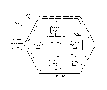
100601 As shown in FIG. 2A, in some variations, an analyte monitoring device
110 may
generally include a housing 112 and a microneedle array 140 extending
outwardly from the
housing. The housing 112, may, for example, be a wearable housing configured
to be worn on
the skin of a user such that the microneedle array 140 extends at least
partially into the skin of
the user. For example, the housing 112 may include an adhesive such that the
analyte monitoring
device 110 is a skin-adhered patch that is simple and straightforward for
application to a user.
The microneedle array 140 may be configured to puncture the skin of the user
and include one or
more electrochemical sensors (e.g., electrodes) configured for measuring one
or more target
analytes that are accessible after the microneedle array 140 punctures the
skin of the user. In
some variations, the analyte monitoring device 110 may be integrated or self-
contained as a
single unit, and the unit may be disposable (e.g., used for a period of time
and replaced with
another instance of the analyte monitoring device 110).
100611 An electronics system 120 may be at least partially arranged in the
housing 112 and
include various electronic components, such as sensor circuitry 124 configured
to perform signal
processing (e.g., biasing and readout of electrochemical sensors, converting
the analog signals
from the electrochemical sensors to digital signals, etc.). The electronics
system 120 may also
include at least one microcontroller 122 for controlling the analyte
monitoring device 110, at
least one communication module 126, at least one power source 130, and/or
other various
suitable passive circuitry 127. The microcontroller 122 may, for example, be
configured to
interpret digital signals output from the sensor circuitry 124 (e.g., by
executing a programmed
routine in firmware), perform various suitable algorithms or mathematical
transformations (e.g.,
calibration, etc.), and/or route processed data to and/or from the
communication module 124. In
some variations, the communication module 126 may include a suitable wireless
transceiver
(e.g., Bluetooth transceiver or the like) for communicating data with an
external computing
device 102 via one or more antennas 128. For example, the communication module
126 may be
9
CA 03163460 2022- 6- 29
WO 2022/026764
PCT/US2021/043786
configured to provide uni-directional and/or bi-directional communication of
data with an
external computing device 102 that is paired with the analyte monitoring
device 110. The power
source 130 may provide power for the analyte monitoring device 110, such as
for the electronics
system. The power source 130 may include battery or other suitable source, and
may, in some
variations, be rechargeable and/or replaceable. Passive circuitry 127 may
include various non-
powered electrical circuitry (e.g., resistors, capacitors, inductors, etc.)
providing
interconnections between other electronic components, etc. The passive
circuitry 127 may be
configured to perform noise reduction, biasing and/or other purposes, for
example. In some
variations, the electronic components in the electronics system 120 may be
arranged on one or
more printed circuit boards (PCB), which may be rigid, semi-rigid, or
flexible, for example.
Additional details of the electronics system 120 are described further below.
100621 In some variations, the analyte monitoring device 110 may further
include one or more
additional sensors 150 to provide additional information that may be relevant
for user
monitoring. For example, the analyte monitoring device 110 may further include
at least one
temperature sensor (e.g., thermistor) configured to measure skin temperature,
thereby enabling
temperature compensation for the sensor measurements obtained by the
microneedle array
electrochemical sensors.
100631 In some variations, the microneedle array 140 in the analyte monitoring
device 110
may be configured to puncture skin of a user. As shown in FIG. 2B, when the
device 110 is
worn by the user, the microneedle array 140 may extend into the skin of the
user such that
electrodes on distal regions of the microneedles rest in the dermis.
Specifically, in some
variations, the microneedles may be designed to penetrate the skin and access
the upper dermal
region (e.g., papillary dermis and upper reticular dermis layers) of the skin,
in order to enable the
electrodes to access interstitial fluid that surrounds the cells in these
layers. For example, in
some variations, the microneedles may have a height generally ranging between
at least 350 p.m
and about 515 pm. In some variations, one or more microneedles may extend from
the housing
such that a distal end of the electrode on the microneedle is located less
than about 5 mm from a
skin-interfacing surface of the housing, less than about 4 mm from the
housing, less than about 3
mm from the housing, less than about 2 mm from the housing, or less than about
1 mm from the
housing.
CA 03163460 2022- 6- 29
WO 2022/026764
PCT/US2021/043786
[0064] In contrast to traditional continuous analyte monitoring devices (e.g.,
CGM devices),
which include sensors typically implanted between about 8 mm and about 10 mm
beneath the
skin surface in the subcutis or adipose layer of the skin, the analyte
monitoring device 110 has a
shallower microneedle insertion depth of about 0.25 mm (such that electrodes
are implanted in
the upper dermal region of the skin) that provides numerous benefits. These
benefits include
access to dermal interstitial fluid including one or more target analytes for
detection, which is
advantageous at least because at least some types of analyte measurements of
dermal interstitial
fluid have been found to closely correlate to those of blood. For example, it
has been discovered
that glucose measurements performed using electrochemical sensors accessing
dermal interstitial
fluid are advantageously highly linearly correlated with blood glucose
measurements.
Accordingly, glucose measurements based on dermal interstitial fluid are
highly representative
of blood glucose measurements.
[0065]
Additionally, because of the shallower microneedle insertion depth of the
analyte
monitoring device 110, a reduced time delay in analyte detection is obtained
compared to
traditional continuous analyte monitoring devices. Such a shallower insertion
depth positions the
sensor surfaces in close proximity (e.g., within a few hundred micrometers or
less) to the dense
and well-perfused capillary bed of the reticular dermis, resulting in a
negligible diffusional lag
from the capillaries to the sensor surface. Diffusion time is related to
diffusion distance
according to t = x7(2D) where t is the diffusion time, x is the diffusion
distance, and D is the
mass diffusivity of the analyte of interest. Therefore, positioning an analyte
sensing element
twice as far away from the source of an analyte in a capillary will result in
a quadrupling of the
diffusional delay time. Accordingly, conventional analyte sensors, which
reside in the very
poorly vascularized adipose tissue beneath the dermis, result in a
significantly greater diffusion
distance from the vasculature in the dermis and thus a substantial diffusional
latency (e.g.,
typically 5 ¨ 20 minutes). In contrast, the shallower microneedle insertion
depth of the analyte
monitoring device 110 benefits from low diffusional latency from capillaries
to the sensor,
thereby reducing time delay in analyte detection and providing more accurate
results in real-time
or near real-time. For example, in some embodiments, diffusional latency may
be less than 10
minutes, less than 5 minutes, or less than 3 minutes.
[0066] Furthermore, when the microneedle array rests in the upper dermal
region, the lower
dermis beneath the microneedle array includes very high levels of
vascularization and perfusion
11
CA 03163460 2022- 6- 29
WO 2022/026764
PCT/US2021/043786
to support the dermal metabolism, which enables thermoregulation (via
vasoconstriction and/or
vasodilation) and provides a barrier function to help stabilize the sensing
environment around
the microneedles. Yet another advantage of the shallower insertion depth is
that the upper
dermal layers lack pain receptors, thus resulting in a reduced pain sensation
when the
microneedle array punctures the skin of the user, and providing for a more
comfortable,
minimally-invasive user experience.
100671 Thus, the analyte monitoring devices and methods described herein
enable improved
continuous monitoring of one or more target analytes of a user. For example,
as described above,
the analyte monitoring device may be simple and straightforward to apply,
which improves ease-
of-use and user compliance. Additionally, analyte measurements of dermal
interstitial fluid may
provide for highly accurate analyte detection. Furthermore, compared to
traditional continuous
analyte monitoring devices, insertion of the microneedle array and its sensors
may be less
invasive and involve less pain for the user. Additional advantages of other
aspects of the analyte
monitoring devices and methods are further described below.
Housing
100681 As described above, an analyte monitoring device may include a housing.
The housing
may at least partially surround or enclose other components of the analyte
monitoring device
(e.g., electronic components), such as for protection of such components. For
example, the
housing may be configured to help prevent dust and moisture from entering the
analyte
monitoring device. In some variations, an adhesive layer may attach the
housing to a surface
(e.g., skin) of a user, while permitting a microneedle array to extend
outwardly from the housing
and into the skin of the user. Furthermore, in some variations the housing may
generally include
rounded edges or corners and/or be low-profile so as to be atraumatic and
reduce interference
with clothing, etc worn by the user.
100691 For example, as shown in FIGS. 3A-3E, an example variation of an
analyte monitoring
device 300 may include a housing 310 configured to at least partially surround
other various
internal components of the device 300, and a microneedle array 330 that
extends outwardly from
a skin-facing surface (e.g., underside) of the housing 310.
12
CA 03163460 2022- 6- 29
WO 2022/026764
PCT/US2021/043786
[0070] The housing 310 may, for example, include one or more rigid or semi-
rigid protective
shell components that may couple together via suitable fasteners (e.g.,
mechanical fasteners),
mechanically interlocking or mating features, and/or an engineering fit. For
example, as shown
in FIG. 3E, the housing may include a housing cover 310a and a housing base
310b, where the
cover 310a and the base 310b may be secured together with one or more threaded
fasteners (e.g.,
fasteners that engage threaded holes in the upper and/or lower housing
portions). The cover 310a
and the base 310b may include radiused edges and corners, and/or other
atraumatic features.
When coupled together, the cover 310a and the base 310b may form an internal
volume that
houses other internal components such as a device printed circuit board 350
(PCB), a sensor
assembly 320, and/or other components such as a gasket 312. For example, the
internal
components arranged in the internal volume may be arranged in a compact, low
profile stack-up
as shown in FIG. 3E. While FIG. 3E illustrates a housing 310 include multiple
housing
components, in some variations the housing 310 may include a single component
defining the
internal volume for housing internal device components. In some embodiments,
the housing 310
may be filled with a suitable potting compound (e.g., epoxy) to reduce
deleterious environmental
effects such as temperature, humidity, pressure, and light.
100711 Furthermore, the analyte monitoring device 300 may include an adhesive
layer 340
configured to attach the housing 310 to a surface (e.g., skin) of a user. The
adhesive layer 340
may, for example, be attached to a skin-facing side of the housing 310 via a
double-sided
adhesive liner 344 as shown in in the variation depicted in FIG. 3D.
Alternatively, the adhesive
layer 340 may be coupled directly to the skin-facing side of the housing 310
with one or more
suitable fasteners (e.g., adhesive, mechanical fasteners, etc.). The adhesive
layer 340 may be
protected by a release liner that the user removes prior to skin application,
in order to expose the
adhesive. In some variations, the analyte monitoring device may include 3M
15O4XLTM
double-sided adhesive and 3M 4076 skin-facing adhesive, available from 3M .
These
materials are selected for their: breathability, wearability, mean water vapor
transmission rate
(MWVTR), biocompatibility, compatibility with sensor sterilization method /
strategy,
appearance, durability, tackiness, and ability to retain said tackiness for
the duration of sensor
wear.
100721 The adhesive layer 340 may, in some variations, have a perimeter that
extends farther
than the perimeter or periphery of the housing 310 (e.g., which may increase
surface area for
13
CA 03163460 2022- 6- 29
WO 2022/026764
PCT/US2021/043786
attachment and increase stability of retention, or the attachment to the skin
of a user).
Furthermore, in some variations, the adhesive layer 340 may include an opening
342 that
permits passage of the outwardly extending microneedle array 330. The opening
342 may
closely circumscribe the shape of the microneedle array 330 as shown in FIG.
3C (e.g., square
opening closely corresponding in size and shape to a square microneedle
array), or have another
suitable size and shape that is larger than the footprint area of the
microneedle array (e.g.,
circular opening larger than a square microneedle array).
100731 Although the housing 310 depicted in FIGS. 3A-3E is hexagonal shaped
and generally
prismatic, it should be understood that in other variations, the housing 310
may have any
suitable shape. For example, in other variations the housing may be generally
prismatic and have
a base that has an elliptical (e.g., circular), triangular, rectangular,
pentagonal, or other suitable
shape. As another example, FIGS. 4A-4C illustrate an example variation of an
analyte
monitoring device 400 including a dome-shaped housing 410. While the dome-
shaped housing
410 depicted in FIGS. 4A-4C is generally circular, in other variations the
dome-shaped housing
may have a base that has another suitable elliptical shape or polygonal shape.
100741 Similar to the housing 310, the housing 410 may include an internal
volume configured
to at least partially surround other components of the analyte monitoring
device 400. For
example, as shown in the cross-sectional view of FIG. 4D, the housing 410 may
include a domed
cover 410a coupled to a base 410b, so as to form an internal volume within
which a device PCB
450 and a sensor assembly with a microneedle array 430 may be arranged.
Additionally, the
housing 410 may be configured to couple to a surface via an adhesive layer
440, and the
microneedle array 430 may extend outwardly from the housing and beyond the
adhesive layer
440. Furthermore, as shown in FIGS. 4D and 4E, the adhesive layer 440 may
extend beyond the
perimeter of the housing 410.
User interface
100751 In some variations, an analyte monitoring system may provide user
status, analyte
monitoring device status, and/or other suitable information directly via a
user interface (e.g.,
display, indicator lights, etc. as described below) on the analyte monitoring
device. Thus, in
contrast to analyte monitoring systems that may solely communicate information
to a separate
peripheral device (e.g., mobile phone, etc.) that in turn communicates the
information to a user,
14
CA 03163460 2022- 6- 29
WO 2022/026764
PCT/US2021/043786
in some variations such information may be directly provided by the analyte
monitoring device.
Advantageously, in some variations, such a user interface on the analyte
monitoring device may
reduce the need for a user to constantly maintain a separate peripheral device
in order to monitor
user status and/or analyte monitoring device status (which may be impractical
due to cost,
inconvenience, etc.). Additionally, the user interface on the analyte
monitoring device may
reduce risks associated with loss of communication between the analyte
monitoring device and a
separate peripheral device, such as a user having an inaccurate understanding
of their current
analyte levels (e.g., leading the user to assume their analyte levels are high
when they are
actually low, which could, for example, result in the user self-administering
an inaccurate dose
of drug or withholding a therapeutic intervention when it is medically
necessary).
100761 Additionally, the ability to communicate information to a user via the
analyte
monitoring device itself, independently of a separate peripheral device, may
reduce or eliminate
the need to maintain compatibility between the analyte monitoring device and
separate
peripheral devices as such peripheral devices are upgraded (e.g., replaced
with new device
models or other hardware, run new versions of operating systems or other
software, etc.).
100771 Accordingly, in some variations, the housing may include a user
interface, such as an
interface to provide information in a visual, audible, and/or tactile manner
to provide
information regarding user status and/or status of the analyte monitoring
device, and/or other
suitable information. Examples of user status that may be communicated via the
user interface
include information representative of analyte measurement in the user (e.g.,
below a
predetermined target analyte measurement threshold or range, within a
predetermined target
analyte measurement range, above a predetermined target analyte measurement
threshold or
range, increase or decrease of analyte measurement over time, rate of change
of analyte
measurement, other information relating to trend of analyte measurements,
other suitable alerts
associated with analyte measurement, etc.). Examples of analyte monitoring
device status that
may be communicated via the user interface include device operation mode
(e.g., associated
with device warm-up state, analyte monitoring state, battery power status such
as low battery,
etc.), a device error state (e.g., operational error, pressure-induced sensing
attenuation, fault,
failure mode, etc.), device power status, device life status (e.g.,
anticipated sensor end-of-life),
status of connectivity between device and a mobile computing device, and/or
the like.
CA 03163460 2022- 6- 29
WO 2022/026764
PCT/US2021/043786
[0078] In some variations, the user interface may by default be in an enabled
or "on" state to
communicate such information at least whenever the analyte monitoring device
is performing
analyte measurements) or whenever the analyte monitoring device is powered on,
thereby
helping to ensure that information is continuously available to the user. For
example, user
interface elements may communicate through a display or indicator light(s)
(e.g., as described
below) not only alerts to flag user attention or recommend remedial action,
but also when user
status and/or device status are normal. Accordingly, in some variations, a
user is not required to
perform an action to initiate a scan to learn their current analyte
measurement level(s), and such
information may always readily be available to the user. In some variations,
however, a user
may perform an action to disable the user interface temporarily (e.g., similar
to a "snooze"
button) such as for a predetermined amount of time (e.g., 30 minutes, 1 hour,
2 hours, etc.) after
which the user interface is automatically reenabled, or until a second action
is performed to
reenable the user interface.
100791 In some variations, the user interface of the housing may include a
display configured
to visually communicate information. The display may, for example, include a
display screen
(e.g., LCD screen, OLED display, electrophoretic display, electrochromic
display, etc.)
configured to display alphanumeric text (e.g., numbers, letters, etc.),
symbols, and/or suitable
graphics to communicate information to the user. For example, the display
screen may include a
numerical information, textual information, and/or a graphics (e.g., sloped
line, arrows, etc.) of
information such as user status and/or status of the analyte monitoring
device. For example, the
display screen may include text or graphical representations of analyte
measurement levels,
trends, and/or recommendations (e.g., physical activity, reduced dietary
intake, etc.).
100801 As another example, the display on the housing may include one or more
indicator
lights (e.g., including LEDs, OLEDs, lasers, electroluminescent material, or
other suitable light
source, waveguides, etc.) that may be controlled in one or more predetermined
illumination
modes to communicate different statuses and/or other suitable information. An
indicator light
may be controlled to illuminate with multiple colors (e.g., red, orange,
yellow, green, blue,
and/or purple, etc.) or in only one color. For example, an indicator light may
include a multi-
colored LED. As another example, an indicator light may include a transparent
or semi-
transparent material (e.g., acrylic) positioned over one or more different-
colored light sources
(e.g., LED) such that different-colored light sources may be selectively
activated to illuminate
16
CA 03163460 2022- 6- 29
WO 2022/026764
PCT/US2021/043786
the indicator light in a selected color. The activation of light sources can
either occur
simultaneously or in sequence. An indicator light may have any suitable form
(e.g., raised, flush,
recessed, etc. from housing body) and/or shape (e.g., circle or other polygon,
ring, elongated
strip, etc.). In some variations, an indicator light may have a pinhole size
and/or shape to present
the same intensity of the light as a larger light source, but with
significantly less power
requirements, which may help conserve onboard power in the analyte monitoring
device.
100811 Indicator light(s) on the display may be illuminated in one or more
various manners to
communicate different kinds of information. For example, an indicator light
may be selectively
illuminated on or off to communicate information (e.g., illumination "on"
indicates one status,
while illumination "off' indicates another status). Additionally or
alternatively, an indicator light
may be illuminated in a selected color or intensity to communicate information
(e.g.,
illumination in a first color or intensity indicates a first status, while
illumination in a second
color or intensity indicates a second status). Additionally or alternatively,
an indicator light may
be illuminated in a selected temporal pattern to communicate information
(e.g., illumination in a
first temporal pattern indicates a first status, while illumination in a
second temporal pattern
indicates a second status). For example, an indicator light may be selectively
illuminated in one
of a plurality of predetermined temporal patterns that differ in illumination
frequency (e.g.,
repeated illumination at a rapid or slow frequency), regularity (e.g.,
periodic repeated
illumination vs. intermittent illumination), duration of illumination "on"
time, duration of
illumination "off' time, rate of change in illumination intensity, duty cycle
(e.g., ratio of
illumination "on- time to illumination "off' time), and/or the like, where
each predetermined
temporal pattern may indicate a respective status.
100821 Additionally or alternatively, in some variations, a display may
include multiple
indicator lights that may be collectively illuminated in one or more
predetermined illumination
modes or sequences in accordance with one or more predetermined spatial and/or
temporal
patterns. For example, in some variations, some or all of the indicator lights
arranged on a
display may be illuminated in synchrony or in sequence to indicate a
particular status.
Accordingly, the selected subset of indicator lights (e.g., the spatial
arrangement of the indicator
lights that are illuminated) and/or the manner in which they are illuminated
(e.g., illumination
order, illumination rate, etc.) may indicate a particular status. Additionally
or alternatively, a
plurality of indicator lights may illuminate simultaneously or in sequence to
increase the
17
CA 03163460 2022- 6- 29
WO 2022/026764
PCT/US2021/043786
diversity of the color palette. For example, in some variations, red, green,
and blue LEDs may be
illuminated in rapid succession to create the impression of white light to a
user.
100831 It should furthermore be understood that one or more of the above-
described
illumination modes may be combined in any suitable manner (e.g., combination
of varying
color, intensity, brightness, luminosity, contrast, timing, location, etc.) to
communicate
information. Additionally or alternatively, an ambient light sensor may be
incorporated into the
device body to enable dynamic adjustment light levels in the indicator
light(s) to compensate for
environmental light conditions to help conserve power. The ambient light
sensor may, in some
variations, be used in conjunction with a kinetic sensor (e.g., as described
in further detail
below) to further determine appropriate periods for the analyte monitoring
device to enter into a
power saving mode or reduced power state. For example, detection of darkness
and no motion of
the analyte monitoring device may indicate that the wearer of the analyte
monitoring device is
asleep, which may trigger the analyte monitoring device to enter into a power
saving mode or
reduced power state.
100841 FIG. 31A illustrates an example variation of an analyte monitoring
device 3 100
including a user interface 3120 with multiple indicator lights (3122, 3124a-
3124c). Indicator
light 3120 n-lay, for example, be selectively illuminated to indicate a device
state (e.g., operation
mode, error state, power status, life status, etc.). Although indicator light
3122 is in the shape of
a symbol (e.g., logo), it should be understood that in other variations, the
indicator light 3122
may have any suitable shape (e.g., text, other geometric shape, etc.).
Indicator lights 3124a-
3124c may be selectively illuminated to indicate a user status (e.g.,
information representative of
analyte measurement). Although indicator lights 3124a-3124c are linear
elements extending
across the user interface (e.g., chords across a circular display), it should
be understood that in
other variations, the indicator lights 3124a-3124c have other suitable shapes
(e.g., wavy lines,
circular, etc.). In some variations, a 1-dimensional array of indicator lights
of any suitable shape
may be arranged on the housing (e.g., arranged in a row, a column, an arc,
etc.). Alternatively,
the housing may include a multi-dimensional array of indicator lights of any
suitable shape.
100851 Furthermore, in some variations, an indicator light may include an icon
(e.g., symbol)
that may be indicative of analyte information (e.g., up arrow to indicate
rising analyte
measurement level trend, down arrow to indicate falling analyte measurement
level trend),
analyte monitoring device status (e.g., exclamation point to indicate a device
error state), and/or
18
CA 03163460 2022- 6- 29
WO 2022/026764
PCT/US2021/043786
other suitable information. Additionally or alternatively, iconography in the
indicator light(s)
may be used to communicate recommendations for the user such as behavioral
recommendations. Iconography may, for example, have the advantage of
communicating
recommendations to a user in a more universal or language-agnostic manner
(e.g., without the
need for language translations to tailor the device to different geographical
regions or user
preferences, etc.). For example, as shown in FIG. 31B, in some variations, in
the context of
glucose monitoring, a user interface for an analyte monitoring device 3100'
may include a
running person icon 3126 to indicate a recommendation that the user engage in
physical activity.
As another example, a food icon 3128 may indicate a recommendation that the
user consume
food (or in combination with an "X" icon 3130, to indicate a recommendation
that the user
restrict food). As another example, a drink icon 3132 may indicate a
recommendation that the
user consume fluid such as water (or in combination with an "X" icon 3134, to
indicate a
recommendation that the user restrict fluid). As another example, a star icon
3136 may indicate
positive reinforcement (e.g., indicating success in analyte measurement levels
staying within a
normal or target range for a predetermined period of time). However, it should
be understood
that behavioral recommendations may vary based on the indication relating to
the analyte(s)
being monitored. For example, in some variations in which the analyte
monitoring device is
additionally or alternatively used to monitor cortisol, rising cortisol levels
(and/or rising glucose
levels) may be correlated to an increase in user stress. Accordingly, in some
of these variations
the analyte monitoring device may include a suitable icon to indicate a
recommendation to the
user to reduce exposure to stressors, to meditate, etc. to avoid implicating
adverse health effects
due to stress.
[0086] In the variations shown in FIGS. 31A and 31B, each of the indicator
lights 3124a-
3124c may be exclusively illuminated to indicate a different analyte
measurement (e.g., in target
range, below target range, significantly below target range, above target
range, significantly
above target range, etc.). Furthermore, the indicator lights 3124a-3124c may
be arranged
adjacent to each other, such that they may be selectively illuminated in a
progressive sequence to
communicate trend information of analyte measurements (e.g., progressive
sequence of
illumination in a first direction that corresponds to an increase in measured
quantity of an
analyte, progressive sequence of illumination in a second direction that
corresponds to a
decrease in measured quantity of an analyte, pace of illumination progression
in the first
direction or the second direction that corresponds to a rate of increase or
decrease in measured
19
CA 03163460 2022- 6- 29
WO 2022/026764
PCT/US2021/043786
quantity of an analyte, etc.). An example of such progressive sequence of
illumination is further
described below with reference to FIGS. 33A-33D. While one device status
indicator light 3120
and three user status indicator lights 3124a-3124c are shown in FIGS. 31A and
31B, it should be
understood that in other variations, an analyte monitoring device may include
any suitable
number of indicator lights, such as one, two, three, four, five or more device
status indicator
lights, and one, two, three, four, five or more user status indicator lights.
Further details
regarding an example operation of the user interface 3120 to communicate
device status and/or
user status are described below (e.g., with reference to FIGS. 32A-32C, 33A-
33D, 34A-34C, and
35A-35B).
Microneedle array
100871 As shown in the schematic of FIG. 5A, in some variations, a microneedle
array 510 for
use in sensing one or more analytes may include one or more microneedles 510
projecting from
a substrate surface 502. The substrate surface 502 may, for example, be
generally planar and one
or more microneedles 510 may project orthogonally from the planar surface.
Generally, as
shown in FIG. 5B, a microneedle 510 may include a body portion 512 (e.g.,
shaft) and a tapered
distal portion 514 configured to puncture skin of a user. In some variations,
the tapered distal
portion 514 may terminate in an insulated distal apex 516. The microneedle 510
may further
include an electrode 520 on a surface of the tapered distal portion. In some
variations, electrode-
based measurements may be performed at the interface of the electrode and
interstitial fluid
located within the body (e.g., on an outer surface of the overall
microneedle). In some variations,
the microneedle 510 may have a solid core (e.g., solid body portion), though
in some variations
the microneedle 510 may include one or more lumens, which may be used for drug
delivery or
sampling of the dermal interstitial fluid, for example. Other microneedle
variations, such as
those described below, may similarly either include a solid core or one or
more lumens.
100881 The microneedle array 500 may be at least partially formed from a
semiconductor (e.g.,
silicon) substrate and include various material layers applied and shaped
using various suitable
microelectromechanical systems (MEMS) manufacturing techniques (e.g.,
deposition and
etching techniques), as further described below. The microneedle array may be
reflow-soldered
to a circuit board, similar to a typical integrated circuit. Furthermore, in
some variations the
microneedle array 500 may include a three electrode setup including a working
(sensing)
electrode having an electrochemical sensing coating (including a
biorecognition element such as
CA 03163460 2022- 6- 29
WO 2022/026764
PCT/US2021/043786
an enzyme) that enables detection of a target analyte, a reference electrode,
and a counter
electrode. In other words, the microneedle array 500 may include at least one
microneedle 510
that includes a working electrode, at least one microneedle 510 including a
reference electrode,
and at least one microneedle 510 including a counter electrode. Additional
details of these types
of electrodes are described in further detail below.
100891 In some variations, the microneedle array 500 may include a plurality
of microneedles
that are insulated such that the electrode on each microneedle in the
plurality of microneedles is
individually addressable and electrically isolated from every other electrode
on the microneedle
array. The resulting individual addressability of the microneedle array 500
may enable greater
control over each electrode's function, since each electrode may be separately
probed. For
example, the microneedle array 500 may be used to provide multiple independent
measurements
of a given target analyte, which improves the device's sensing reliability and
accuracy.
Furthermore, in some variations the electrodes of multiple microneedles may be
electrically
connected to produce augmented signal levels. As another example, the same
microneedle array
500 may additionally or alternatively be interrogated to simultaneously
measure multiple
analytes to provide a more comprehensive assessment of physiological status.
For example, as
shown in the schematic of FIG. 6, a microneedle array may include a portion of
microneedles to
detect a first Analyte A, a second portion of microneedles to detect a second
Analyte B, and a
third portion of microneedles to detect a third Analyte C. It should be
understood that the
microneedle array may be configured to detect any suitable number of analytes
(e.g., 1, 2, 3, 4, 5
or more, etc.). Suitable target analytes for detection may, for example,
include glucose, ketones,
lactate, and cortisol. For example, in some variations, ketones may be
detected in a manner
similar to that described in U.S. Patent App. No. 16/701,784, which is
incorporated herein in its
entirety by this reference. Thus, individual electrical addressability of the
microneedle array 500
provides greater control and flexibility over the sensing function of the
analyte monitoring
device.
100901 In some variations of microneedles (e.g., microneedles with a working
electrode), the
electrode 520 may be located proximal to the insulated distal apex 516 of the
microneedle. In
other words, in some variations the electrode 520 does not cover the apex of
the microneedle.
Rather, the electrode 520 may be offset from the apex or tip of the
microneedle. The electrode
520 being proximal to or offset from the insulated distal apex 516 of the
microneedle
21
CA 03163460 2022- 6- 29
WO 2022/026764
PCT/US2021/043786
advantageously provides more accurate sensor measurements. For example, this
arrangement
prevents concentration of the electric field at the microneedle apex 516
during manufacturing,
thereby avoiding non-uniform electro-deposition of sensing chemistry on the
electrode surface
520 that would result in faulty sensing.
100911 As another example, placing the electrode 520 offset from the
microneedle apex further
improves sensing accuracy by reducing undesirable signal artefacts and/or
erroneous sensor
readings caused by stress upon microneedle insertion. The distal apex of the
microneedle is the
first region to penetrate into the skin, and thus experiences the most stress
caused by the
mechanical shear phenomena accompanying the tearing or cutting of the skin. If
the electrode
520 were placed on the apex or tip of the microneedle, this mechanical stress
may del aminate the
electrochemical sensing coating on the electrode surface when the microneedle
is inserted,
and/or cause a small yet interfering amount of tissue to be transported onto
the active sensing
portion of the electrode. Thus, placing the electrode 520 sufficiently offset
from the microneedle
apex may improve sensing accuracy. For example, in some variations, a distal
edge of the
electrode 520 may be located at least about 10 nm (e.g., between about 20 nm
and about 30 nm)
from the distal apex or tip of the microneedle, as measured along a
longitudinal axis of the
microneedle.
100921 The body portion 512 of the microneedle 510 may further include an
electrically
conductive pathway extending between the electrode 520 and a backside
electrode or other
electrical contact (e.g., arranged on a backside of the substrate of the
microneedle array). The
backside electrode may be soldered to a circuit board, enabling electrical
communication with
the electrode 520 via the conductive pathway. For example, during use, the in-
vivo sensing
current (inside the dermis) measured at a working electrode is interrogated by
the backside
electrical contact, and the electrical connection between the backside
electrical contact and the
working electrode is facilitated by the conductive pathway. In some
variations, this conductive
pathway may be facilitated by a metal via running through the interior of the
microneedle body
portion (e.g., shaft) between the microneedle's proximal and distal ends.
Alternatively, in some
variations the conductive pathway may be provided by the entire body portion
being formed of a
conductive material (e.g., doped silicon). In some of these variations, the
complete substrate on
which the microneedle array 500 is built upon may be electrically conductive,
and each
microneedle 510 in the microneedle array 500 may be electrically isolated from
adjacent
22
CA 03163460 2022- 6- 29
WO 2022/026764
PCT/US2021/043786
microneedles 510 as described below. For example, in some variations, each
microneedle 510 in
the microneedle array 500 may be electrically isolated from adjacent
microneedles 510 with an
insulative barrier including electrically insulative material (e.g.,
dielectric material such as
silicon dioxide) that surrounds the conductive pathway extending between the
electrode 520 and
backside electrical contact. For example, body portion 512 may include an
insulative material
that forms a sheath around the conductive pathway, thereby preventing
electrical communication
between the conductive pathway and the substrate. Other example variations of
structures
enabling electrical isolation among microneedles are described in further
detail below.
[0093] Such electrical isolation among microneedles in the microneedle array
permits the
sensors to be individually addressable. This individually addressability
advantageously enables
independent and parallelized measurement among the sensors, as well as dynamic
reconfiguration of sensor assignment (e.g., to different analytes). In some
variations, the
electrodes in the microneedle array can be configured to provide redundant
analyte
measurements, which is an advantage over conventional analyte monitoring
devices. For
example, redundancy can improve performance by improving accuracy (e.g.,
averaging multiple
analyte measurement values for the same analyte which reduces the effect of
extreme high or
low sensor signals on the determination of analyte levels) and/or improving
reliability of the
device by reducing the likelihood of total failure.
[0094] In some variations, as described in further detail below with
respective different
variations of the microneedle, the microneedle array may be formed at least in
part with suitable
semiconductor and/or MEMS fabrication techniques and/or mechanical cutting or
dicing. Such
processes may, for example, be advantageous for enabling large-scale, cost-
efficient
manufacturing of microneedle arrays. For example, in some variations, the
microneedle array
may be formed at least in part using techniques described in U.S. Patent App.
No. 15/913,709,
which is incorporated herein in its entirety by this reference.
Microneedle structures
100951 Described herein are multiple example variations of microneedle
structure
incorporating one or more of the above-described microneedle features for a
microneedle array
in an analyte monitoring device.
23
CA 03163460 2022- 6- 29
WO 2022/026764
PCT/US2021/043786
[0096] In some variations, a microneedle may have a generally columnar body
portion and a
tapered distal portion with an electrode. For example, FIGS. 7A-7C illustrate
an example
variation of a microneedle 700 extending from a substrate 702. FIG. 7A is a
side cross-sectional
view of a schematic of microneedle 700, while FIG. 7B is a perspective view of
the microneedle
700 and FIG. 7C is a detailed perspective view of a distal portion of the
microneedle 700. As
shown in FIGS. 7B and 7C, the microneedle 700 may include a columnar body
portion 712, a
tapered distal portion 714 terminating in an insulated distal apex 716, and an
annular electrode
720 that includes a conductive material (e.g., Pt, Ir, Au, Ti, Cr, Ni, etc.)
and is arranged on the
tapered distal portion 714. As shown in FIG. 7A, the annular electrode 720 may
be proximal to
(or offset or spaced apart from) the distal apex 716. For example, the
electrode 720 may be
electrically isolated from the distal apex 716 by a distal insulating surface
715a including an
insulating material (e.g., SiO2). In some variations, the electrode 720 may
also be electrically
isolated from the columnar body portion 712 by a second distal insulating
surface 715b. The
electrode 720 may be in electrical communication with a conductive core 740
(e.g., conductive
pathway) passing along the body portion 712 to a backside electrical contact
730 (e.g., made of
Ni/Au alloy) or other electrical pad in or on the substrate 702. For example,
the body portion 712
may include a conductive core material (e.g., highly doped silicon). As shown
in FIG. 7A, in
some variations, an insulating moat 713 including an insulating material
(e.g., SiO2) may be
arranged around (e.g., around the perimeter) of the body portion 712 and
extend at least partially
through the substrate 702. Accordingly, the insulating moat 713 may, for
example, help prevent
electrical contact between the conductive core 740 and the surrounding
substrate 702. The
insulating moat 713 may further extend over the surface of the body portion
712. Upper and/or
lower surfaces of the substrate 702 may also include a layer of substrate
insulation 704 (e.g.,
SiO2). Accordingly, the insulation provided by the insulating moat 713 and/or
substrate
insulation 704 may contribute at least in part to the electrical isolation of
the microneedle 700
that enables individual addressability of the microneedle 700 within a
microneedle array.
Furthermore, in some variations the insulating moat 713 extending over the
surface of the body
portion 712 may function to increase the mechanical strength of the
microneedle 700 structure.
[0097] The microneedle 700 may be formed at least in part by suitable MEMS
fabrication
techniques such as plasma etching, also called dry etching. For example, in
some variations, the
insulating moat 713 around the body portion 712 of the microneedle may be made
by first
forming a trench in a silicon substrate by deep reactive ion etching (1)1t1E)
from the backside of
24
CA 03163460 2022- 6- 29
WO 2022/026764
PCT/US2021/043786
the substrate, then filling that trench with a sandwich structure of SiO2 /
polycrystalline silicon
(poly-Si) / SiO2 by low pressure chemical vapor deposition (LPCVD) or other
suitable process.
In other words, the insulating moat 713 may passivate the surface of the body
portion 712 of the
microneedle, and continue as a buried feature in the substrate 702 near the
proximal portion of
the microneedle. By including largely compounds of silicon, the insulating
moat 713 may
provide good fill and adhesion to the adjoining silicon walls (e.g., of the
conductive core 740,
substrate 702, etc.). The sandwich structure of the insulating moat 713 may
further help provide
excellent matching of coefficient of thermal expansion (CTE) with the adjacent
silicon, thereby
advantageously reducing faults, cracks, and/or other thermally-induced
weaknesses in the
insulating structure 713.
100981 The tapered distal portion may be fashioned out by an isotropic dry
etch from the
frontside of the substrate, and the body portion 712 of the microneedle 700
may be formed from
DRIE. The frontside metal electrode 720 may be deposited and patterned on the
distal portion by
specialized lithography (e.g., electron-beam evaporation) that permits metal
deposition in the
desired annular region for the electrode 720 without coating the distal apex
716. Furthermore,
the backside electrical contact 730 of Ni/Au may be deposited by suitable MEMS
manufacturing
techniques (e.g., sputtering).
100991 The microneedle 700 may have any suitable dimensions. By way of
illustration, the
microneedle 700 may, in some variations, have a height of between about 300 pm
and about 500
pm. In some variations, the tapered distal portion 714 may have a tip angle
between about 60
degrees and about 80 degrees, and an apex diameter of between about 1 gm and
about 15 pm. In
some variations, the surface area of the annular electrode 720 may include
between about 9,000
1.1m2 and about 11,000 p.m2, or about 10,000 m2. FIG. 8 illustrates various
dimensions of an
example variation of a columnar microneedle with a tapered distal portion and
annular electrode,
similar to microneedle 700 described above.
101001 FIG. 9 illustrates another example variation of a microneedle 900
having a generally
columnar body portion. The microneedle 900 may be similar to microneedle 700
as described
above, except as described below. For example, like the microneedle 700, the
microneedle 900
may include a columnar body portion 912, and a tapered distal portion 914
terminating in an
insulated distal apex 916. The microneedle 900 may further include an annular
electrode 920
that includes a conductive material and is arranged on the tapered distal
portion 914 at a location
CA 03163460 2022- 6- 29
WO 2022/026764
PCT/US2021/043786
proximal to (or offset from or spaced apart from) the distal apex 916. Other
elements of
microneedle 900 have numbering similar to corresponding elements of
microneedle 700.
101011 However, compared to the microneedle 700, the microneedle 900 may have
a sharper
tip at the distal apex 916 and a modified insulating moat 913. For example,
the distal apex 916
may have a sharper tip angle, such as between about 25 degrees and about 45
degrees, and an
apex radius of less than about 100 nm, which provides a sharper microneedle
profile that may
penetrate skin with greater ease, lower velocity, less energy, and/or less
trauma. Furthermore, in
contrast to the insulating moat 713 (which extends through the substrate 702
and along the
height of the microneedle body portion 712 as shown in FIG. 7A), the modified
insulating moat
913 may extend only through the substrate 902 such that the sandwich structure
filling the trench
(e.g., created by DRIE as described above) forms only the buried feature in
the substrate.
Although the sidewall of the microneedle 900 is shown in FIG. 9 as extending
generally
orthogonal to the substrate surface, it should be understood that because the
modified insulating
moat 913 need not extend the entire height of the microneedle body portion
712, in some
variations the sidewall of the microneedle 900 may be angled at non-orthogonal
angles relative
to the substrate (e.g., the sidewall may have a slight positive taper of
between about 1 degree to
about 10 degrees, or between about 5 degrees and about 10 degrees).
101021 In some variations, the rest of the microneedle surface 900 (aside from
the annular
electrode 920) may include an insulating material extending from substrate
insulation 904. For
example, a layer of an insulating material (e.g., SiO2) may extend from a
frontside surface of the
substrate 902 to provide a body portion insulation 918, and may further extend
up over a
proximal edge of the electrode 920 as shown in FIG. 9. Another region of
insulating material
may similarly cover a distal edge of the electrode 920 and insulate the distal
apex 916. Such
region of insulating material and/or modified insulating moat 913 may help
prevent electrical
contact between the conductive core 940 and the surrounding substrate 902.
Accordingly, like
the microneedle 700, the microneedle 900 may maintain electrical isolation for
individual
addressability within a microneedle array. In some variations, the process to
form microneedle
900 may result in higher yield and/or provide lower production cost compared
to the process to
form microneedle 700.
101031 The microneedle 900 may have any suitable dimensions. By way of
illustration, the
microneedle 900 may, in some variations, include a height of between about 400
gm and about
26
CA 03163460 2022- 6- 29
WO 2022/026764
PCT/US2021/043786
600 gm, or about 500 gm. In some variations, the tapered distal portion 914
may have a tip
angle of between about 25 degrees and about 45 degrees, with a tip radius of
less than about 100
nm. Furthermore, the microneedle may have a shaft diameter of between about
160 p.m and
about 200 gm. FIG. 10 illustrates additional various dimensions of an example
variation of a
columnar microneedle with a tapered distal portion and annular electrode,
similar to microneedle
900 described above.
101041 FIGS. 27A-27F illustrate another example variation of a microneedle
2700 having a
generally columnar body portion. The microneedle 2700 may be similar to
microneedle 700 as
described above, except as described below. For example, as shown in FIG. 27B,
like the
microneedle 700, the microneedle 2700 may include a columnar body portion
2712, and a
tapered distal portion arranged on a cylinder 2713 and terminating in an
insulated distal apex
2716. The cylinder 2613 may be insulated and have a smaller diameter than the
columnar body
portion 2712. The microneedle 2700 may further include an annular electrode
2720 that includes
a conductive material and is arranged on the tapered distal portion at a
location proximal to (or
offset or spaced apart from) the distal apex 2916. Other elements of
microneedle 2700 as shown
in FIGS. 27A-27F have numbering similar to corresponding elements of
microneedle 700.
101051 However, the electrode 2720 on the microneedle 2700 may include a tip
contact trench
2722. This contact trench may be configured to help establish ohmic contact
between the
electrode 2720 and the underlying conductive core 2740 of the microneedle. In
some variations,
the shape of the tip contact trench 2722 may include an annular recess formed
in the surface of
the conductive core 2740 (e.g., into the body portion of the microneedle, or
otherwise in contact
with a conductive pathway in the body portion) such that when the electrode
2720 material is
deposited onto the conductive core 2740, the electrode 2720 with the tip
contact trench 2722
may have a stepped profile when viewed from the side. The tip contact trench
2722 may
advantageously help provide a margin of error to ensure contact between the
electrode 2720 and
the underlying conductive core 2740. Any of the other microneedle variations
described herein
may also have a similar tip contact trench to help ensure contact between the
electrode (which
may be, for example, a working electrode, reference electrode, counter
electrode, etc.) with a
conductive pathway within the microneedle.
101061 FIGS. 28A and 28B illustrate additional various dimensions of an
example variation of
a columnar microneedle with a tapered distal portion and annular electrode,
similar to
27
CA 03163460 2022- 6- 29
WO 2022/026764
PCT/US2021/043786
microneedle 2700 described above. For example, the variation of the
microneedle shown in
FIGS. 28A and 28B may have a tapered distal portion generally having a taper
angle of about 80
degrees (or between about 78 degrees and about 82 degrees, or between about 75
degrees and
about 85 degrees), and a cone diameter of about 140 gm (or between about 133
gm and about
147 gm, or between about 130 gm and about 150 gm). The cone of the tapered
distal portion
may be arranged on a cylinder such that the overall combined height of the
cone and cylinder is
about 110 gm (or between about 99 gm and about 116 gm, or between about 95 gm
and about
120 p[m). The annular electrode on the tapered distal portion may have an
outer or base diameter
of about 106 gm (or between about 95 gm and about 117 gm, or between about 90
gm and
about 120 gm), and an inner diameter of about 33.2 um (or between about 30 pm
and about 36
gm, or between about 25 gm and about 40 gm). The length of the annular
electrode, as
measured along the slope of the tapered distal portion, may be about 57 gm (or
between about
55 gm and about 65 gm), and the overall surface area of the electrode may be
about 12,700 gm'
(or between about 12,500 gm2 and about 12,900 um2, or between about 12,000
p.m2 and about
13,000 gm2). As shown in FIG. 28B, the electrode may furthermore have a tip
contact trench
extending around a central region of the cone of the tapered distal portion,
where the contact
may have a width of about 11 pm (or between about 5 gm and about 50 jim,
between about 10
gm and about 12 gm, or between about 8 gm and about 14 gm) as measured along
the slope of
the tapered distal portion, and a trench depth of about 1.5 gm (or between
about 0.1 gm and
about 5 jim, or between about 0.5 gm and about 1.5 jim, or between about 1.4
p.m and about
1.6 gm, or between about 1 gm and about 2 gm). The microneedle has an
insulated distal apex
having a diameter of about 5.5 gm (or between about 5.3 gm and about 5.8 gm,
or between
about 5 gm and about 6 gm).
101071 In some variations, a microneedle may have a generally pyramidal body
portion and a
tapered distal portion with an electrode. For example, FIG. 11A illustrates an
example variation
of a microneedle 1100 having a generally pyramidal body portion 1112 and a
tapered distal
portion 1114 extending from the body portion 1112. The microneedle 1100 may
also include an
annular electrode 1120 arranged on the tapered distal portion 1114 and
proximal to an insulated
distal apex 1116. The electrode 1120 may be conductively coupled via a
conductive pathway
through the conductive core 1140 of the microneedle to a backside electrical
contact 1130. Like
the microneedle 900 described above with respect to FIG. 9, the microneedle
1100 may include
an insulating moat 1113 that is arranged around the base of the body portion
1112 and extends
28
CA 03163460 2022- 6- 29
WO 2022/026764
PCT/US2021/043786
through the substrate 1102 to provide electrical insulation around the
microneedle 1100 (e.g., for
individual addressability) and help prevent electrical contact between the
conductive core 1140
and the surrounding substrate 1102. However, in contrast to the insulating
moat 913 shown in
FIG. 9, the insulating moat 1113 may be offset from the base of the
microneedle 1100. The moat
may, for example, be offset between about 10 pm and about 400 pm, between
about 10 pm and
about 300 pm, between about 10 pm and about 200 pm, or between about 10 pm and
about 100
pm from where the base of the microneedle 1100 meets the substrate 1102 to
which it is
attached. In some variations, the insulating moat may include a filler
material including
parylene, Si-IN4, and SiO2, which may provide for low thermal stress and an
insulating material
that is chemical- and water-resistant. Additional body portion insulation 1118
may extend from a
frontsi de surface of the substrate 1102 up to the proximal edge of the
electrode 1120. Another
region of insulating material may extend from the distal edge of the electrode
1120 and insulate
the distal apex 1116.
101081 As shown in FIG. 11B, in some variations a microneedle 1100 having a
pyramidal
body portion 1112 may include a polygonal base, though the base may have any
suitable shape
(e.g., circular). The pyramidal body portion 1112 may include a plurality of
planar facets each
extending from a respective of the polygonal base of the microneedle. In some
variations, the
planar facets may include anisotropically etched <311> planar facets for
increased mechanical
strength (e.g., compressive strength and shear strength) of the microneedle
1110 and/or
increased electrode surface area relative to a circular cone with a non-planar
faceted surface. For
example, the microneedle 1110 may have an octagonal base with anisotropically
etched <311>
planar facets that increase the mechanical strength and increase the
metallization surface of the
microneedle 110 for the electrode surface
101091 The microneedle 1100 may be formed at least in part by suitable MEMS
fabrication
techniques. For example, the microneedle pyramidal structure may be formed by
a timed
anisotropic wet etch of a silicon wafer substrate. To form the annular
electrode surface, metal
deposition on the tapered distal portion of the microneedle may be performed,
such as using
specialized lithographic techniques as described above with respect to
electrode 720, without
coating the distal apex 1116. However, compared to the process described above
to form
microneedle 700, much of the process to form microneedle 1100 does not involve
expensive RIE
techniques, which may thereby substantially reduce manufacturing costs.
Furthermore, in some
29
CA 03163460 2022- 6- 29
WO 2022/026764
PCT/US2021/043786
variations, instead of utilizing dry etch processes as described above with
respect to microneedle
700, a process of forming the microneedle 1100 may include mechanical dicing,
bulk
micromachining, or other cutting techniques to shape the microneedle 1100 into
having a
pyramidal body. Furthermore, such techniques may be performed at a large
scale, so as to form,
for example, multiple microneedles 1110 arranged in an array as shown in FIG.
11C.
101101 The microneedle 1100 may have any suitable dimensions. By way of
illustration, the
microneedle 1100 may, in some variations, have a height of between about 400
um and about
600 um, or about 500 um. In some variations, the tapered distal portion 714
may have a tip
angle between about 30 degrees and about 50 degrees, or about 40 degrees,
which may provide a
good balance between sharpness for skin penetration and lithography
processability on the
sloped surface on which the electrode 1120 is to be disposed.
101111 FIG. 12 illustrates various dimensions of an example variation of a
pyramidal
microneedle with a tapered distal portion having planar facets and an
electrode arranged on at
least a portion of the planar facets. While in some variations the electrode
may be annular or
annular-like in that all of the planar facets on the pyramidal microneedle may
include a
metallization surface for the electrode, it should be understood that
alternatively, in some
variations only a portion of the planar facets on the pyramidal microneedle
may include a
metallization surface (e.g., one, two, three, four, five, six, or seven planar
facets of a pyramidal
microneedle having an octagonal base and eight planar facets extending
distally from the
octagonal base).
101121 In some variations, a pyramidal microneedle may be similar to that
described above
with respect to FIG. 11A, except that the microneedle may have an asymmetrical
shape as
shown in FIGS. 13A and 13B. For example, in some variations as shown in FIG.
13A, a
microneedle 1300 may have a non-circular or polygonal (e.g., square,
octagonal) base, but may
taper in a radially asymmetric manner. For example, the microneedle 1300 may
include at least
one cut surface 1350 (e.g., planar surface) that is offset from the distal
apex 1316 of the
microneedle (that is, not extending through a central z-axis defined as
passing from the base of
the microneedle 1300 to the distal apex 1316. The insulated distal apex 1316
may be kept intact
so as to not compromise surface area for metallization for the electrode. In
some variations, the
cut surface 1350 may be angled at a non-orthogonal angle relative to the base
of the microneedle
(and/or surface of the substrate 1302), as shown in FIG. 13A. For example, in
some variations
CA 03163460 2022- 6- 29
WO 2022/026764
PCT/US2021/043786
the cut surface may configured to produce a sharpened asymmetrical distal tip
at distal apex
1316 that is less than about 50 degrees, less than 40 degrees, less than about
30 degrees, or less
than about 20 degrees. Alternatively, in some variations the cut surface 1350
may be angled
normal to or orthogonal to the base of the microneedle (and/or surface of the
substrate 1302).
101131 Additionally or alternatively, as shown in FIG. 13A, an example
variation of an
asymmetric microneedle 1300 may have a polygonal (e.g., octagonal) base, but
include various
sloped surfaces that taper at different angles. As shown in FIG. 13A, a body
portion 1316 of the
microneedle 1300 may have a first taper angle (A) and a second taper angle (B)
measured
relative to a base of the body portion (and/or surface of the substrate 1302).
The second taper
angle (B) may be greater than the first taper angle (A) such that the
microneedle has a sharper
penetrating tip extending from a stable, mechanically strong base. For
example, in some
variations, the first taper angle (A) may be between about 10 degrees and
about 30 degrees,
between about 15 degrees and about 25 degrees, or about 20 degrees.
Additionally, in some
variations, the second taper angle (B) may be between about 60 degrees and
about 80 degrees,
between about 65 degrees and about 75 degrees, or about 70 degrees.
101141 FIGS. 13C-13E depict a series of steps in an example variation of
forming a pyramidal
microneedle with an asymmetric cut surface. As shown in FIG. 13C, a symmetric
pyramidal
microneedle with two taper angles may be formed through an anisotropic wet
etch process. The
two taper angles of the microneedle may include, for example, a first taper
angle of about 20
degrees located near the base of the microneedle, and a second taper angle of
about 70 degrees
located distal to the first tape angle, thereby forming progressively sloping
surfaces (e.g., along
planar facets of the pyramidal microneedle). As shown in FIG. 13D, a dicing
blade may be
applied at an angle offset from the distal apex of the microneedle, so as to
form a cut surface
similar to cut surface 1350 described above. The cut surface may leave a
reduced microneedle
base diameter (e.g., between about 150 lam and about 190 tm, or about 170 gm)
so as to result
in low tissue trauma. As shown in FIG. 13E, the resulting microneedle (with
its offset cut
surface) is asymmetric but has an intact, sharp distal apex.
101151 Like the pyramidal microneedle 1100 described above with respect to
FIG. 11A, the
microneedle 1300 may derive its mechanical strength at least in part from
anisotropically etched
<311> planes and the pyramidal shape. However, an asymmetric pyramidal
microneedle with a
asymmetric cut surface may be advantageous in that it may reduce the
longitudinal shear forces
31
CA 03163460 2022- 6- 29
WO 2022/026764
PCT/US2021/043786
compared to a symmetric microneedle having similar dimensions but lacking the
asymmetric
cut. Furthermore, a sharper (e.g., more acute angle) distal microneedle tip
may be achieved with
such an asymmetric cut surface. Although the cut surface 1350 is shown in FIG.
13A as
positioned at a non-orthogonal angle relative to the base of the microneedle,
alternatively as
described above, in some variations the cut surface 1350 may be generally
orthogonal or normal
to the base of the microneedle (and/or surface of the substrate 1302), which
may further reduce
the longitudinal shear forces in the microneedle.
[0116] In some variations, a microneedle may be similar to those described
above, except that
the microneedle may include a columnar body portion and a pyramidal distal
portion. For
example, as shown in FIG. 14A, a columnar-pyramidal microneedle 1400 may
include a
columnar body portion 1412 that may extend from a polygonal (e.g., octagonal)
base out of a
non-electrically conductive substrate 1402 such as intrinsic (undoped)
silicon. Additionally, the
columnar-pyramidal microneedle 1400 may include a tapered distal portion 1414
having a
pyramidal shape with a plurality of planar facets For example, the columnar-
pyramidal
microneedle 1400 may include a tapered distal portion 1414 having a pyramidal
shape with eight
facets extending from the octagonal columnar body portion 1412. However, the
pyramidal shape
may have any suitable number of planar facets (e.g., one, two, three, four,
five, six, seven, nine,
or more). An annular electrode 1420 may be formed on all the planar facets of
the pyramidal
distal portion 1414, or on only a portion of the planar facets (e.g., on one,
two, three, four, five,
six, seven facets) may include a metallization surface for the electrode.
Similar to that described
above, the columnar body portion 1412 may include a conductive core including
an electrically
conductive material functioning as a conductive pathway for signals to and
from the electrode
142. The columnar body portion 1412 may further include an insulation material
1418 may
extend along the body portion 1412 and up to (or slightly overlapping) a
proximal edge of the
electrode 1420. The distal apex 1416 may or may not be covered by similar
insulation material.
[0117] In some variations, the tapered distal portion 1414 may be similar to
that described
above with respect to FIGS. 11A-11C, 12, and/or 13A-13E. For example, the
tapered distal
portion 1414 may be formed using anisotropic wet etching techniques. The
electrode 1420 may
be formed on the tapered distal portion 1414 by lithography, electrodeposition
or other suitable
technique. The tapered distal portion 1414 may then be protected by an etch
resistant material
32
CA 03163460 2022- 6- 29
WO 2022/026764
PCT/US2021/043786
while the body portion 1412 is formed out of the substrate by dry etching
(e.g., DRIE) or other
suitable process(es).
101181 The combination of columnar and pyramidal aspects of the microneedle
1400 has a
number of advantages. Similar to that described above, the tapered distal
portion 1414 and apex
1416 have high mechanical strength due to the <311> wet etched planes and the
pyramidal
shape. Additionally, because the substrate is formed from a non-conductive
material, an
insulation "moat" as described above may not be required to electrically
isolate the microneedle,
thereby simplifying and reducing cost of fabrication. The absence of the
insulation moat also
permits material continuity in the substrate, which may lead to better
mechanical integrity of the
overall microneedle array structure.
101191 Although the columnar-pyramidal microneedle 1400 is described above as
including a
non-conductive substrate, it should be understood alternatively, in some
variations a columnar-
pyramidal microneedle may include a conductive core extending from a
conductive substrate
(e.g., doped silicon). For example, in some variations the columnar body
portion 1412 may be
similar to that described above with respect to FIGS. 7A-7C, and 8-10 (e.g.,
may include an
insulation moat to electrically isolate the microneedle, etc.).
101201 In some variations of microneedle arrays including one or more
microneedles 1400,
conductive pathways may be formed in the non-conductive substrate to
facilitate communication
with the electrode(s) 1420. For example, as described above, the body portion
1412 of each
microneedle may include a conductive core including a conductive material.
Such conductive
material may extend between the electrode 1420 to the substrate 1402. As shown
in FIG. 15D,
the microneedle array may include one or more connectors 1510 made of a
conductive material
(e.g., gold, aluminum) that is each in turn coupled to a backside electrical
contact 1530 for
further sensor communication. In some variations, as shown FIGS. 15A-15D, the
one or more
connectors 1510 may extend laterally along the surface of the substrate and
then connect to the
backside electrical contact 1530 with a conductive via 1520 within the
substrate.
101211 Additional details of example variations of microneedle array
configurations are
described in further detail below.
33
CA 03163460 2022- 6- 29
WO 2022/026764
PCT/US2021/043786
Electrodes
101221 As described above, each microneedle in the microneedle array may
include an
electrode. In some variations, multiple distinct types of electrodes may be
included among the
microneedles in the microneedle array. For example, in some variations the
microneedle array
may function as an electrochemical cell operable in an electrolytic manner
with three types of
electrodes. In other words, the microneedle array may include at least one
working electrode, at
least one counter electrode, and at least one reference electrode. Thus, the
microneedle array
may include three distinct electrode types, though one or more of each
electrode type may form
a complete system (e.g., the system might include multiple distinct working
electrodes).
Furthermore, multiple distinct microneedles may be electrically joined to form
an effective
electrode type (e.g., a single working electrode may be formed from two or
more connected
microneedles with working electrode sites). Each of these electrode types may
include a
metallization layer and may include one or more coatings or layers over the
metallization layer
that help facilitate the function of that electrode.
101231 Generally, the working electrode is the electrode at which oxidation
and/or reduction
reaction of interest occurs for detection of an analyte of interest. The
counter electrode functions
to source (provide) or sink (accumulate) the electrons, via an electrical
current, that are required
to sustain the electrochemical reaction at the working electrode. The
reference electrode
functions to provide a reference potential for the system; that is, the
electrical potential at which
the working electrode is biased is referenced to the reference electrode. A
fixed, time-varying, or
at least controlled potential relationship is established between the working
and reference
electrodes, and within practical limits no current is sourced from or sinked
to the reference
electrode. Additionally, to implement such a three-electrode system, the
analyte monitoring
device may include a suitable potentiostat or electrochemical analog front end
to maintain a
fixed potential relationship between the working electrode and reference
electrode contingents
within the electrochemical system (via an electronic feedback mechanism),
while permitting the
counter electrode to dynamically swing to potentials required to sustain the
redox reaction of
interest.
34
CA 03163460 2022- 6- 29
WO 2022/026764
PCT/US2021/043786
Working electrode
101241 As described above, the working electrode is the electrode at which the
oxidation
and/or reduction reaction of interest occurs. In some variations, sensing may
be performed at the
interface of the working electrode and interstitial fluid located within the
body (e.g., on an outer
surface of the overall microneedle). In some variations, a working electrode
may include an
electrode material and a biorecognition layer in which a biorecognition
element (e.g., enzyme) is
immobilized on the working electrode to facilitate selective analyte
quantification. In some
variations, the biorecognition layer may also function as an interference-
blocking layer and may
help prevent endogenous and/or exogenous species from directly oxidizing (or
reducing) at the
electrode.
101251 A redox current detected at the working electrode may be correlated to
a detected
concentration of an analyte of interest. This is because assuming a steady-
state, diffusion-limited
system, the redox current detected at the working electrode follows the
Cottrell relation below:
nF A\15 C
i(t) = _______________________________________________
V7rt
where n is the stoichiometric number of electrons mitigating a redox reaction,
F is Faraday's
constant, A is electrode surface area, D is the diffusion coefficient of the
analyte of interest, C is
the concentration of the analyte of interest, and t is the duration of time
that the system is biased
with an electrical potential. Thus, the detected current at the working
electrode scales linearly
with the analyte concentration.
101261 Moreover, because the detected current is a direct function of
electrode surface area A,
the surface area of the electrode may be increased to enhance the sensitivity
(e.g., amperes per
molar of analyte) of the sensor. For example, multiple singular working
electrodes may be
grouped into arrays of two or more constituents to increase total effective
sensing surface area.
Additionally or alternatively, to obtain redundancy, multiple working
electrodes may be
operated as parallelized sensors to obtain a plurality of independent measures
of the
concentration of an analyte of interest. The working electrode can either be
operated as the
anode (such that an analyte is oxidized at its surface), or as the cathode
(such that an analyte is
reduced at its surface).
CA 03163460 2022- 6- 29
WO 2022/026764
PCT/US2021/043786
[0127] FIG. 16A depicts a schematic of an exemplary set of layers for a
working electrode
1610. For example, as described above, in some variations the working
electrode 1610 may
include an electrode material 1612 and a biorecognition layer including a
biorecognition
element. The electrode material 1612 functions to encourage the
electrocatalytic detection of an
analyte or the product of the reaction of the analyte and the biorecognition
element. The
electrode material 1612 also provides ohmic contact and routes an electrical
signal from the
electrocatalytic reaction to processing circuitry. In some variations, the
electrode material 1612
may include platinum as shown in FIG. 16A. However, the electrode material
1612 may
alternatively include, for example, palladium, iridium, rhodium, gold,
ruthenium, titanium,
nickel, carbon, doped diamond, or other suitable catalytic and inert material.
[0128] In some variations, the electrode material 1612 may be coated with a
highly porous
electrocatalytic layer, such as a platinum black layer 1613, which may augment
the electrode
surface area for enhanced sensitivity. Additionally or alternatively, the
platinum black layer
1613 may enable the electrocatalytic oxidation or reduction of the product of
the biorecognition
reaction facilitated by the biorecognition layer 1614. However, in some
variations the platinum
black layer 1613 may be omitted (as shown in FIGS. 16D and 16G, for example).
The electrode
may enable the electrocatalytic oxidation or reduction of the product of the
biorecognition
reaction if the platinum black layer 1613 is not present.
[0129] The biorecognition layer 1614 may be arranged over the electrode
material 1612 (or
platinum black layer 1613 if it is present) and functions to immobilize and
stabilize the
biorecognition element which facilitates selective analyte quantification for
extended time
periods. In some variations, the biorecognition element may include an enzyme,
such as an
oxidase. As an exemplary variation for use in a glucose monitoring system, the
biorecognition
element may include glucose oxidase, which converts glucose, in the presence
of oxygen, to an
electroactive product (i.e., hydrogen peroxide) that can be detected at the
electrode surface.
Specifically, the redox equation associated with this exemplary variation is
Glucose + Oxygen
Hydrogen Peroxide + Gluconolactone (mediated by glucose oxidase), Hydrogen
Peroxide
Water + Oxygen (mediated by applying an oxidizing potential at the working
electrode).
[0130] However, in other variations the biorecognition element may
additionally or
alternatively comprise another suitable oxidase or oxidoreductase enzyme such
as lactate
oxidase, alcohol oxidase, beta-hydroxybutyrate dehydrogenase, tyrosinase,
catalase, ascorbate
36
CA 03163460 2022- 6- 29
WO 2022/026764
PCT/US2021/043786
oxidase, cholesterol oxidase, choline oxidase, pyruvate oxidase, urate
oxidase, urease, and/or
xanthine oxidase.
101311 In some variations, the biorecognition element may be cross-linked with
an amine-
condensing carbonyl chemical species that may help stabilize the
biorecognition element within
the biorecognition layer 1614. As further described below, in some variations,
the cross-linking
of the biorecognition element may result in the microneedle array being
compatible with
ethylene oxide (EO) sterilization, which permits exposure of the entire
analyte monitoring
device (including sensing elements and electronics) to the same sterilization
cycle, thereby
simplifying the sterilization process and lowering manufacture costs. For
example, the
biorecognition element may be cross-linked with glutaral dehyde, formaldehyde,
glyoxal,
malonaldehyde, succinaldehyde, and/or other suitable species. In some
variations, the
biorecognition element may be cross-linked with such an amine-condensing
carbonyl chemical
species to form cross-linked biorecognition element aggregates. Cross-linked
biorecognition
element aggregates that have at least a threshold molecular weight may then be
embedded in a
conducting polymer. By embedding only those aggregates that have a threshold
molecular
weight, any uncross-linked enzymes may be screened out and not incorporated
into the
biorecogntion layer. Accordingly, only aggregates having a desired molecular
weight may be
selected for use in the conducting polymer, to help ensure that only
sufficiently stabilized, cross-
linked enzyme entities are included in the biorecognition layer, thereby
contributing to a
biorecognition layer that is overall better suited for EO sterilization
without loss in sensing
performance. In some variations, only cross-linked aggregates that have a
molecular weight that
is at least twice that of glucose oxidase may be embedded in the conducting
polymer.
101321 In some variations, the conducting polymer may be permselective to
contribute to the
biorecognition layer's robustness against circulating androgynous
electroactive species (e.g.,
ascorbic acid, vitamin C, etc.), fluctuations of which may adversely affect
the sensitivity of the
sensor. Such a permselective conducting polymer in the biorecognition layer
may further be
more robust against pharmacological interferences (e.g., acetaminophen) in the
interstitial fluid
that may affect sensor accuracy. Conducting polymers may be made permselective
by, for
example, removing excess charge carriers by an oxidative electropolymerization
process or by
neutralizing these charge carriers with a counter-ion dopant, thereby
transforming the
conducting polymer into a non-conducting form. These oxidatively-polymerized
conducting
37
CA 03163460 2022- 6- 29
WO 2022/026764
PCT/US2021/043786
polymers exhibit permselectivity and are hence able to reject ions of similar
charge polarity to
the dopant ion (net positive or negative) or by via size exclusion due to the
dense and compact
form of the conducting polymers.
101.331 Furthermore, in some variations the conducting polymer may exhibit
self-sealing
and/or self-healing properties. For example, the conducting polymer may
undergo oxidative
electropolymerization, during which the conducting polymer may lose its
conductivity as the
thickness of the deposited conducting polymer on the electrode increases,
until the lack of
sufficient conductivity causes the deposition of additional conducting polymer
to diminish. In
the event that the conducting polymer has succumbed to minor physical damage
(e.g., during
use), the polymeric backbone may re-assemble to neutralize free charge and
thereby lower
overall surface energy of the molecular structure, which may manifest as self-
sealing and/or self-
healing properties.
101341 In some variations, the working electrode may further include a
diffusion-limiting layer
1615 arranged over the biorecognition layer 1614. The diffusion-limiting layer
1615 may
function to limit the flux of the analyte of interest in order to reduce the
sensitivity of the sensor
to endogenous oxygen fluctuations. For example, the diffusion-limiting layer
1615 may
attenuate the concentration of the analyte of interest so that it becomes the
limiting reactant to an
aerobic enzyme. However, in some variation (e.g., if the biorecognition
element is not aerobic),
the diffusion-limiting layer 1615 may be omitted.
101351 The working electrode may further include, in some variations, a
hydrophilic layer
1616 that provides for a biocompatible interface to, for example, reduce the
foreign body
response. However, in some variations the hydrophilic layer 1616 may be
omitted (e.g., if the
diffusion-limiting layer expresses hydrophilic moieties to serve this
purpose), as shown in FIGS.
16D and 16G, for example.
Counter electrode
101361 As described above, the counter electrode is the electrode that is
sourcing or sinking
electrons (via an electrical current) required to sustain the electrochemical
reaction at the
working electrode. The number of counter electrode constituents can be
augmented in the form
of a counter electrode array to enhance surface area such that the current-
carrying capacity of the
38
CA 03163460 2022- 6- 29
WO 2022/026764
PCT/US2021/043786
counter electrode does not limit the redox reaction of the working electrode.
It thus may be
desirable to have an excess of counter electrode area versus the working
electrode area to
circumvent the current-carrying capacity limitation. If the working electrode
is operated as an
anode, the counter electrode will serve as the cathode and vice versa.
Similarly, if an oxidation
reaction occurs at the working electrode, a reduction reaction occurs at the
counter electrode and
vice versa. Unlike the working or reference electrodes, the counter electrode
is permitted to
dynamically swing to electrical potentials required to sustain the redox
reaction of interest on the
working electrode.
[0137] As shown in FIG. 16B, a counter electrode 1620 may include an electrode
material
1622, similar to electrode material 1612. For example, like the electrode
material 1612, the
electrode material 1622 in the counter electrode 1620 may include a noble
metal such as gold,
platinum, palladium, iridium, carbon, doped diamond, and/or other suitable
catalytic and inert
material.
[0138] In some variations, the counter electrode 1620 may have few or no
additional layers
over the electrode material 1632. However, in some variations the counter
electrode 1620 may
benefit from increase surface area to increase the amount of current it can
support. For example,
the counter electrode material 1632 may be textured or otherwise roughened in
such a way to
augment the surface area of the electrode material 1632 for enhanced current
sourcing or sinking
ability. Additionally or alternatively, the counter electrode 1620 may include
a layer of platinum
black 1624, which may augment electrode surface as described above with
respect to some
variations of the working electrode. However, in some variations of the
counter electrode, the
layer of platinum black may be omitted (e.g., as shown in FIG. 16E). In some
variations, the
counter electrode may further include, a hydrophilic layer that provides for a
biocompatible
interface to, for example, reduce the foreign body response.
[0139] Additionally or alternatively, in some variations as shown in FIG. 16H,
the counter
electrode 1620 may include a diffusion-limiting layer 1625 (e.g., arranged
over the electrode).
The diffusion-limiting layer 1625 may, for example, be similar to the
diffusion-limiting layer
1615 described above with respect to FIG. 16A.
39
CA 03163460 2022- 6- 29
WO 2022/026764
PCT/US2021/043786
Reference electrode
101401 As described above, the reference electrode functions to provide a
reference potential
for the system; that is, the electrical potential at which the working
electrode is biased is
referenced to the reference electrode. A fixed or at least controlled
potential relationship may be
established between the working and reference electrodes, and within practical
limits no current
is sourced from or sinked to the reference electrode.
101411 As shown in FIG. 16C, a reference electrode 1630 may include an
electrode material
1632, similar to electrode material 1612. In some variations, like the
electrode material 1612, the
electrode material 1632 in the reference electrode 1630 may include a metal
salt or metal oxide,
which serves as a stable redox coupled with a well-known electrode potential.
For example, the
metal salt may, for example, include silver-silver chloride (Ag/AgC1) and the
metal oxide may
include iridium oxide (IrOx / Ir203 / Ir02). In other variations, noble and
inert metal surfaces
may function as quasi-reference electrodes and include gold, platinum,
palladium, iridium,
carbon, doped diamond, and/or other suitable catalytic and inert material.
Furthermore, in some
variations the reference electrode 1630 may be textured or otherwise roughened
in such a way to
enhance adhesion with any subsequent layers. Such subsequent layers on the
electrode material
1632 may include a platinum black layer 1634. However, in some variations, the
platinum black
layer may be omitted (e.g., as shown in FIGS. 16F and 161).
101421 The reference electrode 1630 may, in some variations, further include a
redox-couple
layer 1636, which main contain a surface-immobilized, solid-state redox couple
with a stable
thermodynamic potential. For example, the reference electrode may operate at a
stable standard
thermodynamic potential with respect to a standard hydrogen electrode (SHE).
The high stability
of the electrode potential may be attained by employing a redox system with
constant (e.g.,
buffered or saturated) concentrations of each participant of the redox
reaction. For example, the
reference electrode may include saturated Ag/AgC1 (E = +0.197V vs. SHE) or
IrOx (E = +0.177
vs. SHE, pH = 7.00) in the redox-couple layer 1636. Other examples of redox-
couple layers
1636 may include a suitable conducting polymer with a dopant molecule such as
that described
in U.S. Patent Pub. No. 2019/0309433, which is incorporated in its entirety
herein by this
reference. In some variations, the reference electrode may be used as a half-
cell to construct a
complete electrochemical cell.
CA 03163460 2022- 6- 29
WO 2022/026764
PCT/US2021/043786
[0143] Additionally or alternatively, in some variations as shown in FIG. 161,
the reference
electrode 1630 may include a diffusion-limiting layer 1635 (e.g., arranged
over the electrode
and/or the redox-couple layer). The diffusion-limiting layer 1635 may, for
example, be similar to
the diffusion-limiting layer 1615 described above with respect to FIG. 16A.
Exemplary electrode layer formation
[0144] Various layers of the working electrode, counter electrode, and
reference electrode may
be applied to the microneedle array and/or functionalized, etc. using suitable
processes such as
those described below.
[0145] In a pre-processing step for the microneedle array, the microneedle
array may be
plasma cleaned in an inert gas (e.g., RF-generated inert gas such as argon)
plasma environment
to render the surface of the material, including the electrode material (e.g.,
electrode material
1612, 1622, and 1632 as described above), to be more hydrophilic and
chemically reactive. This
pre-processing functions to not only physically remove organic debris and
contaminants, but
also to clean and prepare the electrode surface to enhance adhesion of
subsequently deposited
films on its surface.
Working electrode
[0146] Anodizatiotr To configure the working electrode after the pre-
processing step, the
electrode material 1612 may undergo an anodization treatment using an
amperometry approach
in which the electrode constituent(s) assigned for the working electrode
function is (are) subject
to a fixed high anodic potential (e.g., between 11.0 ¨ 11.3 V vs. Ag/AgC1
reference electrode)
for a suitable amount of time (e.g., between about 30 sec and about 10 min) in
a moderate-
strength acid solution (e.g., 0.1 ¨ 3M H2SO4). In this process, a thin, yet
stable native oxide layer
may be generated on the electrode surface. Owing to the low pH arising at the
electrode surface,
any trace contaminants may be removed as well.
[0147] In an alternative embodiment using a coulometry approach, anodization
can proceed
until a specified amount of charge has passed (measured in Coulombs). The
anodic potential
may be applied as described above; however, the duration of this might vary
until the specified
amount of charge has passed.
41
CA 03163460 2022- 6- 29
WO 2022/026764
PCT/US2021/043786
[0148] Activation: Following the anodization process, the working electrode
constituents may
be subjected to a cyclically-scanned potential waveform in an activation
process using cyclic
voltammetry. In the activation process, which may occur in a moderate-strength
acid solution
(e.g. 0.1 ¨ 3M H2SO4), the potential applied may time-varying in a suitable
function (e.g.,
sawtooth function). For example, the voltage may be linearly scanned between a
cathodic value
(e.g., between -0.3 - -0.2 V vs. Ag/AgC1 reference electrode) and an anodic
value (e.g., between
+1.0 ¨ +1.3 V vs. Ag/AgC1 reference electrode) in an alternating function
(e.g., 15-50 linear
sweep segments). The scan rate of this waveform can take on a value between 1
¨ 1000 mV/sec.
It should be noted that a current peak arising during the anodic sweep (sweep
to positive
extreme) corresponds to the oxidation of a chemical species, while the current
peak arising
during the ensuing cathodic sweep (sweep to negative extreme) corresponds to
the reduction of
said chemical species.
[0149] Functionalization of the biorecognition layer: Following the activation
process, the
working electrode constituents may be functionalized with the biorecognition
layer 1614 such as
that described above. Assuming that the working electrode contingent of the
microneedle array
has undergone the aforementioned steps, the potential applied may be time-
varying in a
sawtooth function. For example, a voltage may be linearly scanned between a
cathodic value
(e.g., between 0.0 V vs. Ag/AgC1 reference electrode) and an anodic value
(e.g., between +1.0 V
vs Ag/AgC1 reference electrode) in an alternating function (e.g., 10 linear
sweep segments). In
an example variation, the scan rate of this waveform can take on a value
between about 1
mV/sec and about 10 mV/sec in an aqueous solution comprised of a monomeric
precursor to the
entrapment conducting polymer and a cross-linked biorecognition element (e.g.,
enzyme, such as
glucose oxidase). In this process, a thin film (e.g., between about 10 nm and
about 1000 nm) of
biorecognition layer comprising of polymer with a dispersed cross-linked
biorecognition
element may be generated (e.g., electrodeposited or electropolymerized) on the
working
electrode surface. In some variations, the conducting polymer may include one
or more of
aniline, pyrrole, acetylene, phenylene, phenylene vinylene, phenylene diamine,
thiophene, 3,4-
ethylenedioxythiophene, and aminophenylboronic acid. The biorecognition layer
imparts a
selective sensing capability towards an analyte of interest, as described
above.
[0150] In some variations, the working electrode surface may be
electrochemically roughened
in order to enhance adhesion of the biorecognition layer to the electrode
material 1612 surface
42
CA 03163460 2022- 6- 29
WO 2022/026764
PCT/US2021/043786
(and/or Pt black layer). The roughening process may involve a cathodization
treatment (e.g.,
cathodic deposition, a subset of amperometry) wherein the electrode is subject
to a fixed
cathodic potential (e.g., between -0.4 ¨ +0.2 V vs. Ag/AgC1 reference
electrode) for a certain
amount of time (e.g., 5 sec ¨ 10 min) in an acid solution containing the
desired metal cation
dissolved therein (e.g., 0.01 ¨ 100 mM H2PtC16). Alternatively, the electrode
is subject to a fixed
cathodic potential (e.g., between about -0.4 to about +0.2 V vs. Ag/AgC1
reference electrode)
until a certain amount of charge has passed (e.g., 0.1 mC ¨ 100 mC) in an acid
solution
containing the desired metal cation dissolved therein (e.g., 0.01 ¨ 100 mM
H2PtC16). In this
process, a thin, yet highly porous layer of the metal may be generated on the
electrode surface,
thereby augmenting the electrode surface area dramatically. Additionally or
alternatively, in
some variations as described above, elemental platinum metal may deposited on
the electrode to
form or deposit a platinum black layer 1613.
101511 Functionalization of the diffusion-limiting layer: Following the
functi onalizati on of the
biorecognition layer, the working electrode constituents may, in some
variations, be
functionalized with the diffusion-limiting layer. Assuming that the working
electrode contingent
of the microneedle array has undergone the aforementioned steps, one or more
of the following
methods may be employed to apply the diffusion-limiting layer, which may be a
thin film of
thickness between about 100 nm to about 10,000 nm.
101521 In some variations, a diffusion-limiting layer may applied by a spray
coating method in
which an aerosolized polymer formulation (dispersed in water or a solvent) is
applied to the
microneedle array device with a specified spray pattern and duration in a
controlled-environment
setting. This creates a thin film with the desired thickness and porosity
required to restrict the
diffusion of an analyte of interest to the biorecognition layer.
101531 In some variations, a diffusion-limiting layer may be applied by a
plasma-induced
polymerization method in which a plasma source generates a gas discharge that
provides energy
to activate a cross-linking reaction within a gaseous, aerosolized, or liquid
monomeric precursor
(e.g., vinylpyridine). This converts the monomeric precursor to a polymeric
coating that may be
deposited on the microneedle array to a specified thickness, thereby creating
a thin film with the
desired thickness and porosity required to restrict the diffusion of an
analyte of interest to the
biorecognition layer 1614.
43
CA 03163460 2022- 6- 29
WO 2022/026764
PCT/US2021/043786
[0154] Furthermore, in some variations, a diffusion-limiting layer may applied
by
electrophoretic or dielectrophoretic deposition, such as example techniques
described in U.S.
Patent No. 10,092,207, which is incorporated herein in its entirety by this
reference.
Counter electrode
101551 Anodization: In some variations, the counter electrode material may
undergo an
anodization treatment using an amperometry approach in which the electrode
constituent(s)
assigned for the counter electrode function is subject to a fixed high anodic
potential or a
suitable amount of time in a moderate-strength acid solution. Exemplary
parameters and other
specifics of the anodization process for the counter electrode may be similar
to that described
above for the working electrode. Similarly, anodization for the counter
electrode may
alternatively use a coulometry approach as described above.
[0156] Activation: In some variations, following the anodization process, the
counter electrode
constituents may be subjected to a cyclically-scanned potential waveform in an
activation
process using cyclic voltammetry. In some variations, the activation process
may be similar to
that described above for the working electrode.
[0157] Roughening: Furthermore, in some variations, the counter electrode
surface may be
electrochemically roughened in order to enhance the current-sinking or current-
sourcing
capacity of this electrode contingent. The electrochemical roughening process
may be similar to
that described above for the working electrode. Additionally or alternatively,
in some variations
as described above, elemental platinum metal may deposited on the electrode to
form or deposit
a platinum black layer 1623.
Reference electrode
101581 Anodi zati on: Like the working and counter electrodes as described
above, the reference
electrode may undergo an anodization treatment using an amperometry approach
in which the
electrode constituent(s) assigned for the counter electrode function is
subject to a fixed high
anodic potential or a suitable amount of time in a moderate-strength acid
solution. Exemplary
parameters and other specifics of the anodization process for the counter
electrode may be
similar to that described above for the working electrode. Similarly,
anodization for the counter
electrode may
44
CA 03163460 2022- 6- 29
WO 2022/026764
PCT/US2021/043786
[0159] Activation: Following the anodization process, the reference electrode
constituents may
be subjected to a cyclically-scanned potential waveform in an activation
process using cyclic
voltammetry. In some variations, the activation process may be similar to that
described above
for the working electrode.
[0160] Functionalization: Following the activation process, the reference
electrode
constituents may be functionalized. Assuming that the reference electrode
contingent of the
microneedle array has undergone the aforementioned steps, a fixed anodic
potential (e.g.,
between +0.4 ¨ +1.0 V vs. Ag/AgC1 reference electrode) may be applied for a
certain suitable
duration (e.g., between about 10 sec and about 10 min) in an aqueous solution.
Alternatively, the
reference electrode is subject to a fixed anodic potential (e.g., between
about +0.4 to about +1.0
V vs. Ag/AgC1 reference electrode) until a certain amount of charge has passed
(e.g., 0.01 mC ¨
mC) in an aqueous solution. In some variations, the aqueous solution may
include a
monomeric precursor to a conducting polymer and a charged dopant counter ion
or material
(e.g., poly(styrene sulfonate)) carrying an opposing charge. In this process,
a thin film (e.g.,
between about 10 nm and about 10,000 nm) of a conducting polymer with a
dispersed counter
ion or material may be generated on the reference electrode surface. This
creates a surface-
immobilized, solid-state redox couplewith a stable thermodynamic potential. In
some variations,
the conducting polymer may include one or more of aniline, pyrrole, acetylene,
phenylene,
phenylene vinylene, phenylene diamine, thiophene, 3,4-ethylenedioxythiophene,
and
aminophenylboronic acid.
101611 In some alternative embodiments, a native iridium oxide film (e.g.,
Ir02 or Ir203 or
Ir04) may be electrochemically grown on an iridium electrode surface in an
oxidative process.
This also creates a stable redox couple, as discussed above.
[0162] Furthermore, in some variations the reference electrode surface may be
electrochemically roughened in order to enhance adhesion of the surface-
immobilized redox
couple. The electrochemical roughening process may be similar to that
described above for the
working electrode. Additionally or alternatively, in some variations as
described above,
elemental platinum metal may deposited on the electrode to form or deposit a
platinum black
layer 1633.
CA 03163460 2022- 6- 29
WO 2022/026764
PCT/US2021/043786
[0163] Other features and techniques for forming the reference electrode may
be similar to
that described in, for example, U.S. Patent Pub. No. 2019/0309433, which was
incorporated
above by reference.
Microneedle array configurations
101641 Multiple microneedles (e.g., any of the microneedle variations
described herein, each
of which may have a working electrode, counter electrode, or reference
electrode as described
above) may be arranged in a microneedle array. Considerations of how to
configure the
microneedles include factors such as desired insertion force for penetrating
skin with the
microneedle array, optimization of electrode signal levels and other
performance aspects,
manufacturing costs and complexity, etc.
[0165] For example, the microneedle array may include multiple microneedles
that are spaced
apart at a predefined pitch (distance between the center of one microneedle to
the center of its
nearest neighboring microneedle). In some variations, the microneedles may be
spaced apart
with a sufficient pitch so as to distribute force (e.g., avoid a "bed of
nails" effect) that is applied
to the skin of the user to cause the microneedle array to penetrate the skin.
As pitch increases,
force required to insert the microneedle array tends to decrease and depth of
penetration tends to
increase. However, it has been found that pitch only begins to affect
insertion force at low values
(e.g., less than about 150 p.m). Accordingly, in some variations the
microneedles in a
microneedle array may have a pitch of at least 200 jam, at least 300 p.m, at
least 400 p.m, at least
500 lam, at least 600 pm, at least 700 !um, or at least 7501.1m. For example,
the pitch may be
between about 200 pm and about 800 p.m, between about 300 jim and about 700
jim, or between
about 400 in and about 600 pm. In some variations, the microneedles may be
arranged in a
periodic grid, and the pitch may be uniform in all directions and across all
regions of the
microneedle array. Alternatively, the pitch may be different as measured along
different axes
(e.g., X, Y directions) and/or some regions of the microneedle array may
include a smaller pitch
while other may include a larger pitch.
101661 Furthermore, for more consistent penetration, microneedles may be
spaced equidistant
from one another (e.g., same pitch in all directions). To that end, in some
variations, the
microneedles in a microneedle array may be arranged in a hexagonal
configuration as shown in
46
CA 03163460 2022- 6- 29
WO 2022/026764
PCT/US2021/043786
FIG. 17. Alternatively, the microneedles in a microneedle array may arranged
in a rectangular
array (e.g., square array), or in another suitable symmetrical manner
101671 Another consideration for determining configuration of a microneedle
array is overall
signal level provided by the microneedles. Generally, signal level at each
microneedle is
invariant of the total number of microneedle elements in an array. However,
signal levels can be
enhanced by electrically interconnecting multiple microneedles together in an
array. For
example, an array with a large number of electrically connected microneedles
is expected to
produce a greater signal intensity (and hence increased accuracy) than one
with fewer
microneedles. However, a higher number of microneedles on a die will increase
die cost (given a
constant pitch) and will also require greater force and/or velocity to insert
into skin In contrast,
a lower number of microneedles on a die may reduce die cost and enable
insertion into the skin
with reduced application force and/or velocity. Furthermore, in some
variations a lower number
of microneedles on a die may reduce the overall footprint area of the die,
which may lead to less
unwanted localized edema and/or erythema. Accordingly, in some variations, a
balance among
these factors may be achieved with a microneedle array including 37
microneedles as shown in
FIG. 17 or a microneedle array including 7 microneedles are shown in FIGS. 29A
and 29B.
However, in other variations there may be fewer microneedles in an array
(e.g., between about 5
and about 35, between about 5 and about 30, between about 5 and about 25,
between about 5 and
about 20, between about 5 and about 15, between about 5 and about 100, between
about 10 and
about 30, between about 15 and about 25, etc.) or more microneedles in an
array (e.g., more than
37, more than 40, more than 45, etc.).
101681 Additionally, as described in further detail below, in some variations
only a subset of
the microneedles in a microneedle array may be active during operation of the
analyte
monitoring device. For example, a portion of the microneedles in a microneedle
array may be
inactive (e.g., no signals read from electrodes of inactive microneedles). In
some variations, a
portion of the microneedles in a microneedle array may be activated at a
certain time during
operation and remain active for the remainder of the operating lifetime of the
device.
Furthermore, in some variations, a portion of the microneedles in a
microneedle array may
additionally or alternatively be deactivated at a certain time during
operation and remain inactive
for the remainder of the operating lifetime of the device.
47
CA 03163460 2022- 6- 29
WO 2022/026764
PCT/US2021/043786
[0169] In considering characteristics of a die for a microneedle array, die
size is a function of
the number of microneedles in the microneedle array and the pitch of the
microneedles.
Manufacturing costs are also a consideration, as a smaller die size will
contribute to lower cost
since the number of dies that can be formed from a single wafer of a given
area will increase.
Furthermore, a smaller die size will also be less susceptible to brittle
fracture due to the relative
fragility of the substrate.
[0170] Furthermore, in some variations, microneedles at the periphery of the
microneedle
array (e.g., near the edge or boundary of the die, near the edge or boundary
of the housing, near
the edge or boundary of an adhesive layer on the housing, along the outer
border of the
microneedle array, etc.) may be found to have better performance (e.g.,
sensitivity) due to better
penetration compared to microneedles in the center of the microneedle array or
die. Accordingly,
in some variations, working electrodes may be arranged largely or entirely on
microneedles
located at the periphery of the microneedle array, to obtain more accurate
and/or precise analyte
measurements.
[0171] FIG. 17 depicts an illustrative schematic of 37 microneedles arranged
in an example
variation of a microneedle array. The 37 microneedles may, for example, be
arranged in a
hexagonal array with an inter-needle center-to-center pitch of about 750 p.m
(or between about
700 pm and about 800 p.m, or between about 725 p.m and about 775 !um) between
the center of
each microneedle and the center of its immediate neighbor in any direction.
FIG. 18A depicts an
illustrative schematic of an example variation of a die including the
microneedle arrangement
shown in FIG. 17. Example dimensions of the die (e.g., about 4.4 mm by about
5.0 mm) and the
microneedle array are shown in FIG. 18B.
101721 FIGS. 29A and 29B depict perspective views of an illustrative schematic
of seven
microneedles 2910 arranged in an example variation of a microneedle array
2900. The seven
microneedles 2910 are arranged in a hexagonal array on a substrate 2902. As
shown in FIG.
29A, the electrodes 2920 are arranged on distal portions of the microneedles
2910 extending
from a first surface of the substrate 2902. As shown in FIG. 29B, proximal
portions of the
microneedles 2910 are conductively connected to respective backside electrical
contacts 2930 on
a second surface of the substrate 2902 opposite the first surface of the
substrate 2902. FIGS. 30A
and 30B depict plan and side views of an illustrative schematic of a
microneedle array similar to
microneedle array 2900. As shown in FIGS. 30A and 30B, the seven microneedles
are arranged
48
CA 03163460 2022- 6- 29
WO 2022/026764
PCT/US2021/043786
in a hexagonal array with an inter-needle center-to-center pitch of about 750
pm between the
center of each microneedle and the center of its immediate neighbor in any
direction. In other
variations the inter-needle center-to-center pitch may be, for example,
between about 700 p.m
and about 800 um, or between about 725 um and about 775 um. The microneedles
may have an
approximate outer shaft diameter of about 170 um (or between about 150 p.m and
about 190 p.m,
or between about 125 um and about 200 p.m) and a height of about 500 p..m (or
between about
475 pm and about 525 um, or between about 450 p.m and about 550 um).
[0173] Furthermore, the microneedle arrays described herein may have a high
degree of
configurability concerning where the working electrode(s), counter
electrode(s), and reference
electrode(s) are located within the microneedle array. This configurability
may be facilitated by
the electronics system.
[0174] In some variations, a microneedle array may include electrodes
distributed in two or
more groups in a symmetrical or non-symmetrical manner in the microneedle
array, with each
group featuring the same or differing number of electrode constituents
depending on
requirements for signal sensitivity and/or redundancy. For example, electrodes
of the same type
(e.g., working electrodes) may be distributed in a bilaterally or radially
symmetrical manner in
the microneedle array. For example, FIG. 19A depicts a variation of a
microneedle array 1900A
including two symmetrical groups of seven working electrodes (WE), with the
two working
electrode groups labeled "1" and "2". In this variation, the two working
electrode groups are
distributed in a bilaterally symmetrical manner within the microneedle array.
The working
electrodes are generally arranged between a central region of three reference
electrodes (RE) and
an outer perimeter region of twenty counter electrodes (CE). In some
variations, each of the two
working electrode groups may include seven working electrodes that are
electrically connected
amongst themselves (e.g., to enhance sensor signal). Alternatively, only a
portion of one or both
of the working electrode groups may include multiple electrodes that are
electrically connected
amongst themselves. As yet another alternative, the working electrode groups
may include
working electrodes that are standalone and not electrically connected to other
working
electrodes. Furthermore, in some variations the working electrode groups may
be distributed in
the microneedle array in a non-symmetrical or random configuration.
[0175] As another example, FIG. 19B depicts a variation of a microneedle array
1900B
including four symmetrical groups of three working electrodes (WE), with the
four working
49
CA 03163460 2022- 6- 29
WO 2022/026764
PCT/US2021/043786
electrode groups labeled "1", "2", "3", and -4." In this variation, the four
working electrode
groups are distributed in a radially symmetrical manner in the microneedle
array. Each working
electrode group is adjacent to one of two reference electrode (RE)
constituents in the
microneedle array and arranged in a symmetrical manner. The microneedle array
also includes
counter electrodes (CE) arranged around the perimeter of the microneedle
array, except for two
electrodes on vertices of the hexagon that are inactive or may be used for
other features or
modes of operation.
[0176] In some variations, only a portion of microneedle array may include
active electrodes.
For example, FIG. 19C depicts a variation of a microneedle array 1900C with 37
microneedles
and a reduced number of active electrodes, including four working electrodes
(labeled "1", "2",
"3", and "4") in a bilaterally symmetrical arrangement, twenty-two counter
electrodes, and three
reference electrodes. The remaining eight electrodes in the microneedle array
are inactive. In the
microneedle array shown in FIG. 19C, each of the working electrodes is
surrounded by a group
of counter electrodes. Two groups of such clusters of working electrodes and
counter electrodes
are separated by a row of the three reference electrodes.
[0177] As another example, FIG 19D depicts a variation of a microneedle array
1900D with
37 microneedles and a reduced number of active electrodes, including four
working electrodes
(labeled "1", "2", "3", and "4") in a bilaterally symmetrical arrangement,
twenty counter
electrodes, and three reference electrodes, where the remaining ten electrodes
in the microneedle
array are inactive.
[0178] As another example, FIG. 19E depicts a variation of a microneedle array
1900E with
37 microneedles and a reduced number of active electrodes, including four
working electrodes
(labeled "1-, "2-, "3-, and "4-), eighteen counter electrodes, and two
reference electrodes. The
remaining thirteen electrodes in the microneedle array are inactive. The
inactive electrodes are
along a partial perimeter of the overall microneedle array, thereby reducing
the effective size and
shape of the active microneedle arrangement to a smaller hexagonal array.
Within the active
microneedle arrangement, the four working electrodes are generally in a
radially symmetrical
arrangement, and each of the working electrodes is surrounded by a group of
counter electrodes.
[0179] FIG. 19F depicts another example variation of a microneedle array 1900F
with 37
microneedles and a reduced number of active electrodes, including four working
electrodes
CA 03163460 2022- 6- 29
WO 2022/026764
PCT/US2021/043786
(labeled "1", "2", "3", and "4"), two counter electrodes, and one reference
electrode. The
remaining thirty electrodes in the microneedle array are inactive. The
inactive electrodes are
arranged in two layers around the perimeter of the overall microneedle array,
thereby reducing
the effective size and shape of the active microneedle arrangement to a
smaller hexagonal array
centered around the reference electrode. Within the active microneedle
arrangement, the four
working electrodes are in a bilaterally symmetrical arrangement and the
counter electrodes are
equidistant from the central reference electrode.
[0180] FIG. 19G depicts another example variation of a microneedle array 1900G
with 37
microneedles and a reduced number of active electrodes. The active electrodes
in microneedle
array 1900G are arranged in a similar manner as that in microneedle array
1900F shown in FIG.
19F, except that the microneedle array 1900G includes one counter electrode
and two reference
electrodes, and the smaller hexagonal array of active microneedles is centered
around the
counter electrode. Within the active microneedle arrangement, the four working
electrodes are in
a bilaterally symmetrical arrangement and the reference electrodes are
equidistant from the
central counter electrode.
[0181] FIG. 19H depicts another example variation of a microneedle array 1900H
with 7
microneedles. The microneedle arrangement contains two microneedles assigned
as independent
working electrodes (1 and 2), a counter electrode contingent comprised of 4
microneedles, and a
single reference electrode. There is bilateral symmetry in the arrangement of
working and
counter electrodes, which are equidistant from the central reference
electrode. Additionally, the
working electrodes are arranged as far as possible from the center of the
microneedle array (e.g.,
at the periphery of the die or array) to take advantage of a location where
the working electrodes
are expected to have greater sensitivity and overall performance.
[0182] FIG. 191 depicts another example variation of a microneedle array 19001
with 7
microneedles. The microneedle arrangement contains four microneedles assigned
as two
independent groupings (1 and 2) of two working electrodes each, a counter
electrode contingent
comprised of 2 microneedles, and a single reference electrode. There is
bilateral symmetry in the
arrangement of working and counter electrodes, which are equidistant from the
central reference
electrode. Additionally, the working electrodes are arranged as far as
possible from the center of
the microneedle array (e.g., at the periphery of the die or array) to take
advantage of a location
where the working electrodes are expected to have greater sensitivity and
overall performance.
51
CA 03163460 2022- 6- 29
WO 2022/026764
PCT/US2021/043786
[0183] FIG. I9J depicts another example variation of a microneedle array 1900J
with 7
microneedles. The microneedle arrangement contains four microneedles assigned
as independent
working electrodes (1, 2, 3, and 4), a counter electrode contingent comprised
of 2 microneedles,
and a single reference electrode. There is bilateral symmetry in the
arrangement of working and
counter electrodes, which are equidistant from the central reference
electrode. Additionally, the
working electrodes are arranged as far as possible from the center of the
microneedle array (e.g.,
at the periphery of the die or array) to take advantage of a location where
the working electrodes
are expected to have greater sensitivity and overall performance.
[0184] While FIGS. 19A-19J illustrate example variations of microneedle array
configurations, it should be understood that these figures are not limiting
and other microneedle
configurations (including different numbers and/or distributions of working
electrodes, counter
electrodes, and reference electrodes, and different numbers and/or
distributions of active
electrodes and inactive electrodes, etc.) may be suitable in other variations
of microneedle
arrays.
Warm-up
[0185] Many implanted electrochemical sensors require a "warm-up" time, or
time for the
sensor to attain a stable signal value following implantation. This process
has origins in both
physiology and sensor dynamics. However, various aspects of analyte monitoring
devices
described herein are configured to mitigate factors contributing to warm-up
time, thereby
allowing the analyte monitoring devices described herein to have significantly
shorter warm-up
times compared to traditional CGM systems. For example, the analyte monitoring
devices
described herein may have a warm-up time of about 30 minutes or less (e.g.,
between about 10
minutes and about 30 minutes, between about 15 minutes and about 30 minutes,
between about
20 minutes and about 30 minutes, between about 25 minutes and about 30
minutes), about 45
minutes or less, about 60 minutes or less, about 90 minutes or less, or about
120 minutes or less.
In some variations, following a warm-up period, the analyte monitoring device
may calibration
during a calibration period.
[0186] Wound response: For example, the implantation of a sensor creates a
wound response
due to the localization disruption, displacement, and destruction of tissue.
The larger the sensor,
or the deeper the implant, the more prolific the wound response. Accordingly,
there is a
52
CA 03163460 2022- 6- 29
WO 2022/026764
PCT/US2021/043786
compelling rationale to miniaturize the sensor to elicit an attenuated wound
response, which
would result in more rapid warm-up.
101871 Protein adsorption: Additionally, following implantation of a sensor,
the foreign body
response is immediately instigated. The foreign body response includes a
complex biochemical
cascade that aims to encapsulate the foreign material with cellular matter.
Hydrophobic surfaces
tend to be subject to adsorption of endogenous proteins very rapidly following
implant; this is
referred to as biofouling. Hydrophilic surfaces, on the other hand, resist
biofouling due to high
water content. Human serum albumin (HSA) is the predominant protein in the
dermal interstitial
fluid, constituting about 60% of total protein, and maintains a negative
charge at physiological
pH. When the sensor is polarized with a positive potential (as in some
variation of the analyte
monitoring device), endogenous HSA is subject to electric drift and charge
attraction to the
positive (working) electrode of the sensor. This can give rise to an increased
propensity for the
sensor surface to biofoul. This is the rationale behind the implementation of
either a hydrophilic
diffusion limiting layer or outer biocompatible layer to effectively conceal
the sensor from being
recognized as a foreign body, as described in further detail above.
101881 As described herein, the analyte monitoring device reduces the
influence of the above
physiological factors on warm-up time due to, for example, the shallow nature
of the implant,
the minimal volume of tissue displaced (e.g., up to about two orders of
magnitude lower than
current CGM systems, such as between about 100 and about 1000 times less
tissue displaced, or
between about 200 and about 600 times less tissue displaced compared to
current CGM
systems), the minimal amount of trauma to said tissue during implantation, and
the lack of
permeation of the vasculature deeper in the reticular dermis, which, when
perturbed, can
instigate a more prolific wound response that will engender an accelerated
effort to encapsulate
the implant, as is the case with competing wire-implanted CGM systems.
101891 Attainment of equilibrium: One example of the effect of sensor dynamics
on warm-up
time relates to the attainment of equilibrium. An electrochemical sensor
requires a finite amount
of time to achieve equilibrium when used in a new environment. This is
typically associated
with the establishment of thermodynamic equilibrium due to an adsorbed surface
layer of ions at
the electrodes. As the reference electrode in most implantable electrochemical
sensors does not
employ an internal filling solution with a redox couple that is sealed from
the rest of the
53
CA 03163460 2022- 6- 29
WO 2022/026764
PCT/US2021/043786
electrochemical cell, this reference electrode must attain equilibrium with
its surroundings in
order to establish a stable reference potential.
101901 Hydration of sensor layers: The electrode sensor layers must be
immersed in an
aqueous environment to function properly. The resulting hydration process may
activate the
electrode's polymer layer(s) and biorecognition element(s) and allows them to
rearrange and
return to their native active tertiary structure, which is primarily
responsible for their activity or
unique properties This process is often known as sensor 'wetting' and allows
the medium in
which the sensing operation occurs to intercalate the sensor layers to a
sufficient extent.
101911 Decaying of the non-Faradaic response: The biasing (application of a
voltage) of an
electrochemical sensor will cause a double layer of ions to form at the
electrode surface. This
process requires a finite amount of time due to the charging of the adsorbed
species on the
electrode surface. This gives rise to a double layer capacitance. The non-
Faradaic time constant
is equal to the product of the said double layer capacitance and the solution
resistance.
Oftentimes, the non-Faradic response (electrical current) decays to negligible
levels more
rapidly than other physical phenomena and it is often not the rate-limiting
step in the warm-up
process. Once the non-Faradaic response decays to negligible levels, the
Faradaic response
ensues, which is reflective of the electrochemical / redox reaction of
interest
101921 As described herein, the analyte monitoring device may reduce the
influence of sensor
dynamics on warm-up time due to, for example, the implementation thin membrane
layers (on
the order of 10 nm ¨ 5000 nm), which allow the layers to hydrate more rapidly
than competing
implantable CGM systems. Moreover and owing to the diminutive dimensions of
the electrodes
described herein (e.g., geometric surface area of the working electrode(s)),
the non-Faradaic
response transpires for shorter durations (due to reduced double layer
capacitance and hence
charging of the double layer). In some variations, a high-potential (e.g., >
0.75V) bias for a
limited period of time following application of the device to skin may further
expedite burn-in or
warm-up of the sensor to achieve equilibrium and stable signal levels.
Signal latency
101931 Typically, implanted electrochemical sensors also experience a delay,
or signal latency,
in attaining a stable signal value following changes in analyte levels. This
signal latency is a
54
CA 03163460 2022- 6- 29
WO 2022/026764
PCT/US2021/043786
function of various factors. At a high level, latency is a function of 3
distinct effects: (1)
diffusional lag (amount of time that is required for a molecule of analyte to
diffuse from the
capillary (source) to the sensor surface, (2) diffusional limitation imposed
by the sensor
membrane / layer architecture on the sensors, and (3) algorithmic processing
of data (averaging,
filtering, signal denoising, and other signal processing measures), which
often results in a group
delay. However, various aspects of the analyte monitoring devices described
herein minimize
these factors contributing to signal latency, thereby resulting in a faster
response time for analyte
measurements.
[0194] As described above, one significant advantage of the analyte monitoring
devices
described herein is that location of sensor placement. Because the electrode
surface is implanted
at a location in such close proximity (e.g., within a few hundred micrometers
or less) to the
dense and well-perfused capillary bed of the reticular dermis, the diffusional
lag is negligible.
This is a significant advantage over conventional analyte sensors, which
reside in the very
poorly vascularized adipose tissue beneath the dermis and hence the diffusion
distance, and
resulting diffusional latency, from the vasculature in the dermis is
substantial (e.g., typically 5 ¨
20 minutes).
[0195] Additionally, as the films deposited on the electrode sensor surface
use
electrodeposition methods, the precise thickness of said films can be
controlled to a highly
precise degree. For example, the electrodeposition methods of forming the
sensor surface enable
consistent, controlled creation of thin film layers that may reduce
diffusional lag. Moreover, the
spatial localization of the thin film layers to the sensing electrode allows
the realization of
thinner and less diffusionally resistive films, which further reduce latency
due to diffusion of the
analyte from the other film surface to the biorecognition layer.
[0196] Furthermore, the high level of redundancy (parallel channels of analyte
measurement)
afforded by the microneedle array allows for higher fidelity measurement and
less reliance on
the algorithm to interpolate sensor readings, which imparts greater reduced
delay or latency.
Electronics system
[0197] As shown in the schematic of FIG. 2A of an analyte monitoring device
110, the
electronics system 120 may be integrated within the housing 112, such that the
electronics
CA 03163460 2022- 6- 29
WO 2022/026764
PCT/US2021/043786
system 120 may be combined with sensing elements (e.g., microneedle array) as
part of a single
unit, in contrast to traditional CGM systems, which typically incorporate
components in multiple
physically distinct units. Further details of an example variation of an
electronics system 120 are
described below.
PCBs
101981 In some variations, the analyte monitoring device may include one or
more PCBs. For
example, the analyte monitoring device may include at least one PCB in the
sensor assembly
320 that includes the microneedle array, and at least one device PCB 350 as
shown in FIG. 3E.
101991 For example, as shown in FIGS. 3F-3I, a sensor assembly 320 may include
a sensor
standoff PCB 322 coupled to a connecting PCB 324. The microneedle array 330
may be
attached to the sensor standoff PCB 322 (e.g., FR-4, PTFE, Rogers 4350B), such
as through a
soldering process combined with an epoxy underfill for mechanical strength. In
some variations,
an epoxy skirt may be deposited along the edges of the silicon microneedle
array 330 to relieve
the sharp edges from the silicon dicing processes described above. The epoxy
may also provide
a transition from the edge of the silicon substrate of the microneedle array
silicon to the edge of
the PCB 322. Alternatively, this epoxy may be replaced or supplemented by a
rubber gasket or
the like.
102001 As shown in FIG. 3J, the sensor standoff PCB 322 may function as a
standoff that at
least in part determines the desired distance to which the microneedle array
330 protrudes from
the housing 310. Accordingly, the standoff height of the sensor standoff PCB
322 may be
selected to help ensure that the microneedle array 330 is inserted properly
into a user's skin.
During needle insertion, the bottom surface of the housing 310 will act as a
stop for needle
insertion. If the sensor standoff PCB 322 has a reduced height and its lower
surface is flush or
nearly flush with the bottom surface of the housing, then the housing 310 may
prevent the
microneedle array 330 from being fully inserted into the skin. However,
increasing the standoff
height may lead to more pressure of the microneedle array on the skin during
microneedle
insertion, which can lead to dermatological irritation and/or erythema
(redness of the skin).
102011 The sensor standoff PCB 322 may be secured to the housing 310 and/or
secured within
the stack up inside the housing, such as with suitable fasteners or the like.
For example, as
56
CA 03163460 2022- 6- 29
WO 2022/026764
PCT/US2021/043786
shown in FIGS. 3H-3J, the sensor standoff PCB 322 (with the microneedle array
330) may be
coupled to a first side of the connecting PCB 324, while a second opposite
side of the connecting
PCB 324 may in turn be coupled to an interposer PCB connector 326. As shown in
FIG. 3J, the
interposer PCB connector 326 may be communicatively coupled to the device PCB
350, such as
for signal processing as described below. Accordingly, signals from the
microneedle array 330
may be communicated through the sensor standoff PCB 322 and to the device PCB
via the
sensor standoff PCB 322, connecting PCB 324, and interposer PCB connector 326.
However, in
some variations the analyte monitoring device may include fewer PCBs. For
example, in some
variations, the sensor assembly 320 may omit the sensor standoff PCB 322, such
that the
microneedle array 330 may directly communicate electrically to the connecting
PCB 324 (or
directly to the device PCB 350).
102021 Additionally or alternatively, in some variations at least one of the
PCBs in the sensor
assembly 320 may include or be coupled to one or more additional sensors in
combination with
the microneedle array 330. For example, the sensor assembly 320 may include a
temperature
sensor (e.g., thermistor, resistance temperature detector, thermocouple,
bandgap reference, non-
contact temperature sensor, etc.). In some variations, temperature measurement
may additionally
or alternatively be performed by one or more analyte-insensitive electrodes in
the microneedle
array.
102031 In some variations, the sensor standoff PCB 322 may be between about
0.05 inches and
about 0.15 inches, or between about 0.093 inches and about 0.127 inches in
thickness. The
sensor standoff PCB 322, in some variations, may include one or a plurality of
conductive
through-substrate vias configured to route electrical signals from an anterior
surface of the PCB
to a posterior surface of the PCB. In some variations, the sensor standoff PCB
322 may comprise
a semiconductor (e.g., silicon) with conductive through-substrate vias
configured to route
electrical signals from an anterior surface of the semiconductor to a
posterior surface of the
semiconductor. In yet other variations, the microneedle array 330 may be
mounted directly to
the PCB 324, without the sensor standoff PCB 322.
Analog front end
102041 In some variations, the electronics system of the analyte monitoring
device may
include an analog front end. The analog front end may include sensor circuitry
(e.g., sensor
57
CA 03163460 2022- 6- 29
WO 2022/026764
PCT/US2021/043786
circuitry 124 as shown in FIG. 2A) that converts analog current measurements
to digital values
that can be processed by the microcontroller. The analog front end may, for
example, include a
programmable analog front end that is suitable for use with electrochemical
sensors. For
example, the analog front end may include a MAX30131, MAX30132, or MAX30134
component (which have 1, 2, and 4 channel, respectively), available from Maxim
Integrated
(San Jose, CA), which are ultra-low power programmable analog front ends for
use with
electrochemical sensors. The analog front end may also include an AD5940 or
AD5941
component, available from Analog Devices (Norwood, MA), which are high
precision,
impedance and electrochemical front ends. Similarly, the analog front end may
also include an
LMP91000, available from Texas Instruments (Dallas, TX), which is a
configurable analog front
end potentiostat for low-power chemical sensing applications. The analog front
end may provide
biasing and a complete measurement path, including the analog to digital
converters (ADCs).
Ultra-low power may allow for the continuous biasing of the sensor to maintain
accuracy and
fast response when measurement is required for an extended duration (e.g. 7
days) using a body-
worn, battery-operated device.
[0205] In some variations, the analog front end device may be compatible with
both two and
three terminal electrochemical sensors, such as to enable both DC current
measurement, AC
current measurement, and electrochemical impedance spectroscopy (EIS)
measurement
capabilities. Furthermore, the analog front end may include an internal
temperature sensor and
programmable voltage reference, support external temperature monitoring and an
external
reference source and integrate voltage monitoring of bias and supply voltages
for safety and
compliance.
102061 In some variations, the analog front end may include a multi-channel
potentiostat to
multiplex sensor inputs and handle multiple signal channels. For example, the
analog front end
may include a multi-channel potentiostat such as that described in U.S. Patent
No. 9,933,387,
which is incorporated herein in its entirety by this reference.
[0207] In some variations, the analog front end and peripheral electronics may
be integrated
into an application-specific integrated circuit (ASIC), which may help reduce
cost, for example.
This integrated solution may include the microcontroller described below, in
some variations.
58
CA 03163460 2022- 6- 29
WO 2022/026764
PCT/US2021/043786
Microcontroller
102081 In some variations, the electronics system of the analyte monitoring
device may
include at least one microcontroller (e.g., controller 122 as shown in FIG.
2A). The
microcontroller may include, for example, a processor with integrated flash
memory. In some
variations, the microcontroller in the analyte monitoring device may be
configured to perform
analysis to correlate sensor signals to an analyte measurement (e.g., glucose
measurement). For
example, the microcontroller may execute a programmed routine in firmware to
interpret the
digital signal (e.g., from the analog front end), perform any relevant
algorithms and/or other
analysis, and route processed data to and/or from the communication module.
Keeping the
analysis on-board the analyte monitoring device may, for example, enable the
analyte
monitoring device to broadcast analyte measurement(s) to multiple devices
(e.g., mobile
computing devices such as a smartphone or smartwatch, therapeutic delivery
systems such as
insulin pens or pumps, etc.) in parallel, while ensuring that each connected
device has the same
information.
102091 In some variations, the microcontroller may be configured to activate
and/or inactivate
the analyte monitoring device on one or more detected conditions For example,
the device may
be configured to power on the analyte monitoring device upon insertion of the
microneedle array
into skin. This may, for example, enable a power-saving feature in which the
battery is
disconnected until the microneedle array is placed in skin, at which time the
device may begin
broadcasting sensor data. Such a feature may, for example, help improve the
shelf life of the
analyte monitoring device and/or simplify the analyte monitoring device-
external device pairing
process for the user.
102101 FIG. 25 illustrates a schematic of an example variation of circuitry
enabling the above-
described activation of the analyte monitoring device upon insertion.
Generally, upon
penetration of the stratum corneum of the skin and positioning of the
electrode at the distal tip of
the microneedle constituents in the highly electrolytic dermal interstitial
fluid, the resistance of
"Sensor Detect" reduces to a significant extent, thereby activating the p-
channel MOSFET
Q401. Once Q401 is turned on, the battery voltage VBAT flows to VDD IN and
that provides
power for the device. When the microcontroller powers on, the first routine it
executes is to set
"PwrEnable" high, hence keeping the device the device powered by pulling the
gate of Q401
low through Q402. This is performed in order to mitigate a scenario wherein
the microneedles
59
CA 03163460 2022- 6- 29
WO 2022/026764
PCT/US2021/043786
are not keeping contact with the skin. If the device has been subject to a
false start, a high
resistance on "Sensor Detect" should be present and the microprocessor can
take "PwrEnable"
low, thereby removing power to the device (and inactivating the device). Other
example
variations of structures and methods for activating and/or inactivating an
analyte monitoring
device are described in further detail in U.S. Patent App. No. 16/051,398,
which is incorporated
herein in its entirety by this reference.
[OM] Additionally or alternatively, the microcontroller may be configured to
actively
confirm the insertion of the microneedle array into skin based on sensor
measurements
performed with the microneedle array. For example, after two or more
microneedles in the
microneedle array are presumed to have been inserted into skin, a fixed or
time-varying
electrical potential or current may be applied to those microneedles. A
measurement result (e.g.,
electrical potential or current value) of a signal generated between the
electrodes of the inserted
microneedles is measured, and then compared to a known reference value to
corroborate
successful insertion of the microneedle array into the skin. The reference
value may, for
example, include a voltage, a current, a resistant, a conductance, a
capacitance, an inductance
and/or an impedance. Other example variations of structures and methods for
activating and/or
inactivating an analyte monitoring device are described in further detail in
U.S. Patent App. No.
16/051,398 which was incorporated above by reference.
102121 In some variations, the microcontroller may utilize an 8-bit, 16-bit,
32-bit, or 64-bit
data structure. Suitable microcontroller architectures include ARM and RISC
architectures,
and flash memory may be embedded or external to the microcontroller for
suitable data storage.
In some variations the microcontroller may be a single core microcontroller,
while in some
variations the microcontroller may be a multi-core (e.g., dual core)
microcontroller which may
enable flexible architectures for optimizing power and/or performance within
the system. For
example, the cores in the microcontroller may include similar or differing
architectures. For
example, in an example variation, the microcontroller may be a dual core
microcontroller
including a first core with a high performance and high power architecture,
and a second core
with a low performance and low power architecture. The first core may function
as a
"workhorse" in that it may be used to process higher performance functions
(e.g., sensor
measurements, algorithmic calculations, etc.), while the second core may be
used to perform
lower performance functions (e.g., background routines, data transmission,
etc.). Accordingly,
CA 03163460 2022- 6- 29
WO 2022/026764
PCT/US2021/043786
the different cores of the microcontroller may be run at different duty cycles
(e.g., the second
core for lower performance functions may be run at a higher duty cycles)
optimized for their
respective functions, thereby improving overall power efficiency. Additionally
or alternatively,
in some variations the microcontroller may include embedded analog circuitry,
such as for
interfacing with additional sensor(s) and/or the microneedle array. In some
variations, the
microcontroller may be configured to operate using a 0.8V ¨ 5V power source,
such as a 1.2V ¨
3V power source.
Communication module
102131 In some variations, the electronics system of the analyte monitoring
device may
include at least one communication module (e.g., communication module 126 as
shown in FIG.
2A), such as a wireless communication module to communicate with one or more
devices. For
example, the communication module may include a wireless transceiver that is
integrated into
the microcontroller device. However, the electronics system may additionally
or alternatively
include a communication module that is separate from the microcontroller
device. In some
variations, the communication module may communicate via wireless network
(e.g., through
Bluetooth, NF'C, WiFi, RFID, or any type of data transmission that is not
connected by cables).
For example, devices may directly communicate with each other in pairwise
connection (1:1
relationship, i.e. unicasting), or in a hub-spoke or broadcasting connection
("one to many" or
1:m relationship, i.e. multicasting). As another example, the devices may
communicate with
each other through mesh networking connections (e.g., "many to many", or m:m
relationships,
or ad-hoc), such as through Bluetooth mesh networking. Wireless communication
may use any
of a plurality of communication standards, protocols, and technologies,
including but not limited
to, Global System for Mobile Communications (GSM), Enhanced Data GSM
Environment
(EDGE), high-speed downlink packet access (HSDPA), high-speed uplink packet
access
(HSUPA), Evolution, Data-Only (EV-DO), HSPA, HSPA+, Dual-Cell HSPA (DC-HSPDA),
long term evolution (LTE), near field communication (NFC), wideband code
division multiple
access (W-CDMA), code division multiple access (CDMA), time division multiple
access
(TDMA), Bluetooth, Wireless Fidelity (WiFi) (e.g., IEEE 802.11a, IEEE 802.11b,
IEEE
802.11g, IEEE 802.11n, and the like), or any other suitable communication
protocol. Some
wireless network deployments may combine networks from multiple cellular
networks or use a
mix of cellular, Wi-Fi, and satellite communication. In an example variation,
the communication
61
CA 03163460 2022- 6- 29
WO 2022/026764
PCT/US2021/043786
module may include a wireless transceiver integrated into the microcontroller
and including a
Bluetooth Low Energy compatible radio that complies with the Bluetooth Special
Interest Group
5.0 specification.
102141 The communication module may further include or be coupled to one or
more antennas
(e.g., antenna 128 as shown in FIG. 2A). For example, the electronics system
may include a chip
antenna mounted on the PCB, or an antenna implemented directly onto the PCB,
which may
provide better range while reducing cost and complexity. In some variations, a
user wearing the
analyte monitoring device 110 may function as an antenna (e.g., antenna 128).
For example, the
antenna input / output 128 of the communication module 126 may be electrically
connected to a
single microneedle or plurality of microneedles, which are inserted into the
wearer's skin (e.g.,
similar to microneedle array 140 shown in FIG. 2B). This may increase the
effective cross-
sectional area of the antenna, provide for an adequate impedance match between
the antenna
input / output of the communication module and free space, and/or help improve
operational
metrics such as antenna gain, antenna diversity, omni-directionality, and
communication module
receiver sensitivity / transmitter efficiency.
[0215] Devices can come in and out of range from the communication module to
connect and
reconnect so that the user is able to seamlessly connect and transfer
information between
devices. In some variations, the microcontroller on each analyte monitoring
device may have a
unique serial number, which enables tracking of specific analyte monitoring
devices during
production and/or field use.
Additional sensors
102161 As described above, in some variations, the analyte monitoring device
may include one
or more sensors in addition the microneedle array. For example, the analyte
monitoring device
may include one or more temperature sensors configured to measure skin
temperature, thereby
enabling temperature compensation for the analyte sensor(s). For example, in
some variations, a
temperature sensor (e.g., thermistor, RTD, semiconductor junction, bimetallic
sensor, thermopile
sensor) may be coupled to the device PCB within the housing such that the
temperature sensor is
arranged near a skin-facing portion or bottom portion of the housing 112. The
housing may be
thinned to reduce thermal resistance and improve heat transfer and hence
measurement accuracy.
Additionally or alternatively, a thermally conductive material may thermally
couple a surface-
62
CA 03163460 2022- 6- 29
WO 2022/026764
PCT/US2021/043786
mount temperature sensor to the user's skin. In variations in which the
temperature sensor is
coupled to the device PCB near the microneedle array die substrate, the
thermally conductive
material may, for example, be molded as a skirt to relieve the sharp edges of
the die and wrap
along the edges of the die and along the surface of the main PCB.
102171 In some variations, the temperature sensor may be employed to develop a
glucose
interpolation characteristic based on measured current and an a priori
sensitivity (e.g., nA/mM or
pA/mg/dL). In the temperature-invariant case, the electrical current
characteristic can be
modeled by the following relation: y = mG[G] where y is the measured current,
mG is the glucose
sensitivity, and [G] is the interpolated glucose concentration. In some cases,
such as the
incorporation of an analyte insensitive channel b, the background signal may
be incorporated
into the equation above: y = mG[G] b. Incorporating the measurements from a
temperature
sensor, the electrical current characteristic can be represented by the
following relation: y =
mG[G] + m-r[T] + b where m-r is the temperature sensitivity (e.g., pA/ C), T
is the measured
temperature, and b is the background signal (e.g., pA). In other operating
scenarios, the electrical
current characteristic is modeled by the following relation: y = mi[G][T] + b
where mi is a
weighting factor determined a priori. In other operating scenarios, the
electrical current
characteristic can be modeled as a convolution of temperature and glucose: y =
{m-r[T] + m2} [G]
+ b where m2 is a weighting factor determined a priori. In yet other operating
scenarios, the
electrical current characteristic is provided by the following relation: y =
{mG[G] + m2} [T][G] +
b. In yet other operating scenarios, the electrical current characteristic is
given by the following
nonlinear relation: y = {mG2[G]2 + mG[G]} [T] + b where mG2 is a nonlinear
weighting factor. In
yet other operating scenarios, the electrical current characteristic is given
by the following
Gaussian relation: y = mG[G]exp{-([T] ¨ [Top-r])2/(2a2)} + b where Top-r is
the optimal
temperature for maximal catalytic turnover of the enzyme and a is the
operating temperature
range of the enzyme.
102181 In some variations, the analyte monitoring device may include at least
one microneedle
with an electrode configured to function as an analyte insensitive channel
(e.g., glucose
insensitive channel) having a known temperature sensitivity, where such a
known temperature
sensitivity may be used to compensate for temperature. For example, one
advantage of using a
glucose insensitive channel includes proximity to the glucose sensor (e.g.,
resulting in less error
from thermal gradients) and cost (e.g., by reducing external components and
specialized
63
CA 03163460 2022- 6- 29
WO 2022/026764
PCT/US2021/043786
processes to thermally couple the sensor to the skin). In some variations, the
analyte monitoring
device may include both an analyte insensitive channel along with a
thermistor, with an
algorithm that utilizes information from both. Additionally or alternatively,
the analyte
monitoring device may include an additional sensor(s) that measures ambient
temperature,
which may also be useful in the temperature compensation algorithm.
102191 In some variations, the analyte insensitive channel may be used to
perform differential
measurements and/or subtract background noise levels from the analyte-
sensitive channel(s) to
improve signal fidelity and/or signal-to-noise ratio. The analyte insensitive
channel may be
sensitive to common mode signals that also arise on the analyte-sensitive
channel(s) (e.g.,
endogenous and pharmacologic interference, pressure attenuations, etc.).
102201 Additionally or alternatively, in some variations, the analyte
monitoring device may
include at least one kinetic sensor. The kinetic sensor may, for example,
comprise an
accelerometer, gyroscope, and/or inertial measurement unit to capture
positional, displacement,
trajectory, velocity, acceleration, and/or device orientation values. For
example, such
measurements may be used to infer the wearer's physical activity (e.g., steps,
intense exercise)
over a finite duration. Additionally or alternatively, in some variations, the
kinetic sensor(s) may
be employed to enable detection of wearer interactions with the analyte
monitoring device such
as touch or tapping. For example, touch or tap detection can be employed to
silence or snooze
notifications, alerts, and alarms, control a wirelessly connected mobile
computing device, or to
activate / deactivate a user interface on the analyte monitoring device (e.g.,
an embedded display
or indicator light). Touching or tapping may be performed in a defined
sequence and/or for a
predetermined duration (e.g., at least 3 seconds, at least 5 seconds) to
elicit certain actions (e.g.,
display or indicator light deactivation / activation). Additionally or
alternatively, in some
variations, the analyte monitoring device may enter into a power saving mode
upon detection of
limited motion or activity (e.g., absence of significant acceleration) for at
least a predetermined
period of time (e.g., 15 minutes, 30 minutes, 45 minutes, 1 hour, or other
suitable of time), as
measured by the kinetic sensor(s).
102211 Additionally, or alternatively, in some variations, the analyte
monitoring device may
include at least one real-time clock (RTC). The real-time clock may be
employed to track
absolute time (e.g., Coordinated Universal Time, UTC, or local time) when the
analyte
monitoring device is in storage or during use. In some variations,
synchronization to absolute
64
CA 03163460 2022- 6- 29
WO 2022/026764
PCT/US2021/043786
time may be performed following manufacturing of the analyte monitoring
device. The real-time
clock may be employed to time-stamp analyte measurements (e.g., glucose
measurements)
during operation of the analyte monitoring device in order to create a time-
series data set that is
communicated to a connected peripheral device (e.g., mobile computing device),
cloud storage,
or other suitable data storage device, such as for later review by the user
(e.g., wearer of the
analyte monitoring device), their support network, or their healthcare
provider, etc.
Power source(s)
102221 As shown in FIG. 2A, the analyte monitoring device may include one or
more power
sources 130 (e.g., battery) in the housing 112 configured to provide power to
other components.
For example, the analyte monitoring device may include an Ag0 battery, which
has a high
energy density and is more environmentally friendly than lithium batteries. In
some variations, a
primary (e.g., non-rechargeable) battery may be used. Furthermore, in some
variations, a
secondary (e.g., rechargeable) battery may be used. However, any suitable
power source may be
used, including a lithium-based battery.
102231 In some variations, the power source may be coupled to the device PCB
using a low
profile holder or mount that reduces the overall height of the electronics,
thereby minimizing the
height or profile of the analyte monitoring device. For example, whereas
traditional battery
holders apply force to the topside of the battery using a conductive metal
with a spring force, in
some variations a lateral mounted battery holder may contact the sides of the
battery to complete
the electrical circuit. For example, as shown in FIG. 20, a lateral mounted
battery holder 2020
may include an arcuate clip that clamps or otherwise contacts the sides of the
battery without
increasing vertical bulk. The battery holder 2020 may further include one or
more mounting
holes to couple to the device PCB via one or more suitable fasteners (and/or
may couple to the
device PCB in any suitable manner). In some variations, the housing may be
sized and/or shaped
with suitable tolerances so as to apply vertical or downward force on the
battery toward the
device PCB, in order to keep the battery in contact with the PCB.
Applicator
102241 In some variations, the analyte monitoring device may be applied
manually. For
example, a user may remove a protective film on the adhesive layer, and
manually press the
CA 03163460 2022- 6- 29
WO 2022/026764
PCT/US2021/043786
device onto his or her skin on a desired wear site. Additionally or
alternatively, as illustrated in
FIG. 1, in some variations the analyte monitoring device may be applied to the
skin using a
suitable applicator 160. The applicator 160 may, for example, be configured to
urge the analyte
monitoring device 110 toward the skin of the user such that the microneedle
array 140 of the
analyte monitoring device 110 may be inserted into the skin (e.g., to the
desired target depth).
Kits
102251 In some variations, some or all components of the analyte monitoring
system may be
provided in a kit (e.g., to a user, to a clinician, etc.). For example, a kit
may include at least one
analyte monitoring device 110 and/or at least one applicator 160. In some
variations, a kit may
include multiple analyte monitoring devices 110, which may form a supply of
analyte
monitoring devices sufficient that is for a predetermined period of time
(e.g., a week, two weeks,
three weeks, a month, two months, three months, six months, a year, etc.). The
kit may include
any suitable ratio of applicators to analyte monitoring devices (e.g., 1:1,
lower than 1:1, greater
than 1:1). For example, the kit may include the same number of applicators as
analyte
monitoring devices, such as if each applicator is single-use and is configured
to be disposed after
its use in applying a respective analyte monitoring device to the user. As
another example, the
kit may include a number of applicators that is lower than the number of
analyte monitoring
devices in the kit (e.g., one applicator per two or three analyte monitoring
devices), such as if an
applicator is intended to be reused for applying multiple analyte monitoring
devices or if
multiple analyte monitoring devices are loaded into a single applicator for
repeated applications.
As another example, the kit may include a number of applicators that is higher
than the number
of analyte monitoring devices in the kit (e.g., two applicators per analyte
monitoring device),
such as to provide extra or redundant applicators in case of applicator loss
or breakage, etc.
102261 In some variations, the kit may further include user instructions for
operating the
analyte monitoring device and/or applicator (e.g., instructions for applying
the analyte
monitoring device manually or with the applicator, instructions for pairing
the analyte
monitoring device with one or more peripheral devices (e.g., computing devices
such as a
mobile phone), etc.).
66
CA 03163460 2022- 6- 29
WO 2022/026764
PCT/US2021/043786
Sterilization of analyte monitoring device
102271 As described above, the analyte monitoring devices 110 such as those
described herein
are differentiated from other CGM devices at least in that the sensing
elements (e.g.,
microneedle array) and electronics are integrated into one unit. One benefit
to this integration is
that the user is not required to perform any assembly of the analyte
monitoring device 110.
However, there are sterilization-related challenges to enabling such
integration
102281 Traditional CGM devices and similar electrochemical sensors are
typically sterilized
through processes that are incompatible with electronics. For example,
conventional
electrochemical sensor sterilization use gamma radiation or electron beam
radiation to sterilize
the sensing elements. However, the bosonic or fermionic particles associated
with these
sterilization processes interfere with electronics operation. Thus, typically
the electronic
component(s) must either be sterilized separately and require the end user to
perform some
assembly of the device, or the electronic component(s) are simply not
sterilized, which may lead
to contamination issues.
102291 In contrast, the sensor technologies described above are configured to
be compatible
with a form of sterilization that is suitable for both the sensing elements
and the electronics. In
some variations, as described above, the working electrodes in the microneedle
array may
include a biorecognition layer including a cross-linked biorecognition
element. For example, the
biorecognition element may be cross-linked with an amine-condensing carbonyl
chemical
species, which helps to bridge amine groups and thus help stabilize the
biorecognition element
within the biorecognition layer. For example, the biorecognition element may
include an enzyme
(e.g., glucose oxidase) that is cross-linked with glutaraldehyde,
formaldehyde, glyoxal,
malonaldehyde, succinaldehyde, and/or other suitable species and then embedded
in a
conducting polymer as described above.
102301 A result of the above-described cross-linked structure is that the
enzyme is sufficiently
stabilized so that it may undergo gaseous methods of sterilization, such as
ethylene oxide (EO)
sterilization, with surprisingly only minimal impact on sensing elements in
terms of sensing
performance. Thus, since electronics may undergo EO sterilization, in some
variations the
analyte monitoring devices 110 are uniquely and advantageously configured to
survive an "all in
67
CA 03163460 2022- 6- 29
WO 2022/026764
PCT/US2021/043786
one" sterilization procedure with their electronics and sensing elements fully
integrated and
simultaneously sterilized in a single unit, without damaging either set of
components.
102311 Accordingly, in some variations, a method of sterilizing an analyte
monitoring device
may include exposing the analyte monitoring device to a sterilant gas, where
the analyte
monitoring device includes a housing (e.g., wearable housing), a microneedle
array extending
from the housing and including an analyte sensor, and an electronics system
arranged in the
housing and electrically coupled to the microneedle array. The analyte
monitoring device is
exposed to the sterilant gas for a dwell time sufficient to sterilize the
analyte monitoring device.
In some variations, the analyte monitoring device may be sterilized to a
Sterility Assurance
Level (SAL) of 10' (i.e., having a probability that not more than 1 viable
microorganism among
1,000,000 sterilized devices).
102321 FIG. 21 illustrates an example variation of a method 2100 for
sterilizing an analyte
monitoring device. Method 2100 may include, for example, inserting an analyte
monitoring
device into a chamber 2110 suitable for sterilization, preconditioning the
analyte monitoring
device 2120, exposing the analyte monitoring device to a sterilant gas 2130,
and aerating the
analyte monitoring device 2140.
102331 FIG. 22 depicts a schematic of an example variation of a sterilization
system including
a chamber (or series of chambers) suitable for use in sterilizing an analyte
monitoring device.
For example, the sterilization system may include at least one chamber for
executing a
preconditioning process, at least one chamber for a sterilizing process,
and/or at least one
chamber for an aerating process. In some variations, the same chamber may be
utilized for two
or more these processes of method 2100.
102341 Thus, for example, an analyte monitoring device may be placed within a
preconditioning chamber for the preconditioning process 2120. As described
above, the analyte
monitoring device may be placed in the chamber as an integrated device,
including both
electrochemical sensing elements and electronic components.
102351 Preconditioning may function to heat and humidify the analyte
monitoring device to a
stable temperature and moisture content prior to entering the sterilization
chamber, which may
help ensure consistency and reliability of the sterilization process,
regardless of environmental
68
CA 03163460 2022- 6- 29
WO 2022/026764
PCT/US2021/043786
conditions. As shown in FIG. 23, preconditioning the analyte monitoring device
may include
reducing the pressure in the chamber to a vacuum set point (e.g., 1.0 psia).
The vacuum may be
established gradually, such as at a rate of about 2 psia/minute or other
suitable rate. Furthermore,
preconditioning may include setting other environmental conditions to various
set points for a
predetermined dwell time. For example, as shown in FIG. 23, after reducing the
pressure to the
vacuum set point, steam may be injected into the chamber so as to establish
the temperature,
relative humidity, and/or humidity at predetermined set points. For example in
one
implementation, temperature inside the chamber may be set to between about 35
degrees Celsius
to about 40 degrees Celsius, or about 38 degrees Celsius, which may be
suitable so as to avoid
denaturing the biorecognition element (e.g., enzyme) from higher heat during
preconditioning.
As another example, relative humidity may be set to between about 45% to about
55% (or about
51%) The temperature, relative humidity, and vacuum set points may be
maintained for a
predetermined dwell time, such as between about 90 minutes and about 180
minutes, between
about 100 minutes and about 100 minutes and about 160 minutes, between about
110 minutes
and about 140 minutes, or about 120 minutes, or other suitable period of time.
After the dwell
time has passed, the chamber may be evacuated and/or the conditioned analyte
monitoring
device may be removed and placed in a sterilization chamber.
102361 As shown in FIG. 21, after preconditioning the analyte monitoring
device, the method
may include exposing the analyte monitoring device to a sterilant gas 2130,
such as ethylene
oxide (EO). In some variations, the EO may be introduced into the
sterilization chamber at a gas
concentration of between about 425 mg/L and about 475 mg/L, or about 450 mg/L.
As shown in
FIG. 23, during the sterilization process the pressure in the chamber may be
set to a sterilant set
point of between about 5 psia and about 6 psia, or about 5.3 psia. In some
variations, at least
about 97% of the air must be evacuated from the chamber prior to delivering EO
gas into the
chamber. Additionally or alternatively, a series of partial vacuums may be
established in the
chamber followed by a series of nitrogen (N2) injections to purge a sufficient
amount of air from
the chamber. Similar to the temperature during preconditioning, temperature of
the chamber
during sterilization may be set to between about 35 degrees Celsius to about
40 degrees Celsius,
or about 38 degrees Celsius. Temperature may be increased to the temperature
set point as EO is
introduced. After introducing EO gas into the chamber, the analyte monitoring
device may
remain exposed to the EO gas for a suitable sterilant dwell time or exposure
time. Suitable
sterilant dwell times may, for example, range between about 90 minutes and
about 180 minutes,
69
CA 03163460 2022- 6- 29
WO 2022/026764
PCT/US2021/043786
between about 100 minutes and about 100 minutes and about 160 minutes, between
about 110
minutes and about 140 minutes, or about 120 minutes, or other suitable period
of time sufficient
for sterilizing the analyte monitoring device. It should be understood that in
some variations, an
increase in temperature during EO exposure will reduce the necessary EO dwell
time (e.g., as a
rule of thumb every 10 degrees Celsius increase in temperature may reduce the
EO dwell time
by about half). Following the sterilant dwell time, the chamber may undergo a
vacuum/air cycle
to purge the EO from the chamber.
[0237] As shown in FIG. 21, the method 2100 may include aerating the analyte
monitoring
device 2140. Aeration of the analyte monitoring device may allow for the
additional removal of
any residual gases from the device (e.g., prior to packaging and storage), as
EO is flammable
and any residual EO on the device post-sterilization can be extremely toxic.
In some variations,
aeration may occur at room temperature. As shown in FIG. 23, the aeration may
last for a
predetermined period of time sufficient to permit thorough outgassing. For
example, the aeration
process may last between at least about 4 hours and 24 hours, such as about 12
hours. In other
variations, the aeration process may last at least about 12 hours, at least
about 15 hours, or at
least 24 hours, etc.
Example
[0238] An EO sterilization cycle was evaluated for feasibility to sterilize an
analyte
monitoring device such as those described herein. Briefly, the preconditioning
was done for two
hours at a temperature of 38 degrees Celsius. This was followed by exposure to
E0 gas for two
hours at 38 degrees Celsius. After EO exposure, the samples were aerated to
vent out the EO gas
at ambient temperatures for a minimum of 12 hours. Details of the EO exposure
protocol are
shown in Table 1:
Sterilization Set Points
EO Gas Concentration 450 mg/I_, (100% EO)
Temperature 38 C
Relative Humidity 51%
Initial Vacuum 1.0 psia
EO Gas Dwell Time 120 minutes
Steam Dwell Time 120 minutes
Aeration Set Points
Temperature Ambient
Time 12 hours (minimum)
CA 03163460 2022- 6- 29
WO 2022/026764
PCT/US2021/043786
Post-Vacuum 3.5 psia
DETOX A ___________________________
Initial Steam Flush 3.7 psia
Initial Steam Flush Dwell 0 min
Time
Steam Pulse 3.7 psia
Steam Pulse Dwell Time 5 min
Vacuum 3.5 psia
Steam Flush 3.7 psia
Steam Flush Dwell Time 0
DETOX B ___________________________
Steam Pulse 3.7 psia
Steam Pulse Dwell Time 5 minutes
Vacuum 3.5 psia
Steam Flush 3.7 psia
Steam Flush Dwell Time 0 min
Air Washes 11.0-2.0 psia (5 total)
Table 1. Example EO Exposure Protocol
[0239] To test the stability of sensing chemistry following exposure to EO,
six functionalized
microneedle sensors were subject to an EO sterilization cycle. In this
example, sensor chemistry
using amide cross-linking of glucose oxidase was evaluated in this feasibility
study. FIG. 24
shows the retained sensitivity for the six sensors after exposure to EO (EO),
as well as for three
sensors functioning as a negative control (do not process (DNP)). Overall, all
six sensors that
were exposed to EO remained sensitive to glucose post processing. The average
percentage
sensitivity retained was 75%.
[0240] Three of the sensors that were exposed to ED were also subsequently
tested for
operational stability in PBS with 6 mM glucose over seven days. Sensors were
kept in solution
and sensitivity was measured by calibrating the sensors once per day. The
summary results from
the operational stability testing are shown in FIG. 24B. It is seen that the
sensors remained stable
over the course of the test. No data was obtained for days five and six due to
instrument error.
This trend is similar to that observed for sensors sterilized with gamma
irradiation.
[0241] Additionally, three sensors exposed to EO were used to test the storage
stability. FIG.
24C shows the average sensitivity on Day 0 (Pre E0 exposure), Day 14, and Day
28. The
sensors were stored dry between day 14 and 28 at 37 degrees C. The average
sensitivity retained
from Day 14 to Day 28 of dry storage was 92%. This shows the potential to be
able to sterilize
using EO and store the sensors after exposure to EO.
71
CA 03163460 2022- 6- 29
WO 2022/026764
PCT/US2021/043786
[0242] Thus, the cross-linked sensor chemistry was found to be sufficiently
stable to EO
exposure, indicating that using EO process is feasible to sterilize an analyte
monitoring device
with sensing elements including the cross-linked sensor chemistry.
Additionally, the chemistry
after EO exposure was stable over seven days of active operation and also
during dry storage.
[0243] In some variations, the sensor may be decoupled from the electronics
and undergo
other suitable methods of sterilization, including those based on irradiation
by means of gamma
rays / particles or with an electron beam of sufficient acceleration
potential. Dosage of
sterilization (e.g., duration and particle energy) may be controlled in to
achieve a satisfactory
level of sterility, including a sterility assurance level (SAL) of less than
1E-6. In some
variations, the electronics do not require sterilization as they do not
contact breached or
compromised skin surfaces. In such variations, the electronics may be coupled
to the sensor
prior to the application of the entire system to the user's skin.
Use of analyte monitoring system
[0244] Described below is an overview of various aspects of a method of use
and operation of
the analyte monitoring system, including the analyte monitoring device and
peripheral devices,
etc.
Application of analyte monitoring device
[0245] As described above, the analyte monitoring device is applied to the
skin of a user such
that the microneedle array in the device penetrates the skin and the
microneedle array's
electrodes are positioned in the upper dermis for access to dermal
interstitial fluid. For example,
in some variations, the microneedle array may be geometrically configured to
penetrate the outer
layer of the skin, the stratum comeum, bore through the epidermis, and come to
rest within the
papillary or upper reticular dermis. The sensing region, confined to the
electrode at the distal
extent of each microneedle constituent of the array (as described above) may
be configured to
rest and remain seated in the papillary or upper reticular dermis following
application in order to
ensure adequate exposure to circulating dermal interstitial fluid (ISF)
without the risk of
bleeding or undue influence with nerve endings.
[0246] In some variations, the analyte monitoring device may include a
wearable housing or
patch with an adhesive layer configured to adhere to the skin and fix the
microneedle array in
72
CA 03163460 2022- 6- 29
WO 2022/026764
PCT/US2021/043786
position. While the analyte monitoring device may be applied manually (e.g.,
removing a
protective film on the adhesive layer, and manually pressing the patch onto
the skin on a desired
wear site), in some variations the analyte monitoring device may be applied to
the skin using a
suitable applicator.
102471 The analyte monitoring device may be applied in any suitable location,
though in some
variations it may be desirable to avoid anatomical areas of thick or calloused
skin (e.g., palmar
and plantar regions), or areas undergoing significant flexion (e.g., olecranon
or patella). Suitable
wear sites may include, for example, on the arm (e.g., upper arm, lower arm),
shoulder (e.g.,
over the deltoid), back of hands, neck, face, scalp, torso (e.g., on the back
such as in the thoracic
region, lumbar region, sacral region, etc. or on the chest or abdomen),
buttocks, legs (e.g., upper
legs, lower legs, etc.), and/or top of feet, etc.
102481 As described above, in some variations the analyte monitoring device
may be
configured to automatically activate upon insertion, and/or confirm correct
insertion into skin.
Details of these features are described in further detail above. In some
variations, methods for
performing such activation and/or confirmation may be similar to that
described in U.S. Patent
App. No. 16/051,398, which was incorporated by reference above.
Pairing to peripheral device
102491 In some variations, the analyte monitoring device may be paired to at
least one
peripheral device such that the peripheral device receives broadcasted or
otherwise transmitted
data from the analyte monitoring device, including measurement data. Suitable
peripheral
devices include, for example a mobile computing device (e.g., smartphone,
smartwatch) which
may be executing a mobile application.
102501 Additionally alternatively, an analyte monitoring device may be paired
(or otherwise
combined) with a therapeutic delivery device (e.g., insulin pen or pump). For
example, an
analyte monitoring device may be combined with a therapeutic delivery device
in a manner
similar to that described in U.S. Patent App. Nos. 62/823,628 and 62/862,658,
each of which is
incorporated herein in its entirety by this reference. Studies have shown that
users with insulin
delivery devices that have smart algorithms controlling dosing are in
euglycemic range (i.e.
healthy blood glucose levels) >95% of the time when CGM is available. The
ability of the
73
CA 03163460 2022- 6- 29
WO 2022/026764
PCT/US2021/043786
analyte monitoring device to communicate directly with insulin delivery
devices (i.e. no
intermediary smartphone required) allows users to achieve increased time in
range significantly
by eliminating the time when CGM is not available (during warmup or swap in of
analyte
monitoring devices). This feature may also enable users to wear multiple
analyte monitoring
devices that detect different analytes simultaneously and input data into the
same mobile
application.
102511 As described above, the pairing may be accomplished through suitable
wireless
communication modules (e.g., implementing Bluetooth). In some variations, the
pairing may
occur after the analyte monitoring device is applied and inserted into the
skin of a user (e.g.,
after the analyte monitoring device is activated). Additionally or
alternatively, the pairing may
occur prior to the analyte monitoring device being applied and inserted into
the skin of a user.
102521 Thus, the paired mobile or other device may receive the broadcasted or
transmitted
data from the analyte monitoring device. The peripheral device may display,
store, and/or
transmit the measurement data to the user and/or healthcare provider and/or
support network.
Furthermore, in some variations, the said paired mobile or wearable device
performs algorithmic
treatment to the data to improve the signal fidelity, accuracy, and/or
calibration, etc. In some
variations, measurement data and/or other user info may additionally or
alternatively be
communicated and/or stored via network (e.g., cloud network).
102531 By way of illustration, in some variations a mobile computing device or
other
computing device (e.g., smartphones, smartwatches, tablets, etc.) may be
configured to execute a
mobile application that provides an interface to display estimated glucose
values, trend
information and historical data, etc. Although the below description refers
specifically to glucose
as a target analyte, it should be understood that the features and processes
described below with
respect to glucose may be similarly applied to applications relating to other
kinds of analytes.
102541 In some variations, the mobile application may use the mobile computing
device's
Bluetooth framework to scan for the analyte monitoring device. As shown in
FIG. 26, the
analyte monitoring device may power on or initialize as soon as it is applied
to the skin, and the
analyte monitoring device may begin the advertising process. The mobile
application may then
connect to the analyte monitoring device and begin priming the sensor for
measurement. In case
the mobile application detects multiple analyte monitoring devices, the mobile
application may
74
CA 03163460 2022- 6- 29
WO 2022/026764
PCT/US2021/043786
detect the analyte monitoring device that is closest in proximity to itself
and/or may request the
user (e.g., via the user interface on the mobile device) to confirm
disambiguation. In some
variations, the mobile application may also be capable of connecting to
multiple analyte
monitoring devices simultaneously. This may be useful, for example, to replace
sensors that are
reaching the end of their lifetime.
102551 In some variations, the Bluetooth Low EnergyTM (BLE) protocol may be
used for
connectivity. For example, the sensor implements a custom BLE peripheral
profile for the
analyte monitoring system. Data may be exchanged after establishing a standard
secure BLE
connection between the analyte monitoring device and the smartphone,
smartwatch, or tablet
running the mobile application. The BLE connection may be maintained
permanently for the life
of the sensor. If the connection is broken due to any reasons (e.g., weak
signal) the analyte
monitoring device may start advertising itself again and the mobile
application may re-establish
the connection at the earliest opportunity (i.e. when in range / physical
proximity).
102561 In some variations, there may be one or more additional layers of
security implemented
on top of the BLE connection to ensure authorized access consisting of a
combination of one or
more techniques such as passcode-protection, shared-secrets, encryption and
multi-factor
authentication.
102571 The mobile application may guide the user through initiating a new
analyte monitoring
device. Once this process completes, the mobile application is not be required
for the analyte
monitoring device to operate and record measurements. In some variations, a
smart insulin
delivery device that is connected to the analyte monitoring device can be
authorized from the
mobile application to receive glucose readings from the sensor directly.
Additionally or
alternatively, a secondary display device like a smartwatch can be authorized
from the mobile
application to receive glucose readings from the sensor directly.
102581 Furthermore, in some variations the mobile application may additionally
or
alternatively help calibrate the analyte monitoring device For example, the
analyte monitoring
device may indicate a request for calibration to the mobile application, and
the mobile
application may request calibration input from the user to calibrate the
sensor.
CA 03163460 2022- 6- 29
WO 2022/026764
PCT/US2021/043786
Sensor measurements
102591 Once the analyte monitoring device is inserted and warm-up and any
calibration has
completed, the analyte monitoring device may be ready for providing sensor
measurements of a
target analyte. The target analyte (and any requisite co-factor(s)) diffuses
from the biological
milieu, through the biocompatible and diffusion-limiting layers on the working
electrode, and to
the biorecognition layer including the biorecognition element. In the presence
of a co-factor (if
present), the biorecognition element may convert the target analyte to an
electroactive product.
102601 A bias potential may be applied between the working and reference
electrodes of the
analyte monitoring device, and an electrical current may flow from the counter
electrode to
maintain the fixed potential relationship between the working and reference
electrodes. This
causes the oxidation or reduction of the electroactive product, causing a
current to flow between
the working electrodes and counter electrodes. The current value is
proportional to the rate of the
redox reaction at the working electrode and, specifically, to the
concentration of the analyte of
interest according to the Cottrell relation as described in further detail
above.
102611 The electrical current may be converted to a voltage signal by a
transimpedance
amplifier and quantized to a digital bitstream by means of an analog-to-
digital converter (ADC).
Alternatively, the electrical current may be directly quantized to a digital
bitstream by means of
a current-mode ADC. The digital representation of the electrical current may
be processed in the
embedded microcontroller(s) in the analyte monitoring device and relayed to
the wireless
communication module for broadcast or transmission (e.g., to one or more
peripheral devices).
In some variations, the microcontroller may perform additional algorithmic
treatment to the data
to improve the signal fidelity, accuracy, and/or calibration, etc.
102621 In some variations, the digital representation of the electrical
current, or sensor signal,
may be correlated to an analyte measurement (e.g., glucose measurement) by the
analyte
monitoring device. For example, the microcontroller may execute a programmed
routine in
firmware to interpret the digital signal and perform any relevant algorithms
and/or other
analysis. Keeping the analysis on-board the analyte monitoring device may, for
example, enable
the analyte monitoring device to broadcast analyte measurement(s) to multiple
devices in
parallel, while ensuring that each connected device has the same information.
Thus, generally,
76
CA 03163460 2022- 6- 29
WO 2022/026764
PCT/US2021/043786
the user's target analyte (e.g., glucose) values may be estimated and stored
in the analyte
monitoring device and communicated to one or more peripheral devices.
102631 Data exchange can be initiated by either the mobile application or by
the analyte
monitoring device. For example, the analyte monitoring device may notify the
mobile
application of new analyte data as it becomes available. The frequency of
updates may vary, for
example, between about 5 seconds and about 5 minutes, and may depend on the
type of data.
Additionally or alternatively, the mobile application may request data from
the analyte
monitoring device (e.g., if the mobile application identifies gaps in the data
it has collected, such
as due to disconnections).
[0264] If the mobile application is not connected to the analyte monitoring
device, the mobile
application may not receive data from the sensor electronics. However, the
electronics in the
analyte monitoring device may store each actual and/or estimated analyte data
point. When the
mobile application is reconnected to the analyte monitoring device, it may
request data that it
has missed during the period of disconnection and the electronics on the
analyte monitoring
device may transmit that set of data as well (e.g., backfill).
[0265] Generally, the mobile application may be configured to provide display
of real-time or
near real-time analyte measurement data, such as on the display of the mobile
computing device
executing the mobile application. In some variations, the mobile application
may communicate
through a user interface regarding analysis of the analyte measurement, such
as alerts, alarms,
insights on trends, etc. such as to notify the user of analyte measurements
requiring attention or
follow-up action (e.g., high analyte values, low analyte values, high rates of
change, analyte
values outside of a pre-set range, etc.). In some variations, the mobile
application may
additionally or alternatively facilitate communication of the measurement data
to the cloud for
storage and/or archive for later retrieval
Interpreting analyte monitoring device user interface
[0266] In some variations, information relating to analyte measurement data
and/or the analyte
monitoring device may be communicated via a user interface of the analyte
monitoring device.
In some variations, the user interface of the analyte monitoring device may be
used to
communicate information to a user in addition to, or as an alternative to,
communicating such
77
CA 03163460 2022- 6- 29
WO 2022/026764
PCT/US2021/043786
information via a peripheral device such as through a mobile application on a
computing device.
Accordingly, a user and/or those around the user may easily and intuitively
view the analyte
monitoring device itself for an assessment of analyte measurement data (e.g.,
analyte
measurement status such as current and/or trending analyte measurement levels)
and/or device
status, without the need to view a separate device (e.g., peripheral device or
other device remote
from, and in communication with, the analyte monitoring device). Availability
of such
information directly on the analyte monitoring device itself may also enable a
user and/or those
around the user to more promptly be alerted of any concerns (e.g., analyte
measurements that are
above or below target range, and/or analyte measurements that are increasing
or decreasing at an
alarming rate), thereby enabling a user to take appropriate corrective action
more quickly.
102671 For example, FIGS. 32A-32C depict an example variation of an analyte
measurement
device 3200 including a user interface 3220 with multiple indicator lights,
including indicator
lights 3224a-3224c, which may be selectively illuminated to communicate a user
status (e.g.,
information relating to analyte measurement in the user). The user interface
3220 may be
similar, for example, to user interface 3120 described above with respect to
FIG. 31A and/or
FIG. 31B. Although the user interface 3220 includes three indicator lights
3224a-3224c, it
should be understood that in some variations, the user interface 3220 may
include any suitable
number of lights, including fewer than three (e.g., one, two) or more than
three (e.g., four, five,
six, or more).
102681 The indicator lights 3224a-3224c may be arranged in a sequential manner
such that
their relative positions help a user to intuitively understand information
communicated
collectively by the user interface. For example, the three indicator lights
3224a-3224c may be
illuminated to generally indicate three progressive levels (or ranges) of
analyte measurements:
the lowest indicator light 3224a may be illuminated to generally indicate an
analyte
measurement that is lowest of the three levels, the middle indicator light
3224b may be
illuminated to generally indicate an analyte measurement that is in the middle
of the three levels,
and the highest indicator light 3224c may be illuminated to generally indicate
an analyte
measurement that is highest of the three levels. In one example variation, the
lowest indicator
light 3224a may be illuminated to indicate an analyte measurement that is in a
target range (FIG.
32A), the middle indicator light 3224b may be illuminated to indicate an
analyte measurement
that is above a target range (FIG. 32B), and the highest indicator light 3224c
may be illuminated
78
CA 03163460 2022- 6- 29
WO 2022/026764
PCT/US2021/043786
to indicate an analyte measurement that is significantly above a target range
(FIG. 32C). In
another example variation, the lowest indicator light 3224a may be illuminated
to indicate an
analyte measurement that is below a target range, the middle indicator light
3224b may be
illuminated to indicate an analyte measurement that is within the target
range, and the highest
indicator light 3224c may be illuminated to indicate an analyte measurement
that is above a
target range.
102691 The threshold values for a target range may be any suitable values. For
example, in
some variations in which glucose monitoring is being performed, analyte
measurements may be
considered within a target range if they are between about 70 mg/dL and about
180 mg/dL (or
between about 80 mg/dL or about 60 mg/dL and about 170 mg/dL or about 190
mg/dL, etc.),
and may be considered below a target range if they are below about 70 mg/dL
(or below about
80 mg/dL, or below about 60 mg/dL, etc.). The different thresholds for "above"
a target range
and "significantly" above a target range may have any suitable value. For
example, in some
variations, analyte measurements may be considered "above" a target range if
it is above a first
predetermined threshold (e.g., above a threshold value of about 180 mg/dL for
hyperglycemia
determination in glucose monitoring, or above a threshold value that is
between about 170
mg/dL and about 200 mg/dL for hyperglycemia determination in glucose
monitoring) and
analyte measurement may be considered "significantly above" a target range if
it is a
predetermined amount (e.g., percentage) above the first predetermined
threshold, such as at least
33% above the first predetermined threshold (e.g., >240 mg/dL for extreme
hyperglycemia
determination in glucose monitoring), or at least about 25% above the first
predetermined
threshold, at least about 30% above the first predetermined threshold, at
least 35% above the
first predetermined threshold, or at least 40% above the first predetermined
threshold, or other
suitable second predetermined threshold.
102701 Furthermore, the thresholds for considering analyte measurements within
target range,
or below target range, or "above" target range or "significantly above" target
range (or other
characterization of the analyte measurements) may be static or dynamic, and/or
may vary based
on user information such as historical measurements and/or trends or other
historical data (e.g.,
relative to an average or expected analyte measurement for the user at
particular times or
average or expected rate of change). Furthermore, it should be understood that
while the user
interface 3220 includes three sequential indicator lights, in other variations
a user interface on
79
CA 03163460 2022- 6- 29
WO 2022/026764
PCT/US2021/043786
the housing of an analyte monitoring device may include fewer (e.g., two) or
more (e.g., four,
five, six, or more) that may be similarly illuminated individually to indicate
an analyte
measurement (e.g., each corresponding to a general relative level of analyte
measurement).
102711 In some variations, different illumination colors and/or timing for one
or more of the
indicator lights 3224a-3224c may additionally or alternatively enable a user
to easily distinguish
between each analyte measurement level. For example, when an analyte
measurement is within a
target range, the appropriate indicator light(s) may be illuminated in a first
color (e.g., blue),
while when the analyte measurement is outside the target range, the
appropriate indicator light(s)
may be illuminated in another color (e.g., white for below target range,
orange for above target
range). As another example, when the analyte measurement is within a target
range, the
appropriate indicator light(s) may be illuminated in a first temporal pattern
(e.g., long, gentle
pulse of illumination "on" time), while when the analyte measurement is
outside the target
range, the appropriate indicator light(s) may be illuminated in another
temporal pattern (e.g.,
short, flash-like pulse of illumination "on" time) Shorter pulses of
illumination "on" time may,
for example, be helpful to better attract user attention and/or more
intuitively communicate an
alert when the analyte measurement is below a target range, above a target
range, or significantly
above a target range. Higher frequency illumination may, in some variations,
correlate to greater
alert level (e.g., significantly below the target range or significantly above
the target range).
102721 FIGS. 33A-33D and Table 2 illustrate different illuminating modes used
in an example
method of operating the user interface 3220 of an analyte monitoring device.
The exact
parameter values of these illumination modes are non-limiting and are included
for an example
variation for illustrative purposes only. For example, in the "below target
range- illumination
mode, the illumination color may be any suitable color, and/or the
illumination "on" time may
be between about 0.1 seconds and 1 second, between about 0.2 seconds and 0.5
seconds, or
about 0.3 seconds, and/or the illumination "off' time may be between about 0.5
seconds and
about 5 seconds, or between about 1 second and about 4 seconds, or between
about 2 seconds
and about 4 seconds, or about 3 seconds; and/or the ratio between the
illumination "on- and
illumination "off' times may be about 0.1, about 0.2, about 0.3, about 0.4,
about 0.5, and/or
other suitable illumination parameters. As another example, in the "in target
range" illumination
mode and/or the "above target range illumination mode, the illumination color
may be any
suitable color, and/or the illumination "on" time may be between about .1
seconds and about 3
CA 03163460 2022- 6- 29
WO 2022/026764
PCT/US2021/043786
seconds, between about .5 seconds and about 2 seconds, or about 1 second,
and/or the
illumination "off' mode may be between about 0.5 seconds and about 5 seconds,
or between
about 1 second and about 4 seconds, or between about 2 seconds and about 4
seconds, or about 3
seconds, and/or the ratio between the illumination "on" and illumination "off'
times may be
about 0.1, about 0.2, about 0.3, about 0.4, about 0.5, and/or other suitable
illumination
parameters. As another example, in the "significantly above target range", the
illumination color
may be any suitable color, and/or the illumination "on" time may be between
about 0.2 seconds
and 2 seconds, between about 0.5 seconds and about 1.5 seconds, or about 0.8
seconds, and/or
the illumination -off' time may be between about 0.5 seconds and about 5
seconds, or between
about 1 second and about 4 seconds, or between about 2 seconds and about 4
seconds, or about 3
seconds and/or other suitable illumination parameters. Furthermore, fewer or
more illumination
modes for indicating analyte measurement level may be possible in other
variations.
Analyte Figure Indicator Illumination Illumination
Illumination
measurement light color "on" time "off"
time t(off)
level illuminated t(on)
Below target FIG. Lowest White 0.3 sec 3 sec
range 33A
In target FIG. Lowest Blue 1 sec 3 sec
range 33B
Above target FIG. Middle Orange 1 sec 3 sec
range 33C
Significantly FIG. Highest Orange 0.8 sec 3 sec
above target 33D
range
Table 2. Example illumination modes for indicating analyte measurement
102731 Additionally or alternatively, in some variations, the indicator lights
3224a-3224c may
be illuminated in a progressive sequence to indicate trend information of
analyte measurements
over time. For example, as shown in FIG. 34A, a progressive sequence of
illumination of the
indicator lights 3224a-3224c in a first direction from lower indicator
light(s) to higher indicator
light(s) (e.g., indicator light 3224a followed by indicator light 3244b,
followed by indicator light
3224c) may intuitively indicate a trend of increasing analyte measurements. In
some variations,
the progressive sequence of illumination could have any suitable illumination
color. In some
variations, such rising sequential illumination of indicator lights may be in
a suitable color to
indicate either that the current analyte measurement is within a target range
and rising, or that
the current analyte measurement is above a target range and rising. For
example, FIG. 34A
81
CA 03163460 2022- 6- 29
WO 2022/026764
PCT/US2021/043786
illustrates rising progressive illumination in a first color (e.g., blue) to
indicate that current
analyte measurement is within the target range and rising, whereas FIG. 34B
illustrates rising
progressive illumination in a second color(e.g., orange) to indicate that the
current analyte
measurement is above (or significantly above) the target range and rising. As
yet another
example, a rising progressive illumination in a third color (e.g., white) may
indicate that the
current analyte measurement is below (or significantly below) the target range
and rising.
102741 As another example, as shown in FIG. 34C, a progressive sequence of
illumination of
the indicator lights 3224a-3224c in a second direction (e.g., opposite
direction of the first
direction) from higher indicator light(s) to lower indicator light(s) (e.g.,
indicator light 3224c
followed by indicator light 3244b, followed by indicator light 3224a) may
intuitively indicate a
trend of decreasing analyte measurements. Similar to that described above with
respect to FIGS.
34A and 34B, such a falling progressive sequence of illumination of indicator
lights may be a
suitable color to indicate the status of the current analyte measurement that
is falling (e.g.,
falling progressive illumination in a first color (e.g., blue) to indicate
that current analyte
measurement is within the target range and falling, falling progressive
illumination in a second
color (e.g., orange) to indicate the current analyte measurement is above (or
significantly above)
the target range and falling, or falling progressive illumination in a third
color (e.g., white) may
indicate that the current analyte measurement is below (or significantly
below) the target range
and falling.
102751 It should be understood that other variations of progressive sequences
of illumination
may be used to similarly indicate analyte measurement trends. For example, a 1-
dimensional
array of indicator lights (e.g., arranged in a row, a column, an arc, etc.)
may be illuminated in a
progressive sequence from a first end of the array to a second end of the
array to indicate a rising
analyte measurement trend, and illuminated in a progressive sequence from a
second end of the
array to a first end of the array to indicate a falling analyte measurement
trend. For example,
progressive sequences of illumination may be characterized as left-to-right,
right-to-left, top-to-
bottom, bottom-to-top, clockwise, counter-clockwise, etc. Furthermore, it
should be understood
that while the user interface 3220 includes three sequential indicator lights,
in other variations a
user interface on the housing of an analyte monitoring device may include
fewer (e.g., two) or
more (e.g., four, five, six, or more) that may be similarly illuminated in a
progressive sequence
to indicate rising and/or falling analyte measurement trends.
82
CA 03163460 2022- 6- 29
WO 2022/026764
PCT/US2021/043786
[0276] In some variations, within each rising or falling sequence of
illumination across the
indicator lights, the illumination of adjacent indicator lights may be
interspersed by an
illumination "off' period. Furthermore, in some variations, the pace at which
the illumination
transitions between indicator lights may indicate rate of change of analyte
measurements. For
example, the faster the illumination transitions from lower to higher
indicator lights, the faster
the rate of change (and potentially the greater urgency or need for user
attention to the trend).
Additionally or alternatively, each rising or falling sequence of illumination
across the indicator
lights may be separated by a sequence end illumination -off' time in order to
help distinguish
between a rising sequence and a falling sequence. The sequence end
illumination -off' time may
be longer than the illumination "off' period within each sequence. In some
variations, the start
or end of each rising or falling sequence of illumination may additionally or
alternatively be
demarcated in any suitable manner (e.g., illuminating all lights
simultaneously at the start or end
of a rising or falling sequence).
102771 Table 3 illustrates different illumination modes used in an example
method of
operating the user interface 3220 of an analyte monitoring device to indicate
analyte
measurement trends. The exact parameter values of these illumination modes are
non-limiting
and are included for an example variation for illustrative purposes only. For
example, in a
progressive sequence of illumination (e.g., for any one of more suitable
illumination modes), the
illumination color may be any suitable color, and/or the illumination "on"
time may be between
about 0.1 seconds and 1 second, between about 0.2 seconds and 0.5 seconds, or
about 0.3
seconds, and/or the illumination "off' time between illumination of adjacent
indicator lights may
be between about 0.05 seconds and about 1 second, between about 0.1 seconds
and about 0.5
seconds, or about 0.18 seconds, and/or the ratio between the illumination "on"
time and
illumination "off' time may be about 1, about 1.5, or about 2, and/or the
sequence end may be
designated by illumination "off' for between about 2 seconds and about 5
seconds, or about 3
seconds. Furthermore, fewer or more illumination modes for indicating analyte
measurement
trends may be possible in other variations.
Analyte Figure Indicator Illumination Illumination Illumination
Sequence
measure- lights color "on" time "off" time
end
ment illumination
trend sequence
83
CA 03163460 2022- 6- 29
WO 2022/026764
PCT/US2021/043786
In target FIG. Lower Blue 0.3 sec 0.18 sec
3 sec
range, 34A Higher
illumination
rising
"off'
Above FIG. Lower Orange 0.3 sec 0.18 sec
3 sec
target 34B Higher
illumination
range,
"off'
rising
Above FIG. Higher Orange 0.3 sec 0.18 sec
3 sec
(and/or 34C Lower
illumination
significan -
off'
tly
above)
target
range,
dropping
Table 3. Example illumination modes for indicating analyte measurement trends
102781 Additionally or alternatively, an indicator light 3222 may be
selectively illuminated to
communicate a device status. Similar to that described above, color and/or
timing of illumination
may be varied in a predetermined manner to indicate different device statuses.
Status may, for
example, include a warm-up period notification, an end-of-life notification, a
sensor fault state
notification, a sensor failure mode (e.g., improper insertion) notification, a
low battery
notification, and/or a device error notification. Furthermore, any suitable
number of indicators
lights may be illuminated individually and/or collectively (e.g., in sequence
or simultaneously)
to indicate different device statuses. For example, as shown in FIG. 35A, a
user interface
including an indicator light 3222 may be illuminated in a first illumination
mode (e.g., first
illumination color such as white and/or first temporal illumination pattern)
to indicate a device
"wait" mode. The wait mode may, for example, correspond to a device warmup
period (as
described elsewhere herein), detection of a temporary error (e.g., detection
of pressure-induced
sensor attenuation). As another example, as shown in FIG. 35B, a user
interface including an
indicator light 3222 may be illuminated in a second illumination mode (e.g.,
second illumination
color such as red and/or second temporal illumination pattern) to indicate a
device "end of life"
mode (e.g., determination of an end of a predetermined wear period such as
that described
below, detection of a permanent error, etc.).
102791 Table 4 illustrates different illumination modes used in an example
method of
operating the user interface of an analyte monitoring device to indicate
device status. The exact
parameter values of these illumination modes are non-limiting and are included
for an example
84
CA 03163460 2022- 6- 29
WO 2022/026764
PCT/US2021/043786
variation for illustrative purposes only. For example, in the "wait"
illumination mode, the
illumination color may be any suitable color, and/or the illumination "on"
time may be between
about .1 seconds and about 3 seconds, between about .5 seconds and about 2
seconds, or about 1
second, and/or the illumination "off' mode may be between about 0.5 seconds
and about 5
seconds, or between about 1 second and about 4 seconds, or between about 2
seconds and about
4 seconds, or about 3 seconds, and/or the ratio between the illumination "on"
and illumination
"off' times may be about 0.1, about 0.2, about 0.3, about 0.4, about 0.5,
and/or other suitable
illumination parameters. As another example, in the -end of life" illumination
mode, the
illumination color may be any suitable color, and/or the illumination -on"
time may be between
about 0.01 seconds and about 1 second, between about 0.01 seconds and about
0.5 seconds,
between about 0.01 seconds and about 0.3 seconds, between about 0.01 seconds
and about 0.1
seconds, or about 0.04 seconds, and/or the illumination "off' time may be
between about 1
second and about 10 seconds, between about 3 seconds and about 8 seconds, or
about 6 seconds,
and/or the ratio between the illumination "on" and illumination "off' times
may be about 0.3,
about 0.2, about 0.1, about 0.05, about 0.01, or less than about 0.01, and/or
other suitable
illumination parameters. Although only two illumination modes are shown, in
some variations
an analyte monitoring device may have fewer or more illumination modes, such
as for each of
the above statuses (e.g., first illumination mode for a device warmup period,
a second
illumination mode for detection of a temporary error, a third illumination
mode for
determination of an end of device lifetime, a fourth illumination mode for
detection of a
permanent error, etc.).
Device status Figure Illumination color Illumination
Illumination "off"
"on" time t(on) time t(off)
Wait FIG. 35A White 1 sec 3 sec
End of life FIG. 35B Red 0.04 sec 6 sec
Table 4. Example illumination modes for indicating device status
102801 In some variations, a photodiode, phototransistor, photodetector, or
other suitable
ambient light sensor may be employed to measure the illumination level in the
device's
immediate environment. The ambient light measurement may, for example, be used
to trigger an
adjustment (e.g., dimming) of the brightness of the user interface (e.g.,
display, indicator light(s),
etc.) to conserve battery charge in a power saving mode, to improve contrast
under various
illumination scenarios, and/or to reduce device visibility to other
individuals. For example, the
CA 03163460 2022- 6- 29
WO 2022/026764
PCT/US2021/043786
analyte monitoring device may enter the power saving mode in response to
measurements from
the ambient light sensor indicating general absence of ambient light (e.g.,
sufficient darkness for
at least a predetermined period of time) such as when the device is placed
under the clothing of a
wearer or when the wearer is asleep in a dark environment. In these scenarios,
the power saving
mode may be practical because the indicator lights may have limited utility
when concealed and
out of view of the wearer (e.g., under clothing) or otherwise may be perceived
as an annoyance
(e.g., during slumber), etc. In response to measurements from the ambient
light sensor indicating
exposure to ambient light (e.g., sufficient brightness for at least a
predetermined period of time),
the analyte monitoring device may then exit the power saving mode and increase
the brightness
of the user interface accordingly.
Additional system functions
102811 In some variations, the mobile application may help a user manage the
lifetimes and
replacement of analyte monitoring devices. For example, the mobile application
may terminate
data display when the wear period of the analyte monitoring device has elapsed
In some
variations, the analyte monitoring device may have enhanced longevity compared
to
conventional CGM devices. For example, the analyte monitoring devices
described herein may
have a wear period (e.g., intended lifetime) of at least 3 days, at least 5
days, at least 6 days, at
least 7 days, at least 10 days, or at least 12 days, between 5 days and
between 10 days, between
days and 14 days, etc. without material loss in performance.
102821 Additionally or alternatively, mobile application may provide
configurable alerts to the
user that the wear period is about to elapse, which permits users to apply a
new analyte
monitoring device when the current analyte monitoring device is still active
but close to expiry.
Additionally, the new analyte monitoring device can warm up (typically between
about 30
minutes and about 2 hours) while the old unit is still delivering analyte
measurements. The old
analyte monitoring device can then be removed upon expiry. The new analyte
monitoring device
may then become the primary sensor delivering analyte measurements to the
mobile application.
This may provide for an uninterrupted coverage for analyte measurements.
Additionally, the
readings from the old analyte monitoring device may be used to calibrate or
algorithmically
improve the accuracy of the new analyte monitoring device.
86
CA 03163460 2022- 6- 29
WO 2022/026764
PCT/US2021/043786
[0283] In some variations, an analyte monitoring device may have a unique
serial number
contained within the microcontroller (e.g., located in the electronics
system). This serial number
may enable sensors to be tracked from manufacturing and throughout the use of
the product. For
example, sensor device history records including manufacturing and customer
use may be
transmitted and stored in the cloud database. This enables tracking and
inferences to be made on
various parameters such as sensor performance metrics and improvement for
individual users as
well as sensor lots, tracking defective sensor lots back from field data to
manufacturing or
supplier issues very rapidly, personalized health monitoring features for
individual users, etc.
[0284] In some variations, the system may be able to track inventory of
analyte monitoring
devices from warehousing to purchasing transactions to product use, which may
enable the
system to assist users in fulfillment of timely orders (e.g., to ensure that
users don't run out of
analyte monitoring devices). Additionally or alternatively, fulfillment can be
executed
automatically as monitoring device utilization is tracked, and timely delivery
can be made to the
user's residence to help ensure that sensor supply never depletes (e.g. `just-
in-time' delivery).
This can interface with virtual or e-pharmacies, logistics centers, and/or web-
based sales portals,
such as Amazon'.
[0285] Through web portals, the cloud infrastructure may also allow users to
view their real-
time and historical glucose data / trends and share the said data with
caregivers, their healthcare
provider(s), support network, and/or other suitable persons.
Enumerated embodiments
[0286] Embodiment I-1. A microneedle array for use in sensing an analyte,
comprising:
a plurality of solid microneedles, wherein at least one microneedle comprises:
a tapered distal portion having an insulated distal apex; and
an electrode on a surface of the tapered distal portion, wherein the electrode
is located
proximal to the insulated distal apex.
[0287] Embodiment 1-2. The microneedle array of embodiment I-1, wherein the
electrode is a
working electrode configured to sense at least one analyte and the at least
one microneedle
comprises a biorecognition layer arranged over the working electrode, wherein
the
biorecognition layer comprises a biorecognition element.
87
CA 03163460 2022- 6- 29
WO 2022/026764
PCT/US2021/043786
[0288] Embodiment 1-3. The microneedle array of embodiment 1-2, wherein the
biorecognition element comprises an enzyme.
[0289] Embodiment 1-4. The microneedle array of embodiment 1-3, wherein the
enzyme is an
oxidoreductase.
102901 Embodiment 1-5. The microneedle array of embodiment 1-4, wherein the
oxidoreductase is at least one of lactate oxidase, alcohol oxidase, beta-
hydroxybutyrate
dehydrogenase, tyrosinase, catalase, ascorbate oxidase, cholesterol oxidase,
choline oxidase,
pyruvate oxidase, urate oxidase, urease, and xanthine oxidase.
[0291] Embodiment 1-6. The microneedle array of embodiment 1-4, wherein the
oxidoreductase is glucose oxidase.
[0292] Embodiment 1-7. The microneedle array of embodiment 1-2, wherein the
biorecognition element is cross-linked with an amine-condensing carbonyl
chemical species.
[0293] Embodiment 1-8. The microneedle array of embodiment 1-7, wherein the
amine-
condensing carbonyl chemical species is at least one of formaldehyde, glyoxal,
malonaldehyde,
and succinaldehyde.
[0294] Embodiment I- 9. The microneedle array of embodiment 1-7, wherein the
amine-
condensing carbonyl chemical species is glutaraldehyde.
[0295] Embodiment I-10. The microneedle array of embodiment 1-2, wherein the
at least one
microneedle comprises at least one of a diffusion-limiting layer and a
hydrophilic layer arranged
over the biorecognition layer.
[0296] Embodiment I-11. The microneedle array of embodiment 1-2, wherein the
microneedle
array comprises at least one microneedle comprising a counter electrode
configured to source or
sink current to sustain an electrochemical reaction on the working electrode.
[0297] Embodiment 1-12. The microneedle array of embodiment 1-2, wherein the
microneedle
array comprises at least one microneedle comprising a reference electrode
configured to provide
a reference potential for the working electrode.
88
CA 03163460 2022- 6- 29
WO 2022/026764
PCT/US2021/043786
[0298] Embodiment I-13. The microneedle array of embodiment 1-12, further
comprising a
conducting polymer arranged over the reference electrode.
[0299] Embodiment 1-14. The microneedle array of embodiment 1-13, wherein the
conducting
polymer comprises a dopant.
103001 Embodiment 1-15. The microneedle array of embodiment 1-13, wherein the
reference
electrode comprises a metal oxide with a stable electrode potential.
[0301] Embodiment 1-16. The microneedle array of embodiment I-15, wherein the
metal oxide
comprises iridium oxide
[0302] Embodiment 1-17. The microneedle array of embodiment 1-13, wherein the
reference
electrode comprises a metal salt with a stable electrode potential.
[0303] Embodiment 1-18. The microneedle array of embodiment 1-17, wherein the
metal salt
comprises silver chloride.
[0304] Embodiment 1-19. The microneedle array of embodiment I-1, wherein the
entirety of
the electrode is on the tapered distal portion of the at least one
microneedle.
[0305] Embodiment 1-20. The microneedle array of embodiment I-1, wherein the
electrode
comprises a catalytic surface.
[0306] Embodiment 1-21. The microneedle array of embodiment 1-20, wherein the
catalytic
surface comprises at least one of platinum, palladium, iridium, rhodium, gold,
ruthenium,
titanium, nickel, carbon, and doped diamond.
[0307] Embodiment 1-22. The microneedle array of embodiment 1-20, wherein the
at least one
microneedle comprises platinum black arranged over the electrode.
[0308] Embodiment 1-23. The microneedle array of embodiment I-1, wherein a
distal end of
the electrode is offset from the distal apex by an offset distance of at least
about 10 [tm, wherein
the offset distance is measured along a longitudinal axis of the at least one
microneedle.
[0309] Embodiment 1-24. The microneedle array of embodiment I-1, wherein the
electrode is
annular.
89
CA 03163460 2022- 6- 29
WO 2022/026764
PCT/US2021/043786
[0310] Embodiment 1-25. The microneedle array of embodiment I-1, wherein a
portion of the
working electrode is recessed into the tapered distal portion.
[0311] Embodiment 1-26. The microneedle array of embodiment I-1, wherein the
electrode is
on only a segment of the tapered distal portion.
103121 Embodiment 1-27. The microneedle array of embodiment I-1, further
comprising an
electrical contact, wherein the at least one microneedle comprises a body
portion providing a
conductive pathway between the electrical contact and the electrode.
[0313] Embodiment I-28. The microneedle array of embodiment 1-27, wherein the
body
portion is formed from a conductive material.
[0314] Embodiment 1-29. The microneedle array of embodiment 1-27, wherein the
body
portion comprises an embedded pathway.
[0315] Embodiment 1-30. The microneedle array of embodiment 1-27, wherein the
body
portion is insulated.
[0316] Embodiment 1-31. The microneedle array of embodiment 1-27, wherein the
body
portion has a circular, square, or an octagonal base.
[0317] Embodiment 1-32. The microneedle array of embodiment 1-27, wherein at
least a
segment of the body portion is columnar.
[0318] Embodiment 1-33. The microneedle array of embodiment 1-27, wherein at
least a
segment of the body portion is pyramidal.
[0319] Embodiment 1-34. The microneedle array of embodiment 1-33, wherein at
least a
portion of the body portion has a first taper angle measured relative to a
base of the body portion
and the distal apex has a second taper angle measured relative to the base,
wherein the second
taper angle is greater than the first taper angle.
[0320] Embodiment 1-35. The microneedle array of embodiment 1-34, wherein at
least one of
the body portion and the distal portion of the microneedle is radially
asymmetric.
CA 03163460 2022- 6- 29
WO 2022/026764
PCT/US2021/043786
[0321] Embodiment 1-36. The microneedle array of embodiment 1-35, wherein the
tapered
distal portion comprises a planar surface that is offset from the distal apex
of the at least one
microneedle.
[0322] Embodiment 1-37. The microneedle array of embodiment I-1, wherein each
of the
microneedles in the plurality of microneedles comprises a
a tapered distal portion having an insulated distal apex; and
an electrode on a surface of the tapered distal portion, wherein the electrode
is located
proximal to the insulated distal apex.
[0323] Embodiment 1-38. The microneedle array of embodiment I-1, wherein the
microneedles of the plurality of microneedles are electrically insulated from
one another.
[0324] Embodiment 1-39. The microneedle array of embodiment 1-38, wherein the
microneedle array is configured to detect multiple analytes.
[0325] Embodiment 1-40. The microneedle array of embodiment I-I, wherein the
microneedles of the plurality of microneedles are arranged in a periodic grid.
[0326] Embodiment 1-41. The microneedle array of embodiment 1-40, wherein the
periodic
grid comprises a rectangular array.
[0327] Embodiment 1-42. The microneedle array of embodiment 1-40, wherein the
periodic
grid comprises a hexagonal array.
[0328] Embodiment 1-43. The microneedle array of embodiment 1-40, wherein the
microneedles in the periodic grid are spaced apart by a distance between about
200 nm and
about 800 nm.
[0329] Embodiment 1-44. The microneedle array of embodiment 1-40, wherein the
microneedles in the periodic grid are uniformly spaced apart.
[0330] Embodiment 1-45. The microneedle array of embodiment I-I, wherein the
plurality of
microneedles comprises at least one delivery microneedle with a lumen.
91
CA 03163460 2022- 6- 29
WO 2022/026764
PCT/US2021/043786
[0331] Embodiment 1-46. The microneedle array of embodiment I-1, wherein the
at least one
microneedle is configured to puncture skin of a user and sense an analyte in
interstitial fluid in a
dermal layer of the user.
[0332] Embodiment 1-47. An analyte monitoring system comprising the
microneedle array of
embodiment I-1 and a wearable housing, wherein the microneedle array extends
outwardly from
the housing.
[0333] Embodiment 1-48. The system of embodiment 1-47, wherein the at least
one
microneedle extends from the housing such that a distal end of the electrode
is located less than
about 5 mm from the housing.
[0334] Embodiment 1-49. The system of embodiment 1-48, wherein the at least
one
microneedle extends from the housing such that the distal end of the electrode
is located less
than about 1 mm from the housing.
[0335] Embodiment 1-50. The system of embodiment 1-47, wherein the housing
encloses an
electronics system comprising at least one of a processor and a wireless
communication module.
[0336] Embodiment 1-51. The system of embodiment 1-50, wherein the electronics
system
comprises a wireless communication module and the system further comprises a
software
application executable on a mobile computing device to be paired with the
wireless
communication module.
[0337] Embodiment 1-52. The system of embodiment 1-47, wherein the housing
comprises one
or more indicator lights configured to communicate status information.
[0338] Embodiment 1-53. The system of embodiment 1-52, wherein at least one of
the
indicator lights is configured to be selectively illuminated in accordance
with an illumination
mode corresponding to an analyte measurement status.
103391 Embodiment 1-54. The system of embodiment 1-53, wherein at least one of
the
indicator lights is configured to be selectively illuminated to communicate a
current analyte
measurement level.
92
CA 03163460 2022- 6- 29
WO 2022/026764
PCT/US2021/043786
[0340] Embodiment 1-55. The system of embodiment 1-53, wherein the user
interface
comprises a plurality of indicator lights configured to be selectively
illuminated in a progressive
sequence to communicate an analyte measurement trend.
[0341] Embodiment 1-56. The system of embodiment 1-55, wherein the plurality
of indicator
lights is configured to be selectively illuminated in a first progressive
sequence in a first
direction to communicate a rising analyte measurement trend, and is further
configured to be
selectively illuminated in a second progressive sequence in a second direction
to communicate a
falling analyte measurement trend.
[0342] Embodiment 1-57. The system of embodiment 1-52, wherein the user
interface is
further configured to communicate information indicative of a status of the
analyte monitoring
device.
[0343] Embodiment 1-58. The system of embodiment 1-47, further comprising an
adhesive
configured to couple the housing to the skin of a user.
[0344] Embodiment 1-59. The system of embodiment 1-47, further comprising an
applicator
configured to apply the at least a portion of the analyte monitoring system to
the skin of a user.
[0345] Embodiment 1-60. The system of embodiment 1-47, wherein the analyte
monitoring
system is a skin-adhered patch.
[0346] Embodiment 1-61. The system of embodiment 1-47, wherein the plurality
of
microneedles comprises at least one delivery microneedle with a lumen.
[0347] Embodiment 1-62. The system of embodiment 1-47, wherein the plurality
of
microneedles comprises at least one solid microneedle comprising a coating
comprising a
therapeutic substance.
[0348] Embodiment 1-63. The system of embodiment 1-62, wherein the therapeutic
substance
comprises at least one of insulin, glucagon, metformin, acetaminophen,
acetylsalicylic acid,
isobutylphenylpropionic acid, levodopa, a statin, a hydrocodone, an opi old, a
non-steroidal anti-
inflammatory, an anesthetic, an analgesic, an anticonvulsant, an
antidepressant, an antipsychotic,
a sedative, a relaxant, a hormonal agent, an antibacterial agent, and an
antiviral agent.
93
CA 03163460 2022- 6- 29
WO 2022/026764
PCT/US2021/043786
[0349] Embodiment 1-64. A method for monitoring a user, comprising:
accessing a body fluid of the user with an analyte monitoring device; and
quantifying one or more analytes in the body fluid using the analyte
monitoring device,
wherein the analyte monitoring device comprises a plurality of solid
microneedles, wherein at
least one microneedle comprises:
a tapered distal portion having an insulated distal apex; and
an electrode on a surface of the tapered distal portion, wherein the electrode
is located
proximal to the insulated distal apex.
[0350] Embodiment 1-65. The method of embodiment 1-64, wherein the body fluid
comprises
a dermal interstitial fluid of the user.
[0351] Embodiment 1-66. The method of embodiment 1-64, wherein the one or more
analytes
comprises glucose.
[0352] Embodiment 1-67. A microneedle array for use in sensing an analyte,
comprising:
a plurality of solid microneedles, wherein at least one microneedle comprises:
a tapered distal portion having an insulated distal apex; and
an electrode on a surface of the tapered distal portion, wherein a distal end
of the electrode is
offset from the distal apex.
[0353] Embodiment 1-68. The microneedle array of embodiment 1-67, wherein the
electrode is
a working electrode configured to sense at least one analyte and the at least
one microneedle
comprises a biorecognition layer arranged over the working electrode, wherein
the
biorecognition layer comprises a biorecognition element.
[0354] Embodiment 1-69. The microneedle array of embodiment 1-68, wherein the
biorecognition element comprises glucose oxidase.
[0355] Embodiment 1-70. The microneedle array of embodiment 1-67, wherein the
distal end
of the electrode is offset from the distal apex by an offset distance of at
least about 10 um,
wherein the offset distance is measured along a longitudinal axis of the at
least one microneedle.
[0356] Embodiment 1-71. The microneedle array of embodiment 1-67, wherein the
electrode is
annular.
94
CA 03163460 2022- 6- 29
WO 2022/026764
PCT/US2021/043786
[0357] Embodiment 1-72. The microneedle array of embodiment 1-67, wherein in
at least one
microneedle, a portion of the working electrode is recessed into the tapered
distal portion.
[0358] Embodiment 1-73. The microneedle array of embodiment 1-67, wherein the
electrode is
on only a segment of the tapered distal portion.
103591 Embodiment 1-74. The microneedle array of embodiment 1-67, further
comprising an
electrical contact, wherein the at least one microneedle comprises a body
portion providing a
conductive pathway between the electrical contact and the electrode.
[0360] Embodiment 1-75. The microneedle array of embodiment 1-67, wherein each
of the
microneedles in the plurality of microneedles comprises a
a tapered distal portion having an insulated distal apex; and
an electrode on a surface of the tapered distal portion, wherein the electrode
is located
proximal to the insulated distal apex.
[0361] Embodiment 1-76. The microneedle array of embodiment 1-67, wherein the
microneedle array comprises a plurality of working electrodes, wherein each
working electrode
is individually addressable and electrically isolated from every other working
electrode in the
analyte monitoring device.
[0362] Embodiment 1-77. The microneedle array of embodiment 1-76, wherein the
microneedle array is configured to detect multiple analytes.
[0363] Embodiment 1-78. The microneedle array of embodiment 1-67, wherein the
microneedles of the plurality of microneedles are arranged in a hexagonal
array.
[0364] Embodiment 1-79. The microneedle array of embodiment 1-67, wherein the
at least one
microneedle is configured to puncture skin of a user and sense an analyte in
interstitial fluid in a
dermal layer of the user.
103651 Embodiment 1-80. An analyte monitoring system comprising the
microneedle array of
embodiment 1-67 and a wearable housing, wherein the microneedle array extends
outwardly
from the housing.
CA 03163460 2022- 6- 29
WO 2022/026764
PCT/US2021/043786
[0366] Embodiment 1-81. The system of embodiment 1-80, wherein the at least
one
microneedle extends from the housing such that the distal end of the electrode
is located less
than about 5 mm from the housing.
[0367] Embodiment 1-82. The system of embodiment 1-80, wherein the housing
encloses an
electronics system comprising a wireless communication module and the system
further
comprises a software application executable on a mobile computing device to be
paired with the
wireless communication module.
[0368] Embodiment 1-83. The system of embodiment 1-80, wherein the housing
comprises a
user interface comprising one or more indicator lights configured to
communicate status
information.
[0369] Embodiment 1-84. The system of embodiment 1-83, wherein at least one of
the
indicator lights is configured to be selectively illuminated in accordance
with an illumination
mode corresponding to an analyte measurement status.
[0370] Embodiment 1-85. The system of embodiment 1-83, wherein the analyte
monitoring
system comprises a skin-adhered patch.
[0371] Embodiment 1-86. A method of sterilizing an analyte monitoring device,
the method
comprising:
exposing the analyte monitoring device to a sterilant gas, wherein the analyte
monitoring
device comprises a wearable housing, a microneedle array extending from the
housing and
comprising an analyte sensor, and an electronics system arranged in the
housing and
electrically coupled to the microneedle array,
wherein the analyte monitoring device is exposed to the sterilant gas for a
dwell time
sufficient to sterilize the analyte monitoring device.
[0372] Embodiment I-87. The method of embodiment 1-86, wherein the sterilant
gas is
suitable for oxidative sterilization.
[0373] Embodiment 1-88. The method of embodiment 1-87, wherein the sterilant
gas
comprises ethylene oxide.
96
CA 03163460 2022- 6- 29
WO 2022/026764
PCT/US2021/043786
[0374] Embodiment 1-89. The method of embodiment 1-86, wherein the analyte
sensor
comprises an electrode.
[0375] Embodiment 1-90. The method of embodiment 1-89, wherein the analyte
sensor
comprises a biorecognition layer arranged over the electrode, wherein the
biorecognition layer
comprises a biorecognition element.
[0376] Embodiment 1-91. The method of embodiment 1-90, wherein the
biorecognition
element comprises an enzyme.
[0377] Embodiment 1-92. The method of embodiment 1-91, wherein the enzyme is
an
oxidoreductase.
[0378] Embodiment 1-93. The method of embodiment 1-92, wherein the
oxidoreductase is at
least one of lactate oxidase, alcohol oxidase, beta-hydroxybutyrate
dehydrogenase, tyrosinase,
catalase, ascorbate oxidase, cholesterol oxidase, choline oxidase, pyruvate
oxidase, urate
oxidase, urease, and xanthine oxidase.
[0379] Embodiment 1-94. The method of embodiment 1-92, wherein the
oxidoreductase is
glucose oxidase.
[0380] Embodiment 1-95. The method of embodiment 1-90, wherein the
biorecognition
element is cross-linked with an amine-condensing carbonyl chemical species.
[0381] Embodiment 1-96. The method of embodiment 1-95, wherein the amine-
condensing
carbonyl chemical species is at least one of formaldehyde, glyoxal,
malonaldehyde, and
succinaldehyde.
[0382] Embodiment 1-97. The method of embodiment 1-95, wherein the amine-
condensing
carbonyl chemical species is glutaraldehyde.
[0383] Embodiment 1-98. The method of embodiment 1-90, wherein the
biorecognition layer is
formed at least in part by cross-linking the biorecognition element to form
cross-linked
biorecognition element aggregates, and embedding the cross-linked
biorecognition element
aggregates in a conducting polymer.
97
CA 03163460 2022- 6- 29
WO 2022/026764
PCT/US2021/043786
[0384] Embodiment 1-99. The method of embodiment 1-98, wherein embedding the
cross-
linked biorecognition element aggregates comprises embedding only cross-linked
biorecognition
element aggregates having at least a threshold molecular weight.
[0385] Embodiment 1-100. The method of embodiment 1-86, wherein exposing the
analyte
monitoring device to the sterilant gas comprises injecting the sterilant gas
into a compartment
containing the analyte monitoring device, and heating the compartment to a
sterilization
temperature.
[0386] Embodiment 1-101. The method of embodiment 1-100, wherein the
sterilization
temperature is below about 45 degrees Celsius and the dwell time is at least
about 2 hours.
[0387] Embodiment 1-102. The method of embodiment 1-86, further comprising
preconditioning the analyte monitoring device prior to exposing the analyte
monitoring device to
the sterilant gas, wherein preconditioning the analyte comprises exposing the
analyte monitoring
device to steam.
[0388] Embodiment 1-103. A microneedle array for an analyte monitoring device,
the
microneedle array comprising:
a plurality of solid sensing microneedles, wherein each sensing microneedle
comprises:
a tapered distal portion comprising a working electrode configured to sense an
analyte; and
a body portion providing a conductive connection to the working electrode,
wherein the body portion of each sensing microneedle is insulated such that
each working
electrode is individually addressable and electrically isolated from every
other working
electrode in the microneedle array.
[0389] Embodiment 1-104. The microneedle array of embodiment 1-103, wherein at
least one
sensing microneedle comprises a biorecognition layer arranged over the working
electrode,
wherein the biorecognition layer comprises a biorecognition element.
[0390] Embodiment 1-105. The microneedle array of embodiment 1-104, wherein
the
biorecognition element comprises an enzyme.
[0391] Embodiment 1-106. The microneedle array of embodiment 1-105, wherein
the enzyme
is an oxidoreductase.
98
CA 03163460 2022- 6- 29
WO 2022/026764
PCT/US2021/043786
[0392] Embodiment 1-107. The microneedle array of embodiment 1-106, wherein
the
oxidoreductase is at least one of lactate oxidase, alcohol oxidase, beta-
hydroxybutyrate
dehydrogenase, tyrosinase, catalase, ascorbate oxidase, cholesterol oxidase,
choline oxidase,
pyruvate oxidase, urate oxidase, urease, and xanthine oxidase.
[0393] Embodiment 1-108. The microneedle array of embodiment 1-106, wherein
the
oxidoreductase is glucose oxidase.
[0394] Embodiment I-109. The microneedle array of embodiment I-104, wherein
the
biorecognition element is cross-linked with an amine-condensing carbonyl
chemical species.
[0395] Embodiment I-110. The microneedle array of embodiment 1-109, wherein
the amine-
condensing carbonyl chemical species is at least one of formaldehyde, glyoxal,
malonaldehyde,
and succinaldehyde.
[0396] Embodiment I-111. The microneedle array of embodiment 1-109, wherein
the amine-
condensing carbonyl chemical species is glutaraldehyde.
[0397] Embodiment 1-112. The microneedle array of embodiment 1-104, wherein
the at least
one sensing microneedle comprises at least one of a diffusion-limiting layer
and a hydrophilic
layer arranged over the biorecognition layer.
[0398] Embodiment 1-113. The microneedle array of embodiment 1-103, wherein
the
microneedle array further comprises at least one microneedle comprising a
counter electrode
configured to source or sink current to sustain an electrochemical reaction on
the working
electrode of at least one sensing microneedle.
[0399] Embodiment 1-114. The microneedle array of embodiment 1-103, wherein
the plurality
of mi croneedl es comprises at least one microneedle comprising a reference
electrode configured
to provide a reference potential for the working electrode.
104001 Embodiment 1-115. The microneedle array of embodiment 1-114, further
comprising a
conducting polymer arranged over the reference electrode
[0401] Embodiment I-116. The microneedle array of embodiment I-115, wherein
the
conducting polymer comprises a dopant
99
CA 03163460 2022- 6- 29
WO 2022/026764
PCT/US2021/043786
[0402] Embodiment I-117. The microneedle array of embodiment I-114, wherein
the reference
electrode comprises a metal oxide with a stable electrode potential.
[0403] Embodiment I-118. The microneedle array of embodiment I-117, wherein
the metal
oxide comprises iridium oxide.
104041 Embodiment I-119. The microneedle array of embodiment 1-114, wherein
the reference
electrode comprises a metal salt with a stable electrode potential.
[0405] Embodiment 1-120. The microneedle array of embodiment I-119, wherein
the metal
salt comprises silver chloride.
[0406] Embodiment 1-121. The microneedle array of embodiment 1-103, wherein in
at least
one sensing microneedle, the tapered distal portion comprises an insulated
distal apex and the
working electrode is proximal to the insulated distal apex.
[0407] Embodiment 1-122. The microneedle array of embodiment 1-121, wherein a
distal end
of the working electrode is offset from the distal apex by an offset distance
of at least about 10
Jim, wherein the offset distance is measured along a longitudinal axis of the
at least one sensing
microneedle.
[0408] Embodiment 1-123. The microneedle array of embodiment 1-103, wherein in
at least
one sensing microneedle, a portion of the working electrode is recessed into
the tapered distal
portion.
[0409] Embodiment 1-124. An analyte monitoring device comprising the
microneedle array of
embodiment 1-103 and a wearable housing, wherein the microneedle array extends
outwardly
from the housing.
[0410] Embodiment 1-125. The analyte monitoring device of embodiment 1-124,
wherein the
housing comprises one or more indicator lights configured to communicate
status information.
[0411] Embodiment 1-126. The analyte monitoring device of embodiment 1-124,
wherein the
housing encloses an electronics system comprising at least one of a processor
and a wireless
communication module.
100
CA 03163460 2022- 6- 29
WO 2022/026764
PCT/US2021/043786
[0412] Embodiment 1-127. The analyte monitoring device of embodiment I-126,
wherein the
analyte monitoring device is a skin-adhered patch.
104131 Embodiment 1-128. A microneedle array for a body-worn analyte
monitoring device,
wherein the microneedle array comprises:
at least one microneedle comprising:
a pyramidal body portion having a non-circular base; and
a tapered distal portion extending from the body portion and comprising an
electrode,
wherein the distal portion comprises a planar surface that is offset from a
distal apex of the at
least one microneedle.
[0414] Embodiment 1-129. The microneedle array of embodiment 1-128, wherein at
least a
portion of the body portion has a first taper angle measured relative to the
base and the distal
apex has a second taper angle measured relative to the base, wherein the
second taper angle is
greater than the first taper angle.
[0415] Embodiment 1-130. The microneedle array of embodiment 1-128, wherein
the second
taper is between about 65 degrees and about 75 degrees.
[0416] Embodiment 1-131. The microneedle array of embodiment 1-130, wherein
the first
taper is between about 15 degrees and about 25 degrees.
[0417] Embodiment 1-132. The microneedle array of embodiment 1-128, wherein
the planar
surface is angled between about 75 degrees and 85 degrees measured relative to
the base.
[0418] Embodiment 1-133. The microneedle array of embodiment 1-128, wherein
the tapered
distal portion comprises an insulated distal apex.
[0419] Embodiment 1-134. An analyte monitoring device comprising the
microneedle array of
embodiment 1-128 and a wearable housing, wherein the microneedle array is
configurable to
extend outwardly from the housing.
[0420] Embodiment T-135. The analyte monitoring device of embodiment T-134,
wherein the
analyte monitoring device is a patch.
[0421] Embodiment T-136. A method for monitoring a user, comprising:
101
CA 03163460 2022- 6- 29
WO 2022/026764
PCT/US2021/043786
accessing a dermal interstitial fluid of the user at a plurality of sensor
locations with an
integrated analyte monitoring device comprising a single microneedle array;
quantifying one or more analytes in the dermal interstitial fluid using a
plurality of working
electrodes in the microneedle array, wherein each working electrode is
individually
addressable and electrically isolated from every other working electrode in
the analyte
monitoring device.
[0422] Embodiment 1-137. The method of embodiment 1-136, wherein quantifying
one or
more analytes comprises quantifying a plurality of analytes in the dermal
interstitial fluid using
the plurality of working electrodes.
[0423] Embodiment 1-138. The method of embodiment 1-136, wherein the
microneedle array
comprises a plurality of sensing microneedles, each sensing microneedle
comprising a respective
working electrode.
[0424] Embodiment 1-139. The method of embodiment 1-138, wherein at least one
sensing
microneedle comprises a biorecognition layer arranged over the working
electrode, wherein the
biorecognition layer comprises an enzyme.
[0425] Embodiment 1-140. The method of embodiment 1-139, wherein the at least
one
microneedle comprises at least one of a diffusion-limiting layer and a
hydrophilic layer arranged
over the biorecognition layer.
[0426] Embodiment 1-141. The method of embodiment 1-136, wherein the
microneedle array
comprises at least one microneedle comprising a counter electrode configured
to source or sink
current to sustain an electrochemical reaction on at least one working
electrode.
[0427] Embodiment 1-142. The method of embodiment 1-136, wherein the plurality
of
microneedles comprises at least one microneedle comprising a reference
electrode configured to
provide a reference potential for at least one working electrode_
[0428] Embodiment 1-143. The method of embodiment 1-142, further comprising a
conducting
polymer arranged over the reference electrode.
[0429] Embodiment 1-144. The method of embodiment 1-143, wherein the
conducting
polymer comprises a dopant.
102
CA 03163460 2022- 6- 29
WO 2022/026764
PCT/US2021/043786
[0430] Embodiment 1-145. The method of embodiment 1-142, wherein the reference
electrode
comprises a metal oxide with a stable electrode potential.
[0431] Embodiment 1-146. The method of embodiment 1-145, wherein the metal
oxide
comprises iridium oxide.
104321 Embodiment 1-147. The method of embodiment 1-142, wherein the reference
electrode
comprises a metal salt with a stable electrode potential.
[0433] Embodiment 1-148. The method of embodiment 1-147, wherein the metal
salt
comprises silver chloride.
[0434] Embodiment 1-149. The method of embodiment 1-136, further comprising
communicating status information indicative of the quantification of the one
or more analytes.
[0435] Embodiment 1-150. The method of embodiment 1-149, wherein the
microneedle array
extends outwardly from a wearable housing and communicating status information
comprises
communicating status information via a user interface on the housing.
[0436] Embodiment 1-151. The method of embodiment 1-150, wherein communicating
status
information comprises selectively illuminating one or more indicator lights on
the housing in
accordance with an illumination mode corresponding to an analyte measurement
status or a
status of the integrated analyte monitoring device.
[0437] Embodiment 1-152. The method of embodiment 1-150, wherein communicating
status
information comprises activating a display corresponding to an analyte
measurement status or a
status of the integrated analyte monitoring device.
[0438] Embodiment 1-153. A body-worn analyte monitoring device, comprising:
a wearable housing; and
a microneedle array extending outwardly from the housing and comprising at
least one
microneedle configured to measure one or more analytes in a user wearing the
housing,
wherein the housing comprises a user interface configured to communicate
information
indicative of the measurement of the one or more analytes.
103
CA 03163460 2022- 6- 29
WO 2022/026764
PCT/US2021/043786
[0439] Embodiment 1-154. The device of embodiment 1-153, wherein the user
interface
comprises one or more indicator lights configured to be selectively
illuminated in accordance
with an illumination mode corresponding to an analyte measurement status or a
status of an
integrated analyte monitoring device.
[0440] Embodiment 1-155. The device of embodiment I-154, wherein at least one
of the
indicator lights is configured to be selectively illuminated to communicate a
current analyte
measurement level.
[0441] Embodiment 1-156. The device of embodiment 1-154, wherein the user
interface
comprises a plurality of indicator lights configured to be selectively
illuminated in a progressive
sequence to communicate an analyte measurement trend.
[0442] Embodiment 1-157. The device of embodiment 1-156, wherein the plurality
of indicator
lights is configured to be selectively illuminated in a first progressive
sequence in a first
direction to communicate a rising analyte measurement trend.
[0443] Embodiment 1-158. The device of embodiment 1-156, wherein the plurality
of indicator
lights is configured to be selectively illuminated in a second progressive
sequence in a second
direction to communicate a falling analyte measurement trend.
[0444] Embodiment 1-159. The device of embodiment 1-153, wherein the user
interface is
further configured to communicate information indicative of a status of the
analyte monitoring
device.
[0445] Embodiment 1-160. The device of embodiment 1-153, wherein the user
interface
comprises a display screen.
[0446] Embodiment I-161. The device of embodiment I-153, wherein the analyte
monitoring
device is a skin-adhered patch.
104471 Embodiment 1-162. The device of embodiment 1-153, wherein the at least
one
microneedle comprises a tapered distal portion with an insulated distal apex,
and an electrode on
a surface of the tapered distal portion, wherein the electrode is located
proximal to the insulated
distal apex.
104
CA 03163460 2022- 6- 29
WO 2022/026764
PCT/US2021/043786
[0448] Embodiment 1-163. The device of embodiment 1153, wherein the
microneedle array
comprises a plurality of working electrodes, wherein each working electrode is
individually
addressable and electrically isolated from every other working electrode in
the analyte
monitoring device.
[0449] Embodiment 1-164. A method for monitoring a user, comprising:
measuring one or more analytes in the user using a body-worn analyte
monitoring device
comprising a wearable housing and one or more analyte sensors;
communicating information indicative of the measurement of the one or more
analytes
through a user interface on the housing.
[0450] Embodiment 1-165. The method of embodiment 1-164, wherein communicating
information comprises illuminating one or more indicator lights on the housing
in accordance
with an illumination mode corresponding to an analyte measurement status.
[0451] Embodiment 1-166. The method of embodiment 1-165, wherein communicating
information comprises selectively illuminating at least one of the indicator
lights to
communicate a current analyte measurement level.
[0452] Embodiment 1-167. The method of embodiment 1-166, wherein communicating
information comprises communicating the current analyte measurement level
based on color of
the illuminated indicator light, location of the illuminated indicator light,
or both.
[0453] Embodiment I-168. The method of embodiment 1-165, wherein communicating
information comprises selectively illuminating a plurality of indicator lights
on the housing in a
progressive sequence to communicate an analyte measurement trend.
[0454] Embodiment 1-169. The method of embodiment 1-168, wherein communicating
information comprises selectively illuminating the plurality of indicator
lights in a first
progressive sequence in a first direction to communicate a rising analyte
measurement trend
[0455] Embodiment 1-170. The method of embodiment 1-168, wherein communicating
information comprises selectively illuminating the plurality of indicator
lights in a second
progressive sequence in a second direction to communicate a falling analyte
measurement trend.
105
CA 03163460 2022- 6- 29
WO 2022/026764
PCT/US2021/043786
[0456] Embodiment 1-171. The method of embodiment 1-164, further comprising
communicating information indicative of a status of the analyte monitoring
device through the
user interface.
[0457] Embodiment 1-172. The method of embodiment 1-164, further comprising
accessing a
dermal interstitial fluid of the user at a plurality of sensor locations with
the analyte monitoring
device, wherein quantifying one of more analytes comprises quantifying one or
more analytes in
the dermal interstitial fluid.
[0458] Embodiment 1-173. The method of embodiment 1-164, wherein the analyte
monitoring
device comprises a microneedle array comprising a plurality of working
electrodes, wherein
each working electrode is individually addressable and electrically isolated
from every other
working electrode in the analyte monitoring device.
[0459] The foregoing description, for purposes of explanation, used specific
nomenclature to
provide a thorough understanding of the invention. However, it will be
apparent to one skilled
in the art that specific details are not required in order to practice the
invention. Thus, the
foregoing descriptions of specific embodiments of the invention are presented
for purposes of
illustration and description. They are not intended to be exhaustive or to
limit the invention to
the precise forms disclosed; obviously, many modifications and variations are
possible in view
of the above teachings. The embodiments were chosen and described in order to
explain the
principles of the invention and its practical applications, they thereby
enable others skilled in the
art to utilize the invention and various embodiments with various
modifications as are suited to
the particular use contemplated. It is intended that the following claims and
their equivalents
define the scope of the invention.
106
CA 03163460 2022- 6- 29