Note: Descriptions are shown in the official language in which they were submitted.
CA 03164327 2022-06-10
WO 2021/119299 PCT/US2020/064292
WIRELESS TWO-WAY COMMUNICATION IN COMPLEX MEDIA
CROSS-REFERENCE TO RELATED APPLICATIONS
[0001] This application claims the benefit of U.S. Provisional Patent
Application No.:
62/947,340, filed on December 12, 2019, entitled "Wireless Two-Way
Communication In
Complex Media" the entirety of which is incorporated by reference herein.
BACKGROUND
[0002] Sensing environmental conditions within an electromagnetic-absorbing
material (e.g.,
soil, concrete, water, etc.) can be desirable in a variety of applications. As
an example, in
agricultural applications, soil conditions such as moisture, salinity, and
temperature can have a
significant impact on crops grown in the soil. Ongoing measurement of these
soil conditions can
allow growers to monitor soil conditions and, as necessary, treat the soil to
maintain soil
conditions within desired ranges.
SUMMARY
[0003] While various types of sensors have been developed for measuring
environmental
conditions within a material, communicating data from the sensors to outside
the material can be
challenging. In one example, a wired connection can be established between a
subsurface
sensor and an above-ground receiver. However, wired communication can be
undesirable or
impractical in many applications. In agriculture applications, wires can be
easily broken or
damaged by rodent activity or tilling/harvesting operations. In other
applications, use of wired
connections can be undesirable due to the potential for vandalism, appearance,
or other reasons.
[0004] The use of electromagnetic (wireless) communication has been proposed
to alleviate
some of these problems. However, numerous challenges have prevented practical
commercial
application. These challenges can include: inadequate communications range due
to the
attenuation of propagating electromagnetic waves (particularly in
electromagnetic-absorbing
materials), unreliable operation due to changes in electromagnetic
characteristics of the
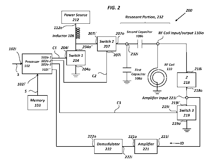
material, large equipment/antenna sizes that are incompatible with easy
installation/removal of
1
CA 03164327 2022-06-10
WO 2021/119299 PCT/US2020/064292
buried sensors, and excessive power consumption incompatible with long-term or
battery-
powered operation.
[0005] In general, improved systems and methods are provided for two way
communication by
sub-surface sensors.
[0006] In an embodiment, a transceiver circuit is provided and includes a
resonant portion, a
plurality of switches, a first complex impedance, an amplifier, and a
demodulator. The resonant
portion can include a single radiofrequency (RF) coil and the resonant portion
can be configured
for transmission and reception at about the same frequency. The plurality of
switches can
include a first switch, a second switch, and a third switch. The first switch
can include an input
in electrical communication a power source and an output in electrical
communication with
ground. The second switch can include an input interposed between the power
source and the
first switch and an output in electrical communication with an input of the
resonant portion. The
third switch can include an input in electrical communication with an output
of the resonant
portion and an output in electrical communication with ground. The first
complex impedance
can be interposed between the output of the resonant portion and the input of
the third switch.
The amplifier can include an amplifier input interposed between the first
impedance and the
input the third switch. The demodulator can include an input in electrical
communication with
the amplifier output.
[0007] In an embodiment, the circuit can also include a processor and a sensor
in electrical
communication with the processor. The processor can be configured to receive
one or more
sensor measurement signals output by the sensor. The one or more measurement
signals can
include data characterizing at least one parameter of a subsurface material
measured by the
sensor.
[0008] In another embodiment, the processor is configured to command the
second and third
switches to close and command the first switch to open and close at a closure
frequency that
provides current from the power source to the radiofrequency coil in the form
of a carrier signal.
The carrier signal can be transmitted by the radiofrequency coil at a
transmission frequency. The
2
CA 03164327 2022-06-10
WO 2021/119299 PCT/US2020/064292
amplifier and the demodulator can be electrically isolated from the resonant
portion when the
second and third switches are closed.
[0009] In another embodiment, the carrier signal can be a square wave
representing at least a
portion of the sensor measurement signal.
[0010] In another embodiment, a capacitance of the resonant portion, an
inductance of the
resonant portion, and the closure frequency can be selected such that the
carrier frequency is a
sinusoid.
[0011] In another embodiment, the first impedance can be a variable impedance
configured to
shift a resonant frequency of an oscillator formed by resonant portion and the
first impedance to
be approximately equal to the transmission frequency.
[0012] In another embodiment, the processor can be configured to command the
second and
third switches to open such that an oscillating signal received by the
radiofrequency coil is
received at the input of the amplifier. The amplifier can also be configured
to amplify the
received oscillating signal. The demodulator can be configured to receive the
amplified
oscillating signal, demodulate the amplified oscillating signal; and output a
data signal generated
from the demodulated amplified oscillating signal to the processor. The
resonant portion can
also be isolated from the power source when the second and third switches are
open.
[0013] In another embodiment, at least one of the second and third switches is
a diode.
[0014] In another embodiment, the resonant portion can also include a first
capacitor and a
second capacitor.
[0015] In another embodiment, an input of the first capacitor can be in
electrical communication
with the output of the second switch and an output of the first capacitor is
in electrical
communication with ground. An input of the second capacitor can also be in
electrical
communication with the output of the second switch and an output of the second
capacitor is in
electrical communication with the radiofrequency coil.
3
CA 03164327 2022-06-10
WO 2021/119299 PCT/US2020/064292
[0016] In another embodiment, resonant portion also further includes a second
complex
impedance, a fourth switch, and a fifth switch. The second complex impedance
can include an
input in electrical communication with the input of the resonant portion. The
fourth switch can
include a first input, a second input and an output. The first input can be
electrical
communication with the processor. The second output can be in electrical
communication with
an output of the second complex impedance. The output can be in electrical
communication with
ground. The fifth switch can include a first input, a second input, a third
complex impedance,
and an output. The first input can be in electrical communication with the
processor. The
second input can be in electrical communication with the input of the resonant
portion. The
output can be in electrical communication with an input of a third complex
impedance. The third
complex impedance can include an output in electrical communication with an
input/output of
the RF coil. The processor can be further configured to command the second and
third switches
to open and close to shift a resonant frequency of an oscillator formed by
resonant portion.
[0017] In another embodiment, the data signal can be operative to cause the
processor to
command the sensor to cease output of the sensor measurement signal.
[0018] In another embodiment, the data signal can be operative to cause the
processor to
command the sensor change an interval between respective transmissions of the
sensor
measurement signal.
[0019] In another embodiment, the data signal can be operative to cause the
processor to change
a power of the carrier signal.
[0020] In another embodiment, the data signal can be operative to cause the
processor to
command the circuit to transmit the sensor measurement signal upon receipt of
the data signal.
DESCRIPTION OF DRAWINGS
[0021] These and other features will be more readily understood from the
following detailed
description taken in conjunction with the accompanying drawings, in which:
[0022] FIG. 1 is a diagram illustrating one exemplary embodiment of a one-way
(transmit only)
communication circuit;
4
CA 03164327 2022-06-10
WO 2021/119299 PCT/US2020/064292
[0023] FIG. 2 is a diagram illustrating one exemplary embodiment of a two-way
(transmit and
receive) communication system;
[0024] FIG. 3 is a diagram illustrating an effective transmission circuit
provided by the two-way
communication system of FIG. 2 in a transmission configuration;
[0025] FIG. 4 is a diagram illustrating an effective reception circuit
provided by the two-way
communication system of FIG. 2 in a reception configuration;
[0026] FIG. 5 is a diagram illustrating an alternative embodiment of the two-
way
communication system of FIG. 2;
[0027] FIG. 6 is a diagram illustrating another alternative embodiment of the
two-way
communication system of FIG. 2;
[0028] FIG. 7 is a diagram illustrating an operating environment including an
above ground
transmit and receive (AGTR) unit and a below ground transmit and receive
(BGTR) unit; and
[0029] FIGS. 8A-8B are diagrams illustrating operating environments employing
coil rotation for
determining location in a beacon mode of operation. (A) Maximum received
signal geometry. (B)
Minimum (null) received signal geometry.
[0030] It is noted that the drawings are not necessarily to scale. The
drawings are intended to
depict only typical aspects of the subject matter disclosed herein, and
therefore should not be
considered as limiting the scope of the disclosure.
DETAILED DESCRIPTION
[0031] In agriculture, sensing systems have been developed to communicate
measurements of
soil conditions (e.g., temperature, moisture, salinity, etc.) from below-
ground sensors to above-
ground receivers. As an example, a measurement system including a sensor and a
wireless
transmitter are installed below ground. Measurement data acquired by the
sensor are received by
the transmitter and in turn, wirelessly transmitted to an above ground
receiver. Once received by
CA 03164327 2022-06-10
WO 2021/119299 PCT/US2020/064292
the above ground receiver, the measurement data can be stored locally and/or
forwarded to a
network.
[0032] However, existing systems of this type are limited. As an example, the
below ground
unit is configured for transmission only, also referred to as a below ground
transmit only
(BGTO) unit. The above ground unit is configured for reception only, also
referred to as a above
ground reception only (AGRO) unit. As a result, the transmission behavior of
the BGTO is fixed
at the time of installation via firmware. Thus, the BGTO essentially operates
autonomously and
independently of the AGRO, and can only be altered via instructions triggered
by the sensor
measurements (e.g., curtailing a measurement interval when soil is cold and
plant growth has
ceased).
[0033] As discussed in detail below, an improved two-way communication system
is described
that provides transmission and reception capability. In one embodiment, the
two-way
communication system can be employed in the below ground unit, referred to as
below ground
transmit and receive (BGTR) unit. In another embodiment, the two-way
communication system
can also be employed in the above ground transmit and receive (AGTR),
respectively. The
ability of the BGTR to receive updated instructions operative to modify
transmission behavior of
the BGTR after initial deployment can provide a variety of added
functionality, including on-
demand transmission and bug fixes, as well as improved battery life.
[0034] Embodiments of the disclosed two-way communication systems and
corresponding
methods are discussed herein in the context of measurement of soil conditions
for agricultural
applications. However, embodiments of the disclosure can be employed with any
sensor in any
sub-surface environment and/or application without limit. Examples of other
applications for the
disclosed embodiments can include, but are not limited to, pipelines (e.g.,
oil and gas), buried
tank leak detection/monitoring, structural integrity monitoring (e.g., dams,
canals, levies, etc.),
monitoring concrete curing, monitoring ballast materials under road beds,
traffic monitoring.
[0035] In order to better understand the improvements and corresponding
benefits provided by
embodiments of the disclosed two-way communication system, a block diagram
illustrating a
circuit of an existing one-way below ground transmission only (BGTO) unit 100
is discussed
6
CA 03164327 2022-06-10
WO 2021/119299 PCT/US2020/064292
with respect to FIG. 1. As shown, the BGTO unit 100 includes a processor 102
(e.g., a
microcontroller), a memory 103, a switch 1004, a resonant portion 109, and a
power source 112.
[0036] The processor 102 can be configured to receive a measurement signal S
at an input. The
measurement signal can be received directly from a sensor (not shown) via a
first input 102i,
received from the memory via second input 102i', or combinations thereof. An
output 102o of
the processor 102 can be connected to an input 104i of the switch 104.
[0037] The switch 104 further includes a first output 104o and a second output
104o'. The first
output 104o is connected to ground. The second output 104o' is connected to an
input 109i of
the resonant portion 109. The input 109i is further in communication with the
inductor 106.
The first output 104o of the switch 104 is connected to ground. The switch 104
is configured to
move between an open position and a closed position in response to commands
from the
processor 102. As an example, the processor can provide command signals C to
the switch 104
at the input 104i. In certain embodiments, the switch 104 can be a transistor.
[0038] In an embodiment, the power source 112 can be a battery or other source
of DC power.
As an example, the power source 112 can be configured to provide voltage
within the range from
about 1.5 V to about 15 V and current from about 10 mA to about 500 mA,
depending on the
desired transmit power level. The inductor 106 is interposed between the
output 112o of the
power source 112 and the junction 105.
[0039] The resonant portion 109 includes a first capacitor 108a, a second
capacitor 108b, and a
radiofrequency (RF) coil 110. The first capacitor 108a is connected at one end
to the input 109i
of the resonant portion 109 and at the other end to ground. The second
capacitor 108b is
connected at one end to the input 109i of the resonant portion 109 and at the
other end to an input
110i of the RF coil 110.
[0040] When the switch 104 is closed, current flows from the power source 112,
through the
inductor 106, through the switch 104 to ground. When the switch 104 is open
the energy in the
inductor 106 couples into the first and second capacitors 108a, 108b, and the
RF coil 110, which
behaves electrically as an inductor.
7
CA 03164327 2022-06-10
WO 2021/119299 PCT/US2020/064292
[0041] The command signal C can be a square wave which produces a simple on-
off cycle in the
switch 104. A switch closure frequency f0, the capacitance of the first and
second capacitors
108a, 108b, and the inductance of the RF coil 110 can be selected such that a
sinusoidal voltage
signal is applied to the RF coil 110 with high energy efficiency. The
oscillating voltage across
the RF coil 110 gives rise to an oscillating current, also referred to herein
as a carrier signal fc.
The carrier signal fc produces an oscillating magnetic field, referred to
herein as a transmission
signal T, which can be received by a receiver (e.g., an AGRO unit, not shown).
By suitable
variation in the command signal C and the carrier signal fc, the transmission
signal T, can be
modulated to carry data, such as measurement data received by the processor
102 from a sensor.
[0042] One feature of this approach is that, for convenient sizes of the RF
coil 110 and
communication ranges, the coil size is typically over 3 inches in diameter and
requires hundreds
of volts across the RF coil 110 to generate an carrier signal with sufficient
amplitude to produce
a transmission signal T that can be received by the AGRO unit. The voltage at
the input 109i of
the resonant portion 109 is also generally fairly high (often well in excess
of 20V).
[0043] As noted above, it can be desirable to add reception capability to the
BGTO unit 100 of
FIG. 1. In one approach, this can be accomplished by adding a second circuit
including a second
RF coil to provide the reception capability. However, this configuration is
not desirable for a
number of reasons. First, the two coils can couple and affect each other
strongly when close
(e.g., at separation distances less than a couple of coil diameters),
influencing transmission and
reception by the respective RF coils. While this coupling can be addressed by
separating the
respective RF coils at a larger distance, this added separation increases the
size of the resulting
transmit/receive unit. Second, the additional RF coil and circuitry can
significantly increase the
cost and complexity of production and assembly.
[0044] In another approach, receive capability can also be added to the BTGO
unit 100 of FIG. 1
by adding an amplifier within a tuned LC "tank circuit" formed by the resonant
portion 109. For
effective signal transmission, the resonant portion 109 must satisfy the
following equations:
1
fl= ____________________________________________ Eq. 1
27rA/C108b * L110
8
CA 03164327 2022-06-10
WO 2021/119299 PCT/US2020/064292
1
f2= Eq. 2
2ff-as * L110
1 1 1
Cs = Eq. 3
C108a C108b
f1< f , f2 > f Eq.4
where C108a is the capacitance of the first capacitor 108a, C108b is the
capacitance of the
second capacitor 108b, Cs is the effective capacitance of the first and second
capacitors 108a,
108b in series, L110 is the inductance of the RF coil 110, f is the desired
transmission frequency
fl and f2 are frequencies. In general, the closer fl and f2 approach f, the
greater the transmit
signal T, limited by the non-ideal properties of the components. When these
relations are
satisfied, it is possible to efficiently convert energy from the power source
112 to transmission
signal T in the form of a high voltage across the RF coil 110.
[0045] To receive an incoming signal from the above ground unit, it is
desirable that the
structure formed by the inductor 106 and the resonant portion 109 is resonant
at the transmission
frequency f This would allow an amplifier and demodulator to be used at either
the input 109i
of the resonant portion 109, or preferably, the input 110i to the RF coil 110,
to receive the
incoming signal. By making this resonant at the transmission frequency f, the
required amplifier
gain can be reduced and the resultant system can strongly reject signals that
are not at the
transmission frequency due to the narrow bandwidth. That is, a "tank" circuit
is created at the
desired reception frequency.
[0046] Two significant challenges arise when attempting to achieve this goal.
In one aspect, it is
not practically possible to simultaneously satisfy the transmission equations
1-4 while also
creating a resonant structure for receiving at the transmission frequency. In
another aspect,
during transmission, the voltage in the circuit can be hundreds of volts AC.
It is very difficult to
integrate an amplifier into this circuit that can amplify very small
(potentially sub-millivolt
signals), while tolerating the hundreds of volts during transmission and not
affecting the
carefully tuned elements needed for transmission and reception.
9
CA 03164327 2022-06-10
WO 2021/119299 PCT/US2020/064292
[0047] Embodiments of the present disclosure provide solutions to these
challenges by
modifying the circuit of the BGTO unit 100 of FIG. 1 to include additional
reactive elements and
switches (FIG. 2) to provide a two-way transmit and receive unit 200, also
referred to herein as
transceiver system 200. As discussed in greater detail below, the transceiver
system 200 can be
employed as a below ground transmit and receive (BGTR) unit, an above ground
transmit and
receive (AGTR) unit, and combinations thereof.
[0048] As shown, the transceiver system 200 is modified with respect to the
BGTO unit 100 to
include a first switch 204, a second switch 207, a third switch 219, resonant
portion 232, an
amplifier 221, and a demodulator 222. The resonant portion 232 differs from
the resonant
portion 109 by the addition of a complex impedance 218, which can become part
of the resonant
portion 232 when the switch 219 is closed. Components in common between the
transceiver
system 200 and the BGTO unit 100 (e.g., processor 102, memory 103, inductor
106, power
source 112) are provided as discussed above, unless otherwise noted.
[0049] The first switch 204 includes an input 204i, a first output 204o and a
second output 204o'.
The input 204i is connected to a first output 102o-1 of the processor 102. The
first output 104o
is connected to ground. The second input 204i' is connected to the inductor
106. The first
switch 204 is configured to move between an open position and a closed
position in response to
first command signals Cl received from the processor 102 via the input 204i.
In certain
embodiments, the first switch 204 can be a transistor.
[0050] The second switch 207 includes a first input 207i, a second input
207i', and an output
207o. The first input 207i is connected to a second output 102o-2 of the
processor 102. The
second input 207i' is interposed between the inductor 106 and the second
output 204o' of the first
switch 204. The output 207o of the second switch 207 is connected to the input
109i of the
resonant portion 232. The second switch 207 is configured to move between an
open position
and a closed position, with respect to the first input 207i and the output
207o of the complex
impedance 219, in response to second commands signals C2 received from the
processor 102 via
the first input 207i. In certain embodiments, the second switch 207 can be a
transistor.
CA 03164327 2022-06-10
WO 2021/119299 PCT/US2020/064292
[0051] The complex impedance 218 includes an input 218i and an output 2180.
The input 218i
is connected to the RF coil 110 (e.g., an RF coil input/output 110io), and the
output 218o is
connected to an input 219i' of the third switch 219. While the complex
impedance 218 is
generalized in FIG. 2 as a single component, it can be understood that the
complex impedance
218 can include one or more components, such as resistors, capacitors,
inductors, or any
combination thereof The components can have fixed or adjustable electrical
parameters (e.g.,
capacitance, inductance, impedance). Examples of adjustable components of the
complex
impedance can include a tunable capacitors or dip switches with multiple fixed
capacitors that
allow for a changing effective impedance.
[0052] The third switch 219 includes a first input 219i, a second input 219i',
and an output 219o.
The first input 219i is connected to a third output 102o-3 of the processor
102. The second input
219i' is connected to output 218o of the complex impedance 218. The output
2190 of the third
switch 219 is connected to ground. The third switch 219 is configured to move
between an open
position and a closed position (with respect to the input 219' and the output
2190 of the complex
impedance 219) in response to third commands signals C3 received from the
processor 102 via
the first input 219i. In certain embodiments, the third switch 219 can be a
transistor.
[0053] The amplifier 221 can include an input 221i and an output 221o. The
input 221i is in
communication with the output 218o of the complex impedance 218 (e.g.,
interposed between
the output 218o of the complex impedance 218 and the second input 219i' of the
third switch
219). The output 2210 of the amplifier 221 is in communication with an input
222i of the
demodulator 222. An output 222o of the demodulator 222 is in communication
with a third
input 102i" of the processor 102. The amplifier 221 and the demodulator 222
can be employed
to receive instruction data ID from the resonant portion 232 when the
transceiver system 200
operates in a reception mode, demodulate the instruction data ID, and provide
the instruction
data ID to the processor 102.
[0054] To operate in a transmission configuration, the processor 102 commands
the second
switch 207 and the third switch 219 to close via command signals C2 and C3. A
diagram of an
effective transmission circuit 300 resulting from closure of the second and
third switches is
illustrated in FIG. 3. To operate in a reception configuration, the processor
102 commands the
11
CA 03164327 2022-06-10
WO 2021/119299 PCT/US2020/064292
second switch 207 and the third switch 219 to open via command signals C2 and
C3. A diagram
of an effective reception circuit 400 resulting from opening the second and
third switches is
illustrated in FIG. 4.
[0055] Closure of the second switch 207 in the transmission configuration
allows electrical
communication between the power source 212, the inductor 106, and the resonant
portion 232.
Closure of the third switch C3 holds the amplifier input 221i at ground. This
protects the
amplifier 221 from input of high voltage from the RF coil 110 during
transmission, as discussed
below. Isolation of the amplifier 221, in turn, substantially reduces or
negates effect of the
amplifier 221 on the tuning needing for effective transmission. The amplifier
221 and
demodulator 222 are not shown in FIG. 3, as they have substantially no effect
on operation in the
transmission configuration. Thus, the effective transmission circuit 300 of
FIG. 3 is analogous to
the transmission circuitry of the BGTO unit 100 of FIG. 1, with addition of
the complex
impedance 218 in parallel with the RF coil 110.
[0056] The transmission signal T can be generated by the transceiver system
200 in a similar
manner to that discussed with respect to FIG. 1 when the second and third
switches 207, 219 are
closed. The processor 102 commands the first switch 204 to turn on and off to
transmit. When
the first switch 204 is closed (e.g., in response to first command signals Cl
from the processor
102), current flows from the power source 112, through the inductor 106, to
the input 232i of the
resonant portion. The energy in the inductor 106 couples into the first and
second capacitors
108a, 108b, and the RF coil 110, which behaves electrically as an inductor.
When the first
switch 204 is open, input 232i of the resonant portion 232 is coupled to
energy stored in the
inductor 106, causing the resonant portion 232 to oscillate.
[0057] The first command signal Cl can be a square wave which produces a
simple on-off cycle
in the first switch 204. The switch closure frequency f., the capacitance of
the first and second
capacitors 108a, 108b, the inductance of the RF coil 110, and the impedance
218 (which is part
of the resonant portion 232 when the switch 219 is closed in the transmit
configuration) can be
selected such that a sinusoidal voltage signal is applied to the RF coil 110
with high energy
efficiency. The oscillating voltage across the RF coil 110 gives rise to an
oscillating current, the
carrier signal fc. The carrier signal fc, produces an oscillating magnetic
field, the transmission
12
CA 03164327 2022-06-10
WO 2021/119299 PCT/US2020/064292
signal T, that can be received by a receiver (e.g., an AGRO unit, not shown).
By suitable
variation in the command signal C, and the carrier signal fc, the resultant
transmission signal T
can be modulated to carry data, such as measurement data received by the
processor 102 from
the sensor.
[0058] In this transmission configuration, using appropriate values for the
components of the
resonant portion 232 (e.g., capacitance of the first capacitor 108a and the
second capacitor 108b,
the inductance of the RF coil 110, and the impedance of the variable impedance
218), it is
possible to achieve the required conditions for effective high transmit
voltage of the RF coil 110.
The capacitance of the first capacitor 108a can be selected from about 100pF
to about 10,000 pF.
The capacitance of the second capacitor 108b can be selected from about 100pF
to about
10,000pF. The inductance of the RF coil 110 can be selected from about 0.1mH
to about 10mH.
The impedance of the complex impedance 218 can be selected from about +10,000i
ohms to
about -10,000i ohms.
[0059] Opening the third switch 219 permits electrical communication between
the RF coil
input/output 110io and the input 221i of the amplifier 221, through 218. This
reception
configuration exposes the amplifier 221 to any received oscillating signals
formed by the
resonant portion 232 (which is formed from the first capacitor 108a, the
second capacitor 108b,
and the RF coil 110 as the second switch 207 and the third switch 219 are open
and the input
impedance of the input 221i of the amplifier 221 is relatively high), such as
instruction data ID.
Opening the second switch 207 in the reception configuration further inhibits
electrical
communication between the power source 212 and inductor 106 with the resonant
portion 232.
Accordingly, the power source 212 and inductor 106, along with the first
switch 204 and the
second switch 207, are not shown in FIG. 4, because they have no effect on
reception. As
discussed below, it is possible to simultaneously achieve the appropriate
tuning required for
transmission and also an appropriately tuned tank circuit for reception.
[0060] The conditions for effective transfer of a high voltage to the
transmitting current in the
transmission configuration is similar to the earlier conditions illustrated in
Equations 1¨ 4:
13
CA 03164327 2022-06-10
WO 2021/119299 PCT/US2020/064292
1
fl= ______________________________________________ Eq. 5
27rVC108b * Lp
1
f2= ______________________________________________ Eq. 6
2ff-as * L110
1 1 1
Cs = Eq. 7
C108b C108a
1 1 1
Lp
¨ = ¨ L110 + ¨ L218 Eq. 8
f1 f , f2 > f Eq. 9
where L218 is the inductance of the complex impedance 218 and Lp is an
inductance that can be
used to simultaneously achieve optimum transmit and receive characteristics in
one overall
circuit employing a single RF coil for both signal transmission and reception.
In certain
embodiments, Lp can be selected from the range of about 1 mH to about 10 mH.
[0061] With regards to the effective reception circuit 400, the impedance of
the amplifier 221 in
the reception configuration can be made quite high compared to the other
circuit elements and
can be ignored. For effective reception, the resonant portion 232 needs to be
resonant at the
reception frequency, f This condition is expressed as:
1
f = Eq.10
2ff-as * L110
1 1 1
Cs = Eq. 11
C108a C108b
As there are three degrees of freedom, C108a, C108b, and L218, it is possible
to simultaneously
satisfy Equations 9 and 10 and achieve optimum reception combined with
efficient transmission.
[0062] In an alternative embodiment, the resonant portion 232 of the
transceiver system 200 can
be provided in the form of transceiver system 500 to facilitate shifting the
resonant frequency.
As shown in FIG. 5, the transceiver system 500 is modified from the
transceiver system 200 by
adding a second complex impedance 218b, a third complex impedance 218c, a
fourth switch
14
CA 03164327 2022-06-10
WO 2021/119299 PCT/US2020/064292
502, and a fifth switch 504. For clarity, the complex impedance 218 is
renumbered as first
complex impedance 218a. Similar to the first complex impedance 218a, while the
second and
third complex impedance 218b, 218c are generalized as a single component in
FIG. 5, it can be
understood that the second and third complex impedance 218b, 218c can include
one or more
components, such as resistors, capacitors, inductors, or any combination
thereof The
components can have fixed or adjustable electrical parameters (e.g.,
capacitance, inductance,
impedance).
[0063] The second complex impedance 218b includes an input 218bi and an output
218bo. The
input 218bi is connected to an input 532i of the resonant portion 532 and the
output 218bo is
connected to a second input 502i' of the fourth switch 502. The impedance of
the second
complex impedance 218b can be selected from about 10,000i ohms to about -
10,000i ohms.
[0064] The fourth switch 502 includes a first input 502i, the second input
502i', and an output
502o. The first input 502i is connected to a fourth output 102o-4 of the
processor 102, and the
second input 502i' is connected to the output 218bo of the second complex
impedance 218b. The
output 502o is connected to ground. The fourth switch 502 is configured to
move between an
open position and a closed position in response to fourth commands signals C4
received from the
processor 102 via the first input 502i. In certain embodiments, the fourth
switch 502 can be a
transistor.
[0065] The fifth switch 504 includes a first input 504i, the second input
504i', and an output
504o. The first input 504i is connected to a fifth output 102o-5 of the
processor 102, and the
second input 502i' is connected to the input 532i of the resonant portion 532
(e.g., interposed
between the input 532i of the resonant portion 532 and the input 218bi of the
second complex
impedance 218b). The output 504o of the fifth switch 504 is connected to an
input 218ci of the
third complex impedance 218c. The fifth switch 504 is configured to move
between an open
position and a closed position in response to fifth commands signals C5
received from the
processor 102 via the first input 504i. In certain embodiments, the fifth
switch 504 can be a
transistor.
CA 03164327 2022-06-10
WO 2021/119299 PCT/US2020/064292
[0066] The third complex impedance 218c includes an input 218ci and an output
218co. The
output 218co is connected to the RF coil input/output 110io. The impedance of
the third
complex impedance 218c can be selected from about 10,000i Ohms to about -
10,000i Ohms.
[0067] The third complex impedance 218c, under control of the fifth switch 504
can be used to
modify the effective impedance of the second capacitor 108b (when the fifth
switch is closed) by
adding in parallel the third complex impedance when the fifth switch 204 is
closed or by
removing the third complex impedance 218c when the fifth switch 504 is open.
Likewise, the
second complex impedance 218b can be used to modify the effective impedance of
the first
capacitor 108a. With these additions, it is also possible to satisfy the
constraints for effective
transmission and reception by suitable combinations of switch positions.
[0068] Embodiments of the transceiver systems 200, 500 can be further modified
to replace at
least one of the second switch 207 and the third switch 219 with diodes. FIG.
6 illustrates a
transceiver system 600 which modifies the transceiver system 200 to replace
the second switch
207 and the third switch 219 with diodes. As shown, diodes 507a, 507b replace
the second
switch 207 and diodes 519a, 519b replace the third switch 219.
[0069] This modification can simplify the transceiver system 600 as compared
to the transceiver
system 200. In general, diodes exhibit little current flow when subject to a
forward voltage
below their intrinsic forward voltage drop (typically from about 0.1 to 1V)
and very high current
flow at voltages above this. During transmission, when the first switch 204 is
opened and closed
(turned on and off), the voltage across the diodes 607a, 607b is relatively
high (e.g., about 10 V
or greater), such that the diodes 607a, 607b mimic the closed second switch
207. Similarly, the
diodes 519a, 519b act like a closed switch (e.g., the third switch 219) and
limit the voltage into
the amplifier 221 to a volt or less, substantially preventing any adverse
issues with the amplifier
221.
[0070] When the transmission is off (the first switch 204 in the open
position), the RF coil 110 is
exposed to the oscillating magnetic field of a transmitter, which induces a
small voltage in the
circuit (e.g., on the order of about 1 mV to about 100 mV). Under these low
voltages, the diodes
607a and 607b, as well as 619a and 619b, act like closed switches (e.g., the
second switch 207
16
CA 03164327 2022-06-10
WO 2021/119299 PCT/US2020/064292
and the third switch 219, respectively), as they present a very high impedance
to a low voltage.
Furthermore, the amplifier 221 sees the full received AC signal at the input
221i because the
impedance of the amplifier 221 is very high compared to the impedance of the
complex
impedance 218. As a result, the voltage at the input 221i of the amplifier 221
is approximately
the same as that at the RF coil input/output 110io.
[0071] An embodiment of the transceiver system 600 has been implemented in
hardware and
signals of over 200V AC were generated across the RF coil 110 when in the
transmitting
configuration. In the reception configuration, the transceiver system 600 is
capable of receiving
and demodulating an oscillating signal from a transmitter over 7m distant.
Beneficially, this
demonstrates that very low cost diodes 607a, 607b, 619a, 619b can successfully
replace the
second and/or third switches 209, 219. Furthermore, no control of switches by
the processor 102
is needed.
[0072] FIG. 7 is a block diagram illustrating an operating environment 700
employing
embodiments of the transceiver system discussed above. As shown, an above
ground transmit
and receive (AGTR) unit 702 is positioned above a surface 704 of a material
708 (e.g., soil,
concrete, water, etc.) and is in communication with a network 706. A below
ground transmit and
receive (BGTR) unit 710 is positioned below the surface 704 and is in
communication with one
or more sensors (collectively represented as sensor 712). Embodiments of the
AGTR unit 702
and the BGTR unit 710 can include an embodiment of the transceiver system 200,
500, or 600.
[0073] The one or more sensors 712 are in communication with the BGTR unit 710
and can be
configured to measure one or more parameters of the material 708. As an
example, when the
material 708 is soil, the sensor(s) 712 can be configured to measure soil
parameters such as
moisture, salinity, and/or temperature. When the material 708 is a different
media (e.g.,
concrete, water, etc.), other parameters can be measured by the sensor(s) 712.
Examples of such
parameters can include, but are not limited to, light level, fluid flow rate,
vibration amplitude,
and the like.
[0074] In use, the BGTR unit 710 can execute instructions operative to control
acquisition of
respective measurement data by the sensor 712, to control wireless
transmission of measurement
17
CA 03164327 2022-06-10
WO 2021/119299 PCT/US2020/064292
data received from the sensor 712 to the AGTR unit 702 (measurement signals
716s), and
combinations thereof. As discussed above, without reception capability, the
below ground unit
can be limited to executing instructions received prior to deployment below
ground. However, a
variety of added functionality can be implemented when the below ground unit
includes the
ability to receive updated instructions.
[0075] Updated instructions received by the BGTR unit 710 can be operative to
perform one or
more of the following:
= Increasing a first time interval between respective measurements acquired
by the
sensor 712, alone or in combination with increasing a second time interval
between
transmission of respective sensor measurement signals 716s by the BGTR unit
710.
It can be beneficial to increase the first and/or second time intervals during
irrigation
in order to better capture important soil properties (e.g., water infiltration
rates).
= Decreasing the first time interval between respective measurements
acquired by the
sensor 712, alone or in combination with decreasing the second time interval
between
transmission of respective sensor measurement signals 716s by the BGTR unit
710.
It can be beneficial to decrease the first and/or second time intervals when
the rate of
change of measured parameters is anticipated to be relatively low (e.g., after
a crop
has been harvested, during the fallow season, etc.) in order to conserve the
lifetime of
the power source 112 (e.g., a battery).
= Updating firmware of the BGTR unit 710 to allow for bug fixes in software
and/or
instructions executed by the BGTR unit 710. In general, existing BGTO units
(e.g.,
100) are sealed to prevent water intrusion. Thus, even if a BGTO unit 100 were
removed from below ground, there is no practical mechanism for updating its
firmware.
[0076] The ability of the BGTR unit 710 to receive control signals 714s can
further enable the
following functionality:
= The BGTR unit 710 can periodically receive a control signal 714s from the
AGTR
unit 702 providing a notification that the AGTR unit 702 is present. (e.g., an
"I'm
18
CA 03164327 2022-06-10
WO 2021/119299 PCT/US2020/064292
here!" message). If the AGTR unit 702 is removed from the field, the BGTR unit
710
can instruct the sensor 712 to cease measurement and further cease
transmission of
sensor measurement signals 716s to increase battery life.
= The AGTR unit 702 can measure the strength of the sensor measurement
signals 716s
transmitted by the BGTR unit 710. If the strength is sufficiently high, the
AGTR unit
702 can transmit a control signal 714 instructing the BGTR unit 710 to reduce
the
transmit power and hence increase battery life of the BGTR unit 710.
= The BGTR unit 710 can periodically receive a control signal 714s from the
AGTR
unit 702 instructing the BGTR unit 702 to transmit a sensor measurement signal
716s
upon receipt. In this manner, "on demand" soil data acquisition can be
accomplished.
[0077] The ability of the AGTR unit 702 to command the BGTR unit 710 to make
an on demand
measurement and transmit the result can facilitate applications where the AGTR
unit 702 is not
fixed in the field close to a single (or multiple) BGTR units 710. As an
example, an AGTR unit
702 can be placed on a piece of farm equipment such as a tractor, on a center
pivot boom arm, or
on a ground or aerial drone. This opens up the ability of a mobile AGTR unit
(MAGTR unit
702s) to cover a large number of fixed BGTR units 710, and hence a large
physical footprint.
[0078] Without the ability of two-way capability on the BGTR unit 710 and the
MAGTR
unit 702m, the mobile above ground unit would be required to linger over the
below ground unit
until a regularly scheduled measurement and transmission occurs. For context,
in order to
conserve battery life, the measurement/transmission interval is typically in
the range of about 10-
60 minutes. In existing systems, this can force the above ground unit to
remain in the vicinity of
the below ground unit for up to one hour, making data acquisition difficult
and time consuming.
With two-way communication the MAGTR unit 702m can arrive at the vicinity of
the BGTR
unit 710, send a message to the BGTR unit 710 to initiate a
measurement/transmission cycle,
receive the measurement data, and then start on the way to another BGTR unit
710 with roughly
seconds of dwell time at each location. The MAGTR unit 702m can then send the
received
measurement data to the network 706 using a conventional radio immediately or
wait until it
returns to a home location where other options are available for upload to the
network 706.
19
CA 03164327 2022-06-10
WO 2021/119299 PCT/US2020/064292
Beacon Mode
[0079] Besides transmitting data, embodiments of the transceiver systems
discussed herein (e.g.,
200, 500, 600, 700) can be employed to convey location information for use in
recovering a
BGTO or BGTR, place an above-ground AGRO or AGTR close enough to the below
ground
unit for reliable reception, and as an aide in mobile above ground receiver
(MAGTR)
applications.
[0080] With further reference to the transceiver system 200 of FIG. 2, a
beacon signal can be
generated by controlling the first switch 204. In order to provide a concrete
example of an
implemented system, during data transmission, the first switch 204 is turned
on/off at a
predetermined switch closure frequency to generate a sinusoidal signal having
a high amplitude
across the RF coil 110. As an example, a switch closure frequency of about
174kHz can
generate a sinusoidal 174kHz signal of 100's of volts across the RF coil 110.
Using an on-off
keying, a "1" is sent by closing the first switch 204 for a predetermined time
(e.g., about lms)
and "0" is sent by opening the first switch 204 for a predetermined time
(e.g., about lms).
During data reception, the receiver formed by the amplifier 221 and the
demodulator 222
converts a received weak voltage received across the RF coil 110 into a logic
input to the
processor 102.
[0081] The reception distance can be in the range of about 5m to about 20m for
a typical
transmitted signal. Furthermore, the interval between sensor measurements and
transmissions
can be long (e.g., an hour or more). Thus, using regular data transmission for
location is highly
problematic. In one aspect, an interval of one hour between transmissions
makes locating a
below ground unit impractical, many hours can be required to locate the below
ground unit, even
with a rough GPS location. In another aspect, the extended range is
problematic. At best, a
relative location within about 5m is provided, rather than a precise location.
This is insufficient
for recovering the below ground unit or to establish that an above ground
receiver is within
reliable communication range across varying environmental factors.
[0082] These two limitations can be overcome by using a beacon mode that sends
one or more
signals of varying power levels at frequent interval. The lower power levels
can allow much
CA 03164327 2022-06-10
WO 2021/119299 PCT/US2020/064292
more precise location (e.g., down to as low as about 10cm or better) and more
frequent signals
allows for a quick determination of location once the general area of the
below ground unit is
established. The use of frequent signals can require very efficient battery
utilization in order to
allow the power source 212 (e.g., a battery) of the below ground unit to
support operation for 5
years or more. Simple beacon routines that can operate autonomously of the
processor 102 are
also desirable to conserve battery power and offer additional flexibility.
[0083] Two approaches have developed for the locating pulse(s). The first
approach employs a
short train of 174kHz on/off control of the first switch 204, which can be
much shorter than the
current lmS train time when sending data. In another aspect, a single closure
of the first switch
204 having variable duration, referred to herein as hammering. In both cases,
the resonant
structure in the resonant portion 232 does not turn on immediately at maximum
strength at the
start of the switch closure train, but rather ramps up. An analogy for this
first approach is that of
pushing a swing with a series of pushes, where the amplitude of the swing
slowly builds up with
each push. Continuing this analogy, the swing need to be pushed at the right
time (e.g., the right
frequency), otherwise the amplitude doesn't build up much.
[0084] In the second approach using a single pulse (hammering), the energy
from the pulse starts
the transmitter oscillating at the natural frequency (e.g., 174kHz) for a
period of time as it decays
from losses in the circuit. Additionally, the longer the pulse, the more
energy is imparted and the
stronger the oscillation. An analogy for this second approach is striking a
bell with a hammer,
causing it to ring at its natural frequency. A harder hit (in the case of a
circuit, a longer pulse)
generates a louder sound, but does not change the tone.
[0085] In both beacon approaches, the amplitude of the oscillation on the RF
coil 110, and hence
the transmit strength, can be made much smaller and the duration can be much
shorter. These
combine to produce an energy requirement for the beacon that is much smaller
than typically
used to send data, helping to converse battery life. The lower transmit
intensity can reduce the
reception range, which can provide more accurate localization of the below
ground unit. For
example, if the beacon pulse range is lm, the beacon can only be detected
within lm of it. In
contrast, with a typical transmission strength having a range of 5-20m, the
smallest localization
that can be determined is within 5-20m.
21
CA 03164327 2022-06-10
WO 2021/119299 PCT/US2020/064292
[0086] In alternative embodiments, it can be possible to increase the
transmission strength by
increasing the input voltage at the input 232i to the resonant portion 232.
Conversely, the
transmission strength can be decreased by decreasing the input voltage at the
input 232i to the
resonant portion 232).
[0087] It can be understood that, while 174kHz has been discussed in examples
above as the
operating frequency, other values can be employed.
[0088] As an example of how power efficient these beacon pulses can be,
embodiments of the
transceiver system have been tested and, based upon the test results, it is
projected that locating
pulses can be generated every second for over 100 years on 4D cell batteries.
a) Series of Beacon Strengths
[0089] One approach developed to assist in locating the below ground unit
employing a beacon
mode, is to employ a series of two or more beacon pulses of different strength
and duration. As
an example, consider a series of three beacon pulses, staggered in time: pulse
1 at t=0 having
high strength (e.g., 5m range), pulse 2 at t = +10ms having medium strength
(e.g., 2m range),
Low ¨ lm, and pulse 3 at t = +2ms with low strength (e.g., lm range). This
series of pulses can
be repeated at t = 1000ms (e.g., every second). The interval between the
pulses is necessary to
allow the previous beacon oscillation in the resonant portion 232 to fully
decay before the next
pulse starts.
[0090] A benefit of this approach is that, with an appropriate above ground
unit (e.g., having
firmware/software that can be user triggered to enter a "Hunt" mode), a given
area can be
quickly searched to find the below ground unit. In an exemplary use case, a
user using an app on
a smart phone or other portable computing device, selects a BGTO or BGTR to be
located. The
app retrieves the GPS location (e.g., from local storage or network-based
storage) and guides the
user to the rough location (e.g., within about 10m). Subsequently, the user
then triggers an
AGRO or AGRT to enter "Hunt" mode and listens for feedback on whether one or
more beacon
pulses can be detected. The above ground unit can generate a feedback to the
user such as
beeping not at all, once, twice, or three times every second. The more beeps,
the closer to the
22
CA 03164327 2022-06-10
WO 2021/119299 PCT/US2020/064292
below ground unit is to the location of the user, providing intuitive
feedback. With a rapid
beacon cycle (e.g., 1s), the user can move quickly though a search radius
around the nominal
GPS location to locate the unit to about lm.
b) Precise Location Through Coil Rotation
[0091] While locating the below-ground unit within lm can be sufficient for
monitoring and
forwarding on the reported data, it can be too crude for effectively locating
the below ground unit
for removal. Notably, location within a lm radius can require digging a hole
2m in diameter. To
address this issue and effectively to locate the below ground unit to
approximately 0.1m,
asymmetric transmit/receive geometry can be exploited.
[0092] FIGS. 8A-8B illustrate respective operating environments 800, 802
including AGTR 804
and BGTR 806. AGTR 804 is above a material 810 (e.g., soil) and includes coil
812 while BGTR
806 is embedded within the material 810 and includes a coil 814. AGTR 804 and
BGTR 806 can
be in the form of any of the transceiver systems 200, 500, 600, 700. The
strength of a transmitted
signal generated by AGTR 804 and received by BGTR 806 is highest when the AGTR
coil 802
and the BGTR coil 804) face each other and their respective coil axes (812A
and 814A) are
parallel, as illustrated in FIG. 8A. In contrast, the strength of a
transmitted signal generated by
AGTR 804 and received by BGTR 806 is weakest (null condition) when the AGTR
coil 802 and
the BGTR coil 804) are directly above each other and their respective coil
axes (812A and 814A)
are orthogonal. In a typical install geometry, the axis 812A of the AGTR coil
812A can be fixed
in place, orthogonal to a surface 816 of the material 810 and the axis 1608A
of the BGTR coil 814
is parallel to the material surface 816 (FIG. 8B). Thus, the null condition
occurs when the AGTR
coil 812 is directly over the BGTR coil 814. With this configuration, it is
possible to locate the
BGTR 806 to within about 10cm or better by noting when weakest beacon pulse
stops being
received.
c) Autonomous Beacon
[0093] When using a 174kHz pulse train to generate a beacon signal, precise
(1% or better)
frequency tolerance can be required due to the need to closely match the
resonant frequency of
23
CA 03164327 2022-06-10
WO 2021/119299 PCT/US2020/064292
the transmitting circuitry. This condition can be hard to achieve without
using a crystal based
processor. However, the hammering approach to generating beacon signals can
easily be
implemented without a microprocessor. Instead, only an approximate interval
between closure
of the first switch 204 and rough durations of the switch closed times are
necessary. This can be
accomplished, for example by using a positive going pulse generator that
generates a high pulse
(e.g., a 21..ts pulse) every second that is used to control the first switch
204. These pulse
generators can be extremely low power (on the order of 1p.A @ 3.3V) which is
much less than
what would be used for a microprocessor based solution.
[0094] The pulse generator can operate in conjunction with the processor 102.
As an example,
the transceiver system 200 can be modified by placing the output of the pulse
generator in
communication with the input 204i of the first switch 204. In this embodiment,
the pulse
generator is used to control the first switch 204 to generate a beacon pulse,
with no commands
from the processor 102 other than to disable the beacon pulse during actual
data transmit.
[0095] Certain exemplary embodiments have been described to provide an overall
understanding
of the principles of the structure, function, manufacture, and use of the
systems, devices, and
methods disclosed herein. One or more examples of these embodiments have been
illustrated in
the accompanying drawings. Those skilled in the art will understand that the
systems, devices,
and methods specifically described herein and illustrated in the accompanying
drawings are non-
limiting exemplary embodiments and that the scope of the present invention is
defined solely by
the claims. The features illustrated or described in connection with one
exemplary embodiment
may be combined with the features of other embodiments. Such modifications and
variations are
intended to be included within the scope of the present invention. Further, in
the present
disclosure, like-named components of the embodiments generally have similar
features, and thus
within a particular embodiment each feature of each like-named component is
not necessarily
fully elaborated upon.
[0096] The subject matter described herein can be implemented in analog
electronic circuitry,
digital electronic circuitry, and/or in computer software, firmware, or
hardware, including the
structural means disclosed in this specification and structural equivalents
thereof, or in
combinations of them. The subject matter described herein can be implemented
as one or more
24
CA 03164327 2022-06-10
WO 2021/119299 PCT/US2020/064292
computer program products, such as one or more computer programs tangibly
embodied in an
information carrier (e.g., in a machine-readable storage device), or embodied
in a propagated
signal, for execution by, or to control the operation of, data processing
apparatus (e.g., a
programmable processor, a computer, or multiple computers). A computer program
(also known
as a program, software, software application, or code) can be written in any
form of
programming language, including compiled or interpreted languages, and it can
be deployed in
any form, including as a stand-alone program or as a module, component,
subroutine, or other
unit suitable for use in a computing environment. A computer program does not
necessarily
correspond to a file. A program can be stored in a portion of a file that
holds other programs or
data, in a single file dedicated to the program in question, or in multiple
coordinated files (e.g.,
files that store one or more modules, sub-programs, or portions of code). A
computer program
can be deployed to be executed on one computer or on multiple computers at one
site or
distributed across multiple sites and interconnected by a communication
network.
[0097] The processes and logic flows described in this specification,
including the method steps
of the subject matter described herein, can be performed by one or more
programmable
processors executing one or more computer programs to perform functions of the
subject matter
described herein by operating on input data and generating output. The
processes and logic
flows can also be performed by, and apparatus of the subject matter described
herein can be
implemented as, special purpose logic circuitry, e.g., an FPGA (field
programmable gate array)
or an ASIC (application-specific integrated circuit).
[0098] Processors suitable for the execution of a computer program include, by
way of example,
both general and special purpose microprocessors, and any one or more
processor of any kind of
digital computer. Generally, a processor will receive instructions and data
from a read-only
memory or a random access memory or both. The essential elements of a computer
are a
processor for executing instructions and one or more memory devices for
storing instructions and
data. Generally, a computer will also include, or be operatively coupled to
receive data from or
transfer data to, or both, one or more mass storage devices for storing data,
e.g., magnetic,
magneto-optical disks, or optical disks. Information carriers suitable for
embodying computer
program instructions and data include all forms of non-volatile memory,
including by way of
CA 03164327 2022-06-10
WO 2021/119299 PCT/US2020/064292
example semiconductor memory devices, (e.g., EPROM, EEPROM, and flash memory
devices);
magnetic disks, (e.g., internal hard disks or removable disks); magneto-
optical disks; and optical
disks (e.g., CD and DVD disks). The processor and the memory can be
supplemented by, or
incorporated in, special purpose logic circuitry.
[0099] To provide for interaction with a user, the subject matter described
herein can be
implemented on a computer having a display device, e.g., a CRT (cathode ray
tube) or LCD
(liquid crystal display) monitor, for displaying information to the user and a
keyboard and a
pointing device, (e.g., a mouse or a trackball), by which the user can provide
input to the
computer. Other kinds of devices can be used to provide for interaction with a
user as well. For
example, feedback provided to the user can be any form of sensory feedback,
(e.g., visual
feedback, auditory feedback, or tactile feedback), and input from the user can
be received in any
form, including acoustic, speech, or tactile input.
[0100] The techniques described herein can be implemented using one or more
modules. As
used herein, the term "module" refers to computing software, firmware,
hardware, and/or various
combinations thereof. At a minimum, however, modules are not to be interpreted
as software
that is not implemented on hardware, firmware, or recorded on a non-transitory
processor
readable recordable storage medium (i.e., modules are not software per se).
Indeed "module" is
to be interpreted to always include at least some physical, non-transitory
hardware such as a part
of a processor or computer. Two different modules can share the same physical
hardware (e.g.,
two different modules can use the same processor and network interface). The
modules
described herein can be combined, integrated, separated, and/or duplicated to
support various
applications. Also, a function described herein as being performed at a
particular module can be
performed at one or more other modules and/or by one or more other devices
instead of or in
addition to the function performed at the particular module. Further, the
modules can be
implemented across multiple devices and/or other components local or remote to
one another.
Additionally, the modules can be moved from one device and added to another
device, and/or
can be included in both devices.
[0101] The subject matter described herein can be implemented in a computing
system that
includes a back-end component (e.g., a data server), a middleware component
(e.g., an
26
CA 03164327 2022-06-10
WO 2021/119299 PCT/US2020/064292
application server), or a front-end component (e.g., a client computer having
a graphical user
interface or a web browser through which a user can interact with an
implementation of the
subject matter described herein), or any combination of such back-end,
middleware, and
front-end components. The components of the system can be interconnected by
any form or
medium of digital data communication, e.g., a communication network. Examples
of
communication networks include a local area network ("LAN") and a wide area
network
("WAN"), e.g., the Internet.
[0102] Approximating language, as used herein throughout the specification and
claims, may be
applied to modify any quantitative representation that could permissibly vary
without resulting in
a change in the basic function to which it is related. Accordingly, a value
modified by a term or
terms, such as "about," "approximately," and "substantially," are not to be
limited to the precise
value specified. In at least some instances, the approximating language may
correspond to the
precision of an instrument for measuring the value. Here and throughout the
specification and
claims, range limitations may be combined and/or interchanged, such ranges are
identified and
include all the sub-ranges contained therein unless context or language
indicates otherwise.
[0103] One skilled in the art will appreciate further features and advantages
of the invention
based on the above-described embodiments. Accordingly, the present application
is not to be
limited by what has been particularly shown and described, except as indicated
by the appended
claims. All publications and references cited herein are expressly
incorporated by reference in
their entirety.
27