Note: Descriptions are shown in the official language in which they were submitted.
CA 03165771 2022-06-22
WO 2021/145956
PCT/US2020/061532
System with Modulated Signal to Compensate Frequency Errors in LTE Signals
Related Applications
This application claims the benefit of priority of Indian Patent Application
No.
202011001814, filed January 15, 2020, and U.S. Provisional Application No.
63/033087, filed June 1,
2020. The contents of those applications are relied upon and incorporated
herein by reference in its
entirety.
BACKGROUND
U.S. Patent No. 9,973,266 shows a system for assembling a large number of
small satellite
antenna assemblies in space to form a large array. The entire content of the
'266 patent is
incorporated herein by reference. As disclosed in the '266 Patent, FIGS. 1(a),
1(b) show a satellite
communication system 100 having an array 300 of small satellites 302 and a
central or control
satellite 200. The small satellites 302 communicate with end users 500 within
a footprint 400 on
Earth, and also communicate with the control satellite 200, which in turn
communicates with a
gateway 600 at a base station. The small satellites 302 can each include, for
example, a processing
device (e.g., a processor or controller) and one or more antenna elements. And
the control satellite
200 can include a processing device and one or more antenna or antenna
elements.
Terrestrial mobile phone base stations must comply with the current
specification, for e.g.
3GPP TS 36.104 V12.10.0 (2016-01), regarding radio transmission and reception.
Among other
things, the specification mentions frequency accuracy and stability
requirements of signal
transmitted from the base station. The terrestrial base stations can comply
with the requirement by
using highly accurate and stable clock sources.
To provide economically efficient connectivity to thinly populated remote
areas or ships in
open seas, earth station equipment (see FIG. 2) radiates (into space) signals
from the base station
processing device 13, typically several of them frequency multiplexed by a
multiplexer in the MUX /
1
CA 03165771 2022-06-22
WO 2021/145956
PCT/US2020/061532
DE-MUX 15, after up conversion to a higher spectral band by a Q/V-band
interface 16 for reasons of
spectrum availability and antenna size.
In space, these signals are received by satellite equipment (see FIG. 3), down-
converted to a
baseband signal by a 0/V-band interface 26, de-multiplexed by a de-multiplexer
in the MUX / DE-
MUX compensator 25, up-converted to the original mobile spectrum and relayed
by a transmitter /
receiver 27 to User Equipment on earth, over a wide field-of-view (FoV)
mimicking coverage of a
wide area base station.
SUMMARY
In such cases, ensuring signal frequency accuracy becomes quite challenging,
due to the
difference in frequencies of earth station clock source 14 and satellite
equipment clock source 24,
and the Doppler effect due to motion of non-geostationary satellite relative
to the earth station.
Although these can be addressed to some extent using highly accurate stable
clocks and Doppler
compensation of signals, the uncorrected error in frequency, due to error in
predicting satellite
position (and motion) and short term (in)stability of clock oscillators, can
easily exceed the allowed
error (currently +/0.05ppm for wide area base stations). For example, the '266
Patent discloses that
the array 300 forms multiple beams, and each beam is pre-compensated 25 based
on satellite
ephemeris and beam-center latitude-longitude, for the Doppler frequency shift
induced by the
satellite.
The radio communication link between earth station and satellite usually
carries a signal that
is meant for monitoring and control (M&C) of satellite's sub-systems, in
addition to carrying the
transmit signals to be relayed via satellite to user equipment (UE) and the
signals from UE received
via the satellite.
BRIEF DESCRIPTION OF THE FIGURES
FIGS. 1(a), 1(b) show a known phased array;
2
CA 03165771 2022-06-22
WO 2021/145956
PCT/US2020/061532
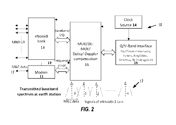
FIG. 2 is a block diagram of one embodiment of the disclosure showing the
Earth station
equipment and transmitted baseband spectrum;
FIG. 3 is a block diagram of one embodiment of the disclosure showing the non-
geo-
stationary satellite equipment and received baseband spectrum;
FIG. 4 is a flow diagram showing the up-link signal flow from the UE to the
eNodeBs; and
FIG. 5 is a flow diagram showing the downlink signal flow from the eNodeBs to
the UE.
Detailed Description
In describing the illustrative, non-limiting embodiments of the disclosure
illustrated in the
drawings, specific terminology will be resorted to for the sake of clarity.
However, the disclosure is
not intended to be limited to the specific terms so selected, and it is to be
understood that each
specific term includes all technical equivalents that operate in similar
manner to accomplish a similar
purpose. Several embodiments of the disclosure are described for illustrative
purposes, it being
understood that the disclosure may be embodied in other forms not specifically
shown in the
drawings.
Referring to the drawings, FIGS. 2, 3 show a system and method in accordance
with one non-
limiting illustrative embodiment of the present disclosure. FIG. 2 shows a
ground station having a
ground station system that includes a base station (similar to that used at a
cell tower) processing
device 13, signal delay and Doppler compensator 15, a Q/V-band interface 16,
stable clock source
14, and modem 11. The processing device 13, such as an eNodeB or bank of
eNodeBs,
communicates signals with the compensator 15, and then to the interface 16.
The eNodeB 13
transmit signals to the compensator 15, which provides delay and Doppler
compensation and has a
multiplexer to combine signals. The compensated signals are then up-converted
at the interface 16,
and transmitted to the satellite. A clock source 14 is in communication with
the eNodeB 13,
compensator 15, and interface 16 and provides a stable and accurate clocking
signal to drive
operation of the eNodeB 13, compensator 15, and interface 16.
3
CA 03165771 2022-06-22
WO 2021/145956
PCT/US2020/061532
The satellite equipment (FIG. 3) has a satellite system that includes a Q/V-
band interface 26,
multiplexer, de-multiplexer and frequency correcting processor compensator 25,
transceiver Tx/Rx
27, and modem 21. Signals from the ground station are down-converted at the
interface 26, and de-
multiplexed at the satellite compensator 25. The transceiver 27 relays the
frequency corrected
signals to User Equipment (e.g., mobile devices such as smart phones) on
earth, over a wide field-of-
view (FoV) mimicking coverage of a wide area base station. A clock source 24
is in communication
with the interface 26, satellite compensator 25, and transceiver 27 and
provides a clocking signal to
drive operation of the interface 26, compensator 25, and transceiver 27. In
the return (up-link) path,
the signals from End Users 500 are received by the transceiver 27, multiplexed
in the compensator
25 and retransmitted via the interface 26 to the gateway.
At the satellite system, the satellite modem 21 is connected to the satellite
compensator 25.
The satellite modem 21 receives monitor & control (M&C) data 23, from the Mux-
Demux of the
compensator 25 part of the ground station provides a frequency error 22 to the
frequency shifter in
the satellite compensator 25. The M&C data 23 can include data such as the
number of beams,
beam frequencies, spectral allocation, bandwidth, etc., and can be obtained
from a control center,
the eNodeB 13 or compensator 15. The frequency error is caused due to the
relative frequency error
in the clock sources 14, 24 at the gateway and the satellite and error in
predicting the location and
dynamics of the satellite (resulting in inaccurate compensation of Doppler
frequency at the
gateway). The satellite system leverages the carrier offset detection
capability of the demodulator
contained in the on-board modem 21 of M&C channel 23. The modem 21 detects the
frequency
error Af 22, the difference between the expected (based on the spectral
allocation of M&C channel)
and the observed frequency at the satellite, introduced in the signal path
from the output of the
base station 13 at ground to the output of baseband conversion 26 on the
satellite, by analyzing the
baseband signal, using carrier frequency estimation capability of the
demodulator part of the
modem, at the baseband conversion 26 to estimate the received carrierfc on the
M&C channel 23
and subtracting it the from the expected frequency ()cc) on the M&C channel
23. The purpose is to
similarly correct the frequency error in the downlink beam signals.
4
CA 03165771 2022-06-22
WO 2021/145956
PCT/US2020/061532
The de-multiplexer of the compensator 25, after separating signals for each of
the downlink
beams, applies a frequency shift that is equal to negative of the Af, before
sending them for
conversion to LTE band in the phased array 27 (e.g., a digital phased array)
and radiating the signals
to User Equipment (UE) on the ground. The phased array 27 can be, for example,
a phased array as
shown in FIG. 1 and disclosed in U.S. Patent No. 9,973,266, having a plurality
of small satellites and a
control satellite.
Likewise, in the reverse direction, the ground station modem 11 receives M&C
channel data
from control satellite via the interfaces 16 and 15.The demodulator inside the
earth station hosted
modem 11 of M&C channel estimates the frequency error 12 in the M&C channel,
by analyzing the
baseband signal at the MUX / DE-MUX 15 to estimate the received carrier fc and
subtracting it the
from the expected frequency (fc). The expected frequency is known from the M&C
data. The de-
multiplexer 15, after separating the signals received from each beam, applies
a frequency shift equal
to negative of the Af, before sending them to the eNodeBs 13 (the base-station
side of usual
terrestrial link). Thus, the base station and UE receive signals, at their
respective inputs, with same
frequency accuracy as they would receive in a usual 3GPP standards compliant
terrestrial cellular
network.
The frequency error (in both directions, ground to satellite and satellite to
ground) of the
carrier signal violates the 3GPP standard and may cause degradation or
disruption in the
communication. The frequency error occurs due to two main contributing
factors. The received
carrier frequency, f' =f + Af, for i = 0 n, where, Af is the frequency offset,
due to sum of: (a) the
difference in clock source 14 used in up/down conversions at earth station and
the clock source 24
used for up/down conversion at satellite; and (b) residual Doppler after
Doppler compensation in
the compensator 15 at the earth station. The carrier frequencyf is the carrier
frequency of the it"
signal to be sent to UE. The carrier frequencyf needs to be corrected based on
the error detected in
fc. As the satellite moves in orbit, the ground station will have a varying
delay in the signals which
results in Doppler shift. The system pre-compensates the signals that are
transmitted to the satellite
by shifting the signals in time and frequency to account for delay and Doppler
based on predicting
5
CA 03165771 2022-06-22
WO 2021/145956
PCT/US2020/061532
where the satellite will be. However, there could be residual error when the
signal reaches the
satellite. Thus, the Doppler compensation is based on predicted Doppler, but
the prediction can be
inaccurate leaving a residual error that is detected by the demodulator at the
modem 11. In one
embodiment, the frequency correction is in addition to the delay and Doppler
correction and occurs
after the delay and Doppler correction.
The Af is the same for the M&C channel and the eNodeB/UE carriers.
Accordingly, once it is
estimated by the M&C demodulator on the satellite/ground station, it is used
to correct the center
frequencies of all base station signals received from eNodeBs on ground or
signals from UEs received
via satellite. The error can be different in each direction, gateway-to-
satellite or satellite-to-gateway.
Referring to the drawings, FIGS. 4, 5 show the process explained above in the
form of signal
flow diagrams for the Uplink 30 and Downlink 70 Signal paths, respectively.
Referring to FIGS. 3, 4,
the uplink operation 30 begins at step 32, where the satellite equipment,
e.g., a beamforming
phased array 27, forms beams and collects the uplink signals from User
Equipment. These are
multiplexed, step 34, by the multiplexer of the compensator 25 along with the
M&C signal from the
modulator, step 33, of the modem 21 at an intermediate frequency IF and up-
converted by the
interface 26 to V-band frequency, step 36, and amplified and radiated by HPA
and antennas, step 38,
towards the Gateway.
Now referring to FIGS. 2, 4, the interface 16 of the gateway equipment 10
having the
Antenna and Low Noise Amplifier (LNA), collects the signals, step 52, that
were radiated from the
satellite interface 26 at step 38, for down-conversion from V-band to IF
frequency, step 54. Then the
compensator 15 de-multiplexes the uplink signals and M&C signal, step 56, and
compensates for
delay and Doppler variations, step 58. The M&C signal is received from the
satellite 20 (step 33). The
M&C signal is sent to the demodulator of the modem 11, step 57, for carrier
offset or frequency
error Af, estimation (e.g., depending on the spectral analysis resolution,
this can be a fraction of one
percent). The uplink signals are then corrected for the estimated frequency
error determined based
on the M&C signal, step 59, by the compensator 15, before they are sent to
eNodeBs 13, step 64, for
processing of the uplink signals originated at User Equipment (UE).
6
CA 03165771 2022-06-22
WO 2021/145956
PCT/US2020/061532
The downlink signal operation is shown in FIGS. 2, 5. Here, the gateway
equipment 10
comprising the eNodeBs 13, step 72, provide the downlink signals for the UE.
In parallel, the M&C
data is sent from Network Control Center, step 74, for modulation, step 75, by
the modulator of the
modem 11. The compensator 15 compensates the uplink signals and the M&C signal
for delay and
.. Doppler variations, step 73. The multiplexor of the compensator 15 then
multiplexes, step 76, the
signals to an intermediate frequency (IF). Then the interface 16 up-converts
the signals to Q-band
frequency, step 77, and amplifies and radiates the signals towards the
satellite by HPA and antenna,
step 78.
The satellite equipment 20 has an antenna and LNA to receive the signals
radiated by the
.. interface 16 at step 78. The phased array converts the Q-band signals to
IF, step 83. The signals are
de-multiplexed, step 84, by the de-multiplexer of the compensator 25. The M&C
signal is received
from the ground station 10 (step 75) is then fed to the demodulator of the
modem 21, step 85 for
carrier offset or frequency error Afd 22 estimation (e.g., depending on the
spectral analysis
resolution, this can be a fraction of one percent). Then, at the compensator
25, the downlink signals
are compensated for delay and Doppler, then corrected for the estimated
frequency error in the
monitor and control signal, step 86, before being radiated by the beamforming
phased array 27, step
88 to the UE.
The system can also be used in other communication systems in which several
channels are
multiplexed and communicated over a common radio link to correct the frequency
errors in the
signals at the receiver, by analyzing baseband signal of just one of the
channels and estimating the
its frequency error which is common to all channels.
In the embodiments shown, the small satellites 302 and/or the central
satellite 200 can
include a processing device or processing components to perform various
functions and operations
in accordance with the present disclosure, such as the operation shown in
FIGS. 4, 5. In addition, the
ground station has a processing device 13 and processing components and the
satellite has
processing components and can have a processing device. The processing devices
can be, for
instance, a computing device, processor, application specific integrated
circuits (ASIC), or controller.
7
CA 03165771 2022-06-22
WO 2021/145956
PCT/US2020/061532
The processing device can be provided with one or more of a wide variety of
components or
subsystems including, for example, wired or wireless communication links,
and/or storage device(s)
such as analog or digital memory or a database. All or parts of the system,
processes, and/or data
utilized in the system and method disclosed can be stored on or read from the
storage device. The
processing device can execute software that can be stored on the storage
device. Unless indicated
otherwise, the process is preferably implemented in automatically by the
processor substantially in
real time without delay.
It is further noted that in the embodiment of FIGS. 2-3, the system has a
demodulator to
determine frequency error, and the compensator to apply the error correction
to received signals.
However, any suitable components can be provided for determining frequency
error, such as for
example a comparator, and to apply an error correction, such as for example a
subtractor. It is
further noted that the system has standard processing communication
components, such as the Q/V
band interface, eNodeB, multiplexer and a de-multiplexer. It should be
apparent that any suitable
components can be utilized, and that those components and operation need not
be utilized. For
example, frequency error estimation can be conducted in a system that does not
include a
multiplexer, de-multiplexer, or Q/V band interface.
The foregoing description and drawings should be considered as illustrative
only of the
principles of the disclosure, which may be configured in a variety of ways and
is not intended to be
limited by the embodiment herein described. Numerous applications of the
disclosure will readily
occur to those skilled in the art. Therefore, it is not desired to limit the
disclosure to the specific
examples disclosed or the exact construction and operation shown and
described. Rather, all
suitable modifications and equivalents may be resorted to, falling within the
scope of the disclosure.
8