Note: Descriptions are shown in the official language in which they were submitted.
WO 2021/158539
PCT/US2021/016205
LIGHTNING PROTECTION SPARK GAPS FOR CABLE DEVICES
Cross-Reference to Related Applications
[0001] This patent application claims priority to U.S. Provisional Patent
Application No.
62/969,396, filed on February 3, 2020, the entirety of which is incorporated
by reference herein.
Background
[0002] A spark gap includes an arrangement of two conducting electrodes
separated by a gap
that is usually filled with a gas such as air, designed to allow an electric
spark to pass between the
conductors. When the potential difference between the conductors exceeds the
breakdown voltage
of the gas within the gap, a spark foul's, ionizing the gas and drastically
reducing its electrical
resistance. An electric current then flows until the path of ionized gas is
broken or the current
reduces below a minimum value called the "holding current." This usually
happens when the
voltage drops, but in some cases occurs when the heated gas rises, stretching
out and then breaking
the filament of ionized gas. Usually, the action of ionizing the gas is
violent and disruptive, often
leading to sound (e.g., ranging from a snap for a spark plug to thunder for a
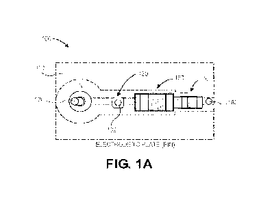
lightning discharge),
light, and heat. Spark gaps were used historically in early electrical
equipment, such as spark gap
radio transmitters, electrostatic machines, and X-ray machines. Their most
widespread use today
is in spark plugs to ignite the fuel in internal combustion engines, but they
are also used in lightning
arresters and other devices to protect electrical equipment from high-voltage
transients.
[0003] Conventional spark gaps have a low return loss and a high parasitic
capacitance. It would
be desirable to provide a spark gap that overcomes one or more of these
disadvantages.
Summary
[0004] A spark gap circuit is disclosed. The spark gap circuit includes a
circuit board. The spark
gap circuit also includes an input configured to connect to the circuit board
and to receive signals.
The spark gap circuit also includes a spark gap configured to connect to the
circuit board and the
input. The spark gap includes a first conducting electrode, a second
conducting electrode that is
grounded, and a dielectric material configured to be positioned within a gap
between the first and
second conducting electrodes. The spark gap circuit also includes a first
capacitor configured to
connect to the circuit board and the spark gap. The spark gap circuit also
includes a second
1
CA 03166201 2022- 7- 27
WO 2021/158539
PCT/US2021/016205
capacitor configured to connect to the circuit board and the first capacitor.
The spark gap circuit
also includes an output configured to connect to the circuit board and the
second capacitor. The
spark gap is configured to cause a return loss between the input and the
output to be within a first
predetermined range. The spark gap is configured to cause a parasitic
capacitance between the
input and the output to be within a second predetermined range. The first
conducting electrode
has a length from about 750 pm to about 2000 pm. The first conducting
electrode has a diameter
from about 500 m to about 1 mm. The first conducting electrode has a mass from
about 1 gram
to about 100 grams. A signal trace extends from the input to the first
capacitor. The first
conducting electrode is substantially parallel with the signal trace. The
second conducting
electrode includes a staple with two leads and a cross bar positioned
therebetween. The two leads
are substantially perpendicular to the circuit board. The cross bar is
substantially perpendicular to
the first conducting electrode and the signal trace. The cross bar is
positioned farther away from
the circuit board than the first conducting electrode such that the gap exists
therebetween. A
thickness of the gap is from about 150 pm to about 250 pm. A thickness of the
dielectric material
is from about 75 pm to about 125 pm. The dielectric material includes air,
paper, or a combination
thereof. The dielectric material has a relative permittivity from about 1 to
about 3. The first and
second capacitors are configured to block direct current (DC) flow
therethrough and to provide
surge protection. A voltage rating of the first capacitor is greater than a
voltage rating of the second
capacitor. The output is configured to connect to a cable or a device.
[0005] In another embodiment, the spark gap circuit includes a circuit board.
The spark gap
circuit also includes an input configured to connect to the circuit board and
to receive signals. The
spark gap circuit also includes a spark gap configured to connect to the
circuit board and the input.
The spark gap includes a first conducting electrode, a second conducting
electrode that is
grounded, and a dielectric material positioned within a gap between the first
and second conducting
electrodes. The spark gap circuit also includes a first capacitor configured
to connect to the circuit
board and the spark gap. The spark gap circuit also includes an output
configured to connect to
the circuit board and the first capacitor. A signal trace extends from the
input to the first capacitor.
The first conducting electrode is substantially parallel with the signal trace
The second conducting
electrode includes a staple with two leads and a cross bar positioned
therebetween. The two leads
are substantially perpendicular to the circuit board. The cross bar is
substantially perpendicular to
the first conducting electrode and the signal trace. The cross bar is
positioned farther away from
2
CA 03166201 2022- 7- 27
WO 2021/158539
PCT/US2021/016205
the circuit board than the first conducting electrode such that the gap exists
therebetween. The
spark gap is configured to cause a return loss between the input and the
output to be within a first
predetermined range. The spark gap is configured to cause a parasitic
capacitance between the
input and the output to be within a second predetermined range. The output is
configured to
connect to a cable or a device.
[0006] In yet another embodiment, the spark gap circuit includes a circuit
board. The spark gap
circuit also includes an input configured to connect to the circuit board and
to receive signals. The
spark gap circuit also includes a spark gap configured to connect to the
circuit board and the input.
The spark gap circuit also includes an output configured to connect to the
spark gap. The spark
gap is configured to cause a return loss between the input and the output to
be within a first
predetermined range. The spark gap is configured to cause a parasitic
capacitance between the
input and the output to be within a second predetermined range.
[0007] It will be appreciated that this summary is intended merely to
introduce some aspects of
the present methods, systems, and media, which are more fully described and/or
claimed below.
Accordingly, this summary is not intended to be limiting.
Brief Description of the Drawings
[0008] The accompanying drawings, which arc incorporated in and constitute a
part of this
specification, illustrate embodiments of the present teachings and together
with the description,
serve to explain the principles of the present teachings.
[0009] Figure lA illustrates a schematic view of an electrode-to-plate (pin)
spark gap circuit,
according to an embodiment.
[0010] Figure 1B illustrates a perspective view of the electrode-to-plate
(pin) spark gap circuit,
according to an embodiment.
[0011] Figure 2A illustrates a schematic view of an electrode-to-plate
(staple) spark gap circuit,
according to an embodiment.
[0012] Figure 2B illustrates a perspective view of the electrode-to-plate
(staple) spark gap
circuit, according to an embodiment.
[0013] Figure 3A illustrates a schematic view of an electrode-to-electrode
(bridged-SMT) spark
gap circuit, according to an embodiment.
3
CA 03166201 2022- 7- 27
WO 2021/158539
PCT/US2021/016205
[0014] Figure 3B illustrates a perspective view of the electrode-to-electrode
(bridged-SMT)
spark gap circuit, according to an embodiment.
[0015] Figure 4A illustrates a schematic view of an electrode-to-electrode
(bridged-SMT and
TH-ground) spark gap circuit, according to an embodiment.
[0016] Figure 4B illustrates a perspective view of the electrode-to-electrode
(bridged-SMT/ and
TH-ground) spark gap circuit, according to an embodiment.
[0017] Figure 5A illustrates a schematic view of an electrode-to-electrode
(bridged-TH) spark
gap circuit, according to an embodiment.
[0018] Figure 5B illustrates a schematic view of the electrode-to-electrode
(bridged-TH) spark
gap circuit, according to an embodiment.
[0019] Figure 6A illustrates a schematic view of a circuit with no spark gap
and no shunt
capacitor, according to an embodiment.
[0020] Figure 6B illustrates a schematic view of the circuit in Figure 6A with
no spark gap and
a shunt capacitor, according to an embodiment.
[0021] Figure 6C illustrates a schematic view of the circuit in Figure 6A with
no spark gap and
a different shunt capacitor, according to an embodiment.
[0022] Figure 7 illustrates a graph showing return loss versus effective shunt
capacitance of the
circuit shown in Figures 6A-6C, according to an embodiment.
[0023] Figure 8A illustrates a schematic view of a circuit with a spark gap
before and/or after a
surge event or surge test, according to an embodiment.
[0024] Figure 8B illustrates a schematic view of the circuit with the spark
gap during a surge
event or surge test, according to an embodiment.
[0025] Figure 9 illustrates a graph showing return loss versus effective
capacitance of a circuit
with a spark gap (e.g., the circuit in Figures 8A and 8B), before and after
electrical surge(s),
according to an embodiment.
Detailed Description
[0026] A lightning protection spark gap circuit is described herein. In one
embodiment, the
spark gap circuit may be used to protect (e.g., downstream) cable television
(CATV) circuits,
multimedia over coax alliance (MoCA) circuits, or a combination thereof.
However, as will be
appreciated, the spark gap circuit may be used to protect other types of
circuits as well. The spark
4
CA 03166201 2022- 7- 27
WO 2021/158539
PCT/US2021/016205
gap may be in one of several forms: pin, staple, bridged, or a combination
thereof. The spark
gap(s) in the circuit may be constructed of specific materials and to specific
dimensions as
described herein such that they can effectively suppress the defined surge
test criteria when they
are implemented before through-hole (TH) or surface mount technology (SMT)
series blocking
capacitors, which are rated according to the surge requirements of the port
and circuit to be
protected. The spark gap(s) are proven to meet or exceed the given test
criteria and are capable of
surviving more than 5 times the number of surge events specified.
[0027] Figure lA illustrates a schematic view of an electrode-to-plate spark
gap circuit 100, and
Figure 1B illustrates a perspective view of the electrode-to-plate spark gap
circuit 100, according
to an embodiment. The circuit 100 may include a circuit board 110 such as a
printed circuit board
(PCB). The circuit board 110 may be substantially planar. For example, the
circuit board 110
may be in an XY plane, as shown in Figure 1B.
[0028] The circuit 100 may also include an input 120 that is connected to the
circuit board 110.
The input 120 may be configured to be connected to cable or a device. In one
embodiment, the
input 120 may be configured to be connected to a CATV headend. The input 120
may be
configured to receive signals (e.g., from the CATV headend) that are in a
first bandwidth. The
first bandwidth may be from about 5 MHz to about 1002 MHz and may be referred
to as the CATV
bandwidth. The input 120 may also be configured to receive signals that arc in
a second
bandwidth. The second bandwidth may be from about 1125 MHz to about 1675 MHz
and may be
referred to as the multimedia over coax alliance (MoCA) bandwidth.
[0029] The circuit 100 may also include a spark gap 130 that is connected to
the circuit board
110 and/or the input 120. The spark gap 130 may be configured to prevent
electrical surges from
passing from the input 120 to an output 180 (discussed below), or vice versa.
The spark gap 130
may include a conducting electrode 132. In this particular embodiment, the
conducting electrode
132 is a pin. As used herein, a "pin" refers to a substantially straight wire
conductor that may be
tinned or bare (e.g., at the ends thereof where they connect to the circuit
board 110). The ends
may also be referred to as leads. The pin 132 may be made from a conductive
material such as
metal. The pin 132 may extend in a direction that is substantially
perpendicular to the circuit board
110. For example, the pin 132 may extend in a Z direction, as shown in Figure
1B. The pin 132
may extend at least partially through the circuit board 110. For example, at
least a portion of the
pin 132 may extend upward and away from an upper surface 112 of the circuit
board 110. Another
CA 03166201 2022- 7- 27
WO 2021/158539
PCT/US2021/016205
portion of the pin 132 may extend downward and away from a lower surface 114
of the circuit
board 110. The pin 132 may be connected to the circuit board 110 via a SMT
connection (e.g.,
including soldering). In another embodiment, the pin 132 may be connected to
the circuit board
110 via a TH connection that is press-fit (e.g., pin and receptacle) or
soldered.
[0030] The pin 132 may have a length from about 250 pm (-10 mil) to about 500
p.m (-20 mil),
about 500 pm to about 750 gm, about 750 pm to about 1000 pm, or more. The pin
132 may have
a cross-sectional width (diameter) that is from about 250 p.m (-10 mil) to
about 1.3 mm (-50 mil)
or about 500 pm to about 1 mm. The pin 132 may have a mass that is greater
than the mass of
conventional spark gaps. For example, the mass of the pin 132 (e.g., in the Z
direction) may be
from about 0.5 g to about 1 g, about 1 g to about 5 g, about 5 g to about 10
g, about 10 g to about
20 g, about 20 g to about 50 g, about 50 g to about 100 g, or more.
[0031] The spark gap 130 may also include a plate (also referred to as a
second conducting
electrode) 140. In one embodiment, the plate 140 may be part of a housing in
which the circuit
100 is positioned. The plate 140 may be made of a conductive material such as
metal. The plate
140 may be grounded. The plate 140 may be substantially planar. For example,
the plate 140 may
be parallel to the circuit board 110, as shown in Figure 1B. A central
longitudinal axis through the
pin 132 may be substantially perpendicular to the plate 140.
[0032] A gap may be present between an end of the pin 132 and the plate 140.
The gap may be
from about 25 t_tm (-1 mil) to about 250 t_tm (-10 mil), about 25 pm to about
50 tim, about 50 pm
to about 100 pm, about 100 pm to about 150 pm, or about 150 pm to about 250
pm. In at least
one embodiment, a dielectric material 150 may be positioned in the gap between
the end of the pin
132 and the plate 140. The dielectric material 150 may have a thickness from
about 10 pm to
about 250 pm or about 75 pm to about 125 pm. The dielectric material 150 may
have a lesser
conductance than the pin 132 and/or the plate 140. The dielectric material 150
may have a relative
permittivity (Er) from about 1 to about 3.5, from about 1 to about 2.5, or
from about 1 to about 2.
In one example, the dielectric material 150 may be air with a relative
permittivity of Er 1. In
another example, the dielectric material 150 may be paper with a relative
permittivity Er 2.3.
[0033] The circuit 100 may also include one or more capacitors (two are shown:
160, 170). The
capacitors 160, 170 may be connected to the circuit board 110 and/or the spark
gap 130. As shown,
the capacitors 160, 170 may be connected in series, with the first capacitor
160 connected to and
positioned between the spark gap 130 and the second capacitor 170. The
capacitors 160, 170 may
6
CA 03166201 2022- 7- 27
WO 2021/158539
PCT/US2021/016205
be configured to block direct current (DC) and/or to prevent surges. In at
least one embodiment,
the first capacitor 160 may have a greater voltage rating than the second
capacitor 170. For
example, the first capacitor 160 may have a voltage rating from about 200 V to
about 3000 V,
about 500 V to about 1500V, or about 750 V to about 1250 V, and the second
capacitor 170 may
have a voltage rating from about 50 V to about 2000 V, about 50 V to about 300
V, or about 50 V
to about 150 V. In one embodiment, the second capacitor 170 may be omitted.
[0034] The first capacitor 160, the second capacitor 170, or a combination
thereof may also have
a lesser voltage rating than conventional capacitors that are located
downstream of a spark gap.
This may be due to the mass of the pin 132 (being greater than most
conventional conducting
electrodes), the cross-sectional area of the pin 132 (being lesser than most
conventional conducting
electrodes), the gap width between the pin 132 and the plate 140 (being lesser
than in most
conventional spark gaps), or a combination thereof. By virtue of the
capacitors 160, 170 having a
lesser voltage rating and/or smaller size, combined with the small parallel
plate size (e.g., cross
sectional area) of the spark gap 130, the signal(s) passing through the
circuit 100 (e.g., from the
input 120 to the output 180) may experience greater return loss and/or lesser
parasitic capacitance
(through the spark gap 130) when compared to conventional circuits that
include a spark gap. For
example, the return loss of the circuit 100 may be from about 15 dB to about
40 dB, about 20 dB
to about 50 dB, or about 25 dB to about 60 dB within the first (e.g., CATV)
signal bandwidth. The
parasitic capacitance of the circuit 100 may be from about 0.01 pF to about
0.2 pF, about 0.01 pF
to about 0.1 pF, or about 0.01 pF to about 0.05 pF.
[0035] The pin(s) (e.g., pin 132) that extend through the circuit board 110
may be aligned with
the signal trace. As used herein, a "signal trace" refers to a path of the
signal (e.g., between the
input 120 and the capacitor 160). This adds substantial mass in the direction
of the Z axis, but
adds little to no width to the trace in the direction of the X axis and/or Y
axis. As a result, the pin
132 may affect (e.g., increase) the trace impedance, as measured by return
loss, from about 0.01
dB to 1 dB, about 0.1 dB to about 0.5 dB, or about 0.5 dB to about 1 dB, or
more.
[0036] As mentioned above, the circuit 100 may also include the output 180.
The output 180
may be connected to the circuit board 110 and/or the capacitor(s) 160, 170.
The output 180 may
be configured to be connect to a user premises (e.g., inside a home). For
example, the output 180
may be configured to connect to a cable and/or device such as a CATV device, a
MoCA device,
or a combination thereof.
7
CA 03166201 2022- 7- 27
WO 2021/158539
PCT/US2021/016205
[0037] Figure 2A illustrates a schematic view of another electrode-to-plate
spark gap circuit 200,
and Figure 2B illustrates a perspective view of the electrode-to-plate spark
gap circuit 200,
according to an embodiment. The circuit 200 may be similar to the circuit 100,
and similar
reference numbers are used where applicable.
[0038] Instead of, or in addition to, the spark gap 130 (from Figures lA and
1B), the circuit 200
may include a spark gap 230. The spark gap 230 may be connected to the circuit
board 110, the
input 120, the capacitors 160, 170, or a combination thereof. As shown, the
spark gap 230 is
connected to and positioned between the input 120 and the capacitor 160. The
spark gap 230 may
include a conducting electrode 232. In this particular embodiment, the
conducting electrode 232
is a staple. As used herein, a "staple" refers to a pin or wire conductor that
has at least two bends,
where the bent ends are tinned or bare to facilitate attachment to a circuit.
These end portions are
referred to as the leads, whether they are SMT or TH. Although the ends may be
soldered at the
PCT, they may not be soldered at the location of the spark gap.
[0039] The staple 232 may be made from a conductive material such as metal.
The staple 232
in Figures 2A and 2D may differ from the pin 132 in Figures lA and 1B because
it has two staple
leads, which increases the potential to achieve an initial arc and may have
about two times the
mass and cross-sectional area. The two staple leads (also referred to as pins)
234A, 234B may
extend in a direction that is substantially perpendicular to the circuit board
110. For example, the
staple leads 234A, 234B may extend in the Z direction, as shown in Figure 2B.
The staple leads
234A, 234B may extend at least partially through the circuit board 110. For
example, at least a
portion of the staple leads 234A, 234B may extend upward and away from the
upper surface 112
of the circuit board 110. Another portion of the staple leads 234A, 234B may
extend downward
and away from the lower surface 114 of the circuit board 110. The staple leads
234A, 234B may
be connected to the circuit board 110 via a SMT connection (e.g., including
soldering). In another
embodiment, the staple leads 234A, 234B may be connected to the circuit board
110 via a TH
connection that is press-fit (e.g., pin and receptacle) or soldered.
[0040] The staple 232 may also include a cross bar 236 that is connected to
(e.g., upper) ends of
the staple leads 234A, 234B. The cross bar 236 may be substantially parallel
to the circuit board
110 and substantially perpendicular to the staple leads 234A, 234B. In one
embodiment, a gap
may be present between the cross bar 236 and the circuit board 110. In another
embodiment, no
gap may be present, and the cross bar 236 may contact the circuit board 110.
8
CA 03166201 2022- 7- 27
WO 2021/158539
PCT/US2021/016205
[0041] The length of the cross bar 236 (e.g., the lateral distance between the
staple leads 234A,
234B) may be about 250 pm (-10 mil) to about 500 pm (-20 mil). The staple 232
(e.g., the staple
leads 234A, 234B, the cross bar 236, or a combination thereof) may have a
cross-sectional width
(diameter) that is from about 250 pm (-10 mil) to about 1.3 mm (-50 mil) or
about 500 pm to
about 1 mm. The staple 232 (e.g., the staple leads 234A, 234B, the cross bar
236, or a combination
thereof) may have a mass that is greater than the mass of conventional spark
gaps. For example,
the mass may be from about 0.5 g to about 1 g, about 1 g to about 5 g, about 5
g to about 10 g,
about 10 g to about 20 g, about 20 g to about 50 g, about 50 g to about 100 g,
or more.
[0042] Central longitudinal axes through the staple leads 234A, 234B may be
substantially
perpendicular to the plate 140. The gap may be present between ends of the
staple leads 234A,
234B and the plate 140. The dielectric material 150 may be positioned in the
gap between the
ends of the staple leads 234A, 234B and the plate 140. The dielectric material
150 may have the
same size, shape, and properties as described above.
[0043] The first capacitor 160, the second capacitor 170, or a combination
thereof may have a
lesser voltage rating than conventional capacitors that are located downstream
of a spark gap. This
may be due to the mass of the staple 232 (being greater than most conventional
conducting
electrodes), the cross-sectional area of the staple 232 (being lesser than
most conventional
conducting electrodes), the gap width between the staple 232 and the plate 140
(being lesser than
in most conventional spark gaps), or a combination thereof. By virtue of the
capacitors 160, 170
having a lesser voltage rating and smaller size, combined with the small
parallel plate size (e.g.,
cross sectional area) of the spark gap 230, the signal(s) passing through the
circuit 200 (e.g., from
the input 120 to the output 180) may experience greater return loss and/or
lesser parasitic
capacitance (through the spark gap 230) when compared to conventional circuits
that include a
spark gap. For example, the return loss of the circuit 200 may be from about
10 dB to about 50
dB or about 15 dB to about 40 dB within the first (e.g., CATV) signal
bandwidth. The parasitic
capacitance of the circuit 200 may be from about 0.01 pF to about 0.2 pF,
about 0.01 pF to about
0.1 pF, or about 0.01 pF to about 0.05 pF.
[0044] The cross bar 236 may be substantially parallel (e.g., aligned) with
the signal trace. This
adds substantial mass in the direction of the Z axis, but adds little to no
width to the trace in the
direction of the X axis and/or Y axis. As a result, the staple 232 may affect
(e.g., increase) the
9
CA 03166201 2022- 7- 27
WO 2021/158539
PCT/US2021/016205
trace impedance, as measured by return loss, from about 0.01 dB to 1 dB, about
0.1 dB to about
0.5 dB, or about 0.5 dB to about 1 dB, or more.
[0045] Figure 3A illustrates a schematic view of an electrode-to-electrode
spark gap circuit 300,
and Figure 3B illustrates a perspective view of the electrode-to-electrode
spark gap circuit 300,
according to an embodiment. The circuit 300 may be similar to the circuits 100
and/or 200, and
similar reference numbers are used where applicable.
[0046] Instead of, or in addition to, the spark gaps 130 and/or 230, the
circuit 300 may include
a spark gap 330. The spark gap 330 may be connected to the circuit board 110,
the input 120, the
capacitors 160, 170, or a combination thereof. As shown, the spark gap 330 is
connected to and
positioned between the input 120 and the capacitor 160. The spark gap 330 may
include bridged
surface mounted technology (SMT), as described below.
[0047] The spark gap 330 may include one or more conducting electrodes (two
arc shown: 332
and 340). In this particular embodiment, the conducting electrode 332 may be
or include a pin.
The pin 332 may be made from a conductive material such as metal. The pin 332
may be
positioned above the circuit board 110 and connected to the circuit board 110,
the input 120, the
capacitor 160, or a combination thereof via SMT. The pin 332 may extend in a
direction that is
substantially parallel to the circuit board 110, and in particular the signal
trace.
[0048] The conducting electrode 340 may be or include a staple 340. The staple
340 may be
used instead of, or in addition to, the plate 140 from the previous
embodiments. In at least one
embodiment, omitting the plate 140 may allow the circuit 300 to be self-
contained and function
without the plate 140 or housing. The staple 340 may be made of a conductive
material such as
metal. The staple 340 may be positioned above the circuit board 110 and
connected to the circuit
board 110 via SMT. At least a portion of the staple 340 may be positioned
above the dielectric
material 150 and/or the pin 332. The staple 340 may be grounded.
[0049] The staple 340 may include two staple leads (also referred to as pins)
342A, 342B that
enable the staple 340 to be mounted to the circuit board 110 via SMT. In at
least one embodiment,
the staple leads 342A, 342B may not extend through the circuit board 110. In
at least one
embodiment, the staple leads 342A, 342B may be connected (e.g., surface
mounted) to the circuit
board 110.
[0050] The staple 340 may also include a staple cross bar 344 that is
connected to (e.g., upper)
ends of the staple leads 342A, 342B. The staple cross bar 344 may be
substantially parallel to the
CA 03166201 2022- 7- 27
WO 2021/158539
PCT/US2021/016205
circuit board 110. The staple cross bar 344 may also be substantially
perpendicular to the signal
trace, the pin 332, and/or the staple leads 342A, 342B. Thus, the staple 340
(e.g., including the
staple leads 342A, 342B and the staple cross bar 344) may have the shape of a
horseshoe or the
Greek letter Omega (0).
[0051] A gap may exist between the pin 332 and the staple cross bar 344. The
gap may be from
about 25 gm (-1 mil) to about 250 gm (-10 mil), about 25 gm to about 50 gm,
about 50 gm to
about 100 gm, about 100 gm to about 150 gm, or about 150 gm to about 250 gm.
The dielectric
material 150 may be positioned in the gap between the pin 332 and the cross
bar 344. The dielectric
material 150 may have the same size, shape, and properties as described above.
[0052] The pin 332, the staple 340, or both may have a cross-sectional width
(diameter) that is
from about 250 gm (-10 mil) to about 1.3 mm (-50 mil) or about 500 gm to about
1 mm. The pin
332, the staple 340, or a combination thereof may have a mass that is greater
than the mass of
conventional spark gaps. For example, the mass may be from about 0.5 g to
about 1 2, about 1 g
to about 5 g, about 5 g to about 10 g, about 10 g to about 20 g, about 20 g to
about 50 g, about 50
g to about 100 g, or more.
[0053] The first capacitor 160, the second capacitor 170, or a combination
thereof may have a
lesser voltage rating than conventional capacitors that are located downstream
of a spark gap. This
may be due to the mass of the pin 332, the staple 340, or both (being greater
than most conventional
conducting electrodes), the cross-sectional area of the pin 332, the staple
340, or both (being lesser
than most conventional conducting electrodes), the gap width between the pin
332 and the staple
340 (being lesser than in most conventional spark gaps), or a combination
thereof. By virtue of
the capacitors 160, 170 having a lesser voltage rating and smaller size,
combined with the small
parallel plate size (e.g., cross sectional area) of the spark gap 330, the
signal(s) passing through
the circuit 300 (e.g., from the input 120 to the output 180) may experience
greater return loss
and/or lesser parasitic capacitance (through the spark gap 330) when compared
to conventional
circuits that include a spark gap. For example, the return loss of the circuit
300 may be from about
dB to about 50 dB or about 15 dB to about 40 dB within the first (e.g., CATV)
signal bandwidth.
The parasitic capacitance of the circuit 300 may be from about 0.01 pF to
about 0.2 pF, about 0.01
pF to about 0.1 pF, or about 0.01 pF to about 0.05 pF.
[0054] As mentioned above, the pin 332 may be above the circuit board 110 and
substantially
parallel (e.g., aligned) with the signal trace. The pin 332 and/or the staple
340 may add substantial
11
CA 03166201 2022- 7- 27
WO 2021/158539
PCT/US2021/016205
mass in the direction of the Z axis, but add little to no width to the trace
in the direction of the X
axis and/or Y axis. As a result, the pin 332 may and/or the staple 340 affect
(e.g., increase) the
trace impedance, as measured by return loss, from about 0.01 dB to 1 dB, about
0.1 dB to about
0.5 dB, or about 0.5 dB to about 1 dB, or more.
[0055] Figure 4A illustrates a schematic view of another electrode-to-
electrode spark gap circuit
400, and Figure 4B illustrates a perspective view of the electrode-to-
electrode spark gap circuit
400, according to an embodiment. The circuit 400 may be similar to the
circuits 100, 200, and/or
300, and similar reference numbers are used where applicable.
[0056] Instead of, or in addition to, the spark gaps 130, 230, and/or 330, the
circuit 400 may
include a spark gap 430. The spark gap 430 may be connected to the circuit
board 110, the input
120, the capacitors 160, 170, or a combination thereof. As shown, the spark
gap 430 is connected
to and positioned between the input 120 and the capacitor 160. The spark gap
430 may include
bridged SMT. For example, the pin 332 may be positioned above the circuit
board 110 and
connected to the circuit board 110, the input 120, the capacitor 160, or a
combination thereof via
SMT. In one embodiment, the pin 332 may not extend through the circuit board
110.
[0057] The circuit 400 may also include through-hole (TH) grounding. More
particularly, the
staple 440 may include two staple leads (also referred to as pins) 442A, 442B
that are configured
to extend through the circuit board 110 (e.g., in the Z direction). Lower ends
of the staple leads
442A, 442B (e.g., below the circuit board 110) may be grounded. This may
differ or improve
upon the embodiment in Figures 3A and 3B because inserting the staple leads
442A, 442B
vertically through holes in the circuit board 110 may provide alignment of the
staple leads 442A,
442B.
[0058] The first capacitor 160, the second capacitor 170, or a combination
thereof may have a
lesser voltage rating than conventional capacitors that are located downstream
of a spark gap. This
may be due to the mass of the pin 332, the staple 440, or both (being greater
than most conventional
conducting electrodes), the cross-sectional area of the pin 332, the staple
440, or both (being lesser
than most conventional conducting electrodes), the gap width between the pin
332 and the staple
440 (being lesser than in most conventional spark gaps), or a combination
thereof. By virtue of
the capacitors 160, 170 having a lesser voltage rating and smaller size,
combined with the small
parallel plate size (e.g., cross sectional area) of the spark gap 430, the
signal(s) passing through
the circuit 400 (e.g., from the input 120 to the output 180) may experience
greater return loss
12
CA 03166201 2022- 7- 27
WO 2021/158539
PCT/US2021/016205
and/or lesser parasitic capacitance (through the spark gap 430) when compared
to conventional
circuits that include a spark gap. For example, the return loss of the circuit
400 may be from about
dB to about 50 dB or about 15 dB to about 40 dB within the first (e.g., CATV)
signal bandwidth.
The parasitic capacitance of the circuit 400 may be from about 0.01 pF to
about 0.2 pF, about 0.01
pF to about 0.1 pF, or about 0.01 pF to about 0.05 pF.
[0059] As mentioned above, the pin 332 may be above the circuit board 110 and
substantially
parallel (e.g., aligned) with the signal trace. The pin 332 and/or the staple
340 may add substantial
mass in the direction of the Z axis, but add little to no width to the trace
in the direction of the X
axis and/or Y axis. As a result, the pin 332 may and/or the staple 440 affect
(e.g., increase) the
trace impedance, as measured by return loss, from about 0.01 dB to 1 dB, about
0.1 dB to about
0.5 dB, or about 0.5 dB to about 1 dB, or more.
[0060] Figure 5A illustrates a schematic view of another electrode-to-
electrode spark gap circuit
500, and Figure 5B illustrates a schematic view of the electrode-to-electrode
spark gap circuit 500,
according to an embodiment. The circuit 500 may be similar to the circuits
100, 200, 300, and/or
400, and similar reference numbers are used where applicable.
[0061] Instead of, or in addition to, the spark gaps 130, 230, 330, and/or
430, the circuit 500 may
include a spark gap 530. The spark gap 530 may be connected to the circuit
board 110, the input
120, the capacitors 160, 170, or a combination thereof. As shown, the spark
gap 530 is connected
to and positioned between the input 120 and the capacitor 160. In the spark
gap 530, the pin 332
(from Figures 3A, 3B, 4A, and 4B) may be replaced with a staple 540 that
includes staple leads
542A, 542B and a staple cross bar 544. The staple 540 and the staple 440 may
be bridged.
[0062] Rather than the staple 540 being surface mounted to the circuit board
110, the staple leads
542A, 542B may extend through the circuit board 110. This may differ or
improve upon the
embodiment in Figures 4A and 4B because inserting the staple leads 542A, 542B
vertically
through holes in the circuit board 110 may provide alignment of the staple
leads 542A, 542B. In
addition, the circuit board 110 may also include through-hole (TH) grounding.
More particularly,
the staple leads 542A, 542B may extend through the circuit board 110 (e.g., in
the Z direction).
Lower ends of the staple leads 542A, 542B (e.g., below the circuit board 110)
may be grounded.
[0063] Figure 6A illustrates a schematic view of a circuit 600 with no spark
gap and no shunt
capacitor, according to an embodiment. The circuit 600 may be similar to the
circuits 100, 200,
300, 400, and/or 500, and similar reference numbers are used where applicable.
For example, the
13
CA 03166201 2022- 7- 27
WO 2021/158539
PCT/US2021/016205
circuit 600 may include the circuit board 110, the input 120, the capacitor
(e.g., a blocking
capacitor) 160, and the output 180. The circuit 600 may also include a
resistor 610 that is
connected to the capacitor 160. The resistor 610 may be on the side of the
capacitor 160 that is
opposite to the input 120. The resistor 610 may have a resistance (e.g., 75
ohms). The resistor
610 may be grounded.
[0064] Figure 6B illustrates a schematic view of the circuit 600 with no spark
gap and a shunt
capacitor 620, according to an embodiment. A shunt capacitor 620 is connected
to the circuit 600.
More particularly, a first side of the shunt capacitor 620 is connected to and
positioned between
the input 120 and the capacitor 160. A second side of the shunt capacitor 620
may be grounded.
In this embodiment, the shunt capacitor 620 has a capacitance of 0.2 pF.
[0065] Figure 6C illustrates a schematic view of the circuit 600 with no spark
gap and a different
shunt capacitor 630, according to an embodiment. In this embodiment, the shunt
capacitor 630
has a capacitance of 0.5 p14. The circuit 600 shown in Figures 6A-6C
represents a baseline test
circuit with no spark gap.
[0066] Figure 7 illustrates a graph 700 showing return loss versus effective
shunt capacitance of
the circuit 600 shown in Figures 6A-6C, according to an embodiment. The X axis
represents
effective shunt capacitance in picofarads (pF), and the Y axis represents the
return loss at 1200
MHz in decibels (dB). The return loss is a measure of the impedance mismatch,
also known as
the reflection coefficient, and the shunt capacitance is a reactance, as
described by the following
equations:
Z = (R2 +X2) -5 Equation 1
When the capacitance increases, the impedance increases, the reflection
coefficient increases, and
the return loss decreases or degrades.
[0067] The return loss may be calculated by:
Return.Loss ¨20 id Equation 2
The reflection coeffieicnt F may be calculated by:
$2` = ¨Z
z ................... :
Li
Loati: ZO Equation 3
The impedance Z may be calculated by:
Z ......... 1.4 R jX(..?
Equation 4
The capacitance reactance Xc may be calculated by:
14
CA 03166201 2022- 7- 27
WO 2021/158539
PCT/US2021/016205
1
Xt.7 ......... ¨
coe 2-RIC Equation 5
In these equations, F = frequency, C = capacitance, R = Real component, X =
Reactive component,
Z = circuit impedance, and Zo ¨ Nominal impedance (e.g., 75 ohms).
[0068] The bottom line 710 represents results for when the capacitor 160 is a
disc with a 1 kV
rating. The middle line 720 represents results for when the capacitor 160 is a
disc with a 500 V
rating. The top line 730 represents results for when the capacitor 160 is a
multilayer ceramic
capacitor (MLCC) with a 2 kV rating.
[0069] Figure 8A illustrates a schematic view of a circuit 800 with a spark
gap 810, before and/or
after a surge event or surge test. and Figure 8B illustrates a schematic view
of the circuit 800 with
the spark gap 810 during a surge event or surge test, according to an
embodiment. The circuit 800
may be similar to the circuits 100, 200, 300, 400, 500 and/or 600, and similar
reference numbers
are used where applicable. For example, the circuit 800 may include the
circuit board 110, the
input 120, the capacitor (e.g., a blocking capacitor) 160, the output 180, and
the resistor 610.
[0070] The circuit 800 may also include the spark gap 820. A first side of the
spark gap 820
may be connected to and positioned between the input 120 and the capacitor
160. The second side
of the spark gap 820 may be grounded. The spark gap 820 may be or include any
of the spark gaps
130, 230, 330, 430, 530 discussed above. For example, the spark gap 820 may
include two
conducting electrodes (e.g., electrodes 332 and 340) that are crossed (e.g.,
bridged). The electrodes
may be made of tinned copper wire and have a cross-sectional width (e.g.,
diameter) of about 635
m (i.e., ¨25 mil). The dielectric material 150 may be paper having a thickness
of about 89 m
(i.e., ¨3.5 mil).
[0071] Figure 9 illustrates a graph 900 showing return loss versus effective
capacitance of the
circuit 800 before and after an electrical surge, according to an embodiment.
The graphs 700, 900
may be compared to illustrate the performance of a circuit (e.g., circuit 800)
with a spark gap over
the baseline performance of a circuit (e.g., circuit 600) without a spark gap.
[0072] The bottom line 910 represents results when the capacitor 160 is a disc
with a 1 kV rating.
As shown at point 912, before the surge test, the return loss is -12.1 when
the effective capacitance
is 0.13 pF. At point 914, after the surge test, the return loss is -11.9 when
the effective capacitance
is 0.15 pF. The middle line 920 represents results when the capacitor 160 is a
disc with a 500 V
rating. As shown at point 922, before the surge test, the return loss is -13.4
when the effective
CA 03166201 2022- 7- 27
WO 2021/158539
PCT/US2021/016205
capacitance is 0.08 pF. At point 924, after the surge test, the return loss is
-13.3 when the effective
capacitance is 0.09 pF. The top line 930 represents results when the capacitor
160 is a multilayer
ceramic capacitor (MLCC) with a 2 kV rating. As shown at point 932, before the
surge test, the
return loss is -14.5 when the effective capacitance is 0.13 pF. At point 934,
after the surge test,
the return loss is -14.2 when the effective capacitance is 0.18 pF.
[0073] The return loss measurements are taken with a shunt capacitance of an
891..tm (i.e., ¨3.5
mil) introduced by a bridged spark gap (e.g., spark gap 330, 430, or 530), a
high voltage blocking
capacitor 160 (e.g., with a voltage rating of 500 V, 1 kV, or 2 kV), and a 75-
ohm termination
resistor. The surge measurements were taken with a shunt capacitance of an 89
i.tm (i.e., ¨3.5 mil)
introduced by a bridged spark gap (e.g., spark gap 330, 430, or 530), a high
voltage blocking
capacitor 160 (e.g., with a voltage rating of 500 V, 1 kV, or 2 kV), and a
short to ground.
[0074] Table 1 below includes the spark gap performance characteristics and
the performance
target(s) for the circuit 800, according to an embodiment.
Table 1
Spark Gap Performance Characteristics Performance
Target
Effective Shunt
About 0.1 pF < 0.2 pF
Capacitance
Post Surge Capacitance
0.05 pF < 0.1 pF
Change
Initial Arc Voltage 1250V 250V <2 KV
Surge Withstand Event 1/2 samples > 50 (test halted) > 96 (3x the
SCTE 32 Step
Count 1/2 samples > 96 (test halted) Standard)
> 915 Mega Watts
Surge Withstand >= 915 MW (3x the SCTE 32 Step
(Instantaneous sum not
Power Dissipation Standard)
actual total which is greater)
Blocking Capacitors
2KV 1206 MLCC
Acceptable Type &
500V & 1KV Ceramic Disc
Ratings
In this test, the surge events were halted without circuit damage after 50
events in most cases when
the instantaneous sum power dissipation met or exceeded three times that of
the surge test standard:
IEEE C 62.41 Category B3 Combination Waveform as specified by SCTE 81.
Exposing various
test samples to only 50 surge events implemented at a set higher 6 KV 3KA
level met or exceeded
the 96 stepped events defined in the standard because the power dissipation
was met or exceeded
and confirmed by splitting the samples tested with stepped or set event
levels.
16
CA 03166201 2022- 7- 27
WO 2021/158539
PCT/US2021/016205
[0075] As may be seen, the spark gaps 130, 230, 330, 430, 530 have a
relatively low capacitance,
have a low impact on circuit return loss, and are robust or they have a high
surge withstand and
life. The MLCC capacitor 160 adds more inherent capacitance to the circuit
800. The 1 kV disc
capacitor 160 adds less inherent capacitance to the circuit 800. The disc
capacitors perform greater
than 2x their voltage rating. The tinned copper wires (e.g., pins or staples
332, 340, 440, 540)
erode as a result of the testing, which increases the gap size therebetween.
The tinned copper wires
have a cross-sectional width (e.g., diameter) from about 381 p.m (i.e., -15
mil) to about 1016 pna
(i.e., -40 mil). This may lower the capacitance, but the capacitance of the
circuit 800 may increase
due to conductive carbon residue from the testing. The testing resulted in a
low initial arc voltage
and range from about 1250 V AI- 250 V. The circuit 800 is robust and can
withstand greater than
3x the SCTE standard. The dielectric material 150 may be paper, which provides
a low and
consistent arc voltage due to more consistent gapping during assembly.
[0076] In one embodiment, a lightning protection spark gap circuit for a CAIN
line and/or a
drop device is disclosed. The spark gap circuit may include low initial arc
voltage, low parasitic
capacitance or intrinsic reactance, low cost, ease of manufacture, robust
life, and consistent
performance. The spark gap circuit may be validated by the Institute of
Electrical and Electronics
Engineers (IEEE) C 62.41 Category 113 combination waveform as specified by the
Society of
Cable Telecommunications Engineers (SCTE) 81 2012. The spark gap circuit may
be configured
to operate through a 6 kV, 3 kA. 2 ohm standard 1.2/50 tS - 8/20 u.S combo
wave surge. The
spark gap circuit may also operate at this level through at least 32
incremental events.
[0077] In another embodiment, the spark gap circuit may be validated by the
IEEE C 62.41
Category B3 ring waveform as specified by the SCTE 81 2012. The spark gap
circuit may be
configured to operate through a 6 kV, 500 A, 12 ohm standard 0.51aS ring wave
surge. The spark
gap circuit may be configured to operate at this level through at least 32
incremental events.
[0078] In another embodiment, the spark gap circuit may be validated by the
IEEE C 62.41
Category A3 ring waveform as specified by the SCTE 81 2012. The spark gap
circuit may be
configured to operate through a 6 kV, 200 A, 30 ohm standard 0.51.1.S ring
wave surge. The spark
gap circuit may be configured to operate at this level through at least 32
incremental events.
[0079] The spark gap circuits on a printed circuit board (PCB) may be followed
by series
blocking capacitance characterized by surface mount technology (SMT) 1206 2 kV
followed by
17
CA 03166201 2022- 7- 27
WO 2021/158539
PCT/US2021/016205
0805 100 V or greater; TH 1 kV or greater, SMT 1206 ikV or greater (e.g., for
A3 ring only), TH
200 V or greater (e.g., for A3 ring only), or a combination thereof.
[0080] In one embodiment, the spark gap circuit may be or include a planer
spark gap circuit on
a PCB that includes a base conductor material (e.g., 1 ounce of copper). The
planer spark gap
circuit may also include a hot air solder leveling (HASL) plating to increase
mass in the Z axis.
The planer spark gap circuit may also include a gap between two or more
electrodes that is from
about 3.5 mil to about 6.5 mil. The planer spark gap circuit may also include
an electrode
separation from about 10 mil to about 20 mil. The planer spark gap circuit may
also include an
electrode geometry that is, for example, blunt to blunt. This may include a
tip that is from about
mil to about 10 mil, and a length from the conductor or ground that is from
about 5 mil to about
mil. The planer spark gap circuit may also include a conductor and ground mass
that is greater
than about 50x20 mil for a ring wave and/or greater than about 150x50 mil for
a combo wave. The
planer spark gap circuit may also include plated through holes that may be
configured to increase
mass either unfilled or solder filled (e.g., for a combo wave).
[0081] In another embodiment, the spark gap circuit may be or include a bridge
spark gap circuit
on a PCB that includes an electrode cross-section that is from about 10 mil to
about 40 mil in
diameter (or equivalent cross sectional area in other geometries). The bridge
spark gap circuit may
also include an electrode length that is greater than about 30 mil. The bridge
spark gap circuit may
also include an electrode orientation that is about 90 degrees (e.g.,
perpendicular) from the
conductor to ground. The bridge spark gap circuit may also include a single
electrode or multiple
electrodes for ground. The bridge spark gap circuit may also include multiple
electrodes that may
be separated by air or another dielectric material (e.g., gas) that is from
about 3 mil to about 5 mil
thick. The bridge spark gap circuit may also include a gap dielectric constant
that is less than about
3.5 (e.g., paper at 2.3).
[0082] In another embodiment, the spark gap circuit may be or include a staple
or pin spark gap
circuit on a PCB that includes an electrode diameter from about 10 mil to
about 40 mil (or
equivalent cross sectional area in other geometries). The staple or pin spark
gap circuit may also
include an electrode length that is greater than about 30 mil. The staple or
pin spark gap circuit
may also include an electrode orientation that is about 90 degrees (e.g.,
perpendicular) from the
conductor to ground. The staple or pin spark gap circuit may also include
multiple electrodes in
line with the conductor. The staple or pin spark gap circuit may also include
one or more electrodes
18
CA 03166201 2022- 7- 27
WO 2021/158539
PCT/US2021/016205
that is/are perpendicular to ground. The staple or pin spark gap circuit may
also include one or
more electrodes that are separated from ground by air or another dielectric
material (e.g., gas) that
is from about 3 mil to about 5 mil thick. The bridge spark gap circuit may
also include a gap
dielectric constant that is less than about 3.5 (e.g., paper).
[0083] While various aspects and embodiments have been disclosed herein, other
aspects and
embodiments will be apparent to those skilled in the art. The various aspects
and embodiments
disclosed herein are for purposes of illustration and are not intended to be
limiting, with the true
scope and spirit being indicated by the following claims. The present
disclosure is not to be limited
in temis of the particular embodiments described in this application, which
are intended as
illustrations of various aspects. Many modifications and variations can be
made without departing
from its spirit and scope, as will be apparent to those skilled in the art.
Functionally equivalent
apparatuses within the scope of the disclosure, in addition to those
enumerated herein will be
apparent to those skilled in the art from the foregoing descriptions. Such
modifications and
variations are intended to fall within the scope of the appended claims. The
present disclosure is
to be limited only by the terms of the appended claims, along with the full
scope of equivalents to
which such claims are entitled. It is also to be understood that the
terminology used herein is for
the purpose of describing particular embodiments only, and is not intended to
be limiting.
[0084] With respect to the use of substantially any plural and/or singular
terms herein, those
having skill in the art can translate from the plural to the singular and/or
from the singular to the
plural as is appropriate to the context and/or application. The various
singular/plural permutations
may be expressly set forth herein for sake of clarity.
[0085] It will be understood by those within the art that, in general, terms
used herein, and
especially in the appended claims (e.g., bodies of the appended claims) are
generally intended as
"open" terms (e.g., the tel __ la "including" should be interpreted as
"including but not limited to,"
the term "having" should be interpreted as "having at least," the term
"includes" should be
interpreted as "includes but is not limited to," etc.). It will be further
understood by those within
the art that if a specific number of an introduced claim recitation is
intended, such an intent will
be explicitly recited in the claim, and in the absence of such recitation no
such intent is present.
For example, as an aid to understanding, the following appended claims may
contain usage of the
introductory phrases "at least one" and "one or more" to introduce claim
recitations. However,
the use of such phrases should not be construed to imply that the introduction
of a claim recitation
19
CA 03166201 2022- 7- 27
WO 2021/158539
PCT/US2021/016205
by the indefinite articles "a" or "an limits any particular claim containing
such introduced claim
recitation to embodiments containing only one such recitation, even when the
same claim includes
the introductory phrases "one or more" or "at least one" and indefinite
articles such as "a" or "an"
(e.g., "a" and/or "an" should be interpreted to mean "at least one" or "one or
more"); the same
holds true for the use of definite articles used to introduce claim
recitations. In addition, even if a
specific number of an introduced claim recitation is explicitly recited, those
skilled in the art will
recognize that such recitation should be interpreted to mean at least the
recited number (e.g., the
bare recitation of "two recitations," without other modifiers, means at least
two recitations, or two
or more recitations). Furthermore, in those instances where a convention
analogous to "at least
one of A, B, and C, etc." is used, in general such a construction is intended
in the sense one having
skill in the art would understand the convention (e.g., "a system having at
least one of A, B, and
C" would include but not be limited to systems that have A alone, B alone, C
alone, A and B
together, A and C together, B and C together, and/or A, B, and C together,
etc.). In those instances
where a convention analogous to "at least one of A, B, or C, etc." is used, in
general such a
construction is intended in the sense one having skill in the art would
understand the convention
(e.g., "a system having at least one of A, B, or C" would include but not be
limited to systems that
have A alone, B alone, C alone, A and B together, A and C together, B and C
together, and/or A,
B, and C together, etc.). It will be further understood by those within the
art that virtually any
disjunctive word and/or phrase presenting two or more alternative terms,
whether in the
description, claims, or drawings, should be understood to contemplate the
possibilities of including
one of the terms, either of the terms, or both terms. For example, the phrase
"A or B" will be
understood to include the possibilities of "A" or "B- or "A and B." In
addition, where features or
aspects of the disclosure are described in terms of Markush groups, those
skilled in the art will
recognize that the disclosure is also thereby described in terms of any
individual member or
subgroup of members of the Markush group.
CA 03166201 2022- 7- 27