Note: Descriptions are shown in the official language in which they were submitted.
WO 2021/186257
PCT/IB2021/050660
AUGMENTED SEMICONDUCTOR LASERS WITH SPONTANEOUS EMISSIONS BLOCKAGE
BACKGROUND OF THE INVENTION
[0001] The present invention relates generally to semiconductor lasers, and
more particularly, to semiconductor
lasers with spontaneous emissions blockage.
[0002] Semiconductor lasers such as conventional edge-emitting laser, also
known as laser-diodes or vertical-cavity
surface-emitting lasers (VCSELs) are commercially used in a very wide range of
applications: Displays and
illumination, data storage, communication, data reading, data recording,
defense, laser printing, medical and cosmetic
applications, material processing such as surface treatment, optical pumping
sources and more.
[0003] When increasing the electrical power, typical semiconductor lasers
transition between two different states at a
given threshold current (14
= spontaneous emission state which occurs below a threshold, to produce
incoherent emission, randomized
polarization, randomized phase, randomized emission direction, broad beam
width; and
= stimulated emission state, which occurs above a power threshold, to
produce laser operation characterized by
coherent emission with identical photon energy, narrow line width, identical
photon direction, identical photon phase or
temporal coherence and identical photon polarization or coherently polarized
light.
SUMMARY OF THE INVENTION
[0004] In one embodiment, shown is a device and a method to produce an
augmented-Laser (ATLAS) comprising a
bi-stable resistive system (BRS) integrated in series with a semiconductor
laser. ATLAS exhibits reduction/inhibition of
the Spontaneous Emission (SE) below lasing threshold by leveraging the abrupt
resistance switch of the BRS.
[0005] In one embodiment, a laser system comprises a semiconductor laser and a
bi-stable resistive system (BRS)
operates as a reversible switch. The BRS is electrically connected in series
with the semiconductor laser. The BRS
operates in a high resistive state in which a semiconductor laser is below a
lasing threshold and emitting in a
spontaneous emission regime, and a low resistive state in which a
semiconductor laser is above or equal to a lasing
threshold and emitting in a stimulated emission regime. The BRS operating as a
reversible switch is electrically
connected in series across two independent chips or on a single wafer. The BRS
is formed using insulator-to-metal
transition (I MT) materials or is formed using threshold-switching selectors
(TSS).
1
CA 03166664 2022- 7- 30
WO 2021/186257
PCT/1B2021/050660
[0006] In another embodiment a vertical wave guide laser semiconductor device
comprises a semiconductor
substrate, and a layer structure formed thereon with a quantization axis of an
active medium layer that is in parallel with
a vertical axis of an optical cavity. The layer structure includes a first
wave guide layer with a first doping type disposed
over a semiconductor substrate, the active medium layer disposed over the
first wave guide layer, and a second wave
guide layer with a second doping type and an oxidation layer disposed over the
active medium layer. A mesa type
structure with a top surface and a side wall is formed from the first wave
guide layer. The active medium layer and the
second wave guide layer and an aperture formed in the second wave guide layer.
A bi-stable resistive system (BRS) is
formed: i) on the first wave guide layer around the mesa type structure or ii)
on the top surface of the mesa type
structure.
[0007] In one embodiment the layer structure is a vertical-cavity surface-
emitting laser (VSCEL) and the BRS is
formed using insulator-to-metal transition (IMT) materials or formed using
threshold-switching selectors.
[0008] In another embodiment a vertical wave guide laser semiconductor device
comprises a semiconductor
substrate, and a layer structure formed thereon with a quantization axis of an
active medium layer that is in parallel with
a vertical axis of an optical cavity. The layer structure including a first
wave guide layer with a first doping type
disposed over a semiconductor substrate, the active medium layer disposed over
the first wave guide layer, and a
second wave guide layer with a second doping type and an oxidation layer
disposed over the active medium layer. Aa
mesa type structure with a top surface and a side wall formed from the first
wave guide layer, the active medium layer,
and the second wave guide layer and an aperture formed in the second wave
guide layer. A bi-stable resistive system
(BRS) formed on a back side of the semiconductor substrate with a first
contact layer formed over the bi-stable
resistive system; and a second contact layer formed over the second wave guide
layer and having an opening over the
aperture, the second contact layer is electrically isolated from the first
contact layer. The bi-stable resistive system is
formed using insulator-to-metal transition (IMT) materials or a threshold-
switching selectors (TSS).
[0009] An edge-emitting laser semiconductor device comprises a semiconductor
substrate, and a layer structure
formed thereon. The layer structure including a first cladding layer with a
first doping type disposed over a top side of a
semiconductor substrate; a first wave guide layer disposed over the first
cladding layer, an active medium layer with
multiple quantum wells disposed over the first wave guide layer, a second wave
guide layer disposed over the active
medium layer, and a second cladding layer with a second doping type disposed
over the second wave guide layer. A
mesa type structure is formed with a top surface and a side wall from the
second cladding layer. An oxide layer is
formed on either side of the mesa type structure. A bi-stable resistive system
(BRS) formed i) on the top surface of the
mesa type structure with a first contact layer formed thereon and a second
contact layer formed on a bottom side of the
semiconductor substrate, or ii) on a back side of the semiconductor substrate
with a first contact layer formed thereon
and a second contact layer formed on the top surface of the mesa type
structure. The bi-stable resistive system is
formed using insulator-to-metal transition (IMT) materials or a threshold-
switching selectors (TSS).
2
CA 03166664 2022- 7- 30
WO 2021/186257
PCT/1B2021/050660
[0010] In another embodiment, a vertical wave guide laser semiconductor device
comprises a semiconductor
substrate, and a layer structure formed thereon with an quantization axis of
an active medium layer that is in parallel
with a vertical axis of an optical cavity. The layer structure including a
first wave guide layer with a first doping type
disposed over a semiconductor substrate, the active medium layer disposed over
the first wave guide layer, and a
second wave guide layer with a second doping type and an oxidation layer
disposed over the active medium layer, with
at last one layer of a bi-stable resistive system (BRS) formed i) within the
active medium layer or ii) within the second
wave guide layer; and a mesa type structure with a top surface and a side wall
formed from the first wave guide layer,
the active medium layer and the second wave guide layer and an aperture formed
in the second wave guide layer. The
bi-stable resistive system is formed using insulator-to-metal transition (IMT)
materials or a threshold-switching selectors
(TSS). The vertical wave guide laser in one example is a vertical-cavity
surface-emitting laser (VSCEL) and the bi-
stable resistive system is formed using insulator-to-metal transition (I MT)
materials or threshold-switching selectors
(TSS).
BRIEF DESCRIPTION OF THE DRAWINGS
[0011] The accompanying figures where like reference numerals refer to
identical or functionally similar elements
throughout the separate views, and which together with the detailed
description below are incorporated in and form part
of the specification, serve to further illustrate various embodiments and to
explain various principles and advantages all
in accordance with the present invention, in which:
[0012] FIG. 1 illustrates a graph of basic operating of a laser of FIG. 1 with
respect to pumping current, according to
the prior art;
[0013] FIG. 2 illustrate a graph of current versus voltage characteristic of a
bi-stable resistive system, according to
the prior art;
[0014] FIG. 3 is a graph of output optical power versus pumping current of a
classical laser, according to the prior art;
[0015] FIG. 4 is a graph of output optical power versus pumping current of an
augmented laser using a bi-stable
system, according to one embodiment of the present invention;
[0016] FIG. 5A and FIG. 5B are an illustration of an augmented laser switching
reversibly between an OFF-state and
an ON-state associated with a high resistive state (HRS) and a low resistive
state (LRS) of the bi-stable resistive
system respectively, according to one embodiment of the present invention;
[0017] FIG. 6 is a series of graphs of output optical power versus pumping
current for various configurations of an
augmented laser with bi-stable resistive system, according to one embodiment
of the present invention;
[0018] FIG. 7 is a series of graphs of output optical power versus pumping
current for various configurations of an
augmented laser with bi-stable resistive system exhibit small or non-existent
hysteresis as compared to compared to
the hysteresis in FIG. 6, according to one embodiment of the present
invention;
3
CA 03166664 2022- 7- 30
WO 2021/186257
PCT/1B2021/050660
[0019] FIG. 8 is a side view illustrating an initial stage in formation
of a vertical cavity surface emitting laser
semiconductor device with an integrated bi-stable resistive system, according
to one embodiment of the present
invention;
[0020] FIG. 9A is a top perspective view and FIG. 9B is a corresponding cross-
sectional view taken along line X-X'
illustrating a later stage in forming the vertical cavity surface emitting
laser semiconductor device of FIG. 8 with a bi-
stable resistive system integrated on buried bottom contact, according to one
embodiment of the present invention;
[0021] FIG. 10 is a cross-sectional view taken along line X-X' illustrating a
later stage in forming the vertical cavity
surface emitting laser semiconductor device of FIG. 8 with a bi-stable
resistive system integrated on a top contact,
according to one embodiment of the present invention;
[0022] FIG. 11 is a cross-sectional view taken along line X-X' illustrating a
later stage in forming the vertical cavity
surface emitting laser semiconductor device of FIG. 8 with a bi-stable
resistive system integrated on a back-side
contact, according to one embodiment of the present invention;
[0023] FIG. 12 is a flow diagram illustrating one example of a process for
forming a vertical cavity surface emitting
laser semiconductor device with an integrated bi-stable resistive system
according to one embodiment of the present
invention;
[0024] FIG. 13A is a top perspective view and FIG. 13B is a corresponding
cross-sectional view taken along line X-X'
illustrating an initial stage in formation of an edge emitting semiconductor
laser or diode device with an integrated bi-
stable resistive system, according to one embodiment of the present invention;
[0025] FIG. 14A and 14B are schematic cross-sectional views taken along X-X'
line and Y-Y' line respectively
illustrating a later stage in forming the edge emitting semiconductor laser or
diode device of FIG.13B with a bi-stable
resistive system integrated on a top contact, according to one embodiment of
the present invention;
[0026] FIG. 15 is a schematic cross-sectional view illustrating a later stage
in forming the edge emitting
semiconductor laser or diode device of FIG.13B with a bi-stable resistive
system integrated on a back-side contact,
according to one embodiment of the present invention;
[0027] FIG. 16 is a schematic side view illustrating a semiconductor laser
device with a bi-stable resistive system
integrated within the active medium of the laser, according to one embodiment
of the present invention;
[0028] FIG. 17 is schematic cross-sectional view taken along line X-X'
illustrating the formation of a vertical cavity
surface emitting laser semiconductor device with a bi-stable resistive system
integrated within the active medium of the
device, according to one embodiment of the present invention;
[0029] FIG. 18 is a schematic side view illustrating a semiconductor laser
device with a bi-stable resistive system
integrated within the waveguide of the laser optical cavity, according to one
embodiment of the present invention;
[0030] FIG. 19 is schematic cross-sectional view taken along line X-X'
illustrating the formation of a vertical cavity
surface emitting laser semiconductor device with a bi-stable resistive system
integrated within the waveguide of the
laser optical cavity, according to one embodiment of the present invention;
and
[0031] FIG. 20 is a flow diagram illustrating one example of a process for
forming a laser semiconductor device with
a bi-stable resistive system inside the active medium or waveguide of the
laser, according to one embodiment of the
present invention.
4
CA 03166664 2022- 7- 30
WO 2021/186257
PCT/1B2021/050660
DETAILED DESCRIPTION
Non-Limiting Review of Semiconductor Device Descriptions
[0032] It is to be understood that the various layers and/or regions shown in
the accompanying drawings are not
drawn to scale, and that one or more layers and/or regions of a type commonly
used in laser semiconductor and/or
other semiconductor devices may not be explicitly shown in a given drawing.
This does not imply that the layers and/or
regions not explicitly shown are omitted from the actual devices. In addition,
certain elements may be left out of
particular views for the sake of clarity and/or simplicity when explanations
are not necessarily focused on the omitted
elements. Moreover, the same or similar reference numbers used throughout the
drawings are used to denote the
same or similar features, elements, or structures, and thus, a detailed
explanation of the same or similar features,
elements, or structures will not be repeated for each of the drawings.
[0033] The semiconductor devices and methods for forming same in accordance
with various embodiments of the
present invention may be employed in applications, hardware, and/or electronic
systems. Suitable hardware and
systems for implementing embodiments of the invention may include, but are not
limited to, personal computers,
communication networks, electronic commerce systems, portable communications
devices (e.g., cell and smart
phones), solid-state media storage devices, functional circuitry, etc. Systems
and hardware incorporating the
semiconductor devices are contemplated embodiments of the invention. Given the
teachings of embodiments of the
invention provided herein, one of ordinary skill in the art will be able to
contemplate other implementations and
applications of embodiments of the invention.
[0034] As used herein, "vertical" refers to a direction perpendicular to a
substrate in the views herein. As used
herein, "horizontal" refers to a direction parallel to a substrate views
herein. As used herein, "thickness" refers to a size
of an element (e.g., a layer, trench, hole, etc.) in the cross-sectional views
measured from a bottom surface to a top
surface, or a left side surface to a right side surface of the element, and/or
measured with respect to a surface on which
the element is directly on.
[0035] Unless otherwise specified, as used herein, "height" or "height above a
substrate" refers to a vertical size of an
element (e.g., a layer, trench, hole, etc.) in the cross-sectional views
measured from a top surface of the substrate to a
top surface of the element. A thickness of an element can be equal to a height
of the element if the element is directly
on the substrate. As used herein, "lateral", "lateral side", and "lateral
surface", and the like, refer to a side surface of an
element (e.g., a layer, an opening, a fin, etc.), such as a left or right side
surface in the cross-sectional views herein.
[0036] As used herein, the terms "width" or "width value", and the like, refer
to a distance from a start point on a first
structure to an end point on the same structure, in a critical dimension.
There can be specified a vertical width (e.g., a
thickness) of the structure or a horizontal width of the structure.
CA 03166664 2022- 7- 30
WO 2021/186257
PCT/1B2021/050660
[0037] It will also be understood that when an element such as a layer, region
or substrate is referred to as being "on"
or "over another element, it can be directly on the other element or
intervening elements may also be present. Similar
but inverse meaning will be understood for an element such as a layer, region,
or substrate that is referred to as being
"under" or "below" another element. It can be directly under the other element
or intervening elements may also be
present. In contrast, when an element is referred to as being "directly on" or
"directly over", or alternatively referred to
as being "directly under" or "directly below" another element, there are no
intervening elements present. It will also be
understood that when an element is referred to as being "connected" or
"coupled" to another element, it can be directly
connected or coupled to the other element or intervening elements may be
present. In contrast, when an element is
referred to as being "directly connected" or "directly coupled" to another
element, there are no intervening elements
present.
[0038] The present invention may include a design for an integrated circuit
chip, which may be created in a graphical
computer programming language, and stored in a computer storage medium (such
as a disk, tape, physical hard drive,
or virtual hard drive such as in a storage access network). If the designer
does not fabricate chips or the
photolithographic masks used to fabricate chips, the designer may transmit the
resulting design by physical means
(e.g., by providing a copy of the storage medium storing the design) or
electronically (e.g., through the Internet) to such
entities, directly or indirectly. The stored design is then converted into the
appropriate format (e.g., GDSII) for the
fabrication of photolithographic masks, which typically include multiple
copies of the chip design in question that are to
be formed on a wafer. The photolithographic masks are utilized to define areas
of the wafer (and/or the layers thereon)
to be etched or otherwise processed.
[0039] Methods as described herein may be used in the fabrication of
integrated circuit chips. The resulting
integrated circuit chips can be distributed by the fabricator in raw wafer
form (that is, as a single wafer that has multiple
unpackaged chips), as a bare die, or in a packaged form. In the latter case
the chip is mounted in a single chip
package (such as a plastic carrier, with leads that are affixed to a
motherboard or other higher-level carrier) or in a
multichip package (such as a ceramic carrier that has either or both surface
interconnections or buried
interconnections). In any case the chip is then integrated with other chips,
discrete circuit elements, and/or other signal
processing devices as part of either (a) an intermediate product, such as a
motherboard, or (b) an end product. The
end product can be any product that includes integrated circuit chips, ranging
from toys and other low-end applications
to advanced computer products having a display, a keyboard or other input
device, and a central processor.
[0040] Reference in the specification to "one embodiment" or 'an embodiment"
of the present principles, as well as
other variations thereof, means that a particular feature, structure,
characteristic, and so forth described in connection
with the embodiment is included in at least one embodiment of the present
principles. Thus, the appearances of the
phrase in one embodiment" or "in an embodiment", as well any other variations,
appearing in various places
throughout the specification are not necessarily all referring to the same
embodiment.
6
CA 03166664 2022- 7- 30
WO 2021/186257
PCT/1B2021/050660
[0041] It is to be understood that the various layers and/or regions shown in
the accompanying drawings are not
drawn to scale, and that one or more layers and/or regions of semiconductor
lasers may not be explicitly shown in a
given drawing. This does not imply that the layers and/or regions not
explicitly shown are omitted from the actual
devices. In addition, certain elements may be left out of particular views for
the sake of clarity and/or simplicity when
explanations are not necessarily focused on the omitted elements. Moreover,
the same or similar reference numbers
used throughout the drawings are used to denote the same or similar features,
elements, or structures, and thus, a
detailed explanation of the same or similar features, elements, or structures
will not be repeated for each of the
drawings.
[0042] Deposition may be by any process that grows, coats, or otherwise
transfers a material onto the wafer.
Available technologies include, for example, physical vapor deposition (PvD),
chemical vapor deposition (CVD),
electrochemical deposition (ECD), molecular beam epitaxy (MBE) and more
recently, atomic layer deposition (ALD)
among others.
[0043] The terms "epitaxially growing", "epitaxial growth", "epitaxially
grown", and their variants, mean the growth of a
semiconductor material on a deposition surface of a semiconductor material, in
which the semiconductor material being
grown has the same crystalline characteristics as the semiconductor material
of the deposition surface. In an epitaxial
deposition process, the chemical reactants provided by the source gases are
controlled and the system parameters are
set so that the depositing atoms arrive at the deposition surface of the
semiconductor substrate with sufficient energy to
move around on the surface and orient themselves to the crystal arrangement of
the atoms of the deposition surface.
Therefore, an epitaxial semiconductor material has the same crystalline
characteristics as the deposition surface on
which it is formed. For example, an epitaxial semiconductor material deposited
on a {100} crystal surface will take on a
{100} orientation. In some embodiments, epitaxial growth and/or deposition
processes are selective to forming on
semiconductor surface, and do not deposit material on dielectric surfaces,
such as silicon dioxide or silicon nitride
surfaces.
[0044] Examples of various epitaxial growth process apparatus that are
suitable for use in one or more embodiments
include, e.g., rapid thermal chemical vapor deposition (RTCVD), low-energy
plasma deposition (LEPD), ultra-high
vacuum chemical vapor deposition (UHVCVD), atmospheric pressure chemical vapor
deposition (APCVD) and
molecular beam epitaxy (MBE). A number of different sources can be used for
the deposition of the various layers
discussed herein. For example, the gas source for the deposition of epitaxial
semiconductor material can include a
silicon containing gas source, a germanium containing gas source, a
combination thereof, and/or the like. Examples of
silicon containing gas sources are silane, disilane, trisilane, tetrasilane,
hexachlorodisilane, tetrachlorosilane,
dichlorosilane, trichlorosilane, methylsilane, dimethylsilane, ethylsilane,
methyldisilane, dimethyldisilane,
hexamethyldisilane, and combinations thereof. Examples of germanium containing
gas sources are germane,
digermane, halogermane, dichlorogermane, trichlorogermane, tetrachlorogermane
and combinations thereof.
7
CA 03166664 2022- 7- 30
WO 2021/186257
PCT/1B2021/050660
[0045] Removal may be by any process that removes material from the wafer;
examples include etch processes
(either wet or dry), reactive ion etching (RIE), and chemical-mechanical
planarization (CMP).
[0046] Patterning refers to the shaping or altering of deposited materials,
and can be generally referred to as
lithography by applying a patterned mask. For example, in conventional
lithography, the wafer is coated with a
chemical called a photoresist; then, a machine called a stepper focuses,
aligns, and moves a mask, exposing select
portions of the wafer below to short wavelength light; the exposed regions are
washed away by a developer solution.
After etching or other processing, the remaining photoresist can be removed by
plasma ashing.
[0047] Modification of electrical properties has historically entailed
doping transistor sources and drains (originally by
diffusion furnaces and later by ion implantation). These doping processes are
followed by furnace annealing or, in
advanced devices, by rapid thermal annealing (RTA); annealing serves to
activate the implanted dopants. Modification
of electrical properties now also extends to the reduction of a material's
dielectric constant in low-k insulators trench
exposure to ultraviolet light in UV processing (UVP). Modification is
frequently achieved by oxidation, which can be
carried out to create semiconductor-insulator junctions, such as in the local
oxidation of silicon (LOCOS) to fabricate
metal oxide field effect transistors.
Overview of Reduction of Spontaneous Emission (SE)
[0048] As identified by others including by S. Noda et al., SE control by
photonic crystals and nanocavities, Nature
Photonics 1, 449 (2007), spontaneous emissions in lasers is problematic for
several reasons.
[0049] The first reason that spontaneous emission in lasers limits the
performance of photonic devices in applications
including illumination, displays, optical communication, solar energy and
quantum-information systems.
[0050] The second reason that spontaneous emission in lasers, which are
coherent light sources, is problematic is
noise. Spontaneous emissions (SE) that do not couple to the lasing mode will
raise the lasing threshold and become
unwanted noise. As a result, there is a strong motivation to achieve control
over SE and inhibit it when it is not desired
or alternatively concentrate it into useful forms. In fact, controlling SE can
be considered one of the most important
objectives of current photonics research. Controlling SE may lead to important
and dramatic advances in device
performance.
[0051] Various embodiments will now be discussed in further detail with regard
to semiconductor devices and
methods of manufacturing the same and, in particular, to a fabrication method
and structure for the reduction or
inhibition of the spontaneous emission in semiconductor lasers below the
lasing threshold using a bi-stable resistive
system (BRS).
8
CA 03166664 2022- 7- 30
WO 2021/186257
PCT/1B2021/050660
[0052] The presently claimed invention harnesses the unique property of any
system exhibiting a unipolar abrupt
reversible and electrically triggered resistance switch between two stable
resistance states.
[0053] BRS used in the present invention include:
i) insulator-to-metal transition (IMT) materials, such as, relaxed,
strained, 3D-bulk, thin film, 20-nanosheet, 1D-
nanowire based on: V02, Nb02, Ca2Ru04, LaCo03, Ti203, Ti305, SmNi03, NdNi03,
V203, V407, Fe304, and any
oxides of the form ABO3 Perovskite;
ii) threshold-switching selectors (TSS) are based on the combination of a
thin insulator layer with a metal such
as: Ag/Hf02, Cu/Hf02, Ag/Ti02, CuxS, Ag/a-Si, AgTe/TiN/Ti02/TiN; and
iii) any other materials or combination of materials used in magnetic or
resistive memories such as Spin-
Transfer-Torque structures (STT-MRAM), Phase-Change Memories (PCM), Resistive
Memories (ReRAM), and
equivalents.
[0054] The BRS is integrated in series with the semiconductor laser such as
edge-emitting laser or laser-diode and a
vertical-cavity surface-emitting laser (VCSEL). The BRS helps reduce/inhibit
the SE below lasing threshold.
[0055] As described below the BRS can be integrated in various embodiments
including:
i) electrically: through an electrical connection between a first circuit
integrating the BRS and a second circuit
integrating the semiconductor laser. This integration may be between
electrical connection of two independent chips
with external wiring or may be an electrical connection of two chips
integrated on the same wafer with integrated
interconnect;
ii) monolithically: on the semiconductor laser, ex:, inside a contact via,
as part of the Distributed Bragg Reflector
(DAR) or VVaveguide adjacent to the active medium, etc.;
iii) monolithically intra-cavity: in a node of the stationary
electromagnetic field to minimize light absorption (e.g. in
VCSELs).
Basic Laser Operation Review
[0056] FIG. 1 illustrates a graph of basic operating of a laser with respect
to pumping current, according to the prior
art. Typical output optical power vs. pumping current (I) characteristics and
the corresponding output spectrum of a
laser diode. The threshold current 6 can be defined as the pumping current
level at which a laser's output is dominated
by stimulated emission rather than by spontaneous emission. On a typical P-I
characteristic, the threshold current Ith
corresponds to the intersection of the extension of the coherent radiation
output characteristic with the l-axis.
9
CA 03166664 2022- 7- 30
WO 2021/186257
PCT/1B2021/050660
[0057] A LASER (Light Amplification by Stimulated Emission of
Radiation) system is composed of an active medium
placed inside an optical resonator (optical cavity). Energy is supplied to the
laser medium by the pumping system.
This energy is stored in the form of electrons trapped in the metastable
energy levels. Pumping must produce a
population inversion i.e., more atoms in the metastable state than the ground
state, before laser operation can take
place.
[0058] When population inversion is achieved, the spontaneous decay of a few
electrons from the metastable energy
level to a lower energy level starts a chain reaction. This corresponds to the
spontaneous emission portion 102 of the
graph in FIG. 1 corresponding graph of optical power versus wavelength 112 as
shown.
[0059] Increasing the current moves the laser into the simulated multimode
emission section 104 and corresponding
graph of optical power versus wavelength 114 as shown. The photons emitted
spontaneously will hit (without being
absorbed) other atoms and stimulate their electrons to make the transition
from the metastable energy level to lower
energy levels.
[0060] Increasing the current even further in the simulated multimode emission
section 104 results in a full single
mode emission of FIG. 1. Photons are emitted of precisely the same wavelength,
phase, and direction. The
corresponding graph of optical power versus wavelength 116 is shown.
[0061] This action occurs in the optical cavity. When the photons that decay
in the direction of the mirrors (most are
lost) reach the end of the laser material, they are reflected back into the
material where the chain reaction continues
and the number of photons increase. When the photons arrive at the partially-
reflecting mirror, only a portion will be
reflected back into the cavity and the rest will emerge as a laser beam.
[0062] FIG. 2 illustrates a graph of current versus voltage of a bi-stable
resistive system (BRS), according to the prior
art. As shown, the BRS exhibits a unipolar abrupt reversible and electrically
triggered resistance switch or simply
referred to as a reversible switch. The construction of BRS systems is
described above and includes I MT materials,
TSS and other systems used in magnetic or resistive memories.
[0063] The horizontal axis represents voltage Vi and V2 at the switching
voltage thresholds. The vertical axis
represents current where 'OFF and ION are the current levels. The high-
resistivity insulating state (HRS) at Vi reduces
the pumping current flowing through the system (I 0FF), while the abrupt
resistance switching to the low-resistivity
metallic state (LRS) at V2 results in negligible reduction of the on-state
pumping current (I0N).
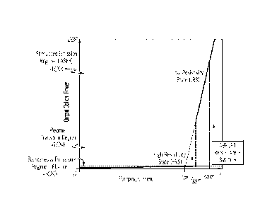
[0064] FIG. 3 is a graph of output optical power versus pumping current of a
classical laser, according to the prior art
which corresponds to the FIG. 1 described above. Shown, adjacent to FIG. 3, is
FIG. 4 which is a graph of output
CA 03166664 2022- 7- 30
WO 2021/186257
PCT/1B2021/050660
optical power versus pumping current of an augmented-laser using a BRS,
according to one embodiment of the
claimed invention. Notice in FIG. 4 that the slope of the curve is almost flat
in the spontaneous emission region 402 up
to the BRS threshold current (IINAT). as compared with the slope of the curve
in the spontaneous emission region 302 of
FIG. 3. This corresponds to the OFF-state of the augmented-Laser where the BRS
in the insulating High Resistance
State (i.e. HRS). In the OFF-state the effective voltage across the laser is
reduced by the potential drop across BRS
due to the large insulator resistance. This reduces the effective pumping
current reaching the active medium of the
LASER, thus reducing the effective Spontaneous Emission below lasing threshold
(It). This mechanism leads to a
much smaller spontaneous emission region 402 as compared with the classic
laser in FIG. 3. As shown the present
invention significantly decreases or eliminates the spontaneous emission
region 402. An optimal or suitable design
augmented-laser design requires to have the Insulator-to-Metal Transition
threshold current (IINAT) of the BRS greater
than the lasing threshold current of the Laser (10. Once the pumping current
reaches the INF value, the BRS abruptly
switches to a Low Resistance State (i.e. LRS) abruptly increasing the
effective pumping current reaching the active
medium above the lasing threshold (10. The augmented-Laser abruptly switches
from a residual spontaneous
emission regime (402) to a stimulated emission regime (406). The Regime
Transition Region (404) with no Output
Optical Power (00P) originates from the abrupt resistance switch of the BRS
and is a region where the laser does not
effectively operate. Similarly, when the pumping current is reduced back to
the I MIT value, the BRS abruptly switches
back to a High Resistance State (i.e. HRS) abruptly decreasing the effective
pumping current reaching the active
medium below the lasing threshold (10. The augmented-Laser abruptly switches
back from the stimulated emission
regime (406) to the residual spontaneous emission regime (402) while
transitioning through the Regime Transition
Region (404).The operating principal is further explained with reference to
FIG. 5A and FIG. 5B.
[0065] FIG. 5A and FIG. 5B are a schematic illustration of an augmented laser
device composed of a BRS electrically
integrated in series with a laser-diode, switching reversibly between OFF-
state and ON-state. In the OFF state in FIG.
5A, when the BRS is in the insulating High Resistance State (HRS), the
effective voltage across the Laser (VLAsER) is
reduced by the potential drop across the BRS due to the large insulator
resistance such that VLAsER = VBA - VBRS.
potential drop across BRS due to the large insulator resistance. This reduces
the effective pumping current reaching
the active medium of the LASER, thus significantly decreasing or eliminating
the spontaneous emission below lasing
threshold (It).
[0066] Referring to FIG. 5B, the ON state is when the BRS is in the metallic
Low Resistance State (LRS), the
effective gate voltage of the LASER is VLAB ER VBA since the potential drop
across the BRS becomes negligible as
the metallic state has multiple orders of magnitude lower resistance. As a
result, the ON-state pumping current loss is
negligible. The reversible resistance switch from HRS to LRS can be
electrically triggered for both positive and
negative voltage polarities.
11
CA 03166664 2022- 7- 30
WO 2021/186257
PCT/1B2021/050660
Various Configurations of Laser Currents with BRS
[0067] FIG. 6 is a series of graphs of output optical power versus pumping
current for various configurations of an
augmented laser with bi-stable resistive system, according to one embodiment
of the present invention. More
specifically, FIG. 6 illustrates four configurations of: i) Optimal
Configuration; ii) Suitable Configuration; iii) Sub-Optimal
Configuration; and iv) Not-Suitable Configuration, as follows:
[0068] i) Optimal Configuration in which;
= switching currents of the BRS are optimized relative to the threshold
voltage of the laser:
= spontaneous emission region is inhibited for all pumping current;
= regime transition region is minimized;
= stimulated emission region is maximized and accessible close to lasing
threshold; and
= In this case !MIT = 6 < limT, where 6 is the laser threshold current for
lasing, IINAT is insulator-to-metal current
and I Nut is metal to insulator current.
[0069] ii) Suitable Configuration in which:
= spontaneous emission region is inhibited for all pumping current;
= regime transition region is larger;
= stimulated emission region is not accessible very close to lasing
threshold;
= need more energy to switch BRS compared to optimal case; and
= In this case Itn < 'MIT < IIMT=
[0070] iii) Sub-Optimal Configuration in which:
= spontaneous emission region accessible is reduced compared to
conventional lasers;
= stimulated emission region regime is not fully inhibited when turning off
the laser: portion is accessible for
pumping currents close and below lasing threshold; and
= partially leveraging benefits of the BRS integration; and
= In this case I miT < Ith < IIMT=
[0071] iv) Not-Suitable Configuration in which
= spontaneous emission region accessible is not significantly reduced
compared to conventional laser;
= Does not leverage benefits of the BRS integration; and
= In this case I m IT < I IMT < Ith=
12
CA 03166664 2022- 7- 30
WO 2021/186257
PCT/1B2021/050660
[0072] FIG. 7 is a series of graphs of output optical power versus pumping
current for various configurations of an
augmented laser with bi-stable resistive system with small or non-existent
hysteresis as compared to the hysteresis in
FIG. 6, according to one embodiment of the present invention. More
specifically, FIG. 7 illustrates three configurations
of: i) Optimal Configuration; ii) Suitable Configuration; and iii) Not-
Suitable Configuration, as follows:
[0073] i) Optimal Configuration in which:
= switching currents of the BRS are optimized relative to the threshold
voltage of the laser;
= spontaneous emission region is inhibited for all pumping current;
= regime transition region is minimized;
= stimulated emission region is maximized and accessible close to lasing
threshold; and
= iMT Imrr = Ith.
[0074] ii) Optimal Configuration in which:
= spontaneous emission region is inhibited for all pumping current;
= regime transition region is larger;
= stimulated emission region is not accessible very close to lasing
threshold;
= Need more energy to switch BRS; and
= In this case It < lIMT Imir.
[0075] iii) Not-Suitable Configuration in which:
= spontaneous emission region accessible is not significantly reduced
compared to conventional lasers;
= does not leverage benefits of the BRS integration; and
= In this case IINAT 11iT < Ith=
Embodiment 1: Vertical Wave Guide Semiconductor Device with BRS with Buried
Bottom Contact
[0076] FIG. 8 is a side view illustrating an initial stage in formation of a
vertical cavity surface emitting laser (VCSEL)
semiconductor device using a bi-stable resistive system (BRS) with a buried
bottom contact, according to one
embodiment of the present invention. In this example a GaAs based VCSEL with
an emission at approximately A
¨980nm is given, however other architectures operating at different
wavelengths are possible.
[0077] Referring to FIG. 8 a VCSEL device is shown, which includes an n-type
GaAs (n-GaAs) substrate 802, and a
layer structure formed thereon by an epitaxial growth process, such as
molecular beam epitaxy (MBE) and/or metal
organic chemical vapor deposition (MOCVD). The layer structure includes
consecutively, as viewed from the GaAs
substrate 802, an n-type lower Distributed Bragg Reflector (DBR) layer or
waveguide layer 804, an active layer or
active medium layer 806 that may include multiple quantum wells, and a p-type
upper DBR layer 810. The p-type
13
CA 03166664 2022- 7- 30
WO 2021/186257
PCT/1B2021/050660
upper DBR 810 includes an oxidation layer 808. For simplicity other optional
layers such as cladding layers between
the active medium 806 and DBR layers 804 and 808 are not shown. The active
medium 806 emits light by
recombination of positive holes and electrons injected from the p-side
electrode (shown) and the n-side electrode (not
shown), respectively.
[0078] The n-type DBR layer 804 as well as the p-type DBR layer 810 includes a
plurality of layer pairs each
including an AlxiiGai_xii as a high-reflectivity layer and an Aix12Ga1_x12 as
low-reflectivity layer where, for example,
x11<1, 0<x121, x11 <x12, x11<x13<x12. The pair of DBR layers 804 and 810
allows the laser generated in the
active layer 806 (3-10 x (I nGaAs/GaAsP) to lase between the DBR layers 804
and 810 and pass through the upper
DBR layer 810 as a laser beam having a desired output power. The upper DBR
layer 810 has a top surface 812 as
shown. The n-type DBR layer 804 may include dopants for GaAs: Substituting As:
Te, S and substituting Ga: Sn, Si,
Ge, where m x (n-GaAs/n-AlAs). The p-type DBR layer 810 may include dopants p-
type dopants for GaAs: substituting
As: Si, Ge and substituting Ga: Zn, Cn and n x (p-GaAs/p-AlAs). Typically, m >
n so that the bottom DBR layer 804
reflectivity close to 100% while top DBR layer 810 has reflectivity less than
100%.
[0079] FIG. 9A is a top perspective view and FIG. 9B is a corresponding cross-
sectional view taken along line X-X'
illustrating a later stage in forming the vertical cavity surface emitting
laser semiconductor device of FIG. 8 with a bi-
stable resistive system integrated on buried bottom contact, according to one
embodiment of the present invention.
[0080] In FIG. 9B, a combination of lithography, anistropic etch,
organic planarization layers (OPL) not shown, is
used to selectively etch the p-type DBR layer 810, the active medium layer
806, the oxidation layer 808, and the n-type
DBR 804 to form a mesa type structure 920 as shown.
[0081] A selective oxidation process is used to form an aperture 922 by
formation of oxide 924 in the oxidation layer
808 as shown. A dielectric layer 950, such as silicon boron carbon nitride
(SiBCN), is conformally deposited over the
top surface and sides of the mesa type structure 920 and over the n-type DBR
804. An OPL (not shown), lithography
patterning and anisotropic etch is used to form bottom contact layer wells
960.
[0082] The OPL (not shown) is removed with using an ash process. A conformal
multi-layer BRS 952 is deposited
followed by lithography and dielectric etch back to form the structure as
shown over the dielectric layer 952 and contact
layer wells 960. In this example the BRS is a threshold switching selector
(TSS), such as ex: Ag/Hf02, Cu/Hf02,
Ag/Ti02. It is important to note that although the integration of a multi-
layer TSS is described an insulator-to-metal
transition (I MT) material or other bi-stable resistive system could be
implemented instead.
[0083] A bottom contact layer 954, such as Ti/Au, is formed on top of
veritical and horizontal portions of the BRS
layer 952 including within the contact layer wells 960 using metal deposition
techniques. Next, a selective recess of the
bottom metal contact layer is performed follow by TSS chamfering using the
bottom metal contact layer formed.
14
CA 03166664 2022- 7- 30
WO 2021/186257
PCT/1B2021/050660
[0084] An upper metal contact layer 926 is formed over the top horizontal
portion of the p-type top DBR layer 810
using using sequential metal deposition, lithography patterning and metal etch
techniques. Using conformal dielectric
deposition a SIN layer is formed 956 on the side walls of the mesa-type
structure 920 and over the bottom contact layer
954. A portion of the bottom contact layer furthest from the mesa-type
structure 920 is exposed after the dielectric
layer 950 is formed as shown. Lithography patterning using OPL (not shown) and
selective dielectric etch back as
shown are used to form the structure.
[0085] A top contact layer 958 is formed over upper contact layer 926 using
sequential metal deposition, lithography
patterning and metal etch techniques. A portion of the bottom contact layer
954 and dielectric layer 950 furthest from
the mesa-type structure 920 is exposed after the dielectric layer 950 is
formed as shown. The top contact layer 958 is
electrically isolated from bottom contact layer 954. A quantization axis 980
is shown parallel to an optical cavity
defined by mesa-type structure 920.
Embodiment 2: Vertical VVaveguide Semiconductor Device with BRS with Top
Contact
[0086] FIG. 10 is a side view of illustrating a vertical cavity surface
emitting laser semiconductor device using a bi-
stable resistive system integrated on a top contact, according to another
embodiment of the present invention. The
process flow for FIG. 8 through FIG. 9A is modified so that the BRS layer 952
is no longer formed.
[0087] In this embodiment prior to formation of the top contact layer
958 and the upper contact layer 926, a BRS
layer 982 is formed using sequential metal deposition, lithography patterning
and etch techniques to form the structure
as shown. The BRS layer 982 is formed over the top horizontal portion of the p-
type top DBR layer 810. In this
example the BRS is a threshold switching selector (TSS), such as ex: Ag/Hf02,
Cu/Hf02, Ag/Ti02. It is important to
note that although the integration of a multi-layer TSS is described an
insulator-to-metal transition (IMT) material or
other bi-stable resistive system could be implemented instead. A quantization
axis 1080 is shown parallel to an optical
cavity defined by mesa-type structure 920.
Embodiment 3: Vertical Wave Guide Semiconductor Device with BRS with Bottom
Contact
[0088] FIG. 11 is a side view illustrating a vertical cavity surface emitting
laser semiconductor device with a bi-stable
resistive system integrated on a back-side contact, according to another
embodiment of the present invention. The
process flow for FIG. 8 through FIG. 9A is modified so that the BRS layer 952
and well 960 are no longer formed.
[0089] In this embodiment the BRS layer 992 is deposited horizontally
on the backside of the substrate 802 followed
by horizontal disposition of a bottom metal contact layer 994, such as Ti/Au
as shown. In this example the BRS is a
threshold switching selector (TSS), such as ex: Ag/Hf02, Cu/Hf02, Ag/Ti02. It
is important to note that although the
CA 03166664 2022- 7- 30
WO 2021/186257
PCT/1B2021/050660
integration of a multi-layer TSS is described an insulator-to-metal transition
(IMT) material or other bi-stable resistive
system could be implemented instead. A quantization axis 1180 is shown
perpendicular to aperture 922.
Flow Diagram of Vertical Wave Guide Semiconductor Device with BRS integrated
on Either a Buried Bottom Contact or
a Top Contact or Back-Side Contact
[0090] FIG. 12 is a flow diagram illustrating one example of a process for
forming a vertical cavity surface emitting
laser semiconductor device with a bi-stable resistive system according to one
embodiment of the present invention. It
should be noted that each of the steps shown has been discussed in greater
detail with respect to FIGs. 8 to 11 above.
The process begins in step 1202 and immediately proceeds to step 1204. In step
1204 a vertical wave guide, such as
vertical-cavity surface-emitting laser (VCSEL), is formed. The vertical wave
guide includes a first wave guide layer
804, with a first doping type disposed over a semiconductor substrate 802, an
active medium layer 806 disposed over
the first wave guide layer 804, and a second wave guide layer 810 with a
second doping type and an oxidation layer
808 disposed over the active medium layer 806. In one example the active
medium layer 806 includes multiple
quantum wells. The process continues to step 1206.
[0091] In step 1206, the first wave guide layer, the active medium layer 806
and the second wave guide layer 810 are
selectively etched to form a mesa type structure 920 with a top surface 812
and a side wall as shown in FIGs. 9B, 10
and 11. The process continues to step 1208.
[0092] In step 1208 is an optional step in which an aperture 922 is
formed in oxidation layer 806 of the second wave
guide layer 810 using a wet oxidation process. The process continues down one
of the three paths denoted by the
dashed line to form either i) buried bottom contact (steps 1210 thru 1216) or
ii) top contact (steps 1218 thru 1224) or iii)
back-side contact (steps 1226 thru 1230).
[0093] In the case of the buried bottom contact, the process continues to step
1210. In step 1210 wells 960 are
etched in the first wave guide layer 804 around the mesa structure 920. The
process continues to step 1212. In step
1212 the bi-stable resistive system 952 is deposited. The process continues to
step 1214. In step 1214 the BRS is
selectively remove from over the top surface 812 of the second wave guide 810
and a portion of the side wall closest to
the top surface 852 of the mesa type structure 920 is removed. The top contact
layer 958 is formed in step 1216. The
processes for forming the bottom contact layer 954, dielectric layer 950,
upper contact layer 926, and the top contact
layer 958 are describe above.
[0094] In the case of the top contact, the process continues to step 1218.
First, the bottom contact layer 954 is
formed in step 1218. Next in step 1220, the bi-stable resistive system is
deposited. The process continues to step
1222. In step 1222 the top contact 958 is formed. The process continues to
step 1224. In step 1224, the bi-stable
resistive system 982 is removed leaving a portion over the top surface the
mesa type structure 920 with an opening
16
CA 03166664 2022- 7- 30
WO 2021/186257
PCT/1B2021/050660
over the optional aperture 922. Processes for forming, upper contact layer
926, and the top contact layer 958 are
described above.
[0095] In the case of the back-side contact, the process continues to step
1226. The bottom contact layer 954 is
formed in step 1226. Next in step 1228, the bi-stable resistive system 992 is
deposited over the bottom surface of the
substrate 802. The process continues to step 1230. In step 1230 a metal
contact layer 994 is formed over the BRS.
Embodiment 4: Fabrication of Edge Emitting Laser-Diode Semiconductor Device
with a BRS integrated on a Top
Contact
[0096] FIG. 13A and 13B are schematic cross-sectional views illustrating an
initial stage in formation of an edge
emitting semiconductor laser or diode device with an integrated bi-stable
resistive system, according to one
embodiment of the present invention.
[0097] Turning to FIG. 130, the laser diode is constructed on a substrate 1302
of n-type GaAs carrying thereon a
layer 1304 of n-type, such as GaAsP having a composition represented as
GaAsyP1¨y, wherein the layer 1302 is
formed by a molecular beam epitaxy (MBE) and/or a metal organic chemical vapor
deposition (MOCVD) process. The
growth process of the layer 1304 is well established a smooth surface is
realized by optimizing the composition
gradient.
[0098] Next, a n-type cladding layer 1304, such as n-type AlGalnAsP, a first
wave guide layer 1306, an undoped
active or active medium with multiple quantum wells layer 1308, such as
InGaAsP, a second wave guide layer 1310, a
p-type cladding layer 1312, such as p-type AlGalnAsP, and a cap layer 1314 of
p-type GaAs formed by an epitaxial
process.
[0099] FIG. 14A and 14B are schematic cross-sectional views illustrating a
later stage in forming the edge emitting
semiconductor laser or diode device with a bi-stable resistive system
integrated on a top contact 1420, according to
one embodiment of the present invention.
[0100] The p-type cladding layer 1312 and the cap layer 1314 are patterned
using lithography techniques and etched
to form a mesa type structure 1420 as shown. Next dielectric isolation layer
is formed to define the top contact region
using sequential Oxide deposition, planarization, lithography patterning and
etch techniques.
[0101] An oxide layer 1430 is formed by a blanket oxide deposition on top of
the p-type cladding layer 1312 including
the top and sides of the mesa-type structure 1420. Next oxide planarization is
used. A combination of organic
planarization layers (OPL), not shown, followed by lithography patterning and
oxide etch are performed. Next the OPL
is removed using an ash process. The removal of cap layer 1314 and selective
etch of top P-type cladding layer 1312.
17
CA 03166664 2022- 7- 30
WO 2021/186257
PCT/1B2021/050660
[0102] Next a bi-stable resistive system (BRS) layer 1432 is formed over the
oxide layer 1430 and the top of the
mesa-type structure 1420 as shown. In this example the BRS 1432 is a threshold
switching selector (TSS), such as
ex: Ag/Hf02, Cu/Hf02, Ag/Ti02. It is important to note that although the
integration of a multi-layer TSS is described
an insulator-to-metal transition (I MT) material or other bi-stable resistive
system could be implemented instead.
[0103] Finally, the top contact layer 1434 is formed over the BRS layer 1432.
Next a back-side contact layer 1436,
such as Ti/Au is deposited on the bottom horizontal surface of the substrate
1302 as shown.
Embodiment 5: Fabrication of Edge Emitting Laser-Diode Semiconductor Device
with a BRS integrated on a Back-side
Contact
[0104] FIG. 15 is a schematic cross-sectional view illustrating a later stage
in forming the edge emitting
semiconductor laser or diode device with a bi-stable resistive system
integrated on a back-side contact, according to
one embodiment of the present invention.
[0105] The process flow for FIGs. 13A-13B through FIGs. 14A-14B is modified so
that the BRS layer is no longer
integrated over the top contact region 1420 and top oxide layer 1430.
[0106] In this embodiment prior to forming a bottom contact layer 1436, a BRS
layer 1536 is deposited on the back
side of the doped-substrate 1302 followed by disposition of a back-side metal
contact layer 1538, such as Ti/Au as
shown.
Embodiment 6: BRS Integration in the Laser active medium within the Optical-
Cavity
[0107] FIG. 16 is a schematic side view illustrating a semiconductor laser
device with a bi-stable resistive system
integrated within the active medium of the laser, according to one embodiment
of the present invention. Illustrated is a
first Distributed Bragg Reflector (DBR) or Waveguide 1602, an active layer or
active medium 1604. The active medium
in one example includes multiple quantum wells formed by a series of barriers
1614 and quantum wells 1616 as known
in the art. Also shown is a second DBR 1608. A bi-stable resistive system
(BRS) layer 1614 is formed. A stationary
electromagnetic field 1620 is depicted. The BRS layer 1614 is deposited in-
situ during the epitaxy process in a node
1622 of the stationary electromagnetic field 1620 oscillating inside the
optical cavity to minimize potential light
absorption. The BRS layer may also act as a barrier. The maximum amplitude
1624 of the stationary electromagnetic
field 1620 is selected to maximize interactions with the quantum wells. Note
this design works for both vertical cavity
and side emitting semiconductor laser devices.
[0108] FIG. 17 is schematic cross-sectional view illustrating the formation of
a vertical cavity surface emitting laser
semiconductor device with a bi-stable resistive system integrated within the
active medium of the device, according to
18
CA 03166664 2022- 7- 30
WO 2021/186257
PCT/1B2021/050660
one embodiment of the present invention. The process flow for FIG. 8 through
FIG. 9A is modified so that a BRS layer
1752 is deposited as shown in FIG. 17 within the optical cavity. A
quantization axis 980 is shown parallel to an optical
cavity defined by mesa-type structure 920.
Embodiment 7: BRS Integration in one of the waveguide constituting the Laser
Optical-Cavity
[0109] FIG. 18 is a schematic side view illustrating a semiconductor laser
device with a bi-stable resistive system
integrated within the waveguide of the laser optical cavity, according to one
embodiment of the present invention.
[0110] Illustrated is a first Distributed Bragg Reflector (DBR) or Waveguide
1602, an active layer or active medium
1604. The active medium in one example includes multiple quantum wells formed
by a series of barriers 1614 and
quantum wells 1616 as known in the art. Also shown is a second DBR 1608. A bi-
stable resistive system (BRS) layer
1814 is created within the wave guide 1602 as shown. A stationary
electromagnetic field 1620 is depicted. The BRS
layer 1614 is deposited in-situ during the epitaxy process at a node 1624 of
the stationary electromagnetic field 1620
oscillating inside the optical cavity to minimize potential light absorption.
The maximum amplitude 1624 of the
stationary electromagnetic field 1620 is selected to maximize interactions
with the quantum wells. Note this design
works for both vertical cavity and side emitting semiconductor laser devices.
The BRS may be integrated in any of the
either one of the waveguides 1602 or 1608.
[0111] FIG. 19 is schematic cross-sectional view illustrating the
formation of a vertical cavity surface emitting laser
semiconductor device with a bi-stable resistive system integrated within the
waveguide of the laser optical cavity,
according to one embodiment of the present invention. The process flow for
FIG. 8 through FIG. 9A is modified.
Instead of a BRS layer 1814 formed as shown in FIG. 18, in this example a BRS
layer 1952 is formed within the optical
cavity. One example of epitaxy-compatible threshold-switching selector is
taught by K. Fu et al., "Threshold Switching
and Memory Behaviors of Epitaxially Regrown GaN-on-GaN Vertical p-n Diodes
With High Temperature Stability," in
IEEE Electron Device Letters, vol. 40, no. 3, pp. 375-378, March 2019. A
quantization axis 1980 is shown parallel to
an optical cavity defined by mesa-type structure 920.
Flow Diagram of Integration Inside Laser Optical-Cavity in Active Component or
Waveguide
[0112] FIG. 20 is a flow diagram illustrating one example of a process for
forming a laser semiconductor device with
a bi-stable resistive system inside the active medium or waveguide of the
laser according to one embodiment of the
present invention. It should be noted that each of the steps shown in FIG. 20
has been discussed in greater detail with
respect to FIGs. 13 to 19 above. The process begins in step 2002 and
immediately proceeds to step 2004. In step
2004 a vertical wave guide, such as vertical-cavity surface-emitting laser
(VCSEL), is formed. The vertical wave guide
includes a first wave guide layer 804, with a first doping type disposed over
a semiconductor substrate 802, an active
medium layer 806 disposed over the first wave guide layer 804, and a second
wave guide layer 810 with a second
19
CA 03166664 2022- 7- 30
WO 2021/186257
PCT/1B2021/050660
doping type and an oxidation layer 808 disposed over the active medium layer
806. In one example a bi-stable
resistive system layer 1614 is formed within the active medium. In another
example, a bi-stable resistive system layer
1814 is formed within the second wave guide layer 810. The active medium layer
806 may include multiple quantum
wells. The process continues to step 2006.
[0113] In step 2006, the first wave guide layer 804, the active medium layer
806 and the second wave guide layer
810 to form a mesa type structure 920 with a top surface and a side wall as
shown above. The process continues to
step 2008.
[0114] In step 2008 is an optional step in which an aperture 922 is formed in
the oxidation layer of the second wave
guide layer 810. The process completes in step 2010.
CA 03166664 2022- 7- 30