Note: Descriptions are shown in the official language in which they were submitted.
CA 03167892 2022-07-14
WO 2021/146477 PCT/US2021/013509
WAVEGUIDE EXCITATION UNIFORMITY
RELATED APPLICATION
[0001] This application claims the benefit under 35 U.S.C. 119(e) of U.S.
Provisional
Application Ser. No. 62/960,954, filed January 14, 2020 and titled "WAVEGUIDE
EXCITATION UNIFORMITY," which is hereby incorporated herein by reference in
its entirety.
FIELD OF THE APPLICATION
[0002] The present application is directed generally to devices, methods, and
techniques for
coupling optical energy into an integrated device and distributing optical
energy to multiple
regions of the device. The integrated device may be used for performing
parallel, quantitative
analysis of biological and/or chemical samples, including for nucleic acid
sequencing and protein
sequencing.
BACKGROUND
[0003] Instruments that are capable of massively-parallel analyses of
biological or chemical
samples are typically limited to laboratory settings because of several
factors that can include
their large size, lack of portability, requirement of a skilled technician to
operate the instrument,
power demands, need for a controlled operating environment, and cost.
Moreover, some
analysis of biological or chemical samples is performed in bulk such that a
large amount of a
particular type of sample is necessary for detection and quantitation.
[0004] Analysis of biological or chemical samples may involve tagging samples
with
luminescent markers that emit light of a particular wavelength, illuminating
with a light source
the tagged samples, and detecting the luminescent light with a photodetector.
Such techniques
conventionally involve expensive laser light sources and systems to illuminate
the tagged
samples as well as complex detection optics and electronics to collect the
luminescence from the
tagged samples.
SUMMARY
[0005] Some embodiments are directed to a system including an array of
reaction chambers and
a waveguide that delivers excitation light to at least a portion of the
reaction chambers, wherein a
vertical extent of an optical mode of the waveguide is modulated to adjust
confinement of light
within the waveguide.
[0006] In some embodiments, the vertical extent of the optical mode is
modulated by changing a
thickness of a waveguide core layer along the length of the waveguide.
1
CA 03167892 2022-07-14
WO 2021/146477 PCT/US2021/013509
[0007] In some embodiments, the vertical extent of the optical mode is
modulated by changing a
refractive index of a waveguide core or cladding material along the length of
the waveguide.
[0008] In some embodiments, the thickness of the waveguide core layer along
the length of the
waveguide is changed by transferring a topography of a photoresist layer.
[0009] In some embodiments, the system comprises a plurality of waveguides
having uniform
widths; and a plurality of dummy structures having tapered widths, wherein the
plurality of
waveguides and the plurality of dummy structures are disposed alternatively.
[0010] In some embodiments, the plurality of waveguides and the plurality of
dummy structures
are in a waveguide core layer.
[0011] Some embodiments are directed to a system including an array of
reaction chambers and
a waveguide that delivers excitation light to at least a portion of the
reaction chambers, wherein a
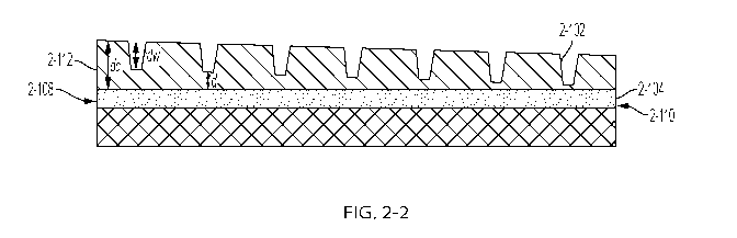
distance between the waveguide and the reaction chambers is modulated to
compensate for
waveguide losses.
[0012] In some embodiments, a thickness of a cladding layer of the waveguide
is controlled to
modulate the distance between the waveguide and the reaction chambers.
[0013] In some embodiments, the system comprises a plurality of waveguides
having uniform
widths; and a plurality of dummy structures having tapered widths, wherein the
plurality of
waveguides and the plurality of dummy structures are disposed alternatively.
[0014] In some embodiments, the system comprises a plurality of waveguides
having tapered
widths; and a plurality of dummy structures having tapered widths, wherein the
plurality of
waveguides and the plurality of dummy structures are disposed alternatively.
[0015] In some embodiments, the system comprises a plurality of waveguides
having tapered
widths in a first direction; and a plurality of dummy structures having
tapered widths in a second
direction opposite to the first direction, wherein the plurality of waveguides
and the plurality of
dummy structures are disposed alternatively.
[0016] Some embodiments are directed to a method comprising providing a
waveguide to
deliver excitation light to an array of reaction chambers and modulating a
vertical extent of an
optical mode of the waveguide to adjust confinement of light within the
waveguide.
[0017] In some embodiments, the modulating includes changing a thickness of a
waveguide core
layer along the length of the waveguide.
[0018] In some embodiments, the modulating includes changing a refractive
index of a
waveguide core or cladding material.
[0019] Some embodiments are directed to a method comprising providing a
waveguide to
deliver excitation light to an array of reaction chambers and modulating a
distance between the
waveguide and reaction chambers.
2
CA 03167892 2022-07-14
WO 2021/146477 PCT/US2021/013509
[0020] In some embodiments, the modulating includes controlling a thickness of
a cladding layer
of the waveguide.
[0021] In some embodiments, controlling the thickness of the cladding layer of
the waveguide
includes providing the cladding layer with a tapered thickness by planarizing
a material for the
cladding layer on a modulated waveguide pattern.
[0022] In some embodiments, controlling the thickness of the cladding layer of
the waveguide
includes providing the cladding layer with a tapered thickness by depositing a
material for the
cladding layer on a modulated waveguide pattern.
[0023] In some embodiments, controlling the thickness of the cladding layer of
the waveguide
includes providing the cladding layer with a tapered thickness by transferring
a topography of a
photoresist layer to the cladding layer.
[0024] Some embodiments are directed to a method comprising forming an array
of reaction
chambers; forming a waveguide to deliver excitation light to the reaction
chambers; and
modulating the waveguide to deliver as close to an equal amount of excitation
light to each
reaction chamber.
[0025] In some embodiments, the modulating includes modulating a vertical
extent of the optical
mode of the waveguide.
[0026] In some embodiments, the modulating includes modulating a thickness
along its length of
the waveguide.
[0027] In some embodiments, the modulating includes modulating a distance
along its length of
the waveguide from each reaction chamber.
[0028] Some embodiments are directed to a method comprising exciting with
excitation light
delivered through a waveguide a sample within each of a plurality of reaction
chambers, wherein
the waveguide is modulated such that a substantially same amount of light is
delivered to each
reaction chamber.
[0029] The foregoing summary is provided by way of illustration and is not
intended to be
limiting.
BRIEF DESCRIPTION OF THE DRAWINGS
[0030] Various aspects and embodiments of the application will be described
with reference to
the following figures. It should be appreciated that the figures are not
necessarily drawn to scale.
Items appearing in multiple figures are indicated by the same reference number
in all the figures
in which they appear.
[0031] FIG. 1-1 is a cross-sectional schematic of an integrated device,
according to some
embodiments.
3
CA 03167892 2022-07-14
WO 2021/146477 PCT/US2021/013509
[0032] FIG. 1-2 is a planar schematic of an integrated device, according to
some embodiments.
[0033] FIG. 2-1 is a planar schematic of a waveguide array, showing sample
wells, waveguides,
and dummy structures, according to some embodiments.
[0034] FIG. 2-2 is a cross-sectional view of the waveguide array of FIG. 2-1
along a line marked
"2-2", illustrating a waveguide cladding layer with a modulated thickness
along the length of a
waveguide, according to some embodiments.
[0035] FIGs. 2-3A ¨ 2-3C are cross-sectional views of the waveguide array of
FIG. 2-1 along a
line marked "2-3", illustrating a first method for fabricating the waveguide
array, according to
some embodiments.
[0036] FIGs. 2-4A ¨ 2-4C are cross-sectional views of the waveguide array of
FIG. 2-1 along a
line marked "2-4", illustrating the first method for fabricating the waveguide
array, according to
some embodiments.
[0037] FIGs. 2-5A ¨ 2-5B are cross-sectional views of the waveguide array of
FIG. 2-1 along the
line marked "2-3", illustrating a second method for fabricating the waveguide
array, according to
some embodiments.
[0038] FIGs. 2-6A ¨ 2-6B are cross-sectional views of the waveguide array of
FIG. 2-1 along the
line marked "2-4", illustrating the second method for fabricating the
waveguide array, according
to some embodiments.
[0039] FIG. 2-7A is an enlarged view of a region marked "2-7" in FIG. 2-3C,
according to some
embodiments.
[0040] FIG. 2-7B is a schematic illustrating field intensity of an optical
mode within and near
the waveguide of FIG. 2-7A, according to some embodiments.
[0041] FIG. 2-8 is a planar schematic of a waveguide array with an alternative
layout for sample
wells, according to some embodiments.
[0042] FIG. 3-1 is a planar schematic of a waveguide array, showing sample
wells, waveguides,
and dummy structures, according to some embodiments.
[0043] FIG. 4-1 is a planar schematic of a waveguide array, showing sample
wells, waveguides,
and dummy structures, according to some embodiments.
[0044] FIGs. 4-2A ¨ 4-2B are cross-sectional views of the waveguide array of
FIG. 4-1 along the
line marked "4-2", illustrating a method for fabricating the waveguide array,
according to some
embodiments.
[0045] FIG. 5-1A is a block diagram of an integrated device and an instrument,
according to
some embodiments.
[0046] FIG. 5-1B is a schematic of an apparatus including an integrated
device, according to
some embodiments.
4
CA 03167892 2022-07-14
WO 2021/146477 PCT/US2021/013509
[0047] FIG. 5-2 is a schematic of a pixel having a sample well, optical
waveguide, and time-
binning photodetector, according to some embodiments.
[0048] FIG. 5-3 is a schematic of an exemplary biological reaction that may
occur within a
sample well, according to some embodiments.
[0049] FIG. 5-4 is a plot of emission probability curves for two different
fluorophores having
different decay characteristics.
[0050] FIG. 5-5 is a plot of time-binning detection of fluorescent emission,
according to some
embodiments.
[0051] FIG. 5-6 is an exemplary time-binning photodetector, according to some
embodiments.
[0052] FIG. 5-7A is a schematic illustrating pulsed excitation and time-binned
detection of
fluorescent emission from a sample, according to some embodiments.
[0053] FIG. 5-7B is a histogram of accumulated fluorescent photon counts in
various time bins
after repeated pulsed excitation of a sample, according to some embodiments.
[0054] FIGs. 5-8A ¨ 5-8D are different histograms that may correspond to the
four nucleotides
(T, A, C, G) or nucleotide analogs, according to some embodiments.
DETAILED DESCRIPTION
I. Introduction
[0055] Aspects of the present application relate to integrated devices,
instruments and related
systems capable of analyzing samples in parallel, including identification of
single molecules
and nucleic acid sequencing. Such an instrument may be compact, easy to carry,
and easy to
operate, allowing a physician or other provider to readily use the instrument
and transport the
instrument to a desired location where care may be needed. Analysis of a
sample may include
labeling the sample with one or more fluorescent markers, which may be used to
detect the
sample and/or identify single molecules of the sample (e.g., individual
nucleotide identification
as part of nucleic acid sequencing). A fluorescent marker may become excited
in response to
illuminating the fluorescent marker with excitation light (e.g., light having
a characteristic
wavelength that may excite the fluorescent marker to an excited state) and, if
the fluorescent
marker becomes excited, emit emission light (e.g., light having a
characteristic wavelength
emitted by the fluorescent marker by returning to a ground state from an
excited state).
Detection of the emission light may allow for identification of the
fluorescent marker, and thus,
the sample or a molecule of the sample labeled by the fluorescent marker.
According to some
embodiments, the instrument may be capable of massively-parallel sample
analyses and may be
configured to handle tens of thousands of samples or more simultaneously.
CA 03167892 2022-07-14
WO 2021/146477 PCT/US2021/013509
[0056] The inventors have recognized and appreciated that an integrated
device, having sample
wells [also referred to as reaction chambers] configured to receive the sample
and integrated
optics formed on the integrated device, and an instrument configured to
interface with the
integrated device may be used to achieve analysis of this number of samples.
The instrument
may include one or more excitation light sources, and the integrated device
may interface with
the instrument such that the excitation light is delivered to the sample wells
using integrated
optical components (e.g., waveguides, optical couplers, optical splitters)
formed on the integrated
device. The optical components may improve the uniformity of illumination
across the sample
wells of the integrated device and may reduce a large number of external
optical components that
might otherwise be needed. Furthermore, the inventors have recognized and
appreciated that
integrating photodetectors on the integrated device may improve detection
efficiency of
fluorescent emissions from the sample wells and reduce the number of light-
collection
components that might otherwise be needed.
[0057] According to some embodiments, the integrated device has an array of
sample wells,
which allow for multiplexed analysis of multiple samples across the array, and
an optical system
configured to deliver excitation light to the array of sample wells.
Performance of the integrated
device may depend on the ability of the integrated device to deliver
excitation light across the
array of sample wells using the optical system. Additionally, performance of
the integrated
device may relate to the ability of the optical system to deliver excitation
light to individual
sample wells in a substantially uniform manner, such as by delivering a
relatively constant
intensity or electric field strength to individual sample wells. Specifically,
performance related
factors related to the optical system may include optical loss arising from
scattering and/or
absorption by the sample wells, the coupling efficiency of an optical coupler
(e.g., a grating
coupler configured to receive light from an external light source), optical
loss arising from
splitting excitation light among multiple waveguides, and coupling efficiency
of individual
waveguides with multiple sample wells.
[0058] To increase the multiplexing capabilities of the integrated device, it
can be desirable to
increase the number of sample wells in the array to allow for the ability to
analyze more samples
at any particular time while using the integrated device. As the integrated
device is scaled by
increasing the number of sample wells, challenges in performance of the
integrated device may
arise because of one or more of these factors. For example, a row of sample
wells may receive
light by coupling to a waveguide of the optical system such that as light
propagates along the
waveguide, the sample wells in the row receive a portion of the light. Optical
loss may arise
from the individual sample wells scattering and/or absorbing the light, which
may cumulatively
result in the last sample well in the row (e.g., distal from the optical input
end of the waveguide)
6
CA 03167892 2022-07-14
WO 2021/146477 PCT/US2021/013509
receiving a lower intensity or electric field strength than the first sample
well in the row (e.g., the
sample well proximate to the optical input end of the waveguide). Such optical
loss may impact
the signal-to-noise ratio of the measurements conducted by using the
integrated device. As more
sample wells are added to an array, these optical losses may lead to further
reduction in signal-
to-noise ratio, which can impact the quality and reliability of the analysis
conducted.
[0059] Accordingly, aspects of the present application relate to optical
components and
particular arrangements to include in an optical system of the integrated
device that may allow
for improved distribution of light among an array of sample wells. These
optical components
and arrangements may allow for delivering light in a substantially uniform
manner such that
individual sample wells, including sample wells within the same row, receive a
similar intensity
and/or electric field strength. The optical components and arrangements
described herein may
allow for the implementation of integrated devices having a larger number of
sample wells in the
array, as well as a desired performance in analyzing samples across the array.
[0060] Additional considerations as part of scaling up the number of sample
wells in the array
may include fabrication costs and constraints. Accordingly, aspects of the
present application
relate to optical components and systems that take into account fabrication
costs and constraints
(e.g., by reducing the number or complexity of the fabrication steps) while
allowing for the
resulting integrated device to achieve a desired optical performance.
[0061] Some aspects of the present application relate to waveguide
configurations that may
allow for illuminating a large number of sample wells and/or other photonic
elements, in a
substantially uniform manner.
[0062] In particular, some aspects are directed to modulating a vertical
extent of an optical mode
of a waveguide to adjust confinement of light within, and along the length of,
the waveguide.
This modulation may compensate for optical losses. This modulation enables
more uniform
distribution of excitation light to the sample wells, improve excitation
efficiency, and prevent
overpower on regions of the integrated device. The modulation may be
accomplished by
changing a thickness and/or width of the waveguide, changing a refractive
index of the
waveguide and/or a refractive index of the waveguide's cladding material, or
any suitable
combinations of the techniques described herein.
[0063] Other aspects are directed to modulating a distance between a waveguide
and sample
wells to compensate for optical losses. This modulation of the distance may be
carried out by
controlling a thickness of a cladding layer of the waveguide. Accordingly,
aspects of the present
application relate to techniques for controlling the thickness of the cladding
layer of the
waveguide along the length of the waveguide. In some embodiments, the
techniques may
include modulating a waveguide pattern density. In some embodiments, the
techniques may
7
CA 03167892 2022-07-14
WO 2021/146477 PCT/US2021/013509
include modulating the topography of the cladding layer. In some embodiments,
the techniques
may include modulating the lateral positions of the sample wells relative to a
waveguide. In
some embodiments, the techniques may be used alone or in any suitable
combination.
[0064] Additional systems and methods for delivering uniform excitation light
to an array of
sample wells are described in U.S. patent application Ser. No. 16/733,296
titled "OPTICAL
WAVEGUIDES AND COUPLERS FOR DELIVERING LIGHT TO AN ARRAY OF
PHOTONIC ELEMENTS," which is herein incorporated by reference in its entirety.
[0065] While the techniques for an optical system as described in the present
application are
discussed in connection with delivering excitation light to an array of sample
wells, it should be
appreciated that one or more of these techniques may be used, alone or in
combination, in other
contexts that involve distributing light to an array of photonic elements
within an integrated
device. For example, the techniques of the present application may be
implemented in an array
of optical components, such as an array of sensors. In other words, rather
than, or in addition to,
providing techniques to deliver uniform excitation light to an array of sample
wells, techniques
can be employed to address non-uniformities in excitation light delivery
within optical
components used to deliver or receive emission light from excited samples
within the sample
wells. Additionally, it should be appreciated that the techniques described
herein are not limited
to the context of analyzing biological or chemical samples, but rather may be
implemented in
applications where it is desired to distribute light among many photonic
elements in substantially
uniform manner.
[0066] The aspects and embodiments described above, as well as additional
aspects and
embodiments, are described further below. These aspects and/or embodiments may
be used
individually, all together, or in any combination of two or more, as the
application is not limited
in this respect.
II. Integrated Device
[0067] A. Overview
[0068] A cross-sectional schematic of integrated device 1-102 illustrating a
row of pixels 1-112
is shown in FIG. 1-1. Integrated device 1-102 may include coupling region 1-
201, routing
region 1-202, and pixel region 1-203. As discussed herein, an optical system
of the integrated
device may include different types of optical components, which may be located
within regions
1-201, 1-202, and 1-203 of the integrated device. Coupling region 1-201 may
include grating
coupler 1-216, which may be configured to receive excitation light (shown in
the dashed line)
and propagate the excitation light to one or more optical components in
routing region 1-202.
Routing region 1-202 may include an optical routing network configured to
split light among
multiple waveguides 1-220 configured to propagate light to pixel region 1-203.
Pixel region 1-
8
CA 03167892 2022-07-14
WO 2021/146477 PCT/US2021/013509
203 may include a plurality of pixels 1-112 having sample wells 1-108
positioned on a surface at
a location separate from coupling region 1-201, which is where excitation
light (shown as the
dashed arrow) couples to integrated device 1-102. Sample wells 1-108 may be
formed through
metal layer(s) 1-106. One pixel 1-112, illustrated by the dotted rectangle, is
a region of
integrated device 1-102 that includes a sample well 1-108 and photodetector
region having one
or more photodetectors 1-110.
[0069] FIG. 1-1 illustrates the path of excitation (shown in dashed lines) by
coupling a beam of
excitation light to coupling region 1-201 and to sample wells 1-108. The row
of sample wells 1-
108 shown in FIG. 1-1 may be positioned to optically couple with waveguide 1-
220. Excitation
light may illuminate a sample located within a sample well. The sample may
reach an excited
state in response to being illuminated by the excitation light. When a sample
is in an excited
state, the sample may emit emission light, which may be detected by one or
more photodetectors
associated with the sample well. FIG. 1-1 schematically illustrates the path
of emission light
(shown as the solid line) from a sample well 1-108 to photodetector(s) 1-110
of pixel 1-112. The
photodetector(s) 1-110 of pixel 1-112 may be configured and positioned to
detect emission light
from sample well 1-108. Examples of suitable photodetectors are described in
U.S. Pat.
Application 14/821,656 titled "INTEGRATED DEVICE FOR TEMPORAL BINNING OF
RECEIVED PHOTONS," which is incorporated by reference in its entirety.
Additional
examples of suitable photodetectors are described in U.S. Pat. Application No.
15/852,571, titled
"INTEGRATED PHOTODETECTOR WITH DIRECT BINNING PIXEL," which is
incorporated herein by reference in its entirety. For an individual pixel 1-
112, a sample well 1-
108 and its respective photodetector(s) 1-110 may be aligned along a common
axis (along the y-
direction shown in FIG. 1-1). In this manner, the photodetector(s) may overlap
with the sample
well within a pixel 1-112.
[0070] A planar view of integrated device 1-102 illustrating five rows of
pixels is shown in
FIG. 1-2. As shown in FIG. 1-2, sample well 1-108a and sample well 1-108b are
in the same
row and sample well 1-108c and 1-108d are in the same row. Aspects of the
present application
relate to techniques for receiving excitation light incident to coupling
region 1-201 and
propagating excitation light to the array of sample wells 1-108. These
techniques may include
having one or more optical grating couplers positioned in coupling region 1-
201 and waveguide
architecture, positioned in routing region 1-202 and/or pixel region 1-203,
for delivering
excitation light from the coupling region 1-201 to the individual sample wells
1-108.
[0071] B. Waveguide Architecture
[0072] Some embodiments relate to waveguides configured to substantially
uniformly couple
excitation energy generated by an excitation source to individual samples in
sample wells
9
CA 03167892 2022-07-14
WO 2021/146477 PCT/US2021/013509
through, for example, evanescent coupling. In some embodiments, sample wells
may be
disposed in an array having rows and columns, and individual waveguides may be
configured to
deliver excitation energy to sample wells in corresponding rows or columns. In
some
embodiments, the waveguides may be configured to substantially uniformly
provide (e.g., with a
variation in intensity that is less than 50%; in some embodiments, less than
20%; in some
embodiments, less than 10%) excitation energy among the sample wells in a row
or column
and/or in multiple rows or columns. In some embodiments, the number of sample
wells along a
waveguide may be larger than 500, for example, in the range of 500 to 5000.
[0073] The waveguides may be configured to compensate for optical losses.
Optical losses may
cause nonuniform excitation within an array, and/or result in suboptimal
excitation efficiencies,
which may be referred to as the number of measurements enabled by an optical
power. Without
compensation, the power in a waveguide may decrease, for example,
exponentially with respect
to the distance it traverses across a waveguide array. Embodiments of the
waveguides are
configured to improve excitation uniformity and excitation efficiency across
large arrays of
sample wells, and to prevent overpower on regions of an integrated device
comprising large
arrays of sample wells.
[0074] Vertical extents of optical modes of individual waveguides may be
modulated to adjust
confinement of light within, and along the length of, the waveguides. In some
embodiments, the
thicknesses and/or widths of individual waveguides may be modulated along the
lengths of
individual waveguides. In some embodiments, the refractive index of the
waveguides and/or the
refractive index of its cladding material may be modulated.
[0075] In some embodiments, the distances between a waveguide and respective
sample wells
may be modulated to adjust the excitation of sample wells along the waveguide.
In some
embodiments, the distances between a waveguide and respective sample wells may
be modulated
by modulating the thickness of a waveguide cladding layer along the length of
the waveguide. In
some embodiments, the distances between a waveguide and respective sample
wells may be
modulated by modulating the lateral position of the sample wells with respect
to the waveguide
along the length of the waveguide. For example, the sample wells may be
disposed such that,
along the length of a waveguide, sample wells closer in distance to an
excitation source are offset
more from the waveguide than sample wells farther away from the excitation
source. The offset
may be in a direction perpendicular to the direction that the waveguide
extends (for example, as
illustrated in FIG. 2-8). In some embodiments, the techniques described herein
may be used
alone or in any suitable combination.
[0076] In some embodiments, a thickness profile of a cladding layer on top of
an array of
waveguides may be modulated. FIG. 2-1 illustrates a planar schematic of a
waveguide array 2-
CA 03167892 2022-07-14
WO 2021/146477 PCT/US2021/013509
100, according to some embodiments. The waveguide array 2-100 may extend from
an array
beginning end 2-108 to an array ending end 2-110. The array beginning end 2-
108 may be closer
in distance to an excitation source than the array ending end 2-110. The
waveguide array 2-100
may include waveguides 2-104 and dummy structures 2-106 disposed in between
adjacent
waveguides 2-104. Waveguides 2-104 and dummy structures 2-106 may be in a
waveguide core
layer. For example, a waveguide core layer may be deposited on a substrate and
patterned into
waveguides and dummy structures. Sample wells 2-102 may be disposed on top of
the
waveguides 2-104. There may be no sample wells disposed on top of the dummy
structures 2-
106. Such configuration may allow the dimensions (e.g., width) of the dummy
structures 2-106
adapted according to the needs of subsequent fabrication processes, while the
dimensions of the
waveguides 2-104 adapted for modulating vertical extents of optical modes of
the waveguides to
adjust confinement of light within, and along the lengths of, the waveguides.
For example, the
results of some subsequent fabrication processes such as chemical mechanical
polishing (CMP)
and high density plasma chemical vapor deposition (HDP) may depend on the
pattern density of
an underlying layer. The addition of the dummy structures may allow the
modulation of the
pattern density of a photolithography mask designed for the waveguides 2-104
to achieve a
desired pattern density for the subsequent fabrication processes, by
modulating the dimensions of
the dummy structures 2-106 and without changing the dimensions of the
waveguides 2-104 that
are adapted for modulated vertical extents of optical modes.
[0077] The waveguide array 2-100 may have a modulated pattern density. The
pattern density
may be configured to decrease as the distance to the excitation source
increase. In the illustrated
example, the waveguides 2-104 have constant widths along the lengths of the
waveguides, which
may be configured to maintain a steep decay rate of the evanescent field. In
the illustrated
example, the dummy structures 2-106 have tapered widths along the length of
the dummy
structures, which causes, from the array beginning end 2-108 to the array
ending end 2-110, a
decrease of the waveguide pattern density.
[0078] Distances between the waveguides 2-104 and sample wells 2-102 may be
modulated
based, at least in part, on the modulated waveguide pattern density. The
distances between a
waveguide 2-104 and a row of sample wells 2-102 on top of the waveguide may be
configured to
decrease as the waveguide extends away from the excitation source. FIG. 2-2
illustrates a cross-
sectional view of the waveguide array 2-100 along a line marked "2-2" in FIG.
2-1, according to
some embodiments. A cladding layer 2-112 may be formed on top of the waveguide
2-104. A
thickness dc of the cladding layer 2-112 may be modulated along the length of
the waveguide 2-
104. As illustrated, the thickness dc of the cladding layer 2-112 gradually
tapers from the array
beginning end 2-108 to the array ending end 2-110. Sample wells 2-102 may be
formed in the
11
CA 03167892 2022-07-14
WO 2021/146477 PCT/US2021/013509
cladding layer 2-112 by, for example, photolithography and etching. As the
depths dw of the
sample wells 2-102 may be substantially constant for defining the locations of
the sample,
distances between the sample wells 2-102 and the waveguide 2-104 may therefore
decrease
along the length of the waveguide 2-104. The reduced sample-to-waveguide
distance can
compensate for the loss of power in the waveguide as the excitation energy
traverses across the
waveguide and away from the excitation source, and enable a substantially
similar amount of
light to interact with samples in the sample wells along the length of the
waveguide and/or across
different regions of the waveguide array.
[0079] In some embodiments, the waveguide array 2-100 may be fabricated with a
first method
illustrated in FIG. 2-3A ¨ 2-4C. FIGs. 2-3A ¨ 2-3C illustrate cross-sectional
views of the
waveguide array 2-100 along a line near the array beginning end 2-108 and
marked "2-3" in FIG.
2-1, according to some embodiments. FIGs. 2-4A ¨ 2-4C illustrate cross-
sectional views of the
waveguide array 2-100 along a line near the array ending end 2-110 and marked
"2-4" in FIG. 2-
1, according to some embodiments.
[0080] In the fabrication step illustrated in FIG. 2-3A and FIG. 2-4A,
waveguides 2-104 and
dummy structures 2-106 may be fabricated by depositing a layer of waveguide
core material on a
substrate and patterning the layer of waveguide core material by lithography
and etching.
[0081] In the fabrication step illustrated in FIG. 2-3B and FIG. 2-4B, a
cladding layer 2-114 may
be deposited on top of the patterned layer of waveguide core material using a
deposition process
substantially independent of the underlying pattern density, for example,
plasma enhanced
chemical vapor deposition (PECVD). As illustrated, the thickness dd of the
deposited cladding
layer 2-114 may be substantially constant from the array beginning end 2-108
to the array ending
end 2-110.
[0082] In the fabrication step illustrated in FIG. 2-3C and FIG. 2-4C, the
cladding layer 2-112
may be formed by polishing/planarizing the deposited cladding layer 2-114
using, for example, a
chemical mechanical polishing (CMP) process. The CMP process may be configured
such that a
region that has lower waveguide pattern density is polished faster than a
region that has higher
waveguide pattern density. As illustrated, the thickness dl of the cladding
layer 2-112 at the
array beginning end 2-108 is larger than the thickness d2 of the cladding
layer 2-112 at the array
ending end 2-110.
[0083] In some embodiments, the waveguide array 2-100 may be fabricated with a
second
method illustrated in FIGs. 2-5A ¨ 2-6B. FIGs. 2-5A ¨ 2-5B illustrate cross-
sectional views of
the waveguide array 2-100 along the line near the array beginning end 2-108
and marked "2-3"
in FIG. 2-1, according to some embodiments. FIGs. 2-6A ¨ 2-6B illustrate cross-
sectional views
12
CA 03167892 2022-07-14
WO 2021/146477 PCT/US2021/013509
array 2-100 along a line near the array beginning end 2-108 and marked "2-4"
in FIG. 2-1,
according to some embodiments.
[0084] Similar to the fabrication step illustrated in FIG. 2-3A and FIG. 2-4A,
in the fabrication
step illustrated in FIG. 2-5A and FIG. 2-6A, the waveguides 2-104 and dummy
structures 2-106
may be fabricated by depositing a layer of waveguide core material on the
substrate and
patterning the layer of waveguide core material by lithography and etching.
[0085] Different from the fabrication step illustrated in FIG. 2-3B and FIG. 2-
4B, in the
fabrication step illustrated in FIG. 2-5B and FIG. 2-6B, a cladding layer 2-
116 may be deposited
on top of the patterned layer of waveguide core material using a deposition
process dependent on
the underlying pattern density, for example, high density plasma chemical
vapor deposition
(HDP). As illustrated, the thickness ddl of the deposited cladding layer 2-116
at the array
beginning end 2-108 is larger than the thickness dd2 of the deposited cladding
layer 2-116 at the
array ending end 2-110.
[0086] After the fabrication step illustrated in FIG. 2-5B and FIG. 2-6B,
similar to the
fabrication step illustrated in FIG. 2-3C and FIG. 2-4C, the cladding layer 2-
112 may be formed
by polishing/planarizing the deposited cladding layer 2-116 using, for
example, CMP process.
The thickness profile of the deposited cladding layer 2-116 may be maintained
or enhanced when
it is transferred to the cladding layer 2-112 by the polishing/planarizing
process.
[0087] The vertical extent of the optical mode of a waveguide may be modulated
by a tapered
cladding layer (e.g., the cladding layer 2-112 shown in FIG. 2-2). FIG. 2-7A
is an enlarged view
of a region marked "2-7" in FIG. 2-3C, according to some embodiments. FIG. 2-
7B is a
simulated schematic illustrating field intensity of an optical mode within and
near a waveguide
2-104, according to some embodiments. The field intensity of the optical mode
of the
waveguide 2-104 may depend on the width w and thickness t of the waveguide. As
illustrated,
the optical mode has a substantial elliptical shape with the field intensity
decreasing with the
increase of distance to the center of the optical mode. The field intensity
may have another
shape depending on the configuration of the integrated device.
[0088] In FIG. 2-7A, a shape 2-118 is drawn to illustrate an example of the
locations having an
equal field intensity. The field may decay rapidly in a vertical direction
that is parallel to the
thickness of the waveguide. Also, as the waveguide traverses away from the
excitation source,
the power at the center of the waveguide decays in a horizontal direction that
is parallel to the
length of the waveguide and perpendicular to the width w and thickness t of
the waveguide.
Modulating the vertical extent of the optical mode of a waveguide along the
length of the
waveguide may bring sample wells that are farther away from the excitation
source closer to the
13
CA 03167892 2022-07-14
WO 2021/146477 PCT/US2021/013509
waveguide, and therefore enable as close to as possible the same amount of
light to be delivered
to the sample wells along the length of a waveguide and/or across different
regions of an array.
[0089] In some embodiments, the vertical extent of the optical mode may be
modulated by
changing the thickness t of a waveguide along the length of the waveguide. For
example, the
thickness t of a waveguide may be increased as the waveguide extends away from
the excitation
source so as to bring the waveguide closer to sample wells that are farther
away from the
excitation source. In some embodiments, the thickness t of a waveguide may be
modulated by
transferring a topography of a photoresist layer to the waveguide core layer.
The photoresist
layer may be deposited on top of the waveguide core layer and provided with a
desired surface
profile after a grayscale lithography. Then the desired surface profile of the
photoresist layer
may be transferred to the waveguide core layer after a non-selective etch. It
should be
appreciated that the above is provided as an example and any other suitable
fabrication processes
may be used to provide a waveguided with a desired changing thickness along
its length.
[0090] Additionally or alternatively, in some embodiments, the refractive
index of the
waveguides and/or the refractive index of its surrounding cladding material
may be modulated.
For example, ion implantation methods may be used to change the local
composition of the
waveguide core layer and/or cladding layer, which in turn modulates the
refractive index.
[0091] The waveguides may be fabricated from a waveguide core material that is
transparent
(e.g., having a propagation loss that is less than 2 dB/m) at the wavelength
of the excitation
energy. For example, silicon nitride may be used as material for guiding
excitation energy.
Other materials that can be suitable for forming the waveguide core include
silicon carbide and
alloys of silicon nitride and silicon carbide. The waveguide cladding layer
may be fabricated
from a transparent material that provides a desired decay rate with respect to
the waveguide core
material. For example, silicon dioxide may be used as material for a cladding
layer. These
waveguide core and cladding materials may be deposited by methods such as
plasma enhanced
chemical vapor deposition (PECVD), and the optical properties of the materials
may be tuned by
adjusting the deposition parameters.
[0092] In some embodiments, the distances between a waveguide and respective
sample wells
may be modulated by modulating the lateral position of the sample wells with
respect to the
waveguide along the length of the waveguide. FIG. 2-8 illustrates such an
example. As
illustrated, the sample wells 2-102 may be disposed such that, along the
length of a waveguide 2-
104, sample wells that are closer in distance to the beginning end 2-108 of
the waveguide array
2-100 are offset more from a center line of the waveguide than sample wells
that are closer in
distance to the array ending end 2-110 of the waveguide array 2-100. The
offset may be in a
direction perpendicular to the direction that the waveguide extends. As a
result, the sample wells
14
CA 03167892 2022-07-14
WO 2021/146477 PCT/US2021/013509
that are farther away from the excitation source are closer in distance to the
waveguide than the
sample wells that are closer in distance to the excitation source. It should
be appreciated that the
above is provided as an example and any suitable arrangement of the sample
wells relative to the
waveguides may be configured for modulating the distances between the
waveguides and
respective sample wells.
[0093] In some embodiments, the vertical extent of the optical mode of a
waveguide may be
modulated by waveguides with tapered widths along the length of the
waveguides. FIG. 3-1
illustrates a planar schematic of a waveguide array 3-100, according to some
embodiments. The
waveguide array 3-100 may extend from an array beginning end 3-108 to an array
ending end 3-
110. The array beginning end 3-108 may be closer in distance to an excitation
source than the
array ending end 3-110. The waveguide array 3-100 may include waveguides 3-104
and dummy
structures 3-106 disposed in between adjacent waveguides 3-104. Sample wells 3-
102 may be
disposed on top of the waveguides 3-104. There may be no sample wells disposed
on top of the
dummy structures 3-106.
[0094] The waveguide array 3-100 may have a modulated pattern density. In the
illustrated
example, the waveguides 3-104 have tapered widths along the length of the
waveguides. The
tapered waveguides may be configured to provide a weaker evanescent field
closer to the
excitation source and a stronger evanescent field distal for the excitation
source. The tapered
waveguides may also cause, from the array beginning end 3-108 to the array
ending end 3-110, a
decrease of the waveguide pattern density that can affect the result of a
subsequent fabrication
process. In the illustrated example, the dummy structures 3-106 also have
tapered widths along
the length of the dummy structures, which enhances the decrease of the
waveguide pattern
density from the array beginning end 3-108 to the array ending end 3-110.
[0095] As illustrated, the degrees of tapering, which may be measured by the
slope of the outline
of a waveguide 3-104 or a dummy structure3-106 along their respective lengths,
may be
modulated to enable the substantially uniform distribution of excitation
energy. In the illustrated
example, the degree of tapering for a dummy structure 3-106 is steeper than
the degree of
tapering for a waveguide 3-104. It should be appreciated that a waveguide 3-
104 may have a
similar degree of tapering as or a steeper degree of tapering than a dummy
structure 3-106.
[0096] The waveguide array 3-100 may be fabricated with a method similar to
the first method
illustrated in FIGs. 2-3A ¨ 2-4C, a method similar to the second method
illustrated in FIGs. 2-5A
¨ 2-6B, or any suitable combination of the steps of the first and second
methods. The resulting
waveguide array 3-100 may have a tapered cladding layer similar to the
cladding layer 2-112
illustrated in FIG. 2-2.
CA 03167892 2022-07-14
WO 2021/146477 PCT/US2021/013509
[0097] In some embodiments, waveguides and dummy structures may taper in
opposite
directions so as to provide a substantially constant pattern across an array
of waveguides. FIG.
4-1 illustrates a planar schematic of a waveguide array 4-100, according to
some embodiments.
The waveguide array 4-100 may extend from an array beginning end 4-108 to an
array ending
end 4-110. The array beginning end 4-108 may be closer in distance to an
excitation source than
the array ending end 4-110. The waveguide array 4-100 may include waveguides 4-
104 and
dummy structures 4-106 disposed in between adjacent waveguides 4-104. Sample
wells 4-102
may be disposed on top of the waveguides 4-104. There may be no sample wells
disposed on
top of the dummy structures 4-106.
[0098] In some embodiments, the waveguide array 4-100 may be fabricated with a
method
illustrated in FIGs. 4-2A ¨ 4-2B. FIGs. 4-2A ¨ 4-2B are cross-sectional views
of the waveguide
array 4-100 along the line marked "4-2," according to some embodiments.
[0099] Before the fabrication steps illustrated in FIGs. 4-2A ¨ 4-2B, similar
to the fabrication
step illustrated in FIG. 2-3A and FIG. 2-4A, the waveguides 4-104 and dummy
structures 4-106
may be fabricated by depositing a layer of waveguide core material on a
substrate and patterning
the layer of waveguide core material by lithography and etching. Similar to
the fabrication step
illustrated in FIG. 2-3B and FIG. 2-4B, a cladding layer may be deposited on
top of the patterned
layer of waveguide core material using a deposition process substantially
independent of the
underlying pattern density, for example, PECVD. Similar to the fabrication
step illustrated in
FIG. 2-3C and FIG. 2-4C, the cladding layer may be formed after
polishing/planarizing the
deposited cladding layer using, for example, a chemical mechanical polishing
(CMP) process.
As the waveguide array 4-100 has a substantially constant pattern across the
array, the polished
cladding layer may have a substantially flat surface.
[0100] In the fabrication step illustrated in FIG. 4-2A, a photoresist layer 4-
144 may be
deposited on top of the polished cladding layer 4-116 and provided with a
tapered surface profile
after a grayscale lithography. In the fabrication step illustrated in FIG. 4-
2B, the tapered surface
profile of the photoresist layer 4-114 may be transferred to the cladding
layer 4-112 after a non-
selective etch. The resulting waveguide array 4-100 may have a tapered
cladding layer similar to
the cladding layer 2-112 illustrated in FIG. 2-2.
[0101] Although steps of fabricating the waveguide arrays are described, it
should be
appreciated that the fabrication steps may be processed in any suitable
combination and/or in any
suitable sequence, and have any other suitable steps added therein.
[0102] C. Grating Coupler
[0103] As discussed in connection with FIG. 1-1, the integrated device may
include a grating
coupler, such as grating coupler 1-216, configured to receive light from an
optical source and
16
CA 03167892 2022-07-14
WO 2021/146477 PCT/US2021/013509
direct light to the waveguides configured to optically couple with the sample
well array. The
inventors have recognized and appreciated that some grating coupler
configurations provide one
or more benefits to the integrated device, including higher coupling
efficiency of light to other
optical components in the device and a broader tolerance for the angle of the
incident light. A
grating coupler includes multiple material structures, or grating teeth,
separated by gaps filled a
material. The material structures may have a higher refractive index than the
gap material (e.g.
material structures formed of silicon nitride and the gaps formed of silicon
oxide). Parameters
that may impact the coupling efficiency of a grating coupler include the width
of the material
structures, the number of material structures, the width of the gaps, the
filling factor, which is the
ratio of the width of the material structures to the width of the gaps.
[0104] Some embodiments relate to an integrated device having an apodized
grating coupler
configured to receive light incident to the integrated device. The apodized
grating coupler may
have material structures spaced from each other with a variable fill factor.
In some
embodiments, the material structures may be spaced apart from each other by
gaps of variable
widths. In some embodiments, the material structures may have variable widths.
[0105] Some embodiments relate to grating couplers having asymmetric material
structures
about a plane substantially parallel to a surface of the integrated device. In
some embodiments, a
grating coupler may have multiple layers. A blazed grating coupler includes a
combination of
grating couplers where the layer proximate to the surface has material
structures with a smaller
width than another layer. A blazed grating coupler may have saw teeth material
structures,
according to some embodiments. A bi-layer grating coupler includes a
combination to two
grating couplers offset from each other.
[0106] For some grating couplers, the coupling efficiency and range of
incident angles for which
a desired coupling efficiency can be achieved may depend on the bandwidth of
the incident light
where performance of a grating coupler may decrease for broader bands of
wavelengths. The
inventors have recognized and appreciated that a grating coupler may
accommodate broader
bands by altering the refractive index of the material structures, resulting
in a wideband grating
coupler. In some embodiments, multiple materials may be used to control the
refractive index of
the gratings. For example, if the silicon oxide and silicon nitride are used
to form grating
structures of a grating coupler, the grating structures may be discretized
into sub-wavelength
elements (e.g., less than 200 nm). The effective refractive index, neff, may
depend on the filling
factors for both silicon oxide, f,õ and fsev, respectively, as well as the
refractive index for silicon
oxide, nwc, and the refractive index for silicon nitride, nsiN. In particular,
net! =
,\IfoxrIL- + fsiNqiN=
17
CA 03167892 2022-07-14
WO 2021/146477 PCT/US2021/013509
[0107] It should be appreciated that a grating coupler having a configuration
as described herein
may couple with any suitable number of waveguides and may have output light in
one or more
directions. In some embodiments, a grating coupler may have multiple output
waveguides
substantially parallel in one direction
III. Additional Aspects of the System
[0108] The system may include an integrated device and an instrument
configured to interface
with the integrated device. The integrated device may include an array of
pixels, where a pixel
includes a sample well and at least one photodetector. A surface of the
integrated device may
have a plurality of sample wells, where a sample well is configured to receive
a sample from a
sample placed on the surface of the integrated device. A sample may contain
multiple samples,
and in some embodiments, different types of samples. The plurality of sample
wells may have a
suitable size and shape such that at least a portion of the sample wells
receive one sample from a
sample. In some embodiments, the number of samples within a sample well may be
distributed
among the sample wells such that some sample wells contain one sample with
others contain
zero, two or more samples.
[0109] In some embodiments, a sample may contain multiple single-stranded DNA
templates,
and individual sample wells on a surface of an integrated device may be sized
and shaped to
receive a sequencing template. Sequencing templates may be distributed among
the sample
wells of the integrated device such that at least a portion of the sample
wells of the integrated
device contain a sequencing template. The sample may also contain labeled
nucleotides which
then enter in the sample well and may allow for identification of a nucleotide
as it is incorporated
into a strand of DNA complementary to the single-stranded DNA template in the
sample well.
In such an example, the "sample" may refer to both the sequencing template and
the labeled
nucleotides currently being incorporated by a polymerase. In some embodiments,
the sample
may contain sequencing templates and labeled nucleotides may be subsequently
introduced to a
sample well as nucleotides are incorporated into a complementary strand within
the sample well.
In this manner, timing of incorporation of nucleotides may be controlled by
when labeled
nucleotides are introduced to the sample wells of an integrated device.
[0110] Excitation light is provided from an excitation source located separate
from the pixel
array of the integrated device. The excitation light is directed at least in
part by elements of the
integrated device towards one or more pixels to illuminate an illumination
region within the
sample well. A marker may then emit emission light when located within the
illumination
region and in response to being illuminated by excitation light. In some
embodiments, one or
more excitation sources are part of the instrument of the system where
components of the
18
CA 03167892 2022-07-14
WO 2021/146477 PCT/US2021/013509
instrument and the integrated device are configured to direct the excitation
light towards one or
more pixels.
[0111] Emission light emitted by a sample may then be detected by one or more
photodetectors
within a pixel of the integrated device. Characteristics of the detected
emission light may
provide an indication for identifying the marker associated with the emission
light. Such
characteristics may include any suitable type of characteristic, including an
arrival time of
photons detected by a photodetector, an amount of photons accumulated over
time by a
photodetector, and/or a distribution of photons across two or more
photodetectors. In some
embodiments, a photodetector may have a configuration that allows for the
detection of one or
more timing characteristics associated with a sample's emission light (e.g.,
fluorescence
lifetime). The photodetector may detect a distribution of photon arrival times
after a pulse of
excitation light propagates through the integrated device, and the
distribution of arrival times
may provide an indication of a timing characteristic of the sample's emission
light (e.g., a proxy
for fluorescence lifetime). In some embodiments, the one or more
photodetectors provide an
indication of the probability of emission light emitted by the marker (e.g.,
fluorescence
intensity). In some embodiments, a plurality of photodetectors may be sized
and arranged to
capture a spatial distribution of the emission light. Output signals from the
one or more
photodetectors may then be used to distinguish a marker from among a plurality
of markers,
where the plurality of markers may be used to identify a sample within the
sample. In some
embodiments, a sample may be excited by multiple excitation energies, and
emission light and/or
timing characteristics of the emission light emitted by the sample in response
to the multiple
excitation energies may distinguish a marker from a plurality of markers.
[0112] A schematic overview of the system 5-100 is illustrated in FIG. 5-1A.
The system
comprises both an integrated device 5-102 that interfaces with an instrument 5-
104. In some
embodiments, instrument 5-104 may include one or more excitation sources 5-106
integrated as
part of instrument 5-104. In some embodiments, an excitation source may be
external to both
instrument 5-104 and integrated device 5-102, and instrument 5-104 may be
configured to
receive excitation light from the excitation source and direct excitation
light to the integrated
device. The integrated device may interface with the instrument using any
suitable socket for
receiving the integrated device and holding it in precise optical alignment
with the excitation
source. The excitation source 5-106 may be configured to provide excitation
light to the
integrated device 5-102. As illustrated schematically in FIG. 5-1A, the
integrated device 5-102
has a plurality of pixels 5-112, where at least a portion of pixels may
perform independent
analysis of a sample. Such pixels 5-112 may be referred to as "passive source
pixels" since a
pixel receives excitation light from a source 5-106 separate from the pixel,
where excitation light
19
CA 03167892 2022-07-14
WO 2021/146477 PCT/US2021/013509
from the source excites some or all of the pixels 5-112. Excitation source 5-
106 may be any
suitable light source. Examples of suitable excitation sources are described
in U.S. Pat.
Application No. 14/821,688, filed August 7, 2015, titled "INTEGRATED DEVICE
FOR
PROBING, DETECTING AND ANALYZING MOLECULES," which is incorporated by
reference in its entirety. In some embodiments, excitation source 5-106
includes multiple
excitation sources that are combined to deliver excitation light to integrated
device 5-102. The
multiple excitation sources may be configured to produce multiple excitation
energies or
wavelengths.
[0113] A pixel 5-112 has a sample well 5-108 configured to receive a sample
and a
photodetector 5-110 for detecting emission light emitted by the sample in
response to
illuminating the sample with excitation light provided by the excitation
source 5-106. In some
embodiments, sample well 5-108 may retain the sample in proximity to a surface
of integrated
device 5-102, which may ease delivery of excitation light to the sample and
detection of
emission light from the sample.
[0114] Optical elements for coupling excitation light from excitation light
source 5-106 to
integrated device 5-102 and guiding excitation light to the sample well 5-108
are located both on
integrated device 5-102 and the instrument 5-104. Source-to-well optical
elements may
comprise one or more grating couplers located on integrated device 5-102 to
couple excitation
light to the integrated device and waveguides to deliver excitation light from
instrument 5-104 to
sample wells in pixels 5-112. One or more optical splitter elements may be
positioned between a
grating coupler and the waveguides. The optical splitter may couple excitation
light from the
grating coupler and deliver excitation light to at least one of the
waveguides. In some
embodiments, the optical splitter may have a configuration that allows for
delivery of excitation
light to be substantially uniform across all the waveguides such that each of
the waveguides
receives a substantially similar amount of excitation light. Such embodiments
may improve
performance of the integrated device by improving the uniformity of excitation
light received by
sample wells of the integrated device.
[0115] Sample well 5-108, a portion of the excitation source-to-well optics,
and the sample well-
to-photodetector optics are located on integrated device 5-102. Excitation
source 5-106 and a
portion of the source-to-well components are located in instrument 5-104. In
some
embodiments, a single component may play a role in both coupling excitation
light to sample
well 5-108 and delivering emission light from sample well 5-108 to
photodetector 5-110.
Examples of suitable components, for coupling excitation light to a sample
well and/or directing
emission light to a photodetector, to include in an integrated device are
described in U.S. Pat.
Application No. 14/821,688, filed August 7, 2015, titled "INTEGRATED DEVICE
FOR
CA 03167892 2022-07-14
WO 2021/146477 PCT/US2021/013509
PROBING, DETECTING AND ANALYZING MOLECULES," and U.S. Pat. Application No.
14/543,865, filed November 17, 2014, titled "INTEGRATED DEVICE WITH EXTERNAL
LIGHT SOURCE FOR PROBING, DETECTING, AND ANALYZING MOLECULES," each
of which is incorporated herein by reference in its entirety.
[0116] Pixel 5-112 is associated with its own individual sample well 5-108 and
at least one
photodetector 5-110. The plurality of pixels of integrated device 5-102 may be
arranged to have
any suitable shape, size, and/or dimensions. Integrated device 5-102 may have
any suitable
number of pixels. The number of pixels in integrated device 2-102 may be in
the range of
approximately 10,000 pixels to 1,000,000 pixels or any value or range of
values within that
range. In some embodiments, the pixels may be arranged in an array of 512
pixels by 512 pixels.
Integrated device 5-102 may interface with instrument 5-104 in any suitable
manner. In some
embodiments, instrument 5-104 may have an interface that detachably couples to
integrated
device 5-102 such that a user may attach integrated device 5-102 to instrument
5-104 for use of
integrated device 5-102 to analyze a sample and remove integrated device 5-102
from instrument
5-104 to allow for another integrated device to be attached. The interface of
instrument 5-104
may position integrated device 5-102 to couple with circuitry of instrument 5-
104 to allow for
readout signals from one or more photodetectors to be transmitted to
instrument 5-104.
Integrated device 5-102 and instrument 5-104 may include multi-channel, high-
speed
communication links for handling data associated with large pixel arrays
(e.g., more than 10,000
pixels).
[0117] A cross-sectional schematic of integrated device 5-102 illustrating a
row of pixels 5-112
is shown in FIG. 5-1B. Integrated device 5-102 may include coupling region 5-
201, routing
region 5-202, and pixel region 5-203. Pixel region 5-203 may include a
plurality of pixels 5-112
having sample wells 5-108 positioned on a surface at a location separate from
coupling region 5-
201, which is where excitation light (shown as the dashed arrow) couples to
integrated device 5-
102. Sample wells 5-108 may be formed through metal layer(s) 5-116. One pixel
5-112,
illustrated by the dotted rectangle, is a region of integrated device 5-102
that includes a sample
well 5-108 and photodetector region having one or more photodetectors 5-110.
[0118] FIG. 5-1B illustrates the path of excitation (shown in dashed lines) by
coupling a beam of
excitation light to coupling region 5-201 and to sample wells 5-108. The row
of sample wells 5-
108 shown in FIG. 5-1B may be positioned to optically couple with waveguide 5-
220.
Excitation light may illuminate a sample located within a sample well. The
sample may reach an
excited state in response to being illuminated by the excitation light. When a
sample is in an
excited state, the sample may emit emission light, which may be detected by
one or more
photodetectors associated with the sample well. FIG. 5-1B schematically
illustrates the path of
21
CA 03167892 2022-07-14
WO 2021/146477 PCT/US2021/013509
emission light (shown as the solid line) from a sample well 5-108 to
photodetector(s) 5-110 of
pixel 5-112. The photodetector(s) 5-110 of pixel 5-112 may be configured and
positioned to
detect emission light from sample well 5-108. Examples of suitable
photodetectors are described
in U.S. Pat. Application No. 14/821,656, filed August 7, 2015, titled
"INTEGRATED DEVICE
FOR TEMPORAL BINNING OF RECEIVED PHOTONS," which is incorporated by reference
in its entirety. Additional examples of suitable photodetectors are described
in U.S. Pat.
Application No. 15/852,571, filed December 22, 2017, titled "INTEGRATED
PHOTODETECTOR WITH DIRECT BINNING PIXEL," which is incorporated herein by
reference in its entirety. For an individual pixel 5-112, a sample well 5-108
and its respective
photodetector(s) 5-110 may be aligned along a common axis (along the y-
direction shown in
FIG. 5-1B). In this manner, the photodetector(s) may overlap with the sample
well within a
pixel 5-112.
[0119] The directionality of the emission light from a sample well 5-108 may
depend on the
positioning of the sample in the sample well 5-108 relative to metal layer(s)
5-116 because metal
layer(s) 5-116 may act to reflect emission light. In this manner, a distance
between metal
layer(s) 5-116 and a fluorescent marker positioned in a sample well 5-108 may
impact the
efficiency of photodetector(s) 5-110, that are in the same pixel as the sample
well, to detect the
light emitted by the fluorescent marker. The distance between metal layer(s) 5-
116 and the
bottom surface of a sample well 5-106, which is proximate to where a sample
may be positioned
during operation, may be in the range of 100 nm to 500 nm, or any value or
range of values in
that range. In some embodiments the distance between metal layer(s) 5-116 and
the bottom
surface of a sample well 5-108 is approximately 300 nm.
[0120] The distance between the sample and the photodetector(s) may also
impact efficiency in
detecting emission light. By decreasing the distance light has to travel
between the sample and
the photodetector(s), detection efficiency of emission light may be improved.
In addition,
smaller distances between the sample and the photodetector(s) may allow for
pixels that occupy
a smaller area footprint of the integrated device, which can allow for a
higher number of pixels to
be included in the integrated device. The distance between the bottom surface
of a sample well
5-108 and photodetector(s) may be in the range of 1 p.m to 15 p.m, or any
value or range of
values in that range.
[0121] Photonic structure(s) 5-230 may be positioned between sample wells 5-
108 and
photodetectors 5-110 and configured to reduce or prevent excitation light from
reaching
photodetectors 5-110, which may otherwise contribute to signal noise in
detecting emission light.
As shown in FIG. 5-1B, the one or more photonic structures 5-230 may be
positioned between
waveguide 5-220 and photodetectors 5-110. Photonic structure(s) 5-230 may
include one or
22
CA 03167892 2022-07-14
WO 2021/146477 PCT/US2021/013509
more optical rejection photonic structures including a spectral filter, a
polarization filter, and a
spatial filter. Photonic structure(s) 5-230 may be positioned to align with
individual sample
wells 5-108 and their respective photodetector(s) 5-110 along a common axis.
Metal layers 5-
240, which may act as a circuitry for integrated device 5-102, may also act as
a spatial filter, in
accordance with some embodiments. In such embodiments, one or more metal
layers 5-240 may
be positioned to block some or all excitation light from reaching
photodetector(s) 5-110.
[0122] Coupling region 5-201 may include one or more optical components
configured to couple
excitation light from an external excitation source. Coupling region 5-201 may
include grating
coupler 5-216 positioned to receive some or all of a beam of excitation light.
Examples of
suitable grating couplers are described in U.S. Pat. Application No.
15/844,403, filed December
15, 2017, titled "OPTICAL COUPLER AND WAVEGUIDE SYSTEM," which is incorporated
by reference in its entirety. Grating coupler 5-216 may couple excitation
light to waveguide 5-
220, which may be configured to propagate excitation light to the proximity of
one or more
sample wells 5-108. Alternatively, coupling region 5-201 may comprise other
well-known
structures for coupling light into a waveguide.
[0123] Components located off of the integrated device may be used to position
and align the
excitation source 5-106 to the integrated device. Such components may include
optical
components including lenses, mirrors, prisms, windows, apertures, attenuators,
and/or optical
fibers. Additional mechanical components may be included in the instrument to
allow for
control of one or more alignment components. Such mechanical components may
include
actuators, stepper motors, and/or knobs. Examples of suitable excitation
sources and alignment
mechanisms are described in U.S. Pat. Application No. 15/161,088, filed May
20, 2016, titled
"PULSED LASER AND SYSTEM," which is incorporated by reference in its entirety.
Another
example of a beam-steering module is described in U.S. Pat. Application No.
15/842,720, filed
December 14, 2017, titled "COMPACT BEAM SHAPING AND STEERING ASSEMBLY,"
which is incorporated herein by reference.
[0124] A sample to be analyzed may be introduced into sample well 5-108 of
pixel 5-112. The
sample may be a biological sample or any other suitable sample, such as a
chemical sample. The
sample may include multiple molecules and the sample well may be configured to
isolate a
single molecule. In some instances, the dimensions of the sample well may act
to confine a
single molecule within the sample well, allowing measurements to be performed
on the single
molecule. Excitation light may be delivered into the sample well 5-108, so as
to excite the
sample or at least one fluorescent marker attached to the sample or otherwise
associated with the
sample while it is within an illumination area within the sample well 5-108.
23
CA 03167892 2022-07-14
WO 2021/146477 PCT/US2021/013509
[0125] In operation, parallel analyses of samples within the sample wells are
carried out by
exciting some or all of the samples within the wells using excitation light
and detecting signals
from sample emission with the photodetectors. Emission light from a sample may
be detected
by a corresponding photodetector and converted to at least one electrical
signal. The electrical
signals may be transmitted along conducting lines (e.g., metal layers 5-240)
in the circuitry of the
integrated device, which may be connected to an instrument interfaced with the
integrated
device. The electrical signals may be subsequently processed and/or analyzed.
Processing or
analyzing of electrical signals may occur on a suitable computing device
either located on or off
the instrument.
[0126] Instrument 5-104 may include a user interface for controlling operation
of instrument 5-
104 and/or integrated device 5-102. The user interface may be configured to
allow a user to
input information into the instrument, such as commands and/or settings used
to control the
functioning of the instrument. In some embodiments, the user interface may
include buttons,
switches, dials, and a microphone for voice commands. The user interface may
allow a user to
receive feedback on the performance of the instrument and/or integrated
device, such as proper
alignment and/or information obtained by readout signals from the
photodetectors on the
integrated device. In some embodiments, the user interface may provide
feedback using a
speaker to provide audible feedback. In some embodiments, the user interface
may include
indicator lights and/or a display screen for providing visual feedback to a
user.
[0127] In some embodiments, instrument 5-104 may include a computer interface
configured to
connect with a computing device. Computer interface may be a USB interface, a
FireWire
interface, or any other suitable computer interface. Computing device may be
any general
purpose computer, such as a laptop or desktop computer. In some embodiments,
computing
device may be a server (e.g., cloud-based server) accessible over a wireless
network via a
suitable computer interface. The computer interface may facilitate
communication of
information between instrument 5-104 and the computing device. Input
information for
controlling and/or configuring the instrument 5-104 may be provided to the
computing device
and transmitted to instrument 5-104 via the computer interface. Output
information generated by
instrument 5-104 may be received by the computing device via the computer
interface. Output
information may include feedback about performance of instrument 5-104,
performance of
integrated device 5-112, and/or data generated from the readout signals of
photodetector 5-110.
[0128] In some embodiments, instrument 5-104 may include a processing device
configured to
analyze data received from one or more photodetectors of integrated device 5-
102 and/or
transmit control signals to excitation source(s) 2-106. In some embodiments,
the processing
device may comprise a general purpose processor, a specially-adapted processor
(e.g., a central
24
CA 03167892 2022-07-14
WO 2021/146477 PCT/US2021/013509
processing unit (CPU) such as one or more microprocessor or microcontroller
cores, a field-
programmable gate array (FPGA), an application-specific integrated circuit
(ASIC), a custom
integrated circuit, a digital signal processor (DSP), or a combination
thereof.) In some
embodiments, the processing of data from one or more photodetectors may be
performed by both
a processing device of instrument 5-104 and an external computing device. In
other
embodiments, an external computing device may be omitted and processing of
data from one or
more photodetectors may be performed solely by a processing device of
integrated device 5-102.
[0129] A non-limiting example of a biological reaction taking place in a
sample well 5-330 is
depicted in FIG. 5-2. In this example, sequential incorporation of nucleotides
and/or nucleotide
analogs into a growing strand that is complementary to a target nucleic acid
is taking place in the
sample well. The sequential incorporation can be detected to sequence a series
of nucleic acids
(e.g., DNA, RNA). The sample well may have a depth in the range of
approximately 100 to
approximately 500 nm, or any value or range of values within that range, and a
diameter in the
range of approximately 80 nm to approximately 200 nm. A metallization layer 5-
540 (e.g., a
metallization for an electrical reference potential) may be patterned above
the photodetector to
provide an aperture that blocks stray light from adjacent sample wells and
other unwanted light
sources. According to some embodiments, polymerase 5-520 may be located within
the sample
well 5-330 (e.g., attached to a base of the sample well). The polymerase may
take up a target
nucleic acid 5-510 (e.g., a portion of nucleic acid derived from DNA), and
sequence a growing
strand of complementary nucleic acid to produce a growing strand of DNA 5-512.
Nucleotides
and/or nucleotide analogs labeled with different fluorophores may be dispersed
in a solution
above and within the sample well.
[0130] When a labeled nucleotide and/or nucleotide analog 5-610 is
incorporated into a growing
strand of complementary nucleic acid, as depicted in FIG. 5-3, one or more
attached
fluorophores 5-630 may be repeatedly excited by pulses of optical energy
coupled into the
sample well 5-330 from the waveguide 5-315. In some embodiments, the
fluorophore or
fluorophores 5-630 may be attached to one or more nucleotides and/or
nucleotide analogs 5-610
with any suitable linker 5-620. An incorporation event may last for a period
of time up to about
100 ms. During this time, pulses of fluorescent emission resulting from
excitation of the
fluorophore(s) by pulses from the mode-locked laser may be detected with a
time-binning
photodetector 5-322. By attaching fluorophores with different emission
characteristics (e.g.,
fluorescent decay rates, intensity, fluorescent wavelength) to the different
nucleotides (A,C,G,T),
detecting and distinguishing the different emission characteristics while the
strand of DNA 5-512
incorporates a nucleic acid and enables determination of the nucleotide
sequence of the growing
strand of DNA.
CA 03167892 2022-07-14
WO 2021/146477 PCT/US2021/013509
[0131] According to some embodiments, an instrument 5-104 that is configured
to analyze
samples based on fluorescent emission characteristics may detect differences
in fluorescent
lifetimes and/or intensities between different fluorescent molecules, and/or
differences between
lifetimes and/or intensities of the same fluorescent molecules in different
environments. By way
of explanation, FIG. 5-4 plots two different fluorescent emission probability
curves (A and B),
which may be representative of fluorescent emission from two different
fluorescent molecules,
for example. With reference to curve A (dashed line), after being excited by a
short or ultrashort
optical pulse, a probability pA(t) of a fluorescent emission from a first
molecule may decay with
time, as depicted. In some cases, the decrease in the probability of a photon
being emitted over
time may be represented by an exponential decay function PA(t) = PAoe¨t/TA,
where PA0 is an
initial emission probability and TA is a temporal parameter associated with
the first fluorescent
molecule that characterizes the emission decay probability. TA may be referred
to as the
"fluorescence lifetime," "emission lifetime," or "lifetime" of the first
fluorescent molecule. In
some cases, the value of TA may be altered by a local environment of the
fluorescent molecule.
Other fluorescent molecules may have different emission characteristics than
that shown in curve
A. For example, another fluorescent molecule may have a decay profile that
differs from a
single exponential decay, and its lifetime may be characterized by a half-life
value or some other
metric.
[0132] A second fluorescent molecule may have a decay profile that is
exponential, but has a
measurably different lifetime TB, as depicted for curve B in FIG. 5-4. In the
example shown, the
lifetime for the second fluorescent molecule of curve B is shorter than the
lifetime for curve A,
and the probability of emission is higher sooner after excitation of the
second molecule than for
curve A. Different fluorescent molecules may have lifetimes or half-life
values ranging from
about 0.1 ns to about 20 ns, in some embodiments.
[0133] The inventors have recognized and appreciated that differences in
fluorescent emission
lifetimes can be used to discern between the presence or absence of different
fluorescent
molecules and/or to discern between different environments or conditions to
which a fluorescent
molecule is subjected. In some cases, discerning fluorescent molecules based
on lifetime (rather
than emission wavelength, for example) can simplify aspects of an instrument 5-
104. As an
example, wavelength-discriminating optics (such as wavelength filters,
dedicated detectors for
each wavelength, dedicated pulsed optical sources at different wavelengths,
and/or diffractive
optics) may be reduced in number or eliminated when discerning fluorescent
molecules based on
lifetime. In some cases, a single pulsed optical source operating at a single
characteristic
wavelength may be used to excite different fluorescent molecules that emit
within a same
wavelength region of the optical spectrum but have measurably different
lifetimes. An analytic
26
CA 03167892 2022-07-14
WO 2021/146477 PCT/US2021/013509
system that uses a single pulsed optical source, rather than multiple sources
operating at different
wavelengths, to excite and discern different fluorescent molecules emitting in
a same wavelength
region can be less complex to operate and maintain, more compact, and may be
manufactured at
lower cost.
[0134] Although analytic systems based on fluorescent lifetime analysis may
have certain
benefits, the amount of information obtained by an analytic system and/or
detection accuracy
may be increased by allowing for additional detection techniques. For example,
some analytic
systems 5-160 may additionally be configured to discern one or more properties
of a sample
based on fluorescent wavelength and/or fluorescent intensity.
[0135] Referring again to FIG. 5-4, according to some embodiments, different
fluorescent
lifetimes may be distinguished with a photodetector that is configured to time-
bin fluorescent
emission events following excitation of a fluorescent molecule. The time
binning may occur
during a single charge-accumulation cycle for the photodetector. A charge-
accumulation cycle is
an interval between read-out events during which photo-generated carriers are
accumulated in
bins of the time-binning photodetector. The concept of determining fluorescent
lifetime by time-
binning of emission events is introduced graphically in FIG. 5-5. At time te
just prior to ti, a
fluorescent molecule or ensemble of fluorescent molecules of a same type
(e.g., the type
corresponding to curve B of FIG. 5-4) is (are) excited by a short or
ultrashort optical pulse. For a
large ensemble of molecules, the intensity of emission may have a time profile
similar to curve
B, as depicted in FIG. 5-5.
[0136] For a single molecule or a small number of molecules, however, the
emission of
fluorescent photons occurs according to the statistics of curve B in FIG. 5-4,
for this example. A
time-binning photodetector 5-322 may accumulate carriers generated from
emission events into
discrete time bins (three indicated in FIG. 5-5) that are temporally resolved
with respect to the
excitation time of the fluorescent molecule(s). When a large number of
emission events are
summed, carriers accumulated in the time bins may approximate the decaying
intensity curve
shown in FIG. 5-5, and the binned signals can be used to distinguish between
different
fluorescent molecules or different environments in which a fluorescent
molecule is located.
Examples of time-binning photodetectors are described in U.S. Pat. Application
No. 14/821,656,
filed August 7, 2015, titled "INTEGRATED DEVICE FOR TEMPORAL BINNING OF
RECEIVED PHOTONS," which is incorporated herein by reference in its entirety.
Additional
examples of time-binning photodetectors are described in U.S. Pat. Application
No. 15/852,571,
filed December 22, 2017, titled "INTEGRATED PHOTODETECTOR WITH DIRECT
BINNING PIXEL," which is incorporated herein by reference in its entirety.
27
CA 03167892 2022-07-14
WO 2021/146477 PCT/US2021/013509
[0137] In some embodiments, a time-binning photodetector may generate charge
carriers in a
photon absorption/carrier generation region and directly transfer charge
carriers to a charge
carrier storage bin in a charge carrier storage region. Such a time-binning
photodetector may be
referred to as a "direct binning pixel." Examples of direct binning pixels are
described in U.S.
Pat. Application No. 15/852,571, filed December 22, 2017, titled "INTEGRATED
PHOTODETECTOR WITH DIRECT BINNING PIXEL," which is incorporated herein by
reference. For explanation purposes, a non-limiting embodiment of a time-
binning photodetector
is depicted in FIG. 5-6. As shown in FIG. 5-6, time-binning photodetector 5-
950 includes
photon absorption/carrier generation region 5-952, bins of charge carrier
storage region 5-958,
and readout circuitry 5-960 that reads out signals from the bins of charge
carrier storage region
5-958. The bin to which a charge carrier is transferred is based on the time
of arrival of a photon
in photon absorption/carrier generation region 5-952 that produces the charge
carrier. FIG. 5-6
shows an example of time-binning photodetector having two bins in charge
carrier storage region
5-958: bin 0 and bin 1. In some instances, bin 0 may aggregate charge carriers
received in one
period following a trigger event (e.g., a pulse of excitation light), and bin
1 may aggregate charge
carriers received in a later time period with respect to a trigger event.
However, charge storage
region 5-958 may have any number of bins, such as one bin, three bins, four
bins, or more.
Time-binning photodetector 5-950 may include electrodes 5-953, 5-955, and 5-
956, which may
be configured to apply voltages to establish potential gradients to direct
charge carriers. Time-
binning photodetector 5-950 may include rejection region 5-965, which may act
as a drain or
otherwise be configured to discard charge carriers produced in photon
absorption/carrier
generation region 5-952. A period of time when charge carriers are rejected by
rejection region
5-965 may be timed to occur during a trigger event, such as an excitation
light pulse.
[0138] Since an excitation light pulse may produce a number of unwanted charge
carriers in
photon absorption/carrier generation region 5-952, a potential gradient may be
established in
pixel 5-950 to drain such charge carriers to rejection region 5-965 during a
rejection period. As
an example, rejection region 5-965 may include a high potential diffusion area
where electrons
are drained to a supply voltage. Rejection region 5-965 may include an
electrode 5-956 that
charge couples region 5-952 directly to rejection region 5-965. The voltage of
the electrode 5-
956 may be varied to establish a desired potential gradient in photon
absorption/carrier
generation region 5-952. During a rejection period, the voltage of the
electrode 5-956 may be set
to a level that draws carriers from the photon absorption/carrier generation
region 5-952 into the
electrode 5-956, and out to the supply voltage. For example, the voltage of
the electrode 5-956
may be set to a positive voltage to attract electrons, such that they are
drawn away from the
photon absorption/carrier generation region 5-952 to rejection region 5-965.
Rejection region 5-
28
CA 03167892 2022-07-14
WO 2021/146477 PCT/US2021/013509
965 may be considered a "lateral rejection region" because it allows
transferring carriers laterally
from region 5-952 to a drain.
[0139] Following the rejection period, a photogenerated charge carrier
produced in photon
absorption/carrier generation region 5-952 may be time-binned. Individual
charge carriers may
be directed to a bin based on their time of arrival. To do so, the electrical
potential between
photon absorption/carrier generation region 5-952 and charge carrier storage
region 5-958 may
be changed in respective time periods to establish a potential gradient that
causes the
photogenerated charge carriers to be directed to respective time bins. For
example, during a first
time period a barrier 5-962 formed by electrode 5-953 may be lowered, and a
potential gradient
may be established from photon absorption/carrier generation region 5-952 to
bin 0, such that a
carrier generated during this period is transferred to bin 0. Then, during a
second time period, a
barrier 5-964 formed by electrode 5-955 may be lowered, and a potential
gradient may be
established from photon absorption/carrier generation region 5-952 to bin 1,
such that a carrier
generated during this later period is transferred to bin 1.
[0140] In some implementations, only a single photon on average may be emitted
from a
fluorophore following an excitation event, as depicted in FIG. 5-7A. After a
first excitation
event at time tei, the emitted photon at time tfi may occur within a first
time interval, so that the
resulting electron signal is accumulated in the first electron-storage bin
(contributes to bin 1). In
a subsequent excitation event at time te2, the emitted photon at time 42 may
occur within a second
time interval, so that the resulting electron signal contributes to bin 2.
[0141] After a large number of excitation events and signal accumulations, the
electron-storage
bins of the time-binning photodetector 5-322 may be read out to provide a
multi-valued signal
(e.g., a histogram of two or more values, an N-dimensional vector, etc.) for a
sample well. The
signal values for each bin may depend upon the decay rate of the fluorophore.
For example and
referring again to FIG. 5-4, a fluorophore having a decay curve B will have a
higher ratio of
signal in bin 1 to bin 2 than a fluorophore having a decay curve A. The values
from the bins may
be analyzed and compared against calibration values, and/or each other, to
determine the
particular fluorophore, which in turn identifies the nucleotide or nucleotide
analog (or any other
molecule or sample of interest) linked to the fluorophore when in the sample
well.
[0142] To further aid in understanding the signal analysis, the accumulated,
multi-bin values
may be plotted as a histogram, as depicted in FIG. 5-7B for example, or may be
recorded as a
vector or location in N-dimensional space. Calibration runs may be performed
separately to
acquire calibration values for the multi-valued signals (e.g., calibration
histograms) for four
different fluorophores linked to the four nucleotides or nucleotide analogs.
As an example, the
calibration histograms may appear as depicted in FIG. 5-8A (fluorescent label
associated with
29
CA 03167892 2022-07-14
WO 2021/146477 PCT/US2021/013509
the T nucleotide), FIG. 5-8B (fluorescent label associated with the A
nucleotide), FIG. 5-8C
(fluorescent label associated with the C nucleotide), and FIG. 5-8D
(fluorescent label associated
with the G nucleotide). A comparison of the measured multi-valued signal
(corresponding to the
histogram of FIG. 5-7B) to the calibration multi-valued signals may determine
the identity "T"
(FIG. 5-8A) of the nucleotide or nucleotide analog being incorporated into the
growing strand of
DNA.
[0143] In some implementations, fluorescent intensity may be used additionally
or alternatively
to distinguish between different fluorophores. For example, some fluorophores
may emit at
significantly different intensities or have a significant difference in their
probabilities of
excitation (e.g., at least a difference of about 35%) even though their decay
rates may be similar.
By referencing binned signals (bins 1-3) to measured excitation light bin 0,
it may be possible to
distinguish different fluorophores based on intensity levels.
[0144] In some embodiments, different numbers of fluorophores of the same type
may be linked
to different nucleotides or nucleotide analogs, so that the nucleotides may be
identified based on
fluorophore intensity. For example, two fluorophores may be linked to a first
nucleotide (e.g.,
"C") or nucleotide analog and four or more fluorophores may be linked to a
second nucleotide
(e.g., "T") or nucleotide analog. Because of the different numbers of
fluorophores, there may be
different excitation and fluorophore emission probabilities associated with
the different
nucleotides. For example, there may be more emission events for the "T"
nucleotide or
nucleotide analog during a signal accumulation interval, so that the apparent
intensity of the bins
is significantly higher than for the "C" nucleotide or nucleotide analog.
[0145] The inventors have recognized and appreciated that distinguishing
nucleotides or any
other biological or chemical samples based on fluorophore decay rates and/or
fluorophore
intensities enables a simplification of the optical excitation and detection
systems in an
instrument 5-104. For example, optical excitation may be performed with a
single-wavelength
source (e.g., a source producing one characteristic wavelength rather than
multiple sources or a
source operating at multiple different characteristic wavelengths).
Additionally, wavelength
discriminating optics and filters may not be needed in the detection system.
Also, a single
photodetector may be used for each sample well to detect emission from
different fluorophores.
[0146] The phrase "characteristic wavelength" or "wavelength" is used to refer
to a central or
predominant wavelength within a limited bandwidth of radiation (e.g., a
central or peak
wavelength within a 20 nm bandwidth output by a pulsed optical source). In
some cases,
"characteristic wavelength" or "wavelength" may be used to refer to a peak
wavelength within a
total bandwidth of radiation output by a source.
CA 03167892 2022-07-14
WO 2021/146477 PCT/US2021/013509
[0147] The inventors have recognized and appreciated that fluorophores having
emission
wavelengths in a range between about 560 nm and about 900 nm can provide
adequate amounts
of fluorescence to be detected by a time-binning photodetector (which may be
fabricated on a
silicon wafer using CMOS processes). These fluorophores can be linked to
biological molecules
of interest such as nucleotides or nucleotide analogs. Fluorescent emission in
this wavelength
range may be detected with higher responsivity in a silicon-based
photodetector than
fluorescence at longer wavelengths. Additionally, fluorophores and associated
linkers in this
wavelength range may not interfere with incorporation of the nucleotides or
nucleotide analogs
into growing strands of DNA. The inventors have also recognized and
appreciated that
fluorophores having emission wavelengths in a range between about 560 nm and
about 660 nm
may be optically excited with a single-wavelength source. An example
fluorophore in this range
is Alexa Fluor 647, available from Thermo Fisher Scientific Inc. of Waltham,
Massachusetts.
The inventors have also recognized and appreciated that excitation light at
shorter wavelengths
(e.g., between about 500 nm and about 650 nm) may be required to excite
fluorophores that emit
at wavelengths between about 560 nm and about 900 nm. In some embodiments, the
time-
binning photodetectors may efficiently detect longer-wavelength emission from
the samples,
e.g., by incorporating other materials, such as Ge, into the photodetectors
active region.
[0148] In some embodiments, a sample may be labeled with one or more markers,
and emission
associated with the markers is discernable by the instrument. For example, the
photodetector
may be configured to convert photons from the emission light into electrons to
form an electrical
signal that may be used to discern a lifetime that is dependent on the
emission light from a
specific marker. By using markers with different lifetimes to label samples,
specific samples
may be identified based on the resulting electrical signal detected by the
photodetector.
[0149] A sample may contain multiple types of molecules and different
luminescent markers
may uniquely associate with a molecule type. During or after excitation, the
luminescent marker
may emit emission light. One or more properties of the emission light may be
used to identify
one or more types of molecules in the sample. Properties of the emission light
used to
distinguish among types of molecules may include a fluorescence lifetime
value, intensity,
and/or emission wavelength. A photodetector may detect photons, including
photons of
emission light, and provide electrical signals indicative of one or more of
these properties. In
some embodiments, electrical signals from a photodetector may provide
information about a
distribution of photon arrival times across one or more time intervals. The
distribution of photon
arrival times may correspond to when a photon is detected after a pulse of
excitation light is
emitted by an excitation source. A value for a time interval may correspond to
a number of
photons detected during the time interval. Relative values across multiple
time intervals may
31
CA 03167892 2022-07-14
WO 2021/146477 PCT/US2021/013509
provide an indication of a temporal characteristic of the emission light
(e.g., lifetime). Analyzing
a sample may include distinguishing among markers by comparing values for two
or more
different time intervals within a distribution. In some embodiments, an
indication of the
intensity may be provided by determining a number of photons across all time
bins in a
distribution.
IV. Conclusion
[0150] Having thus described several aspects and embodiments of the technology
of this
application, it is to be appreciated that various alterations, modifications,
and improvements will
readily occur to those of ordinary skill in the art. Such alterations,
modifications, and
improvements are intended to be within the spirit and scope of the technology
described in the
application. It is, therefore, to be understood that the foregoing embodiments
are presented by
way of example only and that, within the scope of the appended claims and
equivalents thereto,
inventive embodiments may be practiced otherwise than as specifically
described. In addition,
any combination of two or more features, systems, articles, materials, kits,
and/or methods
described herein, if such features, systems, articles, materials, kits, and/or
methods are not
mutually inconsistent, is included within the scope of the present disclosure.
[0151] Also, as described, some aspects may be embodied as one or more
methods. The acts
performed as part of the method may be ordered in any suitable way.
Accordingly, embodiments
may be constructed in which acts are performed in an order different than
illustrated, which may
include performing some acts simultaneously, even though shown as sequential
acts in
illustrative embodiments.
[0152] All definitions, as defined and used herein, should be understood to
control over
dictionary definitions, definitions in documents incorporated by reference,
and/or ordinary
meanings of the defined terms.
[0153] The indefinite articles "a" and "an," as used herein in the
specification and in the claims,
unless clearly indicated to the contrary, should be understood to mean "at
least one."
[0154] The phrase "and/or," as used herein in the specification and in the
claims, should be
understood to mean "either or both" of the elements so conjoined, i.e.,
elements that are
conjunctively present in some cases and disjunctively present in other cases.
[0155] As used herein in the specification and in the claims, the phrase "at
least one," in
reference to a list of one or more elements, should be understood to mean at
least one element
selected from any one or more of the elements in the list of elements, but not
necessarily
including at least one of each and every element specifically listed within
the list of elements and
not excluding any combinations of elements in the list of elements. This
definition also allows
that elements may optionally be present other than the elements specifically
identified within the
32
CA 03167892 2022-07-14
WO 2021/146477 PCT/US2021/013509
list of elements to which the phrase "at least one" refers, whether related or
unrelated to those
elements specifically identified.
[0156] In the claims, as well as in the specification above, all transitional
phrases such as
"comprising," "including," "carrying," "having," "containing," "involving,"
"holding,"
"composed of," and the like are to be understood to be open-ended, i.e., to
mean including but
not limited to. The transitional phrases "consisting of' and "consisting
essentially of' shall be
closed or semi-closed transitional phrases, respectively.
33