Note: Descriptions are shown in the official language in which they were submitted.
CA 03169833 2022-08-01
DISPLAY DEVICE, PIXEL MODULE, AND UNIT PIXEL HAVING LIGHT-EMITTING
DIODE
[Technical Field]
[0001] Exemplary embodiments relate to a unit pixel having a light emitting
device
and a displaying apparatus having the same, and more particularly, relates to
a unit
pixel capable of setting viewing angles of light emitting devices to be
uniform, and a
displaying apparatus having the same.
[Related Art]
[0002] Light emitting devices are semiconductor devices using light emitting
diodes
which are inorganic light sources, and are used in various technical fields
such as
displaying apparatuses, automobile lamps, general lighting, and the like.
Light
emitting diodes have advantages such as longer lifespan, lower power
consumption,
and fast response, than existing light sources, and thus, light emitting
diodes have
been replacing existing light sources.
[0003] Conventional light emitting diodes have been generally used as
backlight light
sources in display apparatuses. However, displaying apparatuses that directly
realize images using the light emitting diodes were recently developed. Such
displays are also referred to as micro LED displays.
[0004] In general, the displaying apparatus displays various colors through
mixture of
blue, green, and red light. In
order to realize various images, the displaying
apparatus includes a plurality of pixels, and each includes sub-pixels
corresponding
to one of blue, green, and red light. As such, a color of a certain pixel is
typically
determined based on the colors of the sub-pixels, so that images can be
realized
1
Date Recue/Date Received 2022-08-01
CA 03169833 2022-08-01
through the combination of such pixels.
[0005] In the case of the micro LED display, a micro LED is arranged on a two-
dimensional plane corresponding to each sub pixel, and, accordingly, a large
number
of micro LEDs need to be arranged on a single substrate. However, the micro
LED
is extremely small, for example, 200 pm or less, further 100 pm or less, and
special
consideration for directly mounting light emitting diodes having small sizes
on a display
panel may be taken.
[0006] In addition, various colors are implemented by color combinations of
sub-
pixels, when viewing angles of light emitted from the sub-pixels are
different, and
colors vary depending on an angle at which a user sees a display image. For
example, in a case that a viewing angle of red light is large and viewing
angles of blue
light and green light are small, when a white light image is implemented by a
combination thereof, an image in which red light dominates may be observed
depending on an angle at which a user sees the image even when white light is
implemented in the vertical direction.
[Detailed Description of the Disclosure]
[Technical Problem]
[0007] Exemplary embodiments provide a unit pixel that is suitable for being
mounted
on a circuit board and a displaying apparatus having the same.
[0008] Exemplary embodiments provide a unit pixel having substantially uniform
viewing angles of light emitted from sub-pixels, and a displaying apparatus
having the
same.
[Technical Solution]
2
Date Recue/Date Received 2022-08-01
CA 03169833 2022-08-01
[0009] Exemplary embodiments provide a unit pixel, the unit pixel including: a
transparent substrate; a plurality of light emitting devices arranged on the
transparent
substrate; and an optical layer disposed between the light emitting devices
and the
transparent substrate, and transmitting light emitted from the light emitting
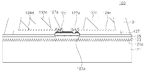
devices, in
which the transparent substrate has a concavo-convex pattern on a surface
facing the
light emitting devices.
[0010] Exemplary embodiments provide a pixel module, the pixel module
including: a
circuit board; and a plurality of unit pixels disposed on the circuit board,
in which each
of the unit pixels includes: a transparent substrate; a plurality of light
emitting devices
arranged on the transparent substrate; and an optical layer disposed between
the light
emitting devices and the transparent substrate, and transmitting light emitted
from the
light emitting devices, in which the transparent substrate has a concavo-
convex
pattern on a surface facing the light emitting devices.
[0011] Exemplary embodiments provide a displaying apparatus, the displaying
apparatus including: a panel substrate; and a plurality of pixel modules
arranged on
the panel substrate, in which each of the pixel modules includes: a circuit
board; and
a plurality of unit pixels disposed on the circuit board, in which each of the
unit pixels
includes: a transparent substrate; a plurality of light emitting devices
arranged on the
transparent substrate; and an optical layer disposed between the light
emitting devices
and the transparent substrate, and transmitting light emitted from the light
emitting
devices, in which the transparent substrate has a concavo-convex pattern on a
surface
facing the light emitting devices.
[Brief Descriptions of Drawings]
[0012] FIG. 1 is a schematic plan view illustrating a displaying apparatus
according to
3
Date Recue/Date Received 2022-08-01
CA 03169833 2022-08-01
one or more embodiments.
[0013] FIG. 2A is a schematic plan view illustrating a light emitting device
according
to one or more embodiments.
[0014] FIG. 2B is a schematic cross-sectional view taken along line A-A of
FIG. 2A.
[0015] FIG. 3A is a schematic plan view illustrating a unit pixel according to
one or
more embodiments.
[0016] FIG. 3B is a schematic cross-sectional view taken along line B-B of
FIG. 3A
[0017] FIG. 4A is a schematic plan view illustrating a pixel module according
to one
or more embodiments.
[0018] FIG. 4B is a schematic cross-sectional view taken along line C-C of
FIG. 4A
[0019] FIG. 4C is a schematic rear view illustrating a pixel module according
to one
or more embodiments.
[0020] FIG. 4D is a schematic circuit diagram illustrating a pixel module
according to
one or more embodiments.
[0021] FIG. 4E is a schematic circuit diagram illustrating a pixel module
according to
one or more embodiments.
[0022] FIGS. 5A through 5K are schematic cross-sectional views illustrating a
method
of transferring light emitting devices according to one or more embodiments,
where:.
[0023] FIGS. 6A through 6L are schematic cross-sectional views illustrating a
method
of transferring light emitting devices according to one or more embodiments,
where:.
[0024] FIGS. 7A through 7K are schematic cross-sectional views illustrating a
method
of transferring light emitting devices according to one or more embodiments.
[0025] FIG. 8 is a schematic cross-sectional view illustrating a unit pixel
according to
one or more embodiments.
4
Date Recue/Date Received 2022-08-01
CA 03169833 2022-08-01
[0026] FIG. 9 is a schematic cross-sectional view illustrating a pixel module
according
to one or more embodiments.
[0027] FIG. 10 is a schematic cross-sectional view illustrating a unit pixel
according
to one or more embodiments.
[0028] FIGs. 11A, 11B, 11C, 11D, 11E, 11F, and 11G are schematic plan views
illustrating various types of windows, where:
[0029] FIG. 12 is a graph illustrating viewing angle characteristics of light
according
to a presence or absence of a concavo-convex pattern on a transparent
substrate.
[Best Mode]
[0030] Hereinafter, embodiments will be described in detail with reference to
the
accompanying drawings. The following embodiments are provided by way of
example so as to fully convey the spirit of the present disclosure to those
skilled in the
art to which the present disclosure pertains. Accordingly, the present
disclosure is not
limited to the embodiments disclosed herein and can also be implemented in
different
forms. In the drawings, widths, lengths, thicknesses, and the like of elements
can be
exaggerated for clarity and descriptive purposes. When an element or layer is
referred to as being "disposed above" or "disposed on" another element or
layer, it can
be directly "disposed above" or "disposed on" the other element or layer or
intervening
elements or layers can be present. Throughout the specification, like
reference
numerals denote like elements having the same or similar functions.
[0031] A unit pixel according to one or more embodiments includes a
transparent
substrate, a plurality of light emitting devices arranged on the transparent
substrate,
and an optical layer disposed between the light emitting devices and the
transparent
substrate and transmitting light emitted from the light emitting devices. The
Date Recue/Date Received 2022-08-01
CA 03169833 2022-08-01
transparent substrate has a concavo-convex pattern on a surface facing the
light
emitting devices.
[0032] Viewing angles of light emitted from the light emitting devices may be
set to be
substantially uniform due to the concavo-convex pattern. The concavo-convex
pattern may increase the viewing angles of light emitted from the light
emitting devices.
[0033] Each of the plurality of light emitting devices may have a roughness on
a
surface facing the transparent substrate. The roughness improves light
extraction
efficiency of the light emitting device by reducing total internal reflection
due to a
difference in refractive index between the light emitting device and the
optical layer.
[0034] In some forms, the plurality of light emitting devices may include at
least three
light emitting devices emitting light of different colors from one another,
and the at least
three light emitting devices may be arranged in a line.
[0035] The optical layer is not particularly limited as long as it is an
optically
transparent material, and may be gas, liquid or solid. In at least one
variant, the light
emitting devices may be coupled to the transparent substrate by a coupler such
as a
spacer, and a region between the light emitting devices and the transparent
substrate
may be filled with gas or liquid. Accordingly, the optical layer may be formed
of gas
or liquid transparent to light.
[0036] In another variant, the optical layer may be an adhesive layer. The
light
emitting devices may be attached to the transparent substrate by the adhesive
layer.
[0037] Moreover, the unit pixel may further include: a step adjustment layer
covering
the light emitting device and adhered to the adhesive layer; and connection
layers
disposed on the step adjustment layer, and electrically connected to the light
emitting
devices.
6
Date Recue/Date Received 2022-08-01
CA 03169833 2022-08-01
[0038] In one or more embodiments, the plurality of light emitting devices may
include
light emitting devices emitting red, green, and blue light.
[0039] Each of the light emitting devices may include a light emitting
structure
including a first conductivity type semiconductor layer, a second conductivity
type
semiconductor layer, and an active layer interposed between the first and
second
conductivity type semiconductor layers, and a first electrode pad and a second
electrode pad disposed on the light emitting structure., The step adjustment
layer may
have openings exposing the first and second electrode pads, and the connection
layers may be electrically connected to the first and second electrode pads
through
the openings of the step adjustment layer.
[0040] The unit pixel may further include a protection layer covering the step
adjustment layer and contact layers, and the protection layer may have
openings
located on the contact layers.
[0041] Moreover, the light emitting device may further include bumps disposed
in the
openings of the protection layer, and the bumps may be electrically connected
to the
contact layers, respectively.
[0042] The light emitting device may further include a light blocking layer
disposed
between the optical layer and the transparent substrate, and the light
blocking layer
may have windows configured to transmit light generated from the light
emitting
devices.
[0043] In at least one variant, at least one of the windows may have an
extension
extending in a direction perpendicular to a direction in which the light
emitting devices
are arranged.
[0044] A viewing angle of light emitted from a corresponding light emitting
device may
7
Date Recue/Date Received 2022-08-01
CA 03169833 2022-08-01
be increased by the extension.
[0045] In another variant, the window may have an extension extending in the
diagonal direction.
[0046] In yet another variant, a plurality of windows may be arranged
corresponding
to each of the light emitting devices.
[0047] In further another variant, the concavo-convex pattern of the
transparent
substrate may be formed on an entire surface of the transparent substrate. In
another variant, the concavo-convex pattern of the transparent substrate may
be
disposed corresponding to the windows.
[0048] A pixel module according to one or more embodiments includes: a circuit
board; and a plurality of unit pixels disposed on the circuit board, in which
each of the
unit pixels includes a transparent substrate, a plurality of light emitting
devices
arranged on the transparent substrate, and an optical layer disposed between
the light
emitting devices and the transparent substrate, and transmitting light emitted
from the
light emitting devices., The transparent substrate has a concavo-convex
pattern on a
surface facing the light emitting devices.
[0049] Each of the plurality of light emitting devices may have a roughness on
a
surface facing the transparent substrate.
[0050] In addition, the unit pixel may further include a light blocking layer
disposed
between the optical layer and the transparent substrate, and the light
blocking layer
may include windows configured to transmit light generated from the light
emitting
devices.
[0051] In one or more embodiments, the concavo-convex pattern of the
transparent
substrate may be disposed corresponding to the windows.
8
Date Recue/Date Received 2022-08-01
CA 03169833 2022-08-01
[0052] In one or more embodiments, the optical layer may be an adhesive layer.
[0053] Moreover, the unit pixel may further include a step adjustment layer
covering
the light emitting device and adhered to the adhesive layer, connection layers
disposed on the step adjustment layer, and electrically connected to the light
emitting
devices, and a protection layer covering the step adjustment layer and contact
layers.
Furthermore, the protection layer may have openings located on the contact
layers.
[0054] The plurality of light emitting devices may include at least three
light emitting
devices emitting light of different colors from one another, and the at least
three light
emitting devices may be arranged in a line.
[0055] A displaying apparatus according to one or more embodiments includes: a
panel substrate, and a plurality of pixel modules arranged on the panel
substrate.
Each of the pixel modules includes a circuit board, and a plurality of unit
pixels
disposed on the circuit board. Each of the unit pixels includes a transparent
substrate,
a plurality of light emitting devices arranged on the transparent substrate,
and an
optical layer disposed between the light emitting devices and the transparent
substrate
and transmitting light emitted from the light emitting devices. The
transparent
substrate has a concavo-convex pattern on a surface facing the light emitting
devices.
[0056] Hereinafter, exemplary embodiments will be described in detail with
reference
to the accompanying drawings.
[0057] FIG. 1 is a schematic plan view illustrating a displaying apparatus
according to
one or more embodiments.
[0058] Referring to FIG. 1, a displaying apparatus 10000 includes a panel
substrate
2100 and a plurality of pixel modules 1000.
[0059] The displaying apparatus 10000 is not particularly limited, but may
include a
9
Date Recue/Date Received 2022-08-01
CA 03169833 2022-08-01
Virtual Reality (VR) displaying apparatus such as a micro LED TV, a smart
watch, a
VR headset, or an Augmented Reality (AR) displaying apparatus such as
augmented
reality glasses.
[0060] The panel substrate 2100 may include a circuit for passive matrix
driving or
active matrix driving. In one or more embodiments, the panel substrate 2100
may
include interconnection lines and resistors, and in another exemplary
embodiment, the
panel substrate 2100 may include interconnection lines, transistors, and
capacitors.
The panel substrate 2100 may also have pads that are capable of being
electrically
connected to the disposed circuit on an upper surface thereof.
[0061] The plurality of pixel modules 1000 is arranged on the panel substrate
2100.
Each of the pixel modules 1000 may include a circuit board and a plurality of
unit
pixels 100 disposed on the circuit board.
[0062] In addition, each of the unit pixels 100 includes a plurality of light
emitting
devices 10a, 10b, and 10c. The light emitting devices 10a, 10b, and 10c may
emit
light of different colors from one another. In some forms, the light emitting
devices
10a, 10b, and 10c in each of the unit pixels 100 may be arranged as shown in
FIG. 1.
In other forms, the light emitting devices 10a, 10b, and 10c may be arranged
in the
vertical direction with respect to a display screen on which an image is
implemented.
However, the inventive concepts are not limited thereto, and the light
emitting devices
10a, 10b, and 10c may be arranged in a lateral direction with respect to the
display
screen on which the image is implemented.
[0063] Hereinafter, each element of the displaying apparatus 10000 will be
described
in detail in the order of the light emitting devices 10a, 10b, and 10c, the
unit pixel 100,
and the pixel module 1000 that are disposed in the displaying apparatus 10000.
Date Recue/Date Received 2022-08-01
CA 03169833 2022-08-01
[0064] First, FIG. 2A is a schematic plan view illustrating a light emitting
device
according to one or more embodiments, and FIG. 2B is a schematic cross-
sectional
view taken along line A-A of FIG. 2A. Herein, the light emitting device 10a is
described in detail, and to the extent that the light emitting devices 10b and
10c have
similar structures, repeated descriptions thereof will be omitted.
[0065] Referring to FIGs. 2A and 2B, the light emitting device 10a includes a
light
emitting structure including a first conductivity type semiconductor layer 21,
an active
layer 23, and a second conductivity type semiconductor layer 25. Further, the
light
emitting device 10a may include an ohmic contact layer 27, an insulation layer
29, a
first electrode pad 31, and a second electrode pad 33.
[0066] The light emitting structure, that is, the first conductivity type
semiconductor
layer 21, the active layer 23, and the second conductivity type semiconductor
layer 25
may be grown on a substrate. The substrate may be various substrates that are
used
to grow semiconductors, such as gallium nitride substrate, GaAs substrate, Si
substrate, sapphire substrate, especially patterned sapphire substrate. The
growth
substrate may be separated from the semiconductor layers using a process such
as
a mechanical grinding, a laser lift off, a chemical lift off process, or the
like. However,
the inventive concepts are not limited thereto, and, in some exemplary
embodiments,
a portion of the substrate may remain as at least a portion of the first
conductivity type
semiconductor layer 21.
[0067] When the light emitting device 10a emits red light according to one or
more
embodiments, the semiconductor layers may include aluminum gallium arsenide
(AlGaAs), gallium arsenide phosphide (GaAsP), aluminum gallium indium
phosphide
(AlGaInP), or gallium phosphide (GaP).
11
Date Recue/Date Received 2022-08-01
CA 03169833 2022-08-01
[0068] When the light emitting device 10b emits green light according to one
or more
embodiments, the semiconductor layers may include indium gallium nitride
(InGaN),
gallium nitride (GaN), gallium phosphide (GaP), aluminum gallium indium
phosphide
(AlGaInP), or aluminum gallium phosphide (AlGaP).
[0069] When the light emitting device 10c emits blue light according to one or
more
embodiments, the semiconductor layers may include gallium nitride (GaN),
indium
gallium nitride (InGaN), or zinc selenide (ZnSe).
[0070] The first conductivity type and the second conductivity type have
opposite
polarities, when the first conductivity type is an n-type, the second
conductivity type
becomes a p-type, and, when the second conductivity type is a p-type, the
second
conductivity type becomes an n-type.
[0071] The first conductivity type semiconductor layer 21, the active layer
23, and the
second conductivity type semiconductor layer 25 may be grown on the substrate
in a
chamber using a known process such as metal organic chemical vapor deposition
(MOCVD) process. In addition, the first conductivity type semiconductor layer
21
includes n-type impurities (e.g., Si, Ge, and Sn), and the second conductivity
type
semiconductor layer 25 includes p-type impurities (e.g., Mg, Sr, and Ba). In
one or
more embodiments, the first conductivity type semiconductor layer 21 may
include
GaN or AlGaN containing Si as a dopant, and the second conductivity type
semiconductor layer 25 may include GaN or AlGaN containing Mg as a dopant.
[0072] Although the first conductivity type semiconductor layer 21 and the
second
conductivity type semiconductor layer 25 are shown as single layers in the
drawings,
these layers may be multiple layers, and may also include a superlattice
layer. The
active layer 23 may include a single quantum well structure or a multiple
quantum well
12
Date Recue/Date Received 2022-08-01
CA 03169833 2022-08-01
structure, and a composition ratio of a nitride-based semiconductor may be
adjusted
to emit a desired wavelength. For example, the active layer 23 may emit blue
light,
green light, red light, or ultraviolet light.
[0073] The second conductivity type semiconductor layer 25 and the active
layer 23
may have a mesa M structure and may be disposed on the first conductivity type
semiconductor layer 21. The mesa M may include the second conductivity type
semiconductor layer 25 and the active layer 23, and may include a portion of
the first
conductivity type semiconductor layer 21 as shown in FIG. 2B. The mesa M may
be
disposed on the portion of the first conductivity type semiconductor layer 21,
and an
upper surface of the first conductivity type semiconductor layer 21 may be
exposed
around the mesa M.
[0074] Meanwhile, the first conductivity type semiconductor layer 21 may have
a
roughness 21p due to surface texturing. Surface texturing may be carried out
by
patterning, for example, using a dry or wet etching process. For example, cone-
shaped protrusions may be formed, an elevation of the cone may be about 2 pm
to
about 3 pm, a distance between the cones may be about 1.5 pm to about 2 pm,
and
a diameter of a bottom of the cone may be about 3 pm to about 5 pm. The cone
may
also be truncated, in which a diameter of an upper surface of the cone may be
about
2 pm to about 3 pm. By forming roughness on the surface of the first
conductivity
type semiconductor layer 21, total internal reflection may be reduced, thereby
increasing light extraction efficiency. Surface texturing may be performed on
the first
conductivity type semiconductor layers in all of the first, second, and third
light emitting
devices 10a, 10b, and 10c, but the inventive concepts are not limited thereto,
and, in
some exemplary embodiments, surface texturing may not be performed in some of
the
13
Date Recue/Date Received 2022-08-01
CA 03169833 2022-08-01
light emitting devices.
[0075] In addition, the mesa M may have a through hole 25a exposing the first
conductivity type semiconductor layer 21. The through hole 25a may be disposed
close to one edge of the mesa M, but is not limited thereto, and, in some
exemplary
embodiments, the through hole 25a may be disposed at a center of the mesa M.
[0076] The ohmic contact layer 27 is disposed on the second conductivity type
semiconductor layer 25 to be in ohmic contact with the second conductivity
type
semiconductor layer 25. The ohmic contact layer 27 may be formed of a single
layer
or multiple layers, and may be formed of a transparent conductive oxide film
or a metal
film. For example, the transparent conductive oxide film may include ITO, ZnO,
or
the like, and the metal film may include a metal such as Al, Ti, Cr, Ni, Au,
or the like
and alloys thereof.
[0077] The insulation layer 29 covers the mesa M and the ohmic contact layer
27.
The insulation layer 29 may further cover upper and side surfaces of the first
conductivity type semiconductor layer 21 exposed around the mesa M. The
insulation layer 29 may have an opening 29a exposing the ohmic contact layer
27 and
an opening 29b exposing the first conductivity type semiconductor layer 21 in
the
through hole 25a. The insulation layer 29 may be formed of a single layer or
multiple
layers of a silicon oxide film or a silicon nitride film. The insulation layer
29 may also
include an insulation reflector, such as a distributed Bragg reflector.
[0078] The first electrode pad 31 and the second electrode pad 33 are disposed
on
the insulation layer 29. The second electrode pad 33 may be electrically
connected
to the ohmic contact layer 27 through the opening 29a, and the first electrode
pad 31
may be electrically connected to the first conductivity type semiconductor
layer 21
14
Date Recue/Date Received 2022-08-01
CA 03169833 2022-08-01
through the opening 29b.
[0079] The first and/or second electrode pads 31 and 33 may be formed of a
single
layer or a multiple layer of metal. As a material of the first and/or second
electrode
pads 31 and 33, a metal such as Al, Ti, Cr, Ni, Au, or the like and an alloy
thereof or
the like may be used.
[0080] Although the light emitting device 10a according to the exemplary
embodiment
has been briefly described with reference to the drawings, the light emitting
device 10a
may further include a layer having additional functions in addition to the
above-
described layers. For example, various layers such as a reflective layer for
reflecting
light, an additional insulation layer for insulating a specific element, and a
solder
preventing layer for preventing diffusion of solder may be further included.
[0081] When a flip chip type light emitting device is formed, the mesa may be
formed
to have various shapes, and the locations and shapes of the first and second
electrode
pads 31 and 33 may also have various modifications. In addition, the ohmic
contact
layer 27 may be omitted, and the second electrode pad 33 may directly contact
the
second conductivity type semiconductor layer 25. Although the first electrode
pad 31
is shown as being directly connected to the first conductivity type
semiconductor layer
21, the contact layer may be formed first on the first conductivity type
semiconductor
layer 21 exposed to the through hole 25a, and the first electrode pad 31 may
be
connected to the contact layer.
[0082] FIG. 3A is a schematic plan view illustrating a unit pixel 100
according to one
or more embodiments, and FIG. 3B is a schematic cross-sectional view taken
along
line B-B of FIG. 3A.
[0083] Referring to FIG. 3A and FIG. 3B, the unit pixel 100 may include a
transparent
Date Recue/Date Received 2022-08-01
CA 03169833 2022-08-01
substrate 121, a first, second, and third light emitting devices 10a, 10b, and
10c, a
light blocking layer 123, and an adhesive layer 125, a step adjustment layer
127,
connection layers 129a, 129b, 129c, and 129d, bumps 133a, 133b, 133c, and
133d,
and a protection layer 131.
[0084] The unit pixel 100 provides a single pixel including the first, second,
and third
light emitting devices 10a, 10b, and 10c. The first, second, and third light
emitting
devices 10a, 10b, and 10c emit light of different colors, and the first,
second, and third
light emitting devices 10a, 10b, and 10c correspond to subpixels,
respectively.
[0085] The transparent substrate 121 is a light-transmitting substrate such as
PET,
glass substrate, quartz, sapphire substrate, or the like. The transparent
substrate
121 is disposed on a light emitting surface of the displaying apparatus (10000
in FIG.
1), and light emitted from the light emitting devices 10a, 10b, and 10c is
emitted to the
outside through the transparent substrate 121. The transparent substrate 121
may
include a concavo-convex pattern 121p on a surface facing the light emitting
devices
10a, 10b, and 10c. The concavo-convex pattern 121p scatters light emitted from
the
light emitting devices 10a, 10b, and 10c to increase viewing angles. In
addition, light
emitted from the light emitting devices 10a, 10b, and 10c having different
viewing angle
characteristics may be emitted as light having substantially uniform viewing
angles by
the concavo-convex pattern 121p. Accordingly, occurrence of a color difference
depending on an angle at which a user sees a display image may be
substantially
reduced.
[0086] The concavo-convex pattern 121p may be regular or irregular. The
concavo-
convex pattern 121P may have a pitch of about 3 pm, a diameter of about 2.8
pm, and
an elevation of about 1.8 pm, for example. The concavo-convex pattern 121p may
16
Date Recue/Date Received 2022-08-01
CA 03169833 2022-08-01
be a pattern generally applied to a patterned sapphire substrate, but is not
limited
thereto.
[0087] The transparent substrate 121 may also include an anti-reflection
coating, may
include an anti-glare layer, or may be treated with an anti-glare treatment.
The
transparent substrate 121 may have a thickness of about 50 pm to about 300 pm
for
example.
[0088] As the transparent substrate 121 is disposed on the light emitting
surface, the
transparent substrate 121 does not include a circuit such as a connection
circuit, a
driving circuit, etc. However, the inventive concepts are not limited thereto,
and, in
some exemplary embodiments, the transparent substrate 121 may include
circuit(s).
[0089] Although a single unit pixel 100 is illustrated to be formed on a
single
transparent substrate 121, a plurality of unit pixels 100 may be formed on the
single
transparent substrate 121.
[0090] The light blocking layer 123 may include an absorbing material which
absorbs
light such as carbon black. The light absorbing material may prevent light
generated
in the light emitting devices 10a, 10b, and 10c from leaking from a region
between the
transparent substrate 121 and the light emitting devices 10a, 10b, and 10c
toward a
side surface thereof, and may improve contrast of the displaying apparatus.
[0091] The light blocking layer 123 may have a window 123a for a light path,
so that
light generated in the light emitting devices 10a, 10b, and 10c is incident on
the
transparent substrate 121. A width of the window 123a may be smaller than that
of
the light emitting device, but is not limited thereto, and, in some exemplary
embodiments, may be greater than or equal to the width of the light emitting
device.
[0092] The window 123a of the light blocking layer 123 also defines an
arrangement
17
Date Recue/Date Received 2022-08-01
CA 03169833 2022-08-01
location of the light emitting devices 10a, 10b, and 10c. As such, separate
arrangement markers for defining arrangement locations of the light emitting
devices
10a, 10b, and 10c may be omitted. However, the inventive concepts are not
limited
thereto, and, in some exemplary embodiments, the arrangement markers may be
disposed on the transparent substrate 121, or on the light blocking layer 123
or the
adhesive layer 125 to provide locations to arrange the light emitting devices
10a, 10b,
and 10c.
[0093] Viewing angles of light emitted from the light emitting devices 10a,
10b, and
10c may be adjusted according to a shape of the window 123a formed on the
light
blocking layer 123. This will be described in detail later with reference to
FIGs. 11A
through 11F.
[0094] The adhesive layer 125 is attached onto the transparent substrate 121.
The
adhesive layer 125 may cover the light blocking layer 123. The adhesive layer
125
may be attached onto an entire surface of the transparent substrate 121, but
is not
limited thereto, and, in some exemplary embodiments, the adhesive layer 125
may be
attached to a portion of the transparent substrate 121 to expose a region near
an edge
of the transparent substrate 121. The adhesive layer 125 is used to attach the
light
emitting devices 10a, 10b, and 10c to the transparent substrate 121. The
adhesive
layer 125 may fill the window 123a formed in the light blocking layer 123.
[0095] The adhesive layer 125 may be formed as a light-transmitting layer, and
transmits light emitted from the light emitting devices 10a, 10b, and 10c. The
adhesive layer 125 may be formed using an organic adhesive. For example, the
adhesive layer 125 may be formed using a transparent epoxy. In addition, the
adhesive layer 125 may include a diffuser such as SiO2, TiO2, ZnO, or the like
to diffuse
18
Date Recue/Date Received 2022-08-01
CA 03169833 2022-08-01
light. The light diffusing material prevents the light emitting devices 10a,
10b and 10c
from being observed from the light emitting surface.
[0096] The first, second, and third light emitting devices 10a, 10b, and 10c
are
disposed on the transparent substrate 121. The first, second, and third light
emitting
devices 10a, 10b, and 10c may be attached to the transparent substrate 121 by
the
adhesive layer 125. The first, second, and third light emitting devices 10a,
10b, and
10c may be disposed to correspond to the windows 123a of the light blocking
layer
123. When the light blocking layer 123 is omitted, the arrangement markers may
be
added to provide the arrangement locations of the light emitting devices 10a,
10b, and
10c.
[0097] The first, second, and third light emitting devices 10a, 10b, and 10c
may be,
for example, red light emitting devices, green light emitting devices, and
blue light
emitting devices. Since specific configurations of each of the first, second,
and third
light emitting devices 10a, 10b, and 10c are the same as those described with
reference to FIG. 2A and FIG. 2B, detailed descriptions thereof will be
omitted.
[0098] The first, second, and third light emitting devices 10a, 10b, and 10c
may be
arranged in a line, as shown in FIG. 3A. In particular, in a case that the
transparent
substrate 121 is a sapphire substrate, the sapphire substrate may include
clean-cut
surfaces (e.g., m-plane) and non-clean-cut surfaces (e.g., a-plane) due to a
location
of a crystal plane along a cutting direction. For example, when the sapphire
substrate
is cut into a quadrangular shape, two cutting planes on both sides thereof
(e.g., m-
plane) may be cut cleanly along the crystal plane, and two remaining cutting
planes
(e.g., a-plane) disposed in a direction perpendicular to the cutting planes
may not be
cut clean. In this case, the clean-cut surfaces of the sapphire substrate 121
may be
19
Date Recue/Date Received 2022-08-01
CA 03169833 2022-08-01
flush with an arrangement direction of the light emitting devices 10a, 10b,
and 10c.
For example, in FIG. 3A, the clean-cut surfaces (e.g., m-plane) may be
disposed up
and down, and the two remaining cut surfaces (e.g., a-plane) may be disposed
left
and right.
[0099] The first, second, and third light emitting devices 10a, 10b, and 10c
may be
those described above with reference to FIG. 2A and FIG. 2B, but the inventive
concepts are not limited thereto, and various light emitting devices having a
lateral or
flip chip structure may be used.
[0100] The step adjustment layer 127 covers the first, second, and third light
emitting
devices 10a, 10b, and 10c. The step adjustment layer 127 has openings 127a
exposing the first and second electrode pads 31 and 33 of the light emitting
devices
10a, 10b, and 10c. The step adjustment layer 127 is required to form the
connection
layers 129a, 129b, 129c, and 129d and the bumps 133a, 133b, 133c, and 133d. In
particular, the step adjustment layer 127 may be formed to equalize elevations
of
locations where the bumps 133a, 133b, 133c, and 133d are formed. The step
adjustment layer 127 may be formed of, for example, photosensitive polyimide.
[0101] The step adjustment layer 127 may be disposed in a region surrounded by
an
edge of the adhesive layer 125, but the inventive concepts are not limited
thereto.
For example, the step adjustment layer 127 may be formed to partially expose
the
edge of the adhesive layer 125.
[0102] The connection layers 129a, 129b, 129c, and 129d are formed on the step
adjustment layer 127. The connection layers 129a, 129b, 129c, and 129d may be
connected to the first and second electrode pads 31 and 33 of the first,
second, and
third light emitting devices 10a, 10b, and 10c through the openings 127a of
the step
Date Recue/Date Received 2022-08-01
CA 03169833 2022-08-01
adjustment layer 127.
[0103] For example, the connection layer 129a may be electrically connected to
a first
conductivity type semiconductor layer of the first light emitting device 10a,
the
connection layer 129b may be electrically connected to a first conductivity of
the
second light emitting device 10b, the connection layer 129c may be
electrically
connected to a first conductivity type semiconductor layer of the third light
emitting
device 10c, and the connection layer 129d may be commonly electrically
connected
to second conductivity type semiconductor layers of the first, second, and
third light
emitting devices 10a, 10b, and 10c. The connection layers 129a, 129b, 129c,
and
129d may be formed together on the step adjustment layer 127, and may include,
for
example, Au.
[0104] The bumps 133a, 133b, 133c, and 133d are formed on the connection
layers
129a, 129b, 129c, and 129d, respectively. For example, the first bump 133a may
be
electrically connected to the first conductivity type semiconductor layer of
the first light
emitting device 10a through the connection layer 129a, the second bump 133b
may
be electrically connected to the first conductivity type semiconductor layer
of the
second light emitting device 10b through the connection layer 129b, and the
third
bump 133c may be electrically connected to the first conductivity type
semiconductor
layer of the third light emitting device 10c through the connection layer
129c. The
fourth bump 133d may be commonly electrically connected to the second
conductivity
type semiconductor layers of the first, second, and third light emitting
devices 10a,
10b, and 10c through the connection layer 129d. The bumps 133a, 133b, 133c,
and
133d may be formed of, for example, a metal and/or a metal alloy such as AuSn,
SnAg,
Sn, CuSn, CuN, CuAg, Sb, Ni, Zn, Mo, Co, solder, or the like.
21
Date Recue/Date Received 2022-08-01
CA 03169833 2022-08-01
[0105] The protection layer 131 may cover side surfaces of the bumps 133a,
133b,
133c, and 133d, and may cover the step adjustment layer 127. In addition, the
protection layer 131 may cover the adhesive layer 125 exposed around the step
adjustment layer 127. The protection layer 131 may be formed of, for example,
a
photosensitive solder resist (PSR), and, accordingly, the protection layer 131
may be
patterned first through photolithography and development processes, and then
the
bumps 133a, 133b, 133c, and 133d may be formed. To this end, the protection
layer
131 may be formed to have openings exposing the contact layers 129a, 129b,
129c,
and 129d, and the bumps 133a, 133b, 133c, and 133d may be formed in the
openings
of the protection layer 131. The bumps 133a, 133b, 133c, and 133d may be
omitted.
[0106] The protection layer 131 may be formed of a light absorbing material
such as
a white reflective material or a black epoxy to prevent light leakage.
[0107] In the illustrated exemplary embodiment, the light emitting devices
10a, 10b,
and 10c are described as being attached to the transparent substrate 121 by
the
adhesive layer 125, but the light emitting devices 10a, 10b, and 10c may be
coupled
to the transparent substrate 121 using another coupler instead of the adhesive
layer
125. For example, the light emitting devices 10a, 10b, and 10c may be coupled
to
the transparent substrate 121 using spacers, and thus, gas or liquid may be
filled in a
region between the light emitting devices 10a, 10b, and 10c and the
transparent
substrate 121. An optical layer that transmits light emitted from the light
emitting
devices 10a, 10b, and 10c may be formed by the gas or liquid. The adhesive
layer
125 described above is also an example of the optical layer. Herein, the
optical layer
is formed of a material such as gas, liquid, or solid, different from those of
the light
emitting devices 10a, 10b, and 10c, and thus, is distinguished from the
materials of
22
Date Recue/Date Received 2022-08-01
CA 03169833 2022-08-01
the semiconductor layers in the light emitting devices 10a, 10b, and 10c.
[0108] FIG. 4A is a schematic plan view illustrating a pixel module 1000
according to
one or more embodiments, FIG. 4B is a schematic cross-sectional view taken
along
line C-C of FIG. 4A, FIG. 4C is a rear view of the pixel module 1000, and FIG.
4D is a
circuit diagram of the pixel module 1000.
[0109] Referring to FIG. 4A and 4B, the pixel module 1000 includes a circuit
board
1001 and unit pixels 100 arranged on the circuit board 1001. The pixel module
1000
may further include a cover layer 1010 covering the unit pixels 100.
[0110] The circuit board 1001 may have a circuit for electrically connecting a
panel
substrate 2100 and light emitting devices 10a, 10b, and 10c. The circuit in
the circuit
board 1001 may be formed to have a multilayer structure. The circuit board
1001
may also include a passive circuit for driving the light emitting devices 10a,
10b, and
10c in a passive matrix driving manner or an active circuit for driving the
light emitting
devices 10a, 10b, and 10c in an active matrix driving manner. The circuit
board 1001
may include pads 1003 exposed on a surface thereof. The pads 1003 may be
arranged corresponding to bumps in the unit pixels 100 to be mounted thereon.
[0111] Since a detailed configuration of the unit pixels 100 is the same as
that
described with reference to FIGS. 3A and 3B, detailed descriptions thereof
will be
omitted to avoid redundancy. The unit pixels 100 may be arranged on the
circuit
board 1001. The unit pixels 100 may be arranged in a 2x2 matrix as shown in
FIG.
4A, but the inventive concepts are not limited thereto, and, in some exemplary
embodiments, the unit pixels 100 may be arranged in various matrices such as
2x3,
3x3, 4x4, 5x5, or the like.
[0112] The unit pixels 100 are bonded to the circuit board 1001 by a bonding
material
23
Date Recue/Date Received 2022-08-01
CA 03169833 2022-08-01
1005. For example, the bonding material 1005 may bond the bumps 133a, 133b,
133c, and 133d to the pads 1003. When the bumps 133a, 133b, 133c, and 133d are
formed of solder, the bonding material 1005 may be omitted.
[0113] The cover layer 1010 covers a plurality of unit pixels 100. The cover
layer
1010 may improve contrast of the displaying apparatus by preventing optical
interference between the unit pixels 100.
[0114] The cover layer 1010 may be formed of, for example, a dry-film type
solder
resist (DFSR), a photoimageable solder resist (PSR), a black material (BM), an
epoxy
molding compound (EMC), or the like. The cover layer 1010 may be formed using,
for example, a technique such as lamination, spin coating, slit coating,
printing, or the
like.
[0115] A displaying apparatus 10000 may be provided by mounting the pixel
modules
1000 on the panel substrate 2100 of FIG. 1 as shown in FIG. 4A and FIG. 4B.
The
circuit board 1001 has bottom pads connected to the pads 1003. The bottom pads
may be arranged in a one-to-one correspondence with the pads 1003, but the
number
of the bottom pads may be reduced through a common connection. In this regard,
the pixel module 1000 having the unit pixels 100 arranged in a 2x2 matrix will
be
described with reference to FIG. 4C and FIG. 4D as an example.
[0116] FIG. 4C illustrates a rear view of the pixel module 1000, and bottom
pads Cl,
C2, R1, R2, G1, G2, B1, and B2 of the circuit board 1001 are illustrated.
Since the
pixel modules 1000 are arranged in a 2x2 matrix, a total of four pixel modules
are
arranged on the circuit board 1001. Three light emitting devices 10a, 10b, and
10c
and four bumps 133a, 133b, 133c, and 133d are disposed on each pixel module
1000.
Accordingly, sixteen pads 1003 corresponding to the bumps of the four unit
pixels 100
24
Date Recue/Date Received 2022-08-01
CA 03169833 2022-08-01
will be provided on the circuit board 1001. However, only eight bottom pads
may be
disposed, and the eight bottom pads may be connected to the panel substrate
2100
to individually drive each of the light emitting devices 10a, 10b, and 10c.
[0117] FIG. 4D illustrates a schematic circuit diagram in which each of the
light
emitting devices 10a, 10b, and 10c are connected to the bottom pads C1, C2,
R1, R2,
G1, G2, B1, and B2.
[0118] Referring to FIG. 4D, the bottom pad C1 is commonly connected to
cathodes
of the light emitting devices 10a, 10b, and 10c disposed in the left column,
and the
bottom pad C2 is commonly connected to cathodes of the light emitting devices
10a,
10b, and 10c disposed in the right column.
[0119] In the unit pixels 100 arranged in the upper row, a bottom pad R1 may
be
connected to anodes of the first light emitting devices 10a, a bottom pad G1
may be
connected to anodes of the second light emitting devices 10b, and a bottom pad
B1
may be connected to anodes of the third light emitting devices 10c.
[0120] In the unit pixels 100 arranged in the lower row, a bottom pad R2 may
be
connected to the anodes of the first light emitting devices 10a, a bottom pad
G2 may
be connected to the anodes of the second light emitting devices 10b, and a
bottom
pad B2 may be connected to the anodes of the third light emitting devices 10c.
[0121] Herein, the bottom pads R1, G1, B1, R2, G2, and B2 represent pads
connected to red, green, and blue light emitting devices, respectively.
However, the
order of arrangement of the red, green, and blue light emitting devices may be
changed, and, accordingly, locations to which the bottom pads R1, G1, B1, R2,
G2,
and B2 are connected may also be changed. For example, the circuit diagram of
FIG. 4D shows the bottom pads based on the assumption that the first light
emitting
Date Recue/Date Received 2022-08-01
CA 03169833 2022-08-01
devices 10a are red light emitting devices, the second light emitting devices
10b are
green light emitting devices, and the third light emitting devices 10c are
blue light
emitting devices. Alternatively, the first light emitting devices 10a may be
the blue
light emitting devices, and the third light emitting devices 10c may be the
red light
emitting devices, and, in this case, the locations of the bottom pads R1 and
R2 and
the bottom pads B1 and B2 may be interchanged.
[0122] According to the illustrated exemplary embodiment, since the bottom
pads C1
and C2 are commonly connected to the cathodes of the light emitting devices in
each
column, and each of the bottom pads R1, G1, B1, R2, B2, and G2 are connected
to
the anodes of the two light emitting devices, each of the light emitting
devices 10a,
10b, and 10c may be driven independently while reducing the total number of
the
bottom pads.
[0123] Although it is described and illustrated that the bottom pads C1 and C2
are
connected to the cathodes of the light emitting devices and the bottom pads
R1, G1,
B1, R2, B2 and G2 are connected to the anodes of the light emitting device in
the
illustrated exemplary embodiment, the bottom pads C1 and C2 may be connected
to
the anodes of the light emitting devices, and the bottom pads R1, G1, B1, R2,
B2 and
G2 may be connected to the cathodes of the light emitting device as shown in
FIG.
4E.
[0124] Herein, although the pixel module 1000 is described that the unit
pixels 100
are arranged in a 2x2 matrix, the number of the bottom pads may be reduced
using a
common connection circuit even when the unit pixels 100 are arranged in
another
matrix such as 3x3, 5x5, or the like.
[0125] The light emitting devices 10a, 10b, and 10c in the pixel module 1000
may be
26
Date Recue/Date Received 2022-08-01
CA 03169833 2022-08-01
individually driven by a driving IC disposed on the panel substrate 2100, and
images
may be implemented by a plurality of pixel modules 1000.
[0126] FIGs. 5A through 5K are schematic cross-sectional views illustrating a
method
of transferring light emitting devices according to one or more embodiments.
[0127] Referring to FIG. 5A, a light emitting device 10 is formed on a
substrate 51.
The substrate 51 may be a substrate that grows semiconductor layers of the
light
emitting device 10. The substrate 51 may be, for example, a sapphire substrate
or a
GaN substrate for growing an AlInGaN-based semiconductor layer, or a GaAs
substrate for growing AINGaP-based semiconductor layers. For example, when the
light emitting device 10 is a blue light emitting device or a green light
emitting device,
the sapphire substrate or the GaN substrate may be used, and, when the light
emitting
device 10 is a red light emitting device, the GaAs substrate may be used.
[0128] Referring to FIG. 5B, a first mask layer 53 is formed on the substrate
51 to
cover a plurality of light emitting devices 10. The first mask layer 53 may be
formed
to completely cover the plurality of light emitting devices 10, and may be
formed to
have a predetermined thickness on upper surfaces of the light emitting devices
10.
[0129] Referring to FIG. 5C, a plurality of holes Hs are formed in the first
mask layer
53. Each
of the plurality of holes Hs may be formed over the plurality of light
emitting
devices 10, and at least one hole H may be formed on each of the light
emitting devices
10. In the illustrated exemplary embodiment, three holes Hs are formed on each
of
the light emitting devices 10, and the three holes Hs are arranged
asymmetrically to
at least one direction where the light emitting devices 10 are arranged.
Herein, the
three holes Hs in the drwaing are arranged asymmetrically to a direction which
is
perpendicular to the direction where the light emitting devices 10 are
arranged.
27
Date Recue/Date Received 2022-08-01
CA 03169833 2022-08-01
[0130] The first mask layer 53 may be formed of a photosensitive material, and
the
plurality of holes Hs may be formed through a photolithography process. The
plurality
of holes Hs may be formed through an exposure and development processes, but
the
inventive concepts are not necessarily limited thereto, but an etching process
may be
used. The plurality of holes Hs may be formed to have a triangular shape as
shown
in the drawing. However, the number of holes Hs is not necessarily limited to
three.
[0131] Referring to FIG. 5D, a connection layer 55 is formed on the first mask
layer
53. The connection layer 55 is formed on the first mask layer 53 while filling
the
plurality of holes Hs formed in the first mask layer 53. Since at least one
hole H is
formed over each of the light emitting devices 10, the connection layer 55 may
be
connected to the light emitting device 10 through at least one hole H formed
over the
light emitting device 10. A connection portion 55a connected to the light
emitting
device 10 by filling the hole H is formed together while the connection layer
55 is
formed.
[0132] The connection layer 55 may be formed of an organic material such as
poly
dimethylpolysiloxane (PDMS), epoxy, acryl, color polyimide, or the like, but
it is not
limited thereto. Herein, the connection layer 55 may have a light
transmittance of
90% or more, and a refractive index may be about 1.4 to about 1.7.
[0133] Referring to FIG. 5E, a first temporary substrate 57 is coupled to an
upper
region of the connection layer 55. The first temporary substrate 57 may be a
polymer
substrate such as PET, PEN, PI sheet, or the like, or may be a substrate such
as glass,
PC, PMMA, or the like. When the first temporary substrate 57 is coupled to the
upper
region of the connection layer 55, bubbles generated in the connection layer
55 in a
vacuum state may be removed, and a hardening process of the connection layer
55
28
Date Recue/Date Received 2022-08-01
CA 03169833 2022-08-01
may be carried out at a temperature lower than a melting point of the first
mask layer
53. In
this process, the first temporary substrate 57 may be coupled to the
connection
layer 55.
[0134] When the first temporary substrate 57 is coupled to the connection
layer 55,
the substrate 51 is removed from the light emitting devices 10 as shown in
FIG. 5F.
The substrate 51 may be removed by a laser lift-off process or a wet etching
process.
For example, if the substrate 51 is a sapphire substrate, the substrate 51 may
be
removed by the laser lift-off process or a chemical lift-off process, and if
the substrate
51 is a GaAs substrate, the GaAs substrate may be removed by the wet etching
process.
[0135] Referring to FIG. 5G, in a state that the substrate 51 is removed, the
first mask
layer 53 is removed from the light emitting devices 10. The first mask layer
53 may
be removed using, for example, acetone, a dedicated striper, etching, or the
like.
Since the first mask layer 53 is removed, as shown in the drawing, each of the
light
emitting devices 10 is connected to the connection layer 55 through at least
one
connection portion 55a and maintained.
[0136] Referring to FIG. 5H, after the first mask layer 53 is removed from the
light
emitting devices 10, a second temporary substrate 59 is coupled to lower
surfaces of
the light emitting devices 10. The second temporary substrate 59 may be a
rubber
or UV sheet, or may be a polymer substrate such as PET, PEN, PI sheet, or the
like,
or a substrate such as glass, PC, PMMA, or the like.
[0137] When coupling the second temporary substrate 59 to the light emitting
devices
is completed, the light emitting devices 10 are removed from the connection
layer
55 using the second temporary substrate 59 as shown in FIG. 51. By applying an
29
Date Recue/Date Received 2022-08-01
CA 03169833 2022-08-01
external force in an opposite direction to the first temporary substrate 57,
i.e.,
downward, to the second temporary substrate 59 coupled to the light emitting
devices
10, the at least one connection portion 55a connected to the light emitting
devices 10
is cut, and the light emitting devices 10 are separated from the connection
layer 55.
[0138] The external force applied to the second temporary substrate 59 as
shown in
the drawing, may be applied in a direction perpendicular to the connection
layer 55 at
one side of the second temporary substrate 59. As such, each of the light
emitting
devices 10 may be separated from the connection layer 55 in such a manner that
the
at least one connection portion 55a connected to each of the light emitting
devices 10
is sequentially cut from one side of the second temporary substrate 59.
[0139] Referring to FIG. 5J, the light emitting devices 10 separated from the
connection layer 55 are disposed on the second temporary substrate 59 with a
predetermined interval. In the meantime, a connection tip 55b may be formed on
each of the light emitting devices 10 as a residue while the connection
portion 55a is
cut. Accordingly, the connection tip 55b is formed of the same material as the
connection layer 55, and formed while the connection portion 55a is cut by an
external
force, so that thicknesses of the connection tips 55b may be irregular and
different
from one another.
[0140] Referring to FIG. 5J and FIG. 5K, a portion of the light emitting
devices 10
disposed on the second temporary substrate 59 is transferred to another
substrate
using a picker 70. The picker 70 may include an elastomeric stamp, for
example.
[0141] The picker 70 picks up and transfers a portion of the plurality of
light emitting
devices 10, and selectively picks up the light emitting devices 10 in
accordance with
an interval between light emitting devices 10 which will be arranged on the
transparent
Date Recue/Date Received 2022-08-01
CA 03169833 2022-08-01
substrate 121. As such, as shown in the drawing, the picker 70 doesn't pick up
adjacent light emitting devices 10 together, but picks up the light emitting
devices 10
having a certain interval at a time. The interval between the light emitting
devices 10
picked up may vary depending on an interval between pixels in the transparent
substrate 121 onto which the light emitting devices 10 are to be transferred.
[0142] After the light emitting devices 10 are arranged on the transparent
substrate
121 to correspond to a plurality of unit pixels 100, the transparent substrate
121 may
be cut in each pixel unit to form the unit pixel 100. As such, the light
emitting devices
are transferred onto the transparent substrate 121 to correspond to each unit
pixel
100.
[0143] The picker 70 picks up the light emitting devices 10 to fit an interval
matching
an interval between the unit pixels 100, and one of the first light emitting
device 10a,
the second light emitting device 10b, and the third light emitting device 10c
may be
picked up to be arranged in a single unit pixel 100.
[0144] The light emitting devices 10 may be picked up in a state that the
first and
second electrode pads 31 and 33 are disposed thereon according to the
exemplary
embodiment, and may be also transferred to the transparent substrate 121 in
this
state. As such, light generated in the light emitting structure may be emitted
to the
outside through the transparent substrate 121. In another exemplary
embodiment,
the light emitting devices 10 may be mounted on a circuit board, and, in this
case, the
first and second electrode pads 31 and 33 may be mounted toward the circuit
board.
To do this, an additional temporary substrate may be used in a process of
mounting
the light emitting devices 10 on the circuit board using the picker 70.
More
particularly, the light emitting devices 10 picked up through the picker 70
may be first
31
Date Recue/Date Received 2022-08-01
CA 03169833 2022-08-01
arranged on the additional temporary substrate at the interval between the
unit pixels
100. Thereafter, the light emitting devices 10 disposed on the additional
temporary
substrate may be transferred to the circuit board at a time. As such, the
light emitting
devices 10 may be transferred, so that the first and second electrode pads 31
and 33
may be bonded to the circuit board.
[0145] FIGs. 6A through 6L are schematic cross-sectional views illustrating a
method
of transferring light emitting devices according to another exemplary
embodiment.
[0146] Referring to FIG. 6A, a light emitting device 10 is grown on a
substrate 51.
The substrate 51 may be a substrate that grows semiconductor layers of the
light
emitting device 10. In some embodiments, when the light emitting device 10 is
a blue
light emitting device or a green light emitting device, a sapphire substrate
or a GaN
substrate may be used, and, when the light emitting device 10 is a red light
emitting
device, a GaAs substrate may be used.
[0147] Referring to FIG. 6B, a first mask layer 53 is formed on the substrate
51 to
cover a plurality of light emitting devices 10. The first mask layer 53 may be
formed
to cover all of the plurality of light emitting devices 10, and may be formed
to have a
predetermined thickness on upper surfaces of the light emitting devices 10.
[0148] Subsequently, referring to FIG. 6C, a plurality of holes Hs are formed
in the
first mask layer 53. At least one hole H may be formed on each of the light
emitting
devices 10. According to the exemplary embodiment, three holes Hs are formed
on
each of the light emitting devices 10, and the three holes Hs are arranged
asymmetrically to at least one direction where the light emitting devices 10
are
arranged. Herein, the plurality of holes Hs in FIG. 6C are arranged
asymmetrically
to a direction which is perpendicular to the direction where the light
emitting devices
32
Date Recue/Date Received 2022-08-01
CA 03169833 2022-08-01
are arranged.
[0149] The first mask layer 53 may be formed of a photosensitive material, and
the
plurality of holes Hs may be formed through a photolithography process. For
example, the holes Hs may be formed through an exposure and development
processes, but it is not limited thereto, but an etching process may be used.
The
plurality of holes Hs may be formed in a triangular shape.
[0150] Referring to FIG. 6D, a connection layer 55 is formed on the first mask
layer
53. The connection layer 55 is formed on the first mask layer 53 while filling
the plurality
of holes Hs formed in the first mask layer 53. Since each of the plurality of
holes Hs
is formed over the light emitting device 10, the connection layer 55 may be
connected
to the light emitting devices 10 through at least one hole H formed over the
light
emitting device 10. A portion of the connection layer 55 may form a connection
portion 55a by filling the at least one hole H formed over the light emitting
device 10.
[0151] The connection layer 55 may be formed of an organic material such as
poly
dimethylpolysiloxane (PDMS), epoxy, acryl, color polyimide, or the like, but
it is not
limited thereto. Herein, the connection layer 55 may have a light
transmittance of
90% or more, and a refractive index may be about 1.4 to about 1.7.
[0152] Referring to FIG. 6E, a first temporary substrate 57 is coupled to an
upper
region of the connection layer 55. The first temporary substrate 57 may be a
polymer
substrate such as PET, PEN, PI sheet, or the like, or may be a substrate such
as glass,
PC, PMMA, or the like. A film layer 61 and a buffer layer 63 may be disposed
between the first temporary substrate 57 and the connection layer 55,
respectively.
For example, the film layer 61 may be disposed over the connection layer 55,
the
buffer layer 63 may be disposed over the film layer 61, and the first
temporary
33
Date Recue/Date Received 2022-08-01
CA 03169833 2022-08-01
substrate 57 may be disposed over the buffer layer 63. The buffer layer 63 may
be
formed of a material melted by heat or UV irradiation.
[0153] When the first temporary substrate 57 is coupled to the upper surface
of the
connection layer 55, bubbles generated in the connection layer 55 in a vacuum
state
may be removed, and a hardening process of the connection layer 55 may be
performed at a temperature lower than a melting point of the first mask layer
53. In
this process, the first temporary substrate 57 may be coupled to the
connection layer
55.
[0154] Referring to FIG. 6F, the substrate 51 is removed from the light
emitting
devices 10. The substrate 51 may be removed by a laser lift-off process or a
wet
etching process. For example, in a case of a sapphire substrate, it may be
removed
by the laser lift-off process or a chemical lift-off process, and a GaAs
substrate may
be removed by the wet etching process.
[0155] Referring to FIG. 6G, the first mask layer 53 is removed from the light
emitting
devices 10 in a state that the substrate 51 is removed. The first mask layer
53 may
be removed using, for example, acetone, a dedicated striper, dry etching, or
the like.
As such, the light emitting devices 10 are connected to the connection layer
55 through
at least one connection portion 55a connected to each of the light emitting
devices 10
and maintained as shown in the drawing.
[0156] Referring to FIG. 6H, the first temporary substrate 57 coupled to the
upper
surface of the connection layer 55 is removed. In some embodiments, the first
temporary substrate 57 may be removed by heat or UV irradiation. The first
temporary substrate 57 may be removed without damaging the film layer 61
because
the buffer layer 63 is formed of a material melted by heat or UV irradiation.
34
Date Recue/Date Received 2022-08-01
CA 03169833 2022-08-01
[0157] Referring to FIG. 61, a second temporary substrate 59 is coupled to a
lower
surface of the light emitting devices 10. The second temporary substrate 59
may be
a rubber or UV sheet, or may be a polymer substrate such as PET, PEN, PI
sheet, or
the like, or a substrate such as glass, PC, PMMA, or the like.
[0158] When the second temporary substrate 59 is coupled to the light emitting
devices 10, the light emitting devices 10 are removed from the connection
layer 55
using the second temporary substrate 59 as shown in FIG. 6J. By applying an
external force downward to the second temporary substrate 59 coupled to the
light
emitting devices, the at least one connection portion 55a connected to the
light
emitting devices 10 is cut, and the light emitting devices 10 are separated
from the
connection layer 55.
[0159] The external force applied to the second temporary substrate 59 as
shown in
the drawing, may be applied in a direction perpendicular to the connection
layer 55 at
one side of the second temporary substrate 59. As such, each of the light
emitting
devices 10 may be separated from the connection layer 55 in such a manner that
the
connection portions 55a connected to each of the light emitting devices 10 is
sequentially cut.
[0160] Referring to FIG. 6K, the light emitting devices 10 separated from the
connection layer 55 are disposed on the second temporary substrate 59 with a
predetermined interval. At least one connection tip 55b may be formed on each
of
the light emitting devices 10 as a residue while the connection portion 55a is
cut. The
connection tip 55b is formed of the same material as the connection layer 55,
and
formed while the connection portion 55a is cut by an external force, so that
thicknesses
of the connection tips 55b may be different from one another. Also, the
thicknesses
Date Recue/Date Received 2022-08-01
CA 03169833 2022-08-01
of the connection tips 55b may be smaller than those of the first and second
electrode
pads 31 and 33 as shown in the drawing.
[0161] Referring to FIG. 6K and 6L, a portion of the light emitting devices 10
disposed
on the second temporary substrate 59 is transferred to another substrate using
a
picker 70. A substrate to be transferred may be a transparent substrate 121,
but is
not limited thereto. After the light emitting devices 10 are transferred onto
the
transparent substrate 121 in a unit of unit pixels 100, the transparent
substrate 121
may be cut in the unit of the unit pixels 100 in some exemplary embodiments.
[0162] FIGs. 7A through 7K are schematic cross-sectional views illustrating a
method
of transferring light emitting devices according to another exemplary
embodiment.
[0163] Referring to FIG. 7A, a light emitting device 10 is formed on a
substrate 51.
The substrate 51 is a substrate that grows semiconductor layers of the light
emitting
device 10, and may be a sapphire substrate, a GaN substrate, or a GaAs
substrate.
For example, the substrate 51 may be the sapphire substrate when the light
emitting
device 10 is a blue light emitting device or a green light emitting device,
and may be a
GaAs substrate when the light emitting device 10 is a red light emitting
device.
[0164] Referring to FIG. 7B, a first mask layer 53 is formed on the substrate
51 to
cover a plurality of light emitting devices 10. The first mask layer 53 may be
formed
to cover all of the plurality of light emitting devices 10, and may be formed
to have a
predetermined thickness on upper surfaces of the light emitting devices 10.
The first
mask layer 53 may be formed of, for example, a photosensitive material.
[0165] Referring to FIG. 7C, a first temporary substrate 57 is coupled onto
the first
mask layer 53. The first temporary substrate 57 may be a polymer substrate
such as
PET, PEN, PI sheet, or the like, or may be a substrate such as glass, PC,
PMMA, or
36
Date Recue/Date Received 2022-08-01
CA 03169833 2022-08-01
the like. A buffer layer 63 may be disposed between the first temporary
substrate 57
and the first mask layer 53. The buffer layer 63 may be disposed on the first
mask
layer 53, and the first temporary substrate 57 may be disposed on the buffer
layer 63.
[0166] Referring to FIG. 7D, the substrate 51 is removed from the light
emitting
devices 10. The substrate 51 may be removed using a laser lift-off process, a
wet
etching process, or the like. In a case that the substrate 51 is a sapphire
substrate,
the substrate 51 may be removed by the laser lift-off process or a chemical
lift-off
process. In a case that the substrate 51 is a GaAs substrate, the substrate 51
may
be removed by the wet etching process.
[0167] Referring to FIG. 7E, a lower surface of the light emitting devices 10
and a
lower surface of the first mask layer 53 may be exposed as the substrate 51 is
removed. A second mask layer 65 is formed under the light emitting devices 10
and
the first mask layer 53. The second mask layer 65 may cover the lower surface
of
the light emitting devices 10, and may have a thickness smaller than that of
the first
mask layer 53.
[0168] Referring to FIG. 7F, a plurality of holes Hs are formed in the second
mask
layer 65. At least one hole H may be formed under each of the light emitting
devices
10. According to the exemplary embodiment, three holes Hs are formed under
each
of the light emitting devices 10, and the three holes Hs are arranged
asymmetrically
to at least one direction where the light emitting devices 10 are arranged.
Herein, the
three holes Hs in the drawing are arranged asymmetrically to a direction which
is
perpendicular to the direction where the light emitting devices 10 are
arranged.
[0169] The second mask layer 65 may be formed with a photosensitive material
as
the first mask layer 53, and the plurality of holes Hs may be formed by a
37
Date Recue/Date Received 2022-08-01
CA 03169833 2022-08-01
photolithography process. The plurality of holes Hs may be formed to have a
triangular shape as shown in the drawing.
[0170] Referring to FIG. 7G, a connection layer 55 is formed under the second
mask
layer 65. The connection layer 55 is formed under the second mask layer 65
while
filling the plurality of holes Hs formed in the second mask layer 65. Since
each of the
plurality of holes Hs is formed under the light emitting device 10, the
connection layer
55 may be connected to the light emitting devices 10 through the holes Hs
formed
under the light emitting devices 10. Connection portions 55a filling the holes
Hs are
formed together with the connection layer 55. The connection portions 55a may
directly contact the first conductivity type semiconductor layer 23.
[0171] The connection layer 55 may include an organic material such as poly
dimethylpolysiloxane (PDMS), epoxy, acryl, color polyimide, or the like, but
it is not
limited thereto. Herein, the connection layer 55 may have a light
transmittance of
90% or more, and a refractive index may be about 1.4 to about 1.7.
[0172] And a second temporary substrate 59 is coupled to a lower surface of
the
connection layer 55. The second temporary substrate 59 may be a polymer
substrate
the same as the first temporary substrate 57 such as PET, PEN, PI sheet, or
the like,
or may be a substrate such as glass, PC, PMMA, or the like.
[0173] Referring to FIG. 7H, the first temporary substrate 57 coupled to an
upper
surface of the connection layer 55 is removed. The first temporary substrate
57 may
be removed by heat or UV irradiation. The first temporary substrate 57 may be
removed from the first mask layer 53 because the buffer layer 63 is formed of
a
material melted by heat or UV irradiation.
[0174] Referring to FIG.71, the first mask layer 53 and the second mask layer
65 are
38
Date Recue/Date Received 2022-08-01
CA 03169833 2022-08-01
removed from the light emitting devices 10. The first mask layer 53 and the
second
mask layer 65 may be removed using, for example, acetone, a dedicated striper,
dry
etching, or the like. As shown in the drawing, the light emitting devices 10
are
connected to the connection layer 55 by at least one connection portion 55a
connected
to each of the light emitting devices 10 and maintained.
[0175] Once the first and second mask layers 53 and 65 are removed, the light
emitting devices 10 are disposed over the second temporary substrate 59 while
being
connected to the connection layer 55 and the connection portion 55a as shown
in FIG.
7J. A portion of the light emitting devices 10 disposed over the second
temporary
substrate 59 may be transferred to another substrate using a picker 70.
[0176] Referring to FIG. 7K, each of the light emitting devices 10 picked up
by the
picker 70 is separated from the connection layer 55 as the connection portion
55a is
snapped from the connection layer 55. The picker 70 picks up the light
emitting
devices 10 over the light emitting devices 10, and the connection portion 55a
is
disposed under the light emitting device 10. As such, at least one connection
tip 55b
may be formed under each of the light emitting devices 10.
[0177] Thereafter, the light emitting devices 10 picked up by the picker 70
may be
transferred to the transparent substrate 121, and the transparent substrate
121 may
be cut in a unit of individual unit pixel 100 to provide the unit pixels 100.
[0178] The light emitting devices 10 are transferred to the transparent
substrate 121
by the method of transferring the light emitting device described above. An
adhesive
layer 125 may be formed on the transparent substrate 121 in advance, and the
light
emitting devices 10 may be attached onto the transparent substrate 121 by the
adhesive layer 125. Thereafter, a step adjustment layer 127 and connection
layers
39
Date Recue/Date Received 2022-08-01
CA 03169833 2022-08-01
129a, 129b, 129c, and 129d, a protection layer 131, and bumps 133a, 133b,
133c,
and 133d are formed, and then the transparent substrate 121 is cut off to
manufacture
the unit pixel 100 described with reference to FIG. 3A and FIG. 3B. A pixel
module
1000 may be manufactured by arranging the unit pixels 100 on a circuit board
1001,
and a displaying apparatus 10000 may be provided by arranging the pixel
modules
1000 on a panel substrate 2100.
[0179] FIG. 8 is a schematic cross-sectional view illustrating a unit pixel
100a
according to one or more embodiments.
[0180] Referring to FIG. 8, the unit pixel 100a according to the illustrated
exemplary
embodiment is substantially similar to the unit pixel 100 described with
reference to
FIGs. 3A and 3B, but the bumps 133a, 133b, 133c, and 133d are omitted in the
unit
pixel 100a.
[0181] A protection layer 131 has openings 131a exposing connection layers
129a,
129b, 129c, and 129d. The openings 131a are disposed corresponding to the
locations of the bumps 133a, 133b, 133c, and 133d of the unit pixel 100
described
with reference to FIGS. 3A and 3B.
[0182] As the bumps are omitted, a thickness of the protection layer 131 in
the
illustrated exemplary embodiment is about 1/2 or less of a thickness of the
protection
layer 131 in the unit pixel 100, and, further, may be about 1/3 or less. For
example,
the thickness of the protection layer 131 in the unit pixel 100 may be about
45 pm,
and, in the exemplary embodiment, the thickness of the protection layer 131
may be
about 15 pm.
[0183] FIG. 9 is a schematic cross-sectional view illustrating a pixel module
1000a
according to one or more embodiments. Herein, the pixel module 1000a on which
Date Recue/Date Received 2022-08-01
CA 03169833 2022-08-01
the unit pixels 100a of FIG. 8 are mounted will be described.
[0184] Referring to FIG. 9, the pixel module 1000a according to the
illustrated
exemplary embodiment is generally similar to the pixel module 1000 described
with
reference to FIGs. 4A and 4B, but bonding material 1005 of the pixel module
1000a
fills openings 131a of a protection layer 131 because the unit pixel 100a does
not have
bumps. The bonding material 1005 may completely fill the openings 131a of the
protection layer 131, or may partially fill the openings 131a of the
protection layer 131.
When the bonding material 1005 partially fills the openings 131a of the
protection layer
131, a cavity may be formed in the openings 131a.
[0185] A displaying apparatus 10000 may be provided by arranging a plurality
of pixel
modules 1000a on a panel substrate 2100.
[0186] FIG. 10 is a schematic cross-sectional view illustrating a unit pixel
100b
according to one or more embodiments.
[0187] Referring to FIG. 10, the unit pixel 100b according to the exemplary
embodiment is substantially similar to the unit pixel 100 described with
reference to
FIGs. 3A and 3B, but a concavo-convex pattern 121p is disposed corresponding
to a
window 123a of a light blocking layer 123 in the exemplary embodiment. More
particularly, the concavo-convex pattern 121p may be disposed within or near a
lower
region of the window 123a. Accordingly, the light blocking layer 123 and an
adhesive
layer 125 may be formed on a substantially flat surface of a transparent
substrate 121.
[0188] FIGs. 11A, 11B, 11C, 11D, 11E, and 11F are schematic plan views
illustrating
various types of windows.
[0189] First, referring to FIG. 11A, a light blocking layer 123 has windows
123a
corresponding to light emitting devices 10a, 10b, and 10c. The light emitting
devices
41
Date Recue/Date Received 2022-08-01
CA 03169833 2022-08-01
10a, 10b, and 10c may have a rectangular light emitting surface, and thus, the
windows 123a may also be formed in a rectangular shape. The windows 123a are
also spaced apart from one another corresponding to an interval between of the
light
emitting devices 10a, 10b, and 10c.
[0190] The light emitting devices 10a, 10b, and 10c are disposed corresponding
to
the windows 123a to emit light through the windows 123a. For example, centers
of
the light emitting devices 10a, 10b, and 10c may match centers of the windows
123a,
respectively. Areas of the windows 123a may be larger than those of the light
emitting
devices 10a, 10b, and 10c, but the inventive concepts are not limited thereto,
and the
areas of the windows 123a may be smaller than those of the light emitting
devices
10a, 10b, and 10c.
[0191] Referring to FIG. 11B, windows 123b further include extensions
extending in
the vertical direction from the windows 123a described above. The extensions
extend in a direction perpendicular to a direction in which the light emitting
devices
10a, 10b, and 10c are arranged. Viewing angles of light emitted from the light
emitting devices 10a, 10b, and 10c may increase by the extensions in the
direction
perpendicular to the direction in which the light emitting devices 10a, 10b,
and 10c are
arranged.
[0192] For example, when the light emitting devices 10a, 10b, and 10c are
disposed
in a left-right direction of a direction in which an image is implemented, a
color
difference in the vertical direction may be reduced by increasing a viewing
angle in the
vertical direction. Similarly, when the light emitting devices 10a, 10b, and
10c are
arranged in the left-right direction of the direction in which the image is
implemented,
a color difference in the lateral direction may be reduced by increasing a
viewing angle
42
Date Recue/Date Received 2022-08-01
CA 03169833 2022-08-01
in the lateral direction.
[0193] As shown in FIG. 11B, the extensions may have a rectangular shape in
the
extension direction. However, the inventive concepts are not limited thereto,
and the
extensions may have various shapes. For example, as shown in FIG. 11C, windows
123c may have extensions extending in the direction perpendicular to the
arrangement
direction of the light emitting devices from a central region in which the
light emitting
devices 10a, 10b, and 10c are arranged, and the extensions may have, for
example,
a fan shape. The viewing angle in the vertical direction may be increased
using the
shape of the extension, and luminance in a required direction may be
increased.
[0194] Referring to FIG. 11D, windows 123d may have extensions in the diagonal
direction. Diagonal extensions increase the viewing angles of light emitted
from the
light emitting devices 10a, 10b, and 10c in the diagonal direction.
[0195] Referring to FIG. 11E, windows 123e are disposed at a narrower interval
than
that of the windows 123a. When the interval between the light emitting devices
10a,
10b, and 10c is narrow, the interval between the windows 123e may also be
narrowed
correspondingly. Color mixing performance may be improved by arranging the
light
emitting devices 10a, 10b, and 10c at a narrower interval.
[0196] Referring to FIG. 11F, a plurality of windows 123f may be disposed in
respective regions corresponding to the light emitting devices 10a, 10b, and
10c. The
windows 123f may have a rectangular shape, but the inventive concepts are not
limited
thereto, and may have various shapes such as a circle, a triangle, a square,
or a
combination thereof.
[0197] The windows 123f may be used to adjust an amount of light of the light
emitting
devices 10a, 10b, and 10c. In addition, when each of the light emitting
devices 10a,
43
Date Recue/Date Received 2022-08-01
CA 03169833 2022-08-01
10b, and 10c has a plurality of light emitting cells, the windows 123f may be
disposed
corresponding to the plurality of light emitting cells.
[0198] Referring to FIG. 11G, windows 123g may have a circular shape, and may
be
arranged in a triangular shape. Shapes of the windows 123g are not limited to
a
circle, and may be, for example, a triangular shape. The windows 123g may be
arranged in a triangular arrangement to improve directivity characteristics.
(Experimental Example)
[0199] FIG. 12 is a graph illustrating viewing angle characteristics of light
according
to a presence or absence of a concavo-convex pattern on a transparent
substrate.
Comparative Example and Inventive Example used in a simulation differ only in
the
presence or absence of the concavo-convex pattern on the transparent substrate
121.
[0200] More particularly, for the simulation, the transparent substrate 121 is
a
sapphire substrate having a refractive index of 1.77, and the light emitting
device was
set as a light emitting device having a peak wavelength of 467 nm. The light
emitting
device was set to have truncated roughness having a pitch of 4.0 pm, a bottom
diameter of 4.0 pm, an upper diameter of 2.2 pm, and an elevation of 2.4 pm
formed
on a light emitting surface, and was set in a structure in which ITO and
distributed
Bragg reflectors were disposed on an opposite side of the light emitting
surface of the
light emitting device.
[0201] The light emitting device was set to be attached to the sapphire
substrate by
epoxy having a refractive index of 1.5, and a concavo-convex pattern of the
sapphire
substrate was set to have a pitch of 3 pm, a diameter of 2.8 pm, and an
elevation of
1.8 pm. The refractive index of an epitaxial layer was set to be 2.5.
[0202] Referring to FIG. 12, the Comparative Example showed a high output in a
44
Date Recue/Date Received 2022-08-01
CA 03169833 2022-08-01
direction perpendicular to the light emitting surface, and the output thereof
tended to
decrease as angles increased. In contrast, the Inventive Example showed a
relatively high light output even in the direction perpendicular to the light
emitting
surface, but it was confirmed that the light output thereof was relatively
high even in a
range of about 10 to 20 degrees.
[0203] As such, it can be seen that the viewing angle of the display may be
increased
by setting the transparent substrate 121 to have the concavo-convex pattern on
the
surface facing the light emitting device.
[0204] Meanwhile, viewing angles of light emitted from red, green, and blue
light
emitting devices in a case when the transparent substrate 121 has no concavo-
convex
pattern thereon and viewing angles of light emitted from red, green, and blue
light
emitting devices in a case when the transparent substrate 121 has the concavo-
convex pattern thereon are shown in Table 1.
Table 1
R G B
Comparative Ave. viewing 122.38 102.78 100.98
Example angle ( )
X, Y viewing 126.30
118.4 100.6 104.9 98.70 103.27
angle ( ) 7 7 0
Inventive Ave. viewing 123.45 116.35 119.5
Example angle ( )
X, Y viewing 124.4 122.5 113.4 119.3 118.1 120.6
angle ( )
Increasement rate 101% 113% 118%
Date Recue/Date Received 2022-08-01
CA 03169833 2022-08-01
[0205] Referring to Table 1, in the case of the Comparative Example in which
the
transparent substrate 121 does not have the concavo-convex pattern, it can be
seen
that the viewing angle of light emitted from the red light emitting device is
about 20
degrees greater than those of the light emitted from the green light emitting
device and
the blue light emitting device. This seems to occur because the roughness
formed
on the red, green, and red light emitting devices are different from one
another. When
a unit pixel using the above transparent substrate and light emitting devices
is used,
a large color difference will occur depending on an angle at which a user sees
an
image.
[0206] Meanwhile, in the case of the Inventive Example in which the
transparent
substrate 121 has the concavo-convex pattern, the viewing angles of light
emitted from
the green and blue light emitting devices are relatively largely increased
compared to
that of light emitted from the red light emitting device. Accordingly, by
adding the
concavo-convex pattern onto the transparent substrate 121, the viewing angles
of light
emitted from the unit pixel may be substantially uniform even when the red,
green, and
blue light emitting devices having different viewing angle characteristics are
used.
[0207] Although some exemplary embodiments have been described herein, it
should
be understood that these exemplary embodiments are provided for illustration
only
and are not to be construed in any way as limiting the present disclosure. It
should
be understood that features or components of one exemplary embodiment can also
be applied to other exemplary embodiments without departing from the spirit
and
scope of the present disclosure.
46
Date Recue/Date Received 2022-08-01