Note: Descriptions are shown in the official language in which they were submitted.
CA 03169864 2022-08-02
WO 2021/156613 PCT/GB2021/050239
DEVICES FOR MANIPULATING ELECTROMAGNETIC FIELDS IN A
MAGNETIC RESONANCE SYSTEM
FIELD
The present disclosure relates to devices and methods for manipulating the
magnetic field
of signals in a Magnetic Resonance (MR) system, MR systems including such
devices or
implementing such methods, and methods of producing such devices and systems.
BACKGROUND
Magnetic Resonance Imaging (MRI) is a widely used medical imaging method
capable of
measuring brain neural activity, detecting early cancerous cells, imaging
nanoscale
biological structures, controlling fluid dynamics and functional
cardiovascular imaging.
The demand for MRI scans is increasing steadily, resulting in longer waiting
times.
Increasing demand for higher resolution imaging has led to the development of
higher
static magnetic field scanners (3T or higher). As the need for higher quality
images and
the volume of MRI scans are steadily increasing over time, national health
systems
experience high pressure in their effort to reduce waiting lists within
existing facilities,
resources, and budget constraints. Therefore, improvements in MRI screening
efficiency
under these conditions are needed to advance of medical imaging and
diagnostics.
PCT application published as W02017007365 (12 January 2017) describes a
metamaterial device for improving the Signal-to-noise ratio (SNR) of Radio-
Frequency
(RF) signals and reducing Specific absorption rate (SAR) in an MRI system. The
device,
functioning as an electromagnetic field concentrator, produces local
redistribution of radio-
frequency fields close to the subject being examined. This is by virtue of the
fact that the
length of each conductor in the electromagnetic field concentrator satisfies
the
requirement for the emergence of half-wave resonance. This device is
particularly suited
for relatively low power MRI scans. Given the potential for significant
concentration of
electro-magnetic (EM) fields offered by this device, there is a risk of RF
signals being
concentrated to an unacceptable level of SAR in high power scans. A further
problem is
that, when the object being imaged is inside an MRI system, the dielectric
properties of
the object may detune a transmit or receive coil of the MRI system. It is also
possible for
the presence of the resonating the device to disrupt the functioning of the
MRI system.
1
CA 03169864 2022-08-02
WO 2021/156613 PCT/GB2021/050239
SUMMARY
According to the present disclosure, there is provided a method of producing a
device for
manipulating a magnetic field of RF radiation from one or more RF antenna in
an MR
system. The method comprises: determining a target resonance quality factor of
the
device based on at least one characteristic of the one or more RF antenna;
determining a
design of the device to provide the device with the determined target
resonance quality
factor; and making the device in accordance with the design. The device
comprises: a
plurality of conductive elements arranged in an array, wherein the array is
arranged to
redistribute energy between electric and magnetic fields of the RF radiation
at a resonant
RF frequency when receiving the RF radiation, the RF radiation having an RF
wavelength
greater than a respective dimension of each conductive element; and a
dielectric material,
wherein the dielectric material has a dielectric permittivity and a loss
tangent.
According to the present disclosure, there is provided a method of producing a
device for
manipulating a magnetic field of RF radiation from one or more RF antenna in
an MR
system. The method comprises: determining a target resonant RF frequency of
the device
based on at least one characteristic of the one or more RF antenna;
determining a design
of the device to provide the device with the determined target resonant RF
frequency; and
making the device in accordance with the design. The device comprises: a
plurality of
conductive elements arranged in an array, wherein the array is arranged to
redistribute
energy between electric and magnetic fields of the RF radiation at a resonant
RF
frequency when receiving the RF radiation, the RF radiation having an RF
wavelength
greater than a respective dimension of each conductive element; and a
dielectric material,
wherein the dielectric material has a dielectric permittivity and a loss
tangent.
The term "RF antenna" is primarily used herein but alternatively may be
referred to as an
RF coil or an RF element. In particular, "RF antenna" should be understood to
refer to any
component arranged to transmit and/or receive RF radiation in an MR system,
such as an
RF coil or an RF element.
The above methods may determine both a target resonant RF frequency and a
target
resonance quality factor of the device based on at least one characteristic of
the one or
more RF antenna and determine the design of the device to provide the device
with both
the determined target resonant RF frequency and the determined target
resonance quality
factor. The target resonant RF frequency and/or target resonance quality
factor are
determined such that the device does not detune the one or more RF antenna, or
2
CA 03169864 2022-08-02
WO 2021/156613 PCT/GB2021/050239
otherwise allows or optimises the MR system to operate and obtain images, when
the
device is used in the MR system.
The making the device in accordance with the design may produce the device
having a
resonance quality factor and/or resonant RF frequency equal to, or
substantially equal to,
the respective target resonance quality factor and/or target resonant RF
frequency.
The determing a target resonance quality factor and/or determing a target
resonant RF
frequency may include receiving, at a processor, a user input defining the at
least one
characteristic of the one or more RF antenna. The determining may include
retrieving from
a look-up table the target resonance quality factor based on at least one
characteristic of
the one or more RF antenna. As an example the at least one characteristic of
the one or
more RF antenna may be provided by the user input. Alternatively or
additionally, the
determining may include measuring the at least one characteristic of the one
or more RF
antenna using a sensor.
The determining a target resonance quality factor and/or determing a target
resonant RF
frequency may include simulating, at a processor, one or more possible devices
having
respective resonance quality factors and the one or more RF antenna having the
at least
one characteristic. The target resonance quality factor and/or target resonant
RF
frequency may be determined based on the simulation. Alternatively or
additionally, the
determining may include calculating, at a processor, the target resonance
quality factor
and/or target resonant RF frequency using an equation based on the at least
one
characteristic of the one or more RF antenna.
The determining the design of the device to provide the device with the
determined target
resonance quality factor and/or determined target resonant RF frequency may
include
retrieving from a look-up table a design which provides the respective target
resonance
quality factor and/or determined target resonant RF frequency. Alternatively
or
additionally, the determining the design may include simulating, at a
processor, one or
more designs and determing which design provides a resonance quality factor
and/or
resonant RF frequency closest to the target resonance quality factor and/or
the target
resonant RF frequency. Alternatively or additionally, the determining the
design may
include making a one or more preliminary devices according to different
designs and
measuring the resonance quality factor and/or resonant RF frequency of the
preliminary
devices to determine which design provides a resonance quality factor and/or
resonant
3
CA 03169864 2022-08-02
WO 2021/156613 PCT/GB2021/050239
RF frequency closest to the respective target resonance quality factor and/or
the target
resonant RF frequency.
The design of the device in any of the above methods may include one or more
of: a
positioning of the dielectric material, e.g. a positioning of the dielectric
material relative to
the plurality of conductive elements; the dielectric permittivity; the loss
tangent; and one or
more electronic components connected between two respective portions of the
conductive
elements. If the design of the device includes the one or more electronic
components, the
device may comprise a controller configured to control the one or more
electronic
components.
The design of the device, to provide the device with either the determined
target
resonance quality factor and/or the determined target resonant RF frequency,
may include
one of the following parameters: a positioning of the dielectric material,
e.g. a positioning
of the dielectric material relative to the plurality of conductive elements;
the dielectric
permittivity; the loss tangent; and one or more electronic components
connected between
two respective portions of the conductive elements. The design may comprise
any
combination of 2 or 3 of these parameters, or all four parameters. The design
may also
include additional parameters which affect either a quality factor and/or the
resonant RF
frequency of the device.
Each of the conductive elements may be elongate, wherein the dielectric
material is
located along a portion of each end of the conductive elements, wherein the
length of the
portions is selected based on the at least one characteristic of the RF
antenna. A
conductive element may be described as elongate if it has a length at least
twice as long
as the width or depth of the conductive element. Alternatively, elongate may
refer to
conductive elements having a length at least ten times as long as the width or
depth of the
conductive element. The portions of each end of each conductive element can
also be
referred to as distal portions, being distal relative to the centre point of
the respective
conductive element.
Each conductive element may have a length of approximately half the wavelength
of the
resonant RF frequency or the target resonant RF frequency. The conductive
elements
may be arranged substantially parallel to each other. The conductive elements
may be
non-magnetic.
4
CA 03169864 2022-08-02
WO 2021/156613 PCT/GB2021/050239
The length of the portion of each end of the conductive elements along which
the
dielectric material is located may be determined based on the at least one
characteristic of
the one or more RF antenna.
The device may be arranged such that the length of the portion of each end of
the
conductive elements along which the dielectric material is located can be
varied. In other
words, the positioning of the dielectric material relative to the plurality of
conductive
elements is controllable, even after the device has been made. For example,
the device
may be arranged such that the dielectric material is slidable in direction
along the length of
the conductive elements.
The at least one characteristic of the one or more RF antenna may include one
or more
of: an RF frequency that the one or more RF antenna is arranged to transmit or
receive; a
resonance quality factor of the one or more RF antenna; and an object to be
imaged by
the one or more RF antenna. For example, the at least one characterisitc may
correspond
to a first RF antenna of the one or more RF antenna, and include one or more
of the RF
frequency, resonance quality factor and/or obejct to be imaged of the first RF
antenna.
The at least one characteristic may correspond to a plurality of RF antennas
configured to
produce RF radiation for the MR system. The least one characteristic may be a
plurality of
characteristics associated with the one or more RF antenna, wherein the
plurality of
characteristics may characterise first RF antenna of the one or more RF
antenna, or may
characterise all of the plurality of RF antennas, or different characteristics
may
characterise different RF anteannas of the plurality of RF antennas.
The loss tangent of the dielectric material may be determined based on the
resonance
quality factor of the one or more RF antenna such that the resonance quality
factor of the
device means the device does not detune the one or more RF antenna when used
in the
MR system. For example, this may be done by the loss tangent of the dielectric
material
being determined based on the resonance quality factor of the one or more RF
antenna
such that the resonance quality factor of the device is less than the
resonance quality
factor of the one or more RF antenna. The loss tangent of the dielectric
material may be
determined in order to produce the target resonance quality factor of the
device, or in
order to produce the target resonant RF frequency, or both.
The loss tangent of the dielectric material may be determined based on
resonance quality
factors of a plurality of RF antennas such that the resonance quality factor
of the array is
less than a lowest value of the resonance quality factors of the plurality of
RF antennas.
5
CA 03169864 2022-08-02
WO 2021/156613 PCT/GB2021/050239
The device may be a first device and the method(s) above may further comprise:
making
a second device in accordance with the design; and assembling the first device
and the
second device on either side of one or more spacer located at at least one end
of the
conductive elements to provide an imaging region between the first device and
second
device, wherein the imaging region may be for receiving an object to be
imaged.
The device may be configured to concentrate a magnetic field of RF radiation
from the
one or more RF antenna when in the MR system. For example, in use, the device
may
increase the magentic field at an object to be imaged in order to improve
resolution of
imaging in the MR system.
According to the present disclosure, there is provided a kit comprising one or
more RF
antenna having at least one characteristic and a device for manipulating a
magnetic field
of RF signals in an MR system. The device comprises a plurality of conductive
elements
arranged in an array, wherein the array is arranged to redistribute energy
between electric
and magnetic fields of the RF radiation at a resonant RF frequency when
receiving the RF
radiation, the RF radiation having an RF wavelength greater than a respective
dimension
of each conductive element. The device comprises a dielectric material,
wherein the
dielectric material has a dielectric permittivity and a loss tangent. The
device is arranged
to resonate with a resonance quality factor and/or the resonant RF frequency
based on
the at least one characteristic of the one or more RF antenna.
The at least one characteristic may be a resonance quality factor of the one
or more RF
antenna and the resonance quality factor of the device is less than the
resonance quality
factor of the one or more RF antenna.
The device of the kit may be made using any of the methods described above,
and have
any of the device features described above.
According to the present disclosure, there is provided an MR system comprising
an
imaging region arranged to receive an object to be imaged; a magnetic field
generator
arranged to produce a static magnetic field in the imaging region; a kit as
described
above, wherein the one or more RF antenna is arranged to irradiate the object
with the RF
radiation; and an RF receiver arranged to receive a return RF signal from the
object for
imaging the object; wherein a device as described above is arranged between
the imaging
6
CA 03169864 2022-08-02
WO 2021/156613 PCT/GB2021/050239
region and either the one or more RF antenna or the RF receiver, or both. The
one or
more RF receiver may be the one or more RF antenna.
The device according the methods, kits and systems described above may include
any of
the following features.
The dielectric material may be ceramic. Additionally or alternatively, the
dielectric material
may comprise at least one of: a powder; a mixture of powders; and/or a slurry,
wherein
the slurry is a mixture of water and one or more powder, The dielectric
permittivity may be
greater than 50, optionally, greater than 100, wherein the dielectric
permittivity is relative
dielectric permittivity. The plurality of conductive elements may be a
plurality of metal
strips on a printed circuit board (PCB).
The dielectric permittivity, as referred to throughout the disclosure, in
general refers to a
relative dielectric permittivity.
The loss tangent of the dielectric material, as referred to throughout the
disclosure, may
be the loss tangent of the dielectric material at, or substantially at, the
resonant RF
frequency or the target resonant RF frequency. The loss tangent may be an
average loss
tangent of the dielectric material in a bandwidth containing the resonant RF
frequency or
the target resonant RF frequency. The loss tangent may be characterised by a
series of
values of loss tangent each at a respective RF frequency. The loss tangent is
an example
of a loss coefficient of dielectric material. In each of the described
arrangements herein,
an alternative loss coefficient could be used instead of the loss tangent.
BRIEF SUMMARY OF THE FIGURES
Specific embodiments are now described by way of example and with reference to
the
accompanying drawings, in which:
Figure 1 shows an isometric view of a device for manipulating magnetic fields
of
RF signals in an MR system;
Figure 2 shows an isometric view of a device for manipulating magnetic fields
of
RF signals in an MR system;
Figure 3 shows a circuit diagram of an electronic device connected between
portions of conductive elements of a device for manipulating magnetic fields
of RF signals
in an MR system;
7
CA 03169864 2022-08-02
WO 2021/156613 PCT/GB2021/050239
Figure 4A shows a composite device for manipulating a magnetic field of RF
radiation from one or more RF antenna in an MR system;
Figure 4B shows a cross-section view of the composite device of Figure 4A;
Figure 40 shows a cross-section view of an alternative composite device;
Figure 5 shows a Magnetic Resonance system;
Figure 6 shows results of using the Magnetic Resonance system of Figure 5 for
imaging;
Figure 7 shows a method of producing a device for manipulating magnetic field
of
RF signals in an MR system; and
Figure 8 shows a schematic diagram of a kit for an MR system.
DETAILED DESCRIPTION
In overview, the present disclosure relates to methods for producing a device
arranged to
redistribute RF fields and enhance the magnetic field of incoming RF signal
into certain
areas, such as areas near a patient under diagnosis in an MRI system. The
resonance
characteristics, e.g. resonance quality factor and resonant RF frequency, of
the device
affect the performance of the device in the MR system as the device interacts
with other
features of the system, notably, the one or more RF antenna(s) of the MR
system. Hence
making the device in accordance with a design based on at least one
characteristic of the
one or more RF antenna improves the performance of the device, e.g. by
permitting
higher magnetic fields to be used safely thereby improving MRI contrast or
reducing scan
time and increasing patient throughput.
MRI field manipulation devices
With reference to Figure 1, a device 10 suitable for manipulating the magnetic
field of RF
signals in an MRI system comprises a plurality of wires 12 arranged in an
array 14. The
wires 12 are supported by a dielectric layer 16. The wires are elongate
conductive
elements, having a length in a first direction much longer than the width and
height
dimensions. The wires are made from a non-magnetic or non-ferrous metal. The
longitudinal axes of the wires 12 are substantially parallel.
The wires 12 are arranged in a two-dimensional periodic array 14, having the
wires 12
evenly spaced apart in two dimensions along the height and width of the device
10. As
shown in Figure 1, the array 14 comprises two rows of fourteen wires 12. The
array 14 of
wires 12 is embedded in the dielectric layer 16, which supports the wires 12
in the array
8
CA 03169864 2022-08-02
WO 2021/156613 PCT/GB2021/050239
and positions each wire 12 with respect to each other. In alternative
examples, the
number of wires and/or number of rows are different from as shown in Figure 1.
The array 14 and wires 12 of the array are arranged such that, when an RF
signal is
incident on the array 14, wires modify the RF electric and magnetic field in
the vicinity of
the midpoint along the length of each wire 12.
To produce the field redistribution phenomenon, the length of each wire is
selected to
meet the Fabry-Perot condition for the first eigenmode at the operating
frequency of an
MRI system. This condition is also known as half-wavelength resonance, since
the length
corresponds to approximately half of the wavelength in the medium of the
operating
frequency. For example, for 1.5 T MRI machine the operating frequency is equal
to 63.8
MHz. The length of wires 12 of the device 10 can be selected using the
following
equation:
f = 2 L (1)
where c is the relative permittivity of the environment that the conductive
elements (e.g.
wires) are in, L is the length of each conductive element, c is the speed of
light, and f is
the resonant frequency. Relative permittivity may also be referred to as the
dielectric
constant of a material. The permittivity of the environment of the wires is
affected primarily
by the permittivity of the material in which the wires are embedded, and other
nearby
materials may also affect this value. If the wires are embedded in more than
one material,
the resulting effective permittivity of the environment is calculated from the
combination of
the relative permittivity of each of the surrounding materials. For a
frequency of 63.8 MHz
in a medium with dielectric constant 81, using equation provides a wire length
of 26.1cm.
Note that this is less than the wavelength corresponding to the operating
frequency, i.e.
the frequency of the RF signal for which the device is arranged to concentrate
the
magnetic field. Since the elements are elongate, the width and height are
therefore also
subwavelength. As an alternative to using equation 1, the appropriate length
for a given
frequency can be determined by experimentation or simulation.
For the first Fabry-Perot mode, the largest magnetic field is localized in the
middle part of
the surface of the device 10 and the electric field is localized near the
edges of the wires
12. The first Fabry-Perot mode is modified due to the nearfield mutual
coupling between
wires, but the mode structure of an array is very close to the mode structure
of the single
9
CA 03169864 2022-08-02
WO 2021/156613 PCT/GB2021/050239
wire for the half wavelength resonance frequency. In particular, there is a
maximum of the
magnetic field near the centre and the maxima of the electric field are
localized near the
ends of wires 12.
A device as described above can be used in Magnetic Resonance (MR) systems
(including MRI systems and Magnetic Resonance Spectroscopy, MRS, systems) to
improve the RF signal for imaging an object. This is because an increased
magnetic field
in the region of the object to be imaged increases the SNR and decreasing the
electric
field in the region reduces the SAR. The specific embodiments disclosed herein
are
described primarily in context of MRI systems, but are likewise applicable to
MRS
systems.
Collections of subwavelength conductive elements arranged in an array to
perform a
particular manipulation on incoming radiation are known generally as
metamaterials. The
principles disclosed herein are applicable to any metamaterials used for
concentrating the
magnetic field of an RF signal in an MR system.
With reference to Figure 2, a device 20 suitable for manipulating the magnetic
field of RF
signals in an MRI system comprises a first and a second printed circuit board
(PCB) 21.
The first and second PCBs each have a plurality of metal strips 22. The metal
strips form
an array of conductive elements, wherein the array is arranged to redistribute
energy
between electric and magnetic fields of the RF radiation at a resonant RF
frequency when
receiving the RF radiation. The thickness of the metal strips 22 is less than
the
wavelength of RF frequency which at the array is arranged to function. The
metal strips 22
can have any of the properties described above for the wires 12 as described
with
reference to Figure 1. In an example, there are ten metal strips 22 arranged
on each of
the first and second PCBs. In other examples, the number of metal strips may
be different.
A dielectric material 26 is located at either end of the plurality of metal
strips 22, at
opposite ends of the length of each metal strip 22. The dielectric material
comprises a
plurality of ceramic blocks 27 placed above and below each PCB 21. Hence the
dielectric
material 26 substantially surrounds the ends of the metal strips 21. The PCBs
21 and
dielectric material 26 can all be supported by a housing to hold the relevant
components
in position with respect to each other.
The metal strips 22 on the PCBs 21 have a length in accordance with the Fabry-
Perot
condition for one of the eigenmodes at the operating frequency of an MRI
system as
CA 03169864 2022-08-02
WO 2021/156613 PCT/GB2021/050239
described above in reference to Figure 1. However, the presence of the
dielectric material
26 affects what RF wavelength each of the resonances can occur at, when that
RF
wavelength is impinging on device. In particular, for a given frequency, the
greater the
dielectric permittivity of the dielectric material, or the greater coverage of
the dielectric
material 26 on the metal strips 22, the shorter the length of metal strips 22
that will
experience resonance at the given frequency. Put another way, for a fixed
length of the
metal strips 22, a higher dielectric permittivity or greater coverage of
dielectric material will
decrease the RF frequency that experiences a particular resonance.
Accordingly, the
positioning of the dielectric material and the dielectric permittivity are two
parameters
which, individually or together, affect the resonant RF frequency of the
device. Another
parameter which affects the resonant RF frequency is the surface area of the
conductive
elements that the dielectric material covers, the greater the surface area the
greater the
effect of the dielectric material.
The precise effect that a particular dielectric material arrangement, e.g.
positioning and/or
dielectric permittivity, can be understood intuitively from equation 1 above.
The resonant
RF frequency is inversely proportional to the square root of the relative
dielectric
permittivity of the environment. However, this is based on the assumption that
the
dielectric material substantially encompasses the entirety of the metal
strips. However, the
extent of coverage of the dielectric material over the metal strips 22 will
change the
effective dielectric permittivity that the metal strips experience. The
effective dielectric
permittivity is the value for relative dielectric permittivity that would
produce the RF
resonant frequency according to equation 1. For example, if only the ends of
the metal
strips 22 are covered by the dielectric material as described with reference
to Figure 1, the
effective dielectric permittivity will be less than the relative dielectric
permittivity of the
dielectric material, since part of the surroundings of the metal strips is
air, having a relative
dielectric permittivity close to 1, and part is the dielectric material. The
resonant RF
frequency of a particular device, having a particular dielectric permittivity
of dielectric
material and a particular amount of coverage of the dielectric material on the
metal strips
22, can be determined using calculation, simulation or by empirical
measurement.
Calculation of the resonant RF frequency can be performed by modifying
equation 1
above to use effective relative dielectric permittivity instead of relative
dielectric
permittivity, e.g. by using an average of the relative dielectric permittivity
around the metal
strips 22 taking into account the proportions that air and the dielectric
material surround
the metal strips 22. Simulation of the resonant RF frequency can be performed
using
electromagnetic wave simulation software, e.g. by solving the electromagnetic
wave
11
CA 03169864 2022-08-02
WO 2021/156613 PCT/GB2021/050239
equation derived by Maxwell's equations using Finite-difference time-domain
(FDTD)
methods. Empirical measurement can also be performed by manufacturing a test
device
and detecting at which RF frequency the resonant properties occur by measuring
the
fields using electromagnetic probes.
The device may be an adjustable device, e.g. the device can have a variable
resonant
frequency by having an adjustable dielectric material. For example, the
ceramic blocks 27
may be slidable to adjust their positioning on the metal strips 22, thereby
changing the
affect of the dielectric material 26 on the resonant RF frequency. This may be
done using
an adjustment mechanism, such as having the ceramic blocks 27 threaded on
tracks in
the device housing so that they can be slid along the length of the metal
strips or removed
entirely. The ceramic blocks 27, PCBs 21, or device housing may include wheels
to
facilitate movement of the ceramic blocks relative to the PCBs and metal
strips 22
thereon. The ceramic blocks may be moveable manually by an operator, or the
device
may include an actuator to control the positioning of the ceramic blocks 27 in
response to
a user input or instructions from a processor.
The resonance of the metal strips 22 on the PCBs has a resonance quality
factor, which
characterises the resonance of the device. The resonance quality factor, or Q
factor, is a
measure of the sharpness of the resonance peak in frequency-space. In some
respects, a
higher quality factor indicates a greater 'strength' of resonance. One
definition for the
quality factor of a device as described with reference to Figure 1 or 2 is:
fr
= - (2)
Af
wherein Q is the resonance quality factor, f, is the resonant RF frequency
value and Af is
the resonance width. The resonance width may be defined as the full width at
half
maximum (FWHM) of the resonance peak in frequency space.
The resonance quality factor of the device, in general, depends on one or more
of the
following parameters of the device. The resonant RF frequency, as described
above,
depends on the length of the metal strips 22, the dielectric permittivity of
the dielectric
material 26 and the positioning of the dielectric material 26 (relative to the
plurality of
conductive elements). The resonance width depends on a loss tangent of the
dielectric
material 26. For example, a dielectric material having a high loss tangent
will produce a
higher resonance width and accordingly a lower resonance quality factor. As an
example
12
CA 03169864 2022-08-02
WO 2021/156613 PCT/GB2021/050239
the resonance quality factor of the devices may be between 10 and 500,
optionally
between 50 and 150. The resonance quality factor of a device may be determined
using
simulation techniques, e.g. Finite-difference time-domain (FDTD) methods, or
measurements as described above.
The loss tangent of the dielectric material 26 can be defined as:
E.I I
tan 8e ¨ (3)
where tan 6, is the electric loss tangent, c" is the imaginary component of
the complex
dielectric permittivity and c' is the real component of the dielectric
permittivity (which is
also the relative dielectric permittivity multiplied by the permittivity of
free space co). The
loss tangent of the dielectric material 26 may be a fundamental property of
the material or
can be designed by adding dopants to the dielectric material 26. Typically,
the loss
tangent is between 0.1 and 0.001 (unitless). A loss tangent of 0.1 would
indicate a
relatively lossy material, whereas 0.001 would be relatively low loss.
Another property which can affect the resonant RF frequency and/or the
resonance quality
factor is one or more electronic components connected between two respective
portions
of the conductive elements. For example, the electronic components may be
connected
between two conducive elements, between different portions of a single
conductive
elements, or to one or more external conductive element not part of the array
of
conductive elements.
As an example, with reference to Figure 3, a device with controllable
resonance quality
factor has a potentiometer 34 arranged to control a signal which determines
the bias
voltage of a transistor 32 connected between a pair of metal strips 22A and
22B. One end
of the potentiometer 34 is connected to the transistor gate 32G and the other
end is
connected to the transistor source 32S via an inductor 36. The transistor
drain 32D and
transistor source 32S are connected to the pair of metal strips. The signal
from the
potentiometer determines the capacitance of the transistor between conductive
elements
and the resonant RF frequency of the device. The change in capacitance in the
transistor
also affects the loss in the metal strips 22. An increased loss in the metal
strips 22
produces a lower resonance quality factor of the device.
A DC power is input to the potentiometer 34 so that the controlled resistance
of the
potentiometer 34 controls the gate voltage of transistors 32. Hence the
potentiometer 34
13
CA 03169864 2022-08-02
WO 2021/156613 PCT/GB2021/050239
supplied with a DC power input acts as a variable DC voltage supplier.
Alternative variable
DC voltage suppliers may be used instead of the potentiometer 34. When the
transistor is
reverse biased, varying the gate voltage varies the bias voltage and therefore
varies the
capacitance between the drain and source of the transistor. This in turn
varies the
impedance, i.e. a conduction state, of the transistor. Hence the potentiometer
34 controls
the conduction state of the transistors. Accordingly, controlling the
resistance setting of
the potentiometer 34 controls the capacitance between the metal strips 22 of
the device,
and therefore controls the resonant frequency and resonance quality factor of
the device.
Consequently, varying the resistance setting of the potentiometer 34 will tune
or de-tune
the frequency at which the device manipulates the magnetic field of RF signals
in an MRI
system, and will control the quality factor of the resonance. The
potentiometer 34 can be
controlled using control signals from other components in the MRI system,
either
wirelessly or via electronic connection.
Instead of the potentiometer and transistor arrangement, other electronic
devices and
controllers for controlling the electronic device may be arranged between the
conductive
elements in order to control the resonance properties of the device 20.
For example, instead of a transistor 32, a potentiometer can be connected
between
conductive elements, or portions thereof. The potentiometer produces a
variable and
controllable electrical resistance between the two conductive elements or
portions thereof.
An increase in resistance between conductive elements of the device will
increase the
resonance quality factor of the device (i.e. reduce the loss tangent), and a
decrease in
resistance will decrease the resonance quality factor of the device (i.e.
increase the loss
tangent).
As another example, the resonant frequency of device can be varied by
controlling
electronic components electrically connected between the metal strips and
respective
metal strip extensions located at the ends of the metal strips. By controlling
the conduction
properties of the electronic components, the effective length of the metal
strips will
change, e.g. to the combined length of the metal strip and corresponding metal
strip
extension, and therefore change the resonant frequency of the device, as
understood
from equation 1.
The devices for manipulating a magnetic field of RF radiation from one or more
RF
antenna described above with reference to Figures 1 to 3 may, in alternative
arrangements, have the following variations.
14
CA 03169864 2022-08-02
WO 2021/156613 PCT/GB2021/050239
The devices may have only a single PCB 21 with metal strips 22 thereon, which
may
simplify manufacture. The thickness of the one or more PCB may be between
0.127mm
and 1mm, optionally 0.254mm. The PCB may be a FR4-PCB or a Rogers 3010TM PCB.
The metal strips 22 printed on the PCB may be copper, or another conductive
non-
magnetic metal. The metal strips are preferably thicker than the skin depth of
the selected
metal at the frequency that the device is designed for, e.g. greater than 10pm
for copper.
In an example, each PCB has 10 metal strips each 35pm thick, the metal strips
are 2mm
wide and spaced apart on the PCB at intervals of 10mm, i.e. 10mm between each
pair of
adjacent metal strips. Alternatively, the spacing of the metal strips may vary
across the
PCB and may be non-periodic.
The dielectric material 26 may be made from ceramic blocks 27 made from BaTiO3
or
CaTiO3, or a combination thereof. Instead of multiple ceramic blocks 27, the
dielectric
material 26 may be formed as a single unit into which the one or more PCB can
be
inserted. The dielectric material 26 may be powders of BaTiO3 or CaTiO3, or
other
dielectric material, and either formed into blocks or held inside dielectric
material
containers. The dielectric material 26 may be formed of any dielectric
material which
affects the resonance properties of the device. The relative dielectric
permittivity of the
.. dielectric material may be greater than 50, or greater than 100. In an
example, the
ceramic blocks 27 each have a thickness of 10mm, a width of 100mm a length of
180mm
and a relative dielectric permittivity of 108.
The dielectric material 26 may be located at only one end of the metal strips
22.
Alternatively, the dielectric material 26 may be positioned along the metal
strips 22 to
substantially cover the entire length of the metal strips, i.e. not only be
located at the ends
of the metal strips 22. The dielectric material 26 may comprise two or more
portions each
containing material having a respective relative dielectric permittivity.
Instead of oblong
blocks, the dielectric material 26 may have any shape, e.g. spheroid,
cylindrical, etc.
The design of the device for manipulating a magnetic field of RF radiation
from one or
more RF antenna in an MR system, in general, includes any parameter which
affects the
resonance properties of a device made according to the design, in particular,
the resonant
RF frequency of the device and the resonant RF quality factor of the device.
The design of
the device may include a subset of all such possible parameters wherein the
subset
substantially determines the resonant RF frequency of the device and/or the
resonant RF
quality factor of the device. For example, the design of the device may
include all of the
CA 03169864 2022-08-02
WO 2021/156613 PCT/GB2021/050239
variable parameters of the device, or just one parameter. If the design is to
make a device
which has predetermined dimensions of the PCBs 21 and metal strips 22, these
are
treated as fixed parameters, then the design of the device may not include
these
parameters.
The design of the device comprises any combination of one or more of: a
positioning of
the dielectric material 26; the dielectric permittivity of the dielectric
material 26; the loss
tangent of the dielectric material 26; and one or more electronic components
connected
between two respective portions of the conductive elements (e.g. the details
of if and
where one or more transistor 32 should be placed between metal strips 22).
With reference to Figure 4A, a composite device 40 for manipulating a magnetic
field of
RF radiation from one or more RF antenna in an MR system comprises a first
component
device 20 and a second component device 20, each component device being as
described above with reference to Figure 3. In particular, each component
device 20 of
the composite device 40 comprises PCBs 21 having metal strips 22 and a
dielectric
material 26. The two component devices 20 are separated by two spacers 42
which
support component devices 20. VVith reference to Figures 4B and 40, between
the two
component devices there is an interior region 44 for receiving an object to be
imaged in an
MR system. The two component devices 20 may have the same dimension and
resonance properties. The spacers 42 may be made from a dielectric material to
match
the dielectric material of one or both of the component devices 20.
With reference to Figure 4B, the spacers 42 are be oblong and placed between
the
ceramic blocks 27 of the component devices 20, creating the interior region 44
near a
middle portion of the length of the metal strips 22 of each component device
20. This
improves the uniformity of the magnetic field manipulation in the interior
region 44, thereby
providing improved image uniformity when used in an MRI system.
Alternatively, with reference to Figure 40, the spacers 42 are trapezoid and
the
component devices 20 curve near a middle portion of the metal strips 22 of
each
component device 20. The curves of the component devices curve outwardly from
the
interior region 44, so that the distance between the respective middle
portions of the first
and second component devices is greater than the example described above with
reference to Figure 4B. This may provide a more suitable interior region 44
for receiving
spheroid or substantially cylindrical objects to be imaged, e.g. a patient's
head or limbs.
Having two component devices 20 also improves the uniformity of the magnetic
field
16
CA 03169864 2022-08-02
WO 2021/156613 PCT/GB2021/050239
manipulation in the interior region 44, thereby providing improved image
uniformity when
used in an MRI system.
MRI system
An MRI system comprising a device 20 as described above will now be described
with
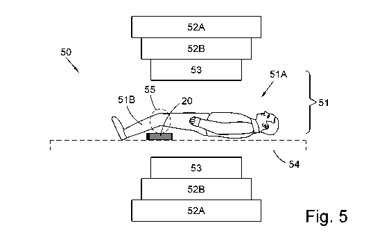
reference to Figure 5.
An MRI system 50 comprises an imaging region 51 arranged to receive an object
to be
imaged, e.g. a human body 51A or human limb 51B. A first coil 52A produces a
static
magnetic field in the imaging region 51 and, in operation, a gradient coil 52B
produces a
gradient to static magnetic field in the imaging region. Together, the first
coil 52A and
gradient coil 52B are a magnetic field generator 52. The system further
comprises an RF
antenna 53 for irradiating the object with an RF signal. The RF antenna 53 is
arranged to
transmit RF signals as a pulse and then have a delay between pulses during
which the
return RF signal is received. The RF antenna 53 may be a RF transmit coil
built into a
housing supporting the first coil and gradient coil, or may be a separate RF
antenna
placed at a location for irradiating the object in the imaging region 51. A
table 54 is located
in the imaging region 51 to support the object to be imaged. The device 20 for
concentrating the magnetic field of RF signals in the MRI system 50 as
described above is
located in the imaging region 51 in proximity of the object, or a particular
target region 55
of the object to be imaged. The device is arranged to concentrate the magnetic
field of RF
signals in the object to imaged. The device is arranged between the RF antenna
53 and
object so, if tuned to the RF signal frequency, the device 20 concentrates the
magnetic
field of the RF signal from the RF antenna 53 to the object in the target
region 55, thereby
.. improving the SN R. As described above, this is by redistributing the
energy between
electric and magnetic fields of the RF signal, increasing the magnetic field
in the target
region 55 and reducing the electric field in the target region 55 which
reduces the SAR.
The RF antenna 53 may also function as an RF receiver, with the return signal
from the
.. object being recorded to image the object. Alternatively, the table 54 may
comprise a
dedicated coil 56 (not shown) which functions as an RF receiver as it receives
the return
signal in order to image the object. In either arrangement, when the device is
positioned
between the object and the RF receiver (tuned to the RF signal), the device 20
will also
concentrate the magnetic field of the return signal as it passes from the
object to the RF
receiver. The system may comprise a plurality of RF antennas 53 to transmit
and/or
receive the RF signals.
17
CA 03169864 2022-08-02
WO 2021/156613 PCT/GB2021/050239
The device 20 may be fixed on, or embedded in, the table 54 or may be a mat
which is
laid on the table 54 prior to introducing the object to be imaged into the
imaging region.
Alternatively, the device may be placed on the object, e.g. in an item of
clothing worn by a
patient.
The device 20 is arranged to resonate with a resonance quality factor and/or
the resonant
RF frequency based on the at least one characteristic of the one or more RF
antenna 53.
Characteristics of the one or more RF antenna may include one or more of: an
RF
frequency that the one or more RF antenna is arranged to transmit; a resonance
quality
factor of the one or more RF antenna; and an object to be imaged by the one or
more RF
antenna, a dielectric constant of the object to be imaged, or a combination
thereof. For
example, the characteristics of the RF antenna 53 may be that it is arranged
to provide RF
radiation at approximately 63.8 MHz, has a resonance quality factor of 100,
and is
arranged to image a patient's head. These are characteristics which can have
an effect on
the resonance performance of the device 20, e.g. the resonant RF frequency or
the
resonance quality factor, as explained below.
In order to produce the beneficial magnetic field manipulation effect, the
device 20 must
resonate at and around the frequency used by the RF antenna 53 to redistribute
energy
between the electric and magnetic fields. The RF antenna frequency influences
the design
of the device 20 and, in particular, a target resonant RF frequency of the
device. Likewise,
the type of object the RF antenna is arranged to image will affect the
resonant RF
frequency of the device, since different objects have dielectric properties
which can shift
the resonance properties of the device when placed near, e.g. during imaging.
For
example, an object with a higher dielectric constant will reduce the resonant
RF frequency
of the device 20 more than a lower dielectric constant object. Hence the
design of the
dielectric material used for the device may be based at least in part on the
object which
the RF antenna is arranged to image.
As another example, if the resonance quality factor is above a threshold
quality factor for
the RF antenna 53, e.g. if the resonance quality factor of the device is
greater than the
resonance quality factor of the RF antenna 53, the resonance effect will
produce
particularly high fields in the imaging region 51 which will disrupt the
performance of the
first coil 52A and/or the gradient coil 52B of the magnetic field generator
52. This can be
caused by the control systems of the magnetic field generator 52 of the MRI
system 50
being programmed to maintain a uniform magnetic field in the imaging region
51. The
presence of a resonating device 20 having a high resonance quality factor
therefore
18
CA 03169864 2022-08-02
WO 2021/156613 PCT/GB2021/050239
disrupts the uniformity of the magnetic field, which may either prompt the
control system
to prevent the MRI system 50 or magnetic field generator 52 from obtaining an
image, or
create an unexpected magnetic field that renders the MRI system unusable for
imaging.
Additionally or alternatively, a high resonance quality factor of the device
20 may detune
the RF antenna, first coil 52A, or gradient coil 52B. The design of the device
may
therefore produce a resonance quality factor of the device 20 in order to not
disrupt the
magnetic field of the MRI system by not detuning the one or more RF antenna 53
or
magnetic field generator 52. This improves the reliability of the device 20
and system 50.
In operation, the MRI system 50 may be used to image an object using the RF
antenna 53
and device 20 as follows. The device 20 is positioned in or adjacent to the
imaging region
51 so to manipulate the magnetic field near the object to be imaged. As an
example, with
reference to figure 5, the device 20 is placed on the table 54 outside the
imaging region
51 of the MRI system at a location where a knee of the human body 51A (i.e.
the patient)
to be imaged will be located. The patient then is positioned on the table 54
with the knee
to be imaged over the device 20 and the table 54, along with the patient and
device 20, is
positioned into the imaging region 51 prior to commencing the imaging process.
Other
examples of body parts the MRI system can be used to image include a wrist, a
spine,
etc. or indeed the MRI system can image an entire body. For the MRI process to
begin, a
static magnetic field is produced in the imaging region, optionally having a
gradient field
according to known MRI techniques.
The MRI system 50 irradiates the device 20 and object with RF radiation as an
RF signal
from the RF antenna 53 and receives a return RF signal from the object to
image the
.. object. The irradiating may comprise transmitting the RF signal as an RF
pulse. The RF
pulse travels to a target region 55 of the object to be imaged via the device
20. If the
device 20 is tuned to the frequency of the RF signal, the device concentrates
the RF
signal in the target region 55 by increasing the magnetic field and reducing
the electric
field. After impinging on the target region 55, the RF signal is emitted from
the target
region 55 as a return RF signal. The return RF signal passes through the
device 20 again
on return to the RF antenna 53 for detection and imaging of the target region
55. The
device may also concentrate the return RF signal by increasing the magnetic
field and
reducing the electric field from the target region 55.
Figure 6 shows a comparison of MRI images produced in an MRI system with and
without
a device 20 as described above. The left image shows an MRI image produced
without a
device 20 for manipulating the magnetic field of RF radiation and the right
image shows
19
CA 03169864 2022-08-02
WO 2021/156613 PCT/GB2021/050239
an MRI image produced with the device 20. The image produced using the device
20 has
improved contrast in the target region 55 of the object, in this case, part of
the patient's
foot and ankle. This is due to the increased magnetic field in the target
region of the
object.
Methods of producing the device
With reference to Figure 7, a method 700 of producing a device for
manipulating a
magnetic field of RF radiation from one or more RF antenna in an MR system
comprises:
determining 702 a target resonance quality factor and/or a target resonant RF
frequency
of the device; determining 704 a design of the device to provide the device
with the
determined target resonance quality factor and/or target resonant RF frequency
of the
device; and making 706 the device in accordance with the design. The device to
be
produced can be any device as described above for use in an MR system as
described
above.
The determining 702 a target resonance quality factor and/or a target resonant
RF
frequency of the device is based on at least one characteristic of the one or
more RF
antenna of the MR system, such as an MRI system as described above with
reference to
Figure 5.
As an example, a target resonance quality factor of the device is based on a
resonance
quality factor of an RF antenna of an MRI system, i.e. the resonance quality
factor of the
RF antenna is the characteristic, as explained below.
A user input is received at a processor, the user input defining a resonance
quality factor
of a RF antenna of the MR system which is a characteristic of the RF antenna.
The user
input is received at a user interface associated with the processor. The user
input may
provide the characterisitc of the RF antenna by including a numerical value,
or a
numerical range, of the resonance quality factor of the RF antenna, e.g.
specifies a
resonance quality factor of 90, or between 50 and 100, or between 80 and 100.
The
processor then determines the target resonance quality factor of the device to
be
produced based on the value of the the resonance quality factor of the RF
antenna
provided by the user input. For example, this is done by using a target
criterion such as
the target resonance quality factor of the device is determined to be less
than the
resonance quality factor of the RF antenna. Alternative criteria include: that
the target
resonance quality factor of the device is determined to be below a certain
percentage of
the resonance quality factor of the RF antenna; or that the target resonance
quality factor
CA 03169864 2022-08-02
WO 2021/156613 PCT/GB2021/050239
of the device is determined to be approximately a certain percentage of the
resonance
quality factor of the RF antenna, e.g. approximately 80% of the value of the
resonance
quality factor of the RF antenna.
The criterion or criteria to determine the target resonance quality factor of
the device may
be such that that the device does not detune the one or more RF antenna when
used in
the MR system. This is to avoid the phenomenon, as described above with
reference to
Figure 5, of the device 20 for manipulating a magnetic field of RF radiation
from disrupting
the performance of the RF antenna 53 or the magnetic field generator 52 of the
MRI
system 50. Accordingly, determining the target resonance quality factor of the
device
based on the characteristic of the RF antenna, namely a resonance quality
factor,
improves the reliability of the device to be produced.
Other characteristics of the RF antenna that the target resonance quality
factor of the
device is based on include an RF frequency that the RF antenna is arranged to
transmit;
the dimensions of the RF anteanna; the power source used to power the RF
antenna; an
object to be imaged by the RF antenna; a loss tangent of the object to be
imaged by the
RF antenna; and a dielectric contstant of the obejct to be imaged by the RF
antenna; or
any other characterisitic which can affect the interactions between the device
20 to be
produced and the RF antenna 53 of the MRI system 50.
As another example of the determining 702 in Figure 7, the target resonant RF
frequency
of the device is determined based on an RF frequency that the RF antenna 53 is
arranged
to transmit. i.e. the resonant RF frequency of the RF antenna is the
characteristic, as
explained below.
The resonant RF frequency of the RF antenna is received at the processor in a
user input,
similar to as described in the previous example, except that the user input
comprises a
numerical value or range for the resonant RF frequency that the RF antenna is
arranged
to transmit. For example, the value or range may be that the RF antenna 53 is
arranged to
transmit at 63.8 MHz, or between 60 MHz and 65 MHz. The processor stores the
received
numerical value or numerical range from the user input as the target resonant
RF
frequency. The processor then determines the target resonant RF frequency the
device to
be produced based on the value or range of the RF frequency of the RF antenna
provided
by the user input. For example, the processor may store the received numerical
value or
numerical range from the user input as the target resonant RF frequency. This
is so that
the device 20 to be produced will provide the effect of manipulating the
magnetic field of
21
CA 03169864 2022-08-02
WO 2021/156613 PCT/GB2021/050239
the RF radiation from the RF antenna, i.e. by resonating at the frequency that
the RF
antenna transmits. The target resonant RF frequency may be the range between
95% and
105% of the RF frequency of the RF antenna. Alternatively, the processor may
apply a
criteria or calculation to determine the target resonant RF frequency for the
device. For
example, the target resonant RF frequency may be 95% of the value of the RF
frequency
of the RF antenna, or 105% of the value of the RF frequency of the RF antenna.
This may
be done to control the resonance strength of the device 20.
Other characteristics of the RF antenna that the target resonant RF frequency
of the
device is based on include: a resonance quality factor of the the RF antenna;
the
dimensions of the RF antenna; the power source used to power the RF antenna;
an object
to be imaged by the RF antenna; a loss tangent of the object to be imaged by
the RF
antenna; a dielectric contstant of the object to be imaged by the RF antenna;
and/or any
other characterisitic which can affect the interactions between the device 20
to be
produced and the RF antenna 53 of the MRI system 50. For example, the a
resonance
quality factor of the the RF antenna, which is related to the frequency width
of the RF
antenna frequency peak, may influence how close the target resonant RF
frequency
should be to the RF frequency of the RF antenna. The type of object that the
RF antenna
is arranged to image, or the loss tangeant and/or dielectric constant of the
object, will
affect the level of detuning of the device resonant RF frequency when the
object is placed
in proximity with the device 20 during imaging. Hence the target resonant RF
frequency
can be determined to based on these parameters of the object to be imaged by
the RF
antenna in order to provide the desirable resonance characteristics of the
device 20 in
use, thereby improving the performance of the device. For example, if the RF
antenna 53
is for imaging a high dielectric constant object, the target resonant RF
frequency can be
determined to be higher than the RF frequency of the RF antenna 53 in
accordance with
equation 1. Therefore, when used with the object, the decrease in resonant RF
frequency
of the device caused by the object will re-tune the device 20 to the RF
frequency of the RF
antenna 53.
In either of the above examples of determining 702, the determined target
resonance
quality factor and/or the determined target resonant RF frequency may be a
range of
values.
As part of the determining 702, the processor may receive an RF antenna
identifier
associated with the RF antenna 53 the device is to be used with. The RF
antenna
identifier is associated with further characteristics of the RF antenna stored
in a memory,
22
CA 03169864 2022-08-02
WO 2021/156613 PCT/GB2021/050239
e.g. as part of a look-up table. The determining 702 may comprise the
processor retrieving
characteristics of the RF antenna from the memory using the RF antenna
identifier and
using the retrieved characterisitcs to base the determining of target
resonance quality
factor on.
As part of the determining 702, the processor may measure the characteristics
of the RF
antenna 53, e.g. using an electromagentic field sensor arranged to receive RF
radiation
from the RF antenna. The measuring may also comprising controlling an input to
the RF
antenna to measure performance over a range of frequencies.
As part of the determining 702, the processor may include calculating the
target
resonance quality factor and/or target resonant RF frequency using an equation
based on
the at least one characteristic of the one or more RF antenna.
As an alternative to using predetermined criteria for determining 702 the
target resonance
quality factor and/or target resonant RF frequency, simulation can be used.
For example,
the characteristics of the RF antenna 53 are input into a simulation, e.g. a
Finite-difference
time-domain (FDTD) simulation, along with trial values for the target
resonance quality
factor and/or target resonant RF frequency. The RF antenna 53 and a device 20
having
the trial values are simulated and the results of the simulation show the
performance of
the device, which can be assessed to determine whether or not the trial values
should
become the target value for the device to be produced. The assessment may be
based on
any particular desired outcome but, as an example, this may be that RF antenna
53
produces resonance in the device 20 and the device 20 does not detune any of
the other
components. The magnetic field generator 52 and object to be imaged may also
be
included in the simulation.
In some examples, the system in which the device 20 is arranged to be used has
a
plurality of RF antennas. In these examples the determining 702 a target
resonance
quality factor and/or target resonant RF frequency of the device can be based
on one of
the plurality of RF antennas, or on two or more of the RF antennas. For
example, the
target resonance quality factor may be determined to be less than the lowest
value of
each of the resonance quality factors of the RF antennas, or to be less than
an average
value of the resonance quality factors of the RF antennas. The determining 702
a target
resonant RF frequency of the device 20 can be based on an average of the
resonant RF
frequencies of the RF antennas, or based on an average dielectric constant of
the one or
23
CA 03169864 2022-08-02
WO 2021/156613 PCT/GB2021/050239
more objects to be imaged by the respective RF antennas, or any other criteria
for
optimising performance of the system for which the device 20 is arranged to be
used with.
With reference to Figure 7, the determining 704 the design of the device is to
provide the
device with the determined target resonance quality factor and/or target
resonant RF
frequency of the device, as determined using any of the approaches described
above.
As discussed above, with reference to Figure 2 when describing devices for
manipulating
a magnetic field, the design of the device 20, in general, includes one or
more parameters
which affect the resonance quality factor and/or resonant RF frequency of a
device made
according to the design. For example, the design may define one or more of:
the dielectric
permittivity of the dielectric material; the loss tangent of the dielectric
material 26; one or
more electronic components connected between two respective portions of the
conductive
elements 22; a length of the conductive elements 22; a proportion of the
length of the
conductive elements 22 along which the dielectric material 26 is positioned;
the
composition of the dielectric material 26, or any parameter which affects the
resonant
properties of the device 20. Optionally, the design may also include further
properties of
the device 20 to be made, such as: the materials of the conductive elements
22, the
dimensions of the device, the presence and size of any spacers 42 to be used,
etc. Any
features of the device to be made not specified by the design may be given a
default
value, or may be specified using additional user inputs.
As an example, the determining 704 the design in order to provide the
determined 702
target resonance quality factor includes determining the loss tangent of the
dielectric
material 26 of the device 20 to be produced. This may be done by the processor
retrieving
from a memory a value of loss tangent of the dielectric material to provide
the target
resonance quality factor, or if the target resonance quality factor is a
range, a value within
the range. Alternatively, the loss tangent may be calculated using an equation
relating
loss tangent to resonance quality factor of the device, e.g. an equation
derived empirically
from measurements of devices having different loss tangents. Alternatively,
the processor
may perform a simulation, e.g. a FDTD simulation, with a trial loss tangent
value and
default values for any other relevant parameters of the device 20 and input RF
radiation.
The resonance quality factor of the simulated device can be calculated using
equation 2. If
the resonance quality factor the simulated device provides the determined 702
target
resonance quality factor, then the design of the device 20 is determined to
include the trial
loss tangent. If the resonance quality factor of the simulated device does not
provide the
determined 702 target resonance quality then a different trial loss tangent is
used in a
24
CA 03169864 2022-08-02
WO 2021/156613 PCT/GB2021/050239
further simulation until a value is found which provides the target resonance
quality factor,
which will then be used for the design of the device 20. Optionally,
determining the design
may also include selecting a material to use for the dielectric material 26
which has the
determined loss tangent of the design. Another alternative is to make a trial
device having
the trial loss tangent and measuring the resonance quality factor of the trial
device using
input radiation and sensors to detect the resonance properties of the trial
device.
If the design of the device includes multiple parameters affecting the
resonance quality
factor of the device 20, then these parameters may all be determined, either
one-by-one
or collectively, using the above methods. For example, all of the parameters
can be
simulated until a design to produce the target resonance quality factor is
determined.
Alternatively, the processor may retrieve sets of values from the memory,
which produce
the target resonance quality factor when used in the design.
As another example, the determining 704 the design in order to provide the
determined
702 target resonant RF frequency includes determining the positioning of the
dielectric
material 26, e.g. the proportion of the length of the conductive elements 22
along which
the dielectric material 26 is located. As described above for determining a
design to
provide a target resonance quality factor, determining the design to provide a
target
resonant RF frequency may be done by calculation, retrieval from memory,
simulation or
measurement using a similar process to as previously described. For example,
equation 1
can be used to calculate the proportion of the length of the conductive
elements 22 along
which the dielectric material. In particular, the relative dielectric
permittivity c of the
environment that the conductive elements are in can be approximated by:
E P Ed + (1 ¨ MEd (4)
where P is the proportion of the length of the conductive elements 22 along
which the
dielectric material 26 is located (0< P < 1), cd is the relative dielectric
permittivity of the
dielectric material 26 and c, is the dielectric material of air (or whatever
substance
surrounds the portion of the conductive elements where the dielectric material
is not
located). For example, using equations 1 and 4, to provide a device with
resonant RF
frequency of 62 MHz, with conductive elements having length of 50cm,
dielectric material
relative dielectric permittivity of 75, the required proportion of the length
of the conductive
elements 22 along which the dielectric material 26 is located is approximately
0.3, or 30%,
e.g. 15% of the length at each end of the conductive elements. This is because
the
CA 03169864 2022-08-02
WO 2021/156613 PCT/GB2021/050239
effective relative dielectric permittivity is 23.2 = (0.3*75) + (0.7*1) using
equation 4 and the
resonant RF frequency using equation 1 is 62.3 MHz = c / (2*0.5*\/23.2).
Alternatively or
additionally, the dielectric permittivity of the dielectric material and/or
the length of the
conductive elements can be determined for the design using the equations 1
and/or 4.
If the design of the device includes multiple parameters affecting the
resonant RF
frequency of the device 20, then these parameters may all be determined,
either one-by-
one or collectively, using the above methods. For example, all of the
parameters can be
simulated until a design to produce the target resonant RF frequency is
determined.
Alternatively, the processor may retrieve sets of values from the memory,
which produce
the target resonant RF frequency when used in the design. If the design of
device is to
produce both a target resonance quality factor and a target resonant RF
frequency, then
further parameters affecting either or both the resonant RF frequency and
resonance
quality factor are calculated or simulated together to provide the target
resonance
properties.
With reference to Figure 7, the determining 706 the making the device in
accordance with
the design may include assembling the conductive elements 22, dielectric
material 26 into
a device 20 as described with reference to Figures 1 to 4.
As an example, the making 706 may include fabricating one or more PCBs 21
having
metal strips 22 of either a predetermined length or, if specified in the
design, with a length
according to the design of device. Alternatively, the PCBs 21 may have been
fabricated
prior to the making 706 of the device. The PCBs can be made using conventional
PCB
fabrication techniques.
If the design of the device includes one or more electronic components
connected
between two respective portions of the conductive elements, e.g. metal strips
22, these
may be built in to the PCBs during the fabrication process, or connected
between the
relevant conductive elements according to the design in a second process after
the PCB
has been fabricated. Either a controller of the electronic components, or an
electrical input
port to receive a control signal for the electronic components, is also
included in the
device. A power source, e.g. a battery, or a power connection, e.g. a power
port, to power
the controller and/or electronic components may also be included. For example,
a
potentiometer and DC power source as described with reference to Figure 3 may
be
included in the device.
26
CA 03169864 2022-08-02
WO 2021/156613 PCT/GB2021/050239
The PCBs 21 are stacked with the dielectric material 26 positioned above and
below each
PCB 21, located at end portions of the lengths of the metal strips 22. Ceramic
blocks 27
may be used for the dielectric material 26, either prefabricated or by
selecting the material
for the ceramic block, e.g. BaTiO3 or CaTiO3, and forming the material into
the ceramic
blocks 27. If the device to be produced is a composite device 40 as described
above with
reference to Figures 4A to 4C, the making 706 comprises positioning the two or
more
component devices 20 on either side of the one or more spacers 42.
The stack of PCBs 21 and ceramic blocks 27, and optionally spacers between
component
devices 20, may be held together using adhesives or mechanical fasteners such
as
screws or bolts. Alternatively, the items of the stack are positioned in a
housing to hold the
items in position with respect to each other. This may be done by the housing
having a
plurality of slots in which the items can be slid into.
If the device is arranged to have moving parts, such as a slidable dielectric
material 26,
these parts are attached to the rest of the device using a sliding mechanism.
Hence the
device is an adjustable device. In an example, the ceramic blocks 27 are
coupled to the
housing using wheels and axles attached to each ceramic block 27 arranged to
engage
with slots or runners in the housing. The ceramic blocks may include a handle,
connected
to one or more ceramic block either individually or collectively, so that a
user can manually
change the positioning of the ceramic blocks 27 along the slots or runners.
Alternatively,
an actuator is coupled to one or more of the ceramic blocks 27 to control the
positioning of
the ceramic blocks.
In an example of a method 700 of producing a device 20 for manipulating a
magnetic field
of RF radiation from one or more RF antenna 53 in an MR system 50, an
adjustable
device is already assembled prior to the determining of a target resonance
quality factor
and/or target resonant RF frequency of the device. The making 706 of the
device 20 in
accordance of the design comprises adjusting one or more parameters of the
adjustable
device in order to provide the device with the determined target resonance
quality factor
and/or determined target resonant RF frequency of the device 20.
For example, the method 700 may be performed during imaging of an object by an
MRI
system 50. The determining 702 of a target resonant RF frequency of the device
may be
based on measurement of the RF frequency transmitted by the RF antenna 53, or
based
on the dielectric properties of the object 51 into which the RF antenna 53 is
transmitting
(or any of the other examples provided above for determining 702). This may be
27
CA 03169864 2022-08-02
WO 2021/156613 PCT/GB2021/050239
performed in accordance with any of the methods previously described, or may
include
determining if the adjustable device resonant RF frequency is too low or too
high
compared to the RF frequency of the RF antenna. Hence the target resonant RF
frequency may be to adjust the device to make the device either increase or
decrease its
resonant RF frequency.
A processor, either part of the device 20 or otherwise arranged to control the
device 20,
determines 704 a design of the device in order to provide the determined
target resonant
RF frequency of the device. For example, to produce a device 20 with a higher
resonant
RF frequency, the design has the dielectric material positioned along a
smaller proportion
of the conductive elements than the starting proportion (in accordance with
equations 1
and 4). In other words, to make 706 the device 20 in accordance with the
determined 704
design, the adjustable device should be adjusted to slide the dielectric
material 26 away
from the conductive elements so less of each conductive element is covered. On
the other
hand, to produce a device 20 with a lower resonant RF frequency of the device,
the
adjustable device should be adjusted to slide the dielectric material to cover
a greater
proportion of the conductive elements.
Alternatively, if the proportion of the conductive elements covered by the
dielectric
component does not change, e.g. in terms of Figure 2 because the ceramic
blocks 27
have been slid so that their entire width covers the metal strips 22, then the
location of
dielectric material along the length of the conductive elements also has an
effect of the
resonant RF frequency. In an example, the dielectric material comprises two
blocks at
either end of the conductive elements. As the blocks are moved in from the
ends of the
conductive element, the proportion of the conductive elements that they cover
increases
and the RF resonant frequency decreases, as explained above. Once the entire
width of
the dielectric material blocks covers the conductive elements, moving the
blocks further
towards the midpoint of the conductive elements no longer increases the
proportion of the
conductive elements covered and the effective permittivity of the surroundings
remains
substantially constant. However, as the blocks continue to move closer to the
midpoint of
the conductive elements, this has a different effect of decreasing the
effective length of
the conductive elements, thereby increasing the resonant RF frequency. The
particular
effect of the positioning of the dielectric material on the resonant RF
frequency can be
determined empirically or by simulation, as explained above.
To make 706 the device in accordance with the design, the processor sends
instructions
to the actuator to adjust the proportion of the conductive elements along
which the
28
CA 03169864 2022-08-02
WO 2021/156613 PCT/GB2021/050239
dielectric material 26 is located in accordance with the determined design.
Alternatively,
the processor may provide an output at a user interface indicating the
adjustment of the
dielectric material required for a user to manually adjust the proportion of
the conductive
elements along which the dielectric material 26 is located in accordance with
the
determined design. The user then adjusts the proportion of the conductive
elements along
which the dielectric material 26 is located using the handle and sliding
mechanism of the
adjustable device.
The method 700 of producing the device 20 may use an adjustable device having
adjustable parameters other than proportion of the conductive elements along
which the
dielectric material is located. For example, the length of conductive elements
may be
adjustable by providing extensions arranged next to each conductive elements
with a
respective switch or electronic component to connect or disconnect each
extension from
the respective conductive element, to adjust the effective length of the
conductive
elements. Alternatively, electronic components connected between two
respective
portions of the conductive elements, as described with reference to Figure 3,
can be
controlled to adjust the loss of the device and thereby changing the resonance
quality
factor of the device. In any of the above examples, the making 706 of the
device 20 in
accordance with the deign includes adjusting a parameter of the device in
order to meet
the design, to produce the target resonance properties.
One or more of the features of the method 700 may be computer-implemented,
e.g.
performed by a processor. For example, the determining 702 a target resonance
quality
factor and/or a target resonant RF frequency of the device based on at least
one
characteristic of the one or more RF antenna, and/or the determining 704 a
design of the
device to provide the device with the determined target resonance quality
factor and/or the
target resonant RF frequency of the device may be computer-implemented by a
processor. The making 706 the device in accordance with the design may include
the
processor instructing a making apparatus to make the device in accordance with
the
determined design.
The methods described above may be implemented by a computer program product.
The
computer program product may include computer code arranged to instruct a
computer to
perform part of the functions of one or more of the methods described above.
The
computer program and/or the code for performing such methods may be provided
to an
apparatus, such as a computer, on a computer readable medium or computer
program
product. The computer readable medium may be transitory or non-transitory. The
29
CA 03169864 2022-08-02
WO 2021/156613 PCT/GB2021/050239
computer readable medium could be, for example, an electronic, magnetic,
optical,
electromagnetic, infrared, or semiconductor system, or a propagation medium
for data
transmission, for example for downloading the code over the internet.
Alternatively, the
computer readable medium could take the form of a physical computer readable
medium
such as semiconductor or solid-state memory, magnetic tape, a removable
computer
diskette, a random access memory (RAM), a read-only memory (ROM), a rigid
magnetic
disc, and an optical disk, such as a CD-ROM, CD-R/VV or DVD.
A computer apparatus such as a computer may be configured in accordance with
such
code to perform one or more processes in accordance with the methods discussed
herein,
in combination with an apparatus for making 706 a device 20 in accordance with
the
design. Such a computer apparatus may take the form of a data processing
system. Such
a data processing system may be a distributed system. For example, such a data
processing system may be distributed across a network.
In an implementation, the modules, components and other features described
herein can
be implemented as discrete components or integrated in the functionality of
hardware
components such as ASICS, FPGAs, DSPs or similar devices.
A "hardware component" is a tangible (e.g., non-transitory) physical component
(e.g., a
set of one or more processors) capable of performing certain operations and
may be
configured or arranged in a certain physical manner. A hardware component may
include
dedicated circuitry or logic that is permanently configured to perform certain
operations. A
hardware component may be or include a special-purpose processor, such as a
field
programmable gate array (FPGA) or an ASIC. A hardware component may also
include
programmable logic or circuitry that is temporarily configured by software to
perform
certain operations.
Accordingly, the phrase "hardware component" should be understood to encompass
a
tangible entity that may be physically constructed, permanently configured
(e.g.,
hardwired), or temporarily configured (e.g., programmed) to operate in a
certain manner
or to perform certain operations described herein.
In addition, the modules and components can be implemented as firmware or
functional
circuitry within hardware devices. Further, the modules and components can be
implemented in any combination of hardware devices and software components, or
only in
CA 03169864 2022-08-02
WO 2021/156613 PCT/GB2021/050239
software (e.g., code stored or otherwise embodied in a machine-readable medium
or in a
transmission medium).
Kit
With reference to Figure 8, a kit 800 comprises at least one RF antenna 53 and
a device
20 for manipulating a magnetic field of RF signals in an MR system. The device
20 is
arranged to resonate with a resonance quality factor and/or a resonant RF
frequency
based on at least one characteristic of the at least one RF antenna. The RF
antenna 53
device 20 may have any of the features or properties discussed above. The kit
may also
comprise a plurality of RF antennas 53, which the properties of the device
being based on
the one or more characteristics of the plurality of RF antennas as described
above.
The device 20 of the kit 800 is the product of any of the methods 800 of
producing the
device for manipulating a magnetic field of RF radiation from one or more RF
antenna in
an MR system as described above. In particular, the device 20 is made in
accordance
with a design which provides the device with a target resonance quality factor
and/or
target resonant RF frequency of the device, which are determined based on at
least one
characteristic of the RF antenna 53. Hence the device 20 and RF antenna 53 are
configured with complementary properties to provide improved performance of an
MRI
system using the kit 800.
The kit may further include the computer program product as describe above.
It is to be understood that the above description is intended to be
illustrative, and not
restrictive. Many other implementations will be apparent to those of skill in
the art upon
reading and understanding the above description. Although the present
disclosure has
been described with reference to specific example implementations, it will be
recognized
that the disclosure is not limited to the implementations described but can be
practised
with modification and alteration within the scope of the appended claims.
Accordingly, the
.. specification and drawings are to be regarded in an illustrative sense
rather than a
restrictive sense. Although various features of the approach of the present
disclosure
have been presented separately (e.g., in separate figures), the skilled person
will
understand that, unless they are presented as mutually exclusive, they may
each be
combined with any other feature or combination of features of the present
disclosure.
31