Note: Descriptions are shown in the official language in which they were submitted.
CA 03169875 2022-08-02
WO 2021/240515
PCT/1L2021/050610
METHOD OF FABRICATION OF COMPOUND LIGHT-GUIDE OPTICAL
ELEMENTS
FIELD AND BACKGROUND OF THE INVENTION
The present invention relates to light-guide optical elements (LOE), and, in
particular,
to compound LOEs for two-dimensional image expansion and their methods of
manufacture.
Compound LOEs or "two-dimensional expansion waveguides" have been described in
previous publications by Lumus Ltd. (Israel). Examples of such compound LOEs
may be
found, for example, in PCT publication WO 2020/049542. In general terms, these
compound
LOEs employ two regions, each of which is a parallel-faced block of
transparent material for
supporting propagation of light carrying a collimated image by internal
reflection at major
surfaces, and includes a set of mutually-parallel, internal, partially-
reflecting surfaces or
"facets", which redirect the collimated image while achieving expansion of the
optical
aperture. By combining two such elements with different facet orientations, it
is possible to
achieve two-dimensional expansion of an optical aperture within a single
element, thereby
expanding an input image from an image projector and outputting it over a
larger area towards
the eye of an observer.
SUMMARY OF THE INVENTION
According to one aspect of the present invention there is provided a method of
fabricating a compound light-guide optical element (LOE), including: providing
a bonded stack
of a plurality of LOE precursors and a plurality of transparent spacer plates,
the stack having a
first pair of parallel faces, the stack including alternating LOE precursor
and transparent spacer
plates along a length of the stack perpendicular to the pair of parallel
faces, each LOE
precursor comprising a pair of major parallel surfaces and a first plurality
of mutually parallel
partially reflective internal surfaces angled obliquely relative to the pair
of parallel surfaces;
providing a first optical block having a second pair of parallel faces, and a
plurality of mutually
parallel internal surfaces angled obliquely relative to the second pair of
parallel faces, the
internal surfaces being at least partly partially reflective such that the
first block includes a
second plurality of mutually parallel partially reflective internal surfaces;
bonding the first
block to the stack such that one of the faces of the first block is joined to
one of the faces of the
stack and the first plurality of partially reflective internal surfaces is non-
parallel to the second
plurality of partially reflective internal surfaces, thereby forming a second
optical block; and
1
CA 03169875 2022-08-02
WO 2021/240515
PCT/1L2021/050610
slicing out at least one compound LOE from the second block by cutting the
second block
through at least two consecutive spacer plates having a LOE precursor
sandwiched
therebetween.
According to some aspects, the internal surfaces of the first block are each
only partly
coated with a partially reflective coating, such that internal surface
comprises strips of partially
reflective coating with gaps therebetween.
According to some aspects, the method includes polishing the face of the stack
that will
be joined to the first block prior to bonding the stack with the first block
and/or polishing the
face of the first block that will be joined to the stack prior to bonding the
first block with the
stack.
According to some aspects, the method includes, prior to bonding the first
block to the
stack: aligning the first block and the stack such that first plurality of
partially reflective
internal surfaces and the second plurality of partially reflective internal
surfaces are orthogonal.
According to some aspects, the method includes polishing the external surfaces
of the
sliced-out at least one compound LOE that are parallel to the major parallel
surfaces of the
LOE precursor.
According to some aspects, the internal surfaces of the first block are each
only partly
coated with a partially reflective coating, such that internal surface
comprises strips of partially
reflective coating with gaps therebetween.
According to another aspect of the present invention there is provided an
optical
structure that is an intermediate work product of a compound LOE fabrication
process, the
optical structure including: a first region including a plurality of LOE
precursors separated by
transparent spacer plates therebetween, each LOE precursor including a pair of
major external
parallel surfaces and a first plurality of mutually parallel partially
reflective internal surfaces
being angled obliquely relative to the pair of parallel surfaces; a second
region including a
second plurality of mutually parallel partially reflective internal surfaces
being non-parallel to
the first plurality of partially reflective surfaces; and at least one
internal surface separating the
first and second region, the internal surface being perpendicular to the pairs
of parallel
surfaces.
According to some aspects, the optical structure is formed by bonding a first
optical
block including the first region with a second optical block including the
second region.
2
CA 03169875 2022-08-02
WO 2021/240515
PCT/1L2021/050610
According to some aspects, the optical structure can include a third optical
region
between the first region and the second region. The third optical region can
include one or
more optical elements. The optical elements can be optically active elements
or optically inert
elements. In some aspects, at least one sub-region within the second region
can be free of any
partially reflective internal surfaces and/or each LOE precursor in the first
region can include at
least one sub-region that is free of any partially reflective internal
surfaces.
BRIEF DESCRIPTION OF THE DRAWINGS
The invention is herein described, by way of example only, with reference to
the
accompanying drawings, wherein:
FIGS. 1(a) ¨ 1(b) illustrate an embodiment of a compound LOE according to the
prior art;
FIGS. 2(a) ¨ 2(c) illustrate known methods of fabricating a compound LOE;
FIGS. 3(a) ¨ 3(b) illustrate another embodiment of a compound LOE;
FIGS. 4(a) ¨ 4(b) illustrate an LOE having a given thickness dl;
FIGS. 5(a) ¨ 5(b) illustrate a stack of bonded LOE precursors separated by
transparent
plates of a given thickness d2;
FIGS. 6(a) ¨ 6(b) illustrate a block of transparent plates;
FIG. 6(c) illustrates a method of forming the block of FIGS. 6(a) ¨ 6(b);
FIGS. 7(a) ¨ 7(b) illustrate an optical structure formed from bonding the
block of FIGS.
6(a) ¨ 6(b) to the stack of FIGS. 5(a) ¨ 5(b);
FIGS. 7(c) ¨ 7(d) illustrate a slice taken from the block of FIGS. 7(a) ¨
7(b);
FIGS. 8(a) ¨ 8(b) illustrate an alternative embodiment of the block of FIGS.
6(a) ¨ 6(b);
FIGS. 9(a) ¨ 9(b) illustrate an optical structure foimed from bonding of the
block of FIGS.
8(a) ¨ 8(b) with the stack of FIGS. 5(a) ¨ 5(b);
FIGS. 10(a) ¨ 10(b) illustrate a compound LOE cut from the optical structure
of FIGS.
9(a) ¨ 9(b);
FIGS. 11(a) ¨ 11(b) illustrate another embodiment of block 16;
FIGS. 12(a) ¨ (b) illustrate an optical structure formed from bonding of the
block of FIGS.
11(a) ¨ 11(b) with the stack of FIGS. 5(a) ¨ 5(b);
FIGS. 12(c) ¨ (d) illustrate a slice taken from the optical structure of FIGS.
12(a) ¨ (b);
FIGS. 13(a) ¨ 13(b) illustrate another embodiment of block 16; and
FIGS. 13(c) ¨ (d) illustrate a slice taken from the optical structure of FIGS.
13(a) ¨ (b).
3
CA 03169875 2022-08-02
WO 2021/240515
PCT/1L2021/050610
DESCRIPTION OF THE PREFERRED EMBODIMENTS
FIGS. 1(a) ¨ 1(b) illustrate an embodiment of a compound LOE 100 according to
the
prior art. Compound LOE 100 includes a first LOE 1 and a second LOE 2 bonded
together at
interface 102. LOE 1 includes a pair of major parallel surfaces 101, 102 and a
plurality of
mutually parallel partially reflective internal surfaces ("facets") 4 that are
obliquely angled
relative to surfaces 101, 102. The reflectivity is provided via coatings on
the internal surfaces
prior to forming LOE 1. The reflectance of each of the facets may be the same
or different
from one another. Facets 4 are configured to guide an image from an external
micro- projector
(not shown) towards LOE 2 while expanding the image in one dimension (in this
case the x-
dimension). LOE 1 includes surfaces 103 that are perpendicular to surfaces
101, 102.
LOE 2 also include a pair of major parallel surfaces 201 that are
perpendicular to
surfaces 101, 102 of LOE 1, and a plurality of mutually parallel partially
reflective facets 5 that
are obliquely angled relative to surfaces 201. In some embodiments, as shown
in FIGS. 1(a) ¨
1(b), the spatial orientation of facets 5 relative to facets 4 may be
orthogonal, although other
orientations are also possible depending on the design specifications of the
specific application
for the compound LOE. The reflectivity of facets 5 is provided via coatings on
the internal
surfaces prior to forming LOE 2. The reflectance of each of facets may be the
same or
different from one another. Facets 5 are configured to guide the image from
LOE 1 (now
expanded in one dimension) to an observer while expanding the image in the
second dimension
(in this case the z-dimension)
Compound LOE 100 further includes transparent cover plates 3 on the surfaces
of LOE
100 in the XZ plane. The surfaces covered by plates 3 include surfaces 103 of
LOE 1 and
surfaces 201 of LOE 2. Accordingly, these surfaces need to be accurately
aligned in order to
apply plates 3.
FIGS. 2(a) ¨ 2(c) illustrate known methods of fabricating a compound LOE.
Typically, LOE 1 and LOE 2 are manufactured separately and bonded together.
Throughout
this document, the term "bonding" should be understood to mean attaching with
an optical glue
or adhesive. The bonded LOEs are then polished on the external surfaces. Cover
plates 3 are
applied to the polished surfaces, and these cover plates are then typically
polished as well.
Using this fabrication method, the bonding process between LOE 1 to LOE 2 must
be
performed with very high precision so that surfaces 103 of LOE 1 are in the
same plane as the
corresponding surfaces 201 of LOE 2. This method is prone to misalignment as
shown in
FIGS. 2(a) ¨ 2(c).
4
CA 03169875 2022-08-02
WO 2021/240515
PCT/1L2021/050610
In order to overcome the difficulties described above, the present invention
discloses a
new method of fabricating a compound LOE. In addition to overcoming the
problems of
precise alignment during bonding of LOE 1 to LOE 2, the presently disclosed
process allows
for fabrication of a new embodiment of compound LOE 100 in which transparent
cover plates
3' exist only on surfaces 201 of LOE 2, as shown in FIGS. 3(a) ¨ 3(b). This
embodiment of
the compound LOE is discussed in further detail in a co-pending PCT
application entitled
"Compound Light-Guide Optical Elements", filed on the same day as this
application, taking
priority from US provisional patent application no. 63/029,496 that was filed
24 May 2020.
FIGS. 4(a) ¨ 4(b) illustrate a LOE "precursor" 2', which should be understood
to
mean an intermediate optical element in the production of LOE 2. LOE precursor
2' includes a
pair of major parallel external surfaces 6 and a plurality of mutually
parallel partially reflective
internal surfaces ("facets") 5 angled obliquely relative to the pair of
parallel surfaces. The
LOE precursor has a predetermined thickness between surfaces 6 which is
denoted herein as
dl. Known methods exist for manufacturing a LOE precursor, for example as
described in
PCT Publication WO 2016/103263.
Referring now to FIGS. 5(a) ¨ 5(b), after fabricating a plurality of LOE
precursors, a
bonded stack 15 of the plurality of LOE precursors having the same thickness
di and a
plurality of transparent spacer plates 7 is formed. The stack is composed of
alternating LOE
precursor and transparent spacer plate along the length of the stack (y-
dimension). Each
transparent plate has the same predetermined thickness denoted herein as d2.
Stack 15 has a
pair of parallel faces 8a, 8b extending along the length of the stack
perpendicular to surfaces 6.
Referring now to FIGS. 6(a) ¨ 6(b), an optical block 16 with parallel faces
10a, 10b is
formed from a plurality of bonded, transparent coated plates 17 (each plate
coated with a
partially reflective coating), thereby forming a plurality of mutually
parallel partially reflective
internal surfaces 9 that are each angled obliquely relative to face 10b at a
predetermined angle
11 (also referred to as the "facet tilt angle").
Known methods exist for forming optical block 16. For example, as shown in
FIG.
6(c), one method includes stacking and bonding a plurality of coated plates 17
and cutting the
stack along the dashed lines shown in FIG. 6(c), in order to extract the
block. Face 10b is then
polished by a polishing apparatus 18 to achieve the desired facet tilt angle
11, which may vary
according to the particular design specifications of the final compound LOE.
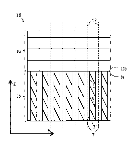
Referring now to FIGS. 7(a) ¨ 7(b), block 16 is aligned with and bonded to
stack 15
thereby forming an optical block 18. More specifically, face 10b of block 16
is bonded to face
5
CA 03169875 2022-08-02
WO 2021/240515
PCT/1L2021/050610
8a of stack 15. Either or both of face 10b and 8a may be polished flat prior
to bonding. The
particular alignment between block 16 and stack may vary according to the
design
specifications of the product. In the embodiment corresponding to the compound
LOE shown
in FIGS. 3(a) ¨ 3(b), the alignment of the blocks 15 and 16 can be understood
as follows, with
reference to the coordinate system XYZ shown in FIGS. 7(a) ¨ 7(b). Stack 15
and block 16
shall be aligned so that surfaces 6 of LOE precursors 2' are parallel to the
plane XZ, face 8a of
stack 15 is parallel to the plane XY, facets 5 of the LOE precursors 2' are
perpendicular to the
plane YZ, plates 17 of block 16 are perpendicular to the plane XZ, and face
10b of block 16 is
parallel to the plane XY. After alignment, plates 17 are perpendicular to the
surfaces 6 of LOE
precursors 2' in stack 15.
The aligned and bonded structure is denoted herein as optical block 18, which
in fact is
an optical structure that is an intermediate work product of a compound LOE
fabrication
process. As shown, block 18 includes a first region with a plurality of LOE
precursors
separated by transparent spacer plates between the LOE precursors, a second
region with a
plurality of mutually parallel partially reflective internal surfaces, and an
internal surface
separating the first and second region. In other embodiments, as will be
further detailed below,
intermediate block 18 can also include one or more additional sub-regions in
the first and/or
second regions. These sub-regions can include non-faceted areas as well as
areas comprising
one or more optically active or optically inert elements. These sub-regions
can be added to
block 18 by adding one or more plates, some of which may include optically
active elements,
to block 16 prior to bonding with stack 15, as will be detailed below with
reference to FIGS.
11(a) ¨ 13(d).
Block 18 is sliced using a cutting apparatus (not shown) at predetettnined
intervals
along the length of stack 15 (y-dimension) and through spacer plates 7 to form
a plurality of
compound LOE structures sliced-out of block 18. The planes of slicing are
shown in FIGS.
7(a) ¨ 7(b) as dashed lines 12, and a single slice is shown in FIGS. 7(c) ¨
7(d). A compound
LOE sliced-out of block 18 has a similar structure to the compound LOE shown
in FIGS. 3(a)
¨ 3(b). It should be observed that after slicing, the spacer plates (more
precisely, the half-
spacer plates) provide a similar structure as cover plate 3' in FIGS 3(a) ¨
3(b), thereby
obviating the need to attach separate cover plates 3'. Each of the sliced-out
compound LOE
structures are then polished on the external surfaces made up of plates 7 and
17 to form the
final compound LOEs suitable for guiding light via internal reflection.
6
CA 03169875 2022-08-02
WO 2021/240515
PCT/1L2021/050610
Optionally, additional transparent cover plates can be bonded to the final
compound
LOE over plates 17 and 17 and those cover plates polished (in which case LOE 1
will have a
single cover plate and LOE 2 will have a double cover plate).
As detailed above with reference to FIGS. 5(a) ¨ 5(b), the transparent plates
have a
predetermined thickness d2. In some embodiments, the predetermined thickness
d2 is
determined according to the following equation:
d2 = 2f + 2p + s
where t denotes the desired difference between the thickness of the first LOE
cover
plate and second LOE cover plate, p denotes the thickness of the material
removed during
polishing, and s denotes the thickness of the cut including tolerances for cut
positioning in a
sawing machine. It should be noted that in the case that cover plates are
desired only for LOE
2 and not LOE 1, t simply denotes the thickness of the LOE 2 cover plate. The
typical values of
t may range from 50 microns to 500 microns.
FIGS. 8(a) ¨ 8(b) illustrate an alternative embodiment of block 16, denoted
here as
block 16'. In this embodiment, the transparent plates are each only partly
coated with a
partially reflective coating which is applied to each plate in strips with
gaps therebetween.
Each coating strip has the same predetermined thickness d3 while the gaps
between the coating
strips each have the same predetermined thickness d4, as described in U.S.
Patent Publication
No. 2018/0292599 to Lumus Ltd. In this embodiment, d3 corresponds to the
desired width of
the reflecting region of LOE 1 in the final compound LOE, and d4 is calculated
according to
the equation:
d4 = dl + d2 ¨ d3
where dl and d2 have been defined previously above.
FIGS. 9(a) ¨ 9(b) illustrate block 16' aligned and bonded to stack 15, and cut
along
planes 12, in a similar manner as described above with reference to FIGS. 7(a)
¨ 7(b). The
extracted slices are shown in FIGS. 10(a) ¨ 10(b). These slices may likewise
be polished on
the external parallel surfaces to form the final compound LOEs. It should be
noted that the
compound LOE formed according to this embodiment, includes a buffer between
the partially
reflective facets 4 of LOE 1 and external surfaces 14, the buffer being
provided by the gaps
between coating strip and achieving a similar effect as transparent cover
plates without
requiring physical cover plates.
It should be appreciated that the bonded block 16' and stack 15 represents
another
embodiment of the intermediate optical structure block 18. In fact, various
other embodiments
7
CA 03169875 2022-08-02
WO 2021/240515
PCT/1L2021/050610
of block 16 (and therefore block 18) are also possible for yielding a variety
compound LOEs
having a different structures in regards to LOE 1, some of which are described
below.
For example, in some embodiments, it may be desirable for some of facets 4 of
LOE 1
to not extend all the way across LOE 1, thereby providing one or more un-
faceted regions (i.e.
without partially reflective internal surfaces) within LOE 1, as will be
illustrated in the
following examples.
FIGS. 11(a) ¨ 11(b) illustrate another embodiment of block 16, denoted here as
block
19. Block 19 consists of block 16 (as in FIGS. 6(a) ¨ 6(b)) with an additional
plane-parallel
transparent plate 20 bonded to face 10b of the block 16. The outer surface
lOb' of plate 20 is
polished parallel to face 10b.
Block 19 and stack 15 are aligned and bonded together as shown in FIGS. 12(a)
¨ (b),
forming intermediate optical block 21. Block 21 subsequently is sliced along
the planes 12
parallel to XZ plane. One such resulting slice is shown in FIGS. 12(c) ¨ (d).
Such a slice
consists of LOE 1, LOE 2, and an optically clean area 22 (also called inert
area) free of any
reflective or semi-reflective surfaces. Alternatively, area 22 can also
include one or more
optical elements such as a partially reflective mixer or polarizer. In this
case, transparent plate
can be substituted for a plate that incorporates the desired one or more
optical elements (i.e.
mixer, polarizer, etc.).
FIGS. 13(a) ¨ 13(b) illustrate another embodiment of block 16 in which more
complex
20 geometries of LOE 1 can be produced by cutting and bonding block 16 with
other optical
plates and/or prisms. In FIGS. 13(a) ¨ (b), block 16 is cut and polished along
the planes 31
and 32 and bonded with transparent plate 24 and triangular prisms 25 and 26.
The polished
surface 10b" of the plate 24 is parallel to face 10b of the block 16. Block 16
with plate 24 and
prisms 25 and 26 form a new optical block 23 which includes one or more un-
faceted sub-
regions within the block. In a similar way as shown in FIG. 12 (a) ¨ (b),
block 23 is aligned
and bonded with stack 15 to form a new intermediate structure. The
intermediate structure is
subsequently sliced along the planes 12, resulting in a slice shown in FIGS.
13(c) ¨ (d). Such a
slice has inert areas 27, 28 and 29, free from any reflecting or semi-
reflecting surfaces.
In other embodiments (not shown) the LOE precursors of stack 15 can be
modified to
include one or more facet-free regions within the LOE precursor, thereby
yielding compound
LOEs in which LOE 2 includes one or more un-faceted sub-regions (i.e. free of
partially
reflective internal surfaces).
8
It will be appreciated that the above descriptions are intended only to serve
as
examples, and that many other embodiments are possible within the scope of the
present
invention.
9
Date recue/Date received 2023-02-24