Note: Descriptions are shown in the official language in which they were submitted.
WO 2021/180419
PCT/EP2021/053416
POWER COMPONENT INCLUDING A MAIN COMPONENT AND A
SENSOR AND EMITTER UNIT AND SYSTEM WITH THE POWER
COMPONENT
TECHNICAL FIELD
Embodiments of the present invention relate to power components, in particular
to power fuses
and power semiconductor devices, to modules and systems with power components
and related
methods.
BACKGROUND
In power electronics, power semiconductors capable of switching large currents
and/or
operating at higher voltages as well as corresponding semiconductor fuses are
widely used for
different purposes, for example in amplifiers, rectifiers and converters. Used
power
semiconductor diodes and power semiconductor switches are often capable to
operate at
voltages differences of more than several 100 V, and/or to handle large
currents, for example
currents of at least several Amperes within the same semiconductor piece or
semiconductor
body. To further increase current handling capability, several power
semiconductors may be
coupled in parallel. For safety reasons, the power semiconductor(s) may be
protected by
semiconductor fuse(s).
Depending on load, the temperature of the power semiconductors (semiconductor
bodies)
and/or the fuse bodies may vary during operation. Accordingly, electronic
properties of the
devices like current-voltage characteristic, forward voltage drop of a diode
and switching
properties of semiconductor switches may change during operation. This may
even lead to
current imbalances between parallelly coupled power semiconductors. Likewise,
temperature
may change operational parameters of a fuse such as resistance and voltage
drop at given
current, and thus its breaking capacity.
Reliably measuring temperature and other parameters of devices in high power /
high voltage
applications during operation is complicated and/or costly. This may be due to
the desired
1
CA 03171221 2022- 9-9
WO 2021/180419
PCT/EP2021/053416
adaptation of the sensors to the (physical) conditions under which they have
to work without
significant impact on the device operation.
For example, fiber optical sensors are in principle suitable for measurements
under high voltage
conditions, but are often relatively large (fiber coils). Further, a plurality
of different sensors
may be desired. Due to the corresponding large number of optical fibres, the
set-up may become
more complicated. This may also make assembly and maintenance work more
difficult. In
addition, measuring and evaluating measured data may be complex. Furthermore,
an additional
(optical) interface may be required.
Thus, there is a need to further improve characterizing power components
during operation.
SUMMARY
In view of the above, a power component according to claim 1, a power module
according to
claim 17, a system according to claim 20, a method according to claim 28, a
method according
to claim 30 and a method according to claim 31 are provided
According to an embodiment of a power component, the power component includes
two electric
terminals, a component housing, a main component at least partially surrounded
by the
component housing, connected with the two terminals, and configured to carry a
power current
flowing between the two electric terminals, and a sensor and emitter unit
which is configured
to measure a value of a physical quantity characterizing an operating state of
the main
component, and to emit an electromagnetic signal, in which the measured value
of the physical
quantity is encoded. The sensor and emitter unit includes an antenna for
emitting the
electromagnetic signal. The antenna is spaced apart from the main component
and is arranged
in, on and/or at the component housing.
2
CA 03171221 2022- 9-9
WO 2021/180419
PCT/EP2021/053416
Since the antenna is spaced apart from the usually conductive main component,
neither the
transmission/reception properties of the antenna are significantly
(negatively) influenced by the
main component, nor does the antenna have a significant influence on the
properties of the main
component. Further, the measured value of the physical quantity can be read
out contactlessly
due to using an antenna for emitting the electromagnetic signal.
This results in a number of further advantages. In particular, the general
setup, especially the
wiring of power modules and systems using one or more of those power
components can remain
unchanged. Even a large number of respect measured values characterizing the
operating state
of the main component of one, several or even a large number of power
components maybe
read out this way in a simple and cost-efficient manner. Note that the sensor
and emitter units
may comparatively small and/or manufactured using existing technology in large
numbers and
at comparatively low costs, respectively. Further, the transmitted measured
values may be
(subsequently) further analyzed. In particular, the transmitted measured
values may be used
for condition-based monitoring and/or protecting the power component(s), for
collecting
lifetime data of the power component(s) and typically statistical analysis,
for adapting or even
optimizing the operation of the power component, and/or even for adapting or
even optimizing
the design of the power component(s).
The electromagnetic signal is typically a radio frequencies signal, for
example an ultra-high
frequency (UHF) radio signal, i.e. in the frequency range between 300
megahertz (MHz) and 3
gigahertz (GHz).
The term "high voltage", as used in this application, shall embrace ac
voltages and dc voltages
of at least about 600 V, more typically of at least about 1 kV or even at
least about 5 kV.
The terms "high current" and "power current", as used in this application,
shall embrace ac
currents and dc currents of at least about 10 A, more typically of at least
about 50 A or even at
least about 100 A or lk A.
3
CA 03171221 2022- 9-9
WO 2021/180419
PCT/EP2021/053416
The term "high power", as used in this application, shall embrace an electric
power of at least
about 2 kW, more typically of at least about 5 kW or even at least about 15
kW.
Likewise, the term "power component", as used in this application, shall
embrace an electric
power of at least about 2 kW, more typically of at least about 5 kW or even at
least about 15 kW.
Accordingly, a rated current of the main component is at least about 10 A
and/or a rated power
of the main component is at least about 2 kW.
Further, the power component is typically a high voltage component.
In particular, a rated voltage of the main component is typically at least
about 600 V, more
typically at least about 680 V, or even at least about 1 kV or even about 5
kV.
The power component may be configured to control the power current, in
particular to amplify,
switch and/or to break the power current.
In particular, the power component may be a power semiconductor device, in
particular a
vertical power semiconductor device, or a power fuse, typically a respective
so-called
semiconductor fuse, i.e a fuse adapted for protecting a power semiconductor
device against
overload and/or short circuits. The breaking capacity (maximum current that
can safely be
interrupted by the fuse) may e.g. correspond to ten times the rated current of
the power
semiconductor device the fuse adapted for.
The power semiconductor device may be implemented as a power semiconductor
diode, a
power semiconductor transistor and/or a power semiconductor switch and/or may
include one
or more power semiconductor diodes and/or one or more power semiconductor
switches, in
particular respective power transistors such as a power thyristor, a power MO
SFET or a power
IGBT.
4
CA 03171221 2022- 9-9
WO 2021/180419
PCT/EP2021/053416
The main component of the power semiconductor diodes and the power
semiconductor
switches typically include a respective (structured) semiconductor body or
die. The
semiconductor body or die may include a rectifying junction functionally
coupled between the
two electric terminals, in particular a pn-junction. Depending on device type,
the semiconductor
body or die may also include several pn-junctions. Likewise, the two electric
terminals may
also include more than two terminals, for example two power terminals, such as
an anode and
a cathode terminal (aa e.g. in embodiments referring to diodes and/or
thyristors), and a
switching terminal, such as a gate terminal for controlling and/or switching a
current between
the two power terminals (as e.g. in embodiments referring to MOSFETs and/or
thyristors).
The main component of a power fuse typically includes or is formed by an
electrically
conductive element, in particular a calibrated conductor. The electrically
conductive element
may be surrounded by a filler and enclosed by a housing and a fuse body,
respectively. In
addition, the power fuse may include an auxiliary switch for indicating and/or
remote signaling
of fuse-tripping.
The sensor and emitter unit is typically a low power unit. In the following
the sensor and emitter
unit is also referred to as sensing and emitting unit.
The term "low power", as used in this application, shall embrace an electric
power of at most
about 5 W, more typically of at most about 2 W or even at most about 1 W.
Accordingly, the rated power of the sensor and emitter unit is at most 5 W,
more typically of at
most about 2 W or even at most about 1 W.
This allows for operating the sensor and emitter unit over longer times
without recharging or
exchanging an internal electrical power source.
Typically, the sensor- and emitter unit includes a low power emitter, in
particular a low power
transponder for bidirectional communication with a reader.
CA 03171221 2022- 9-9
WO 2021/180419
PCT/EP2021/053416
The low power transponder may be a respective Bluetooth transponder or RFID-
transponder,
in particular an active RFID tag or even a passive RFID tag.
Further, the sensor and emitter unit may be provided by one or more RFTD-
sensors or one or
more Bluetooth-sensors.
In addition to low costs, RFID tags provide the further advantage of allowing
small size which
facilitate incorporating them into power components.
Passive RFTD tags have the additional advantage that they do not require an
internal power
source as they can be powered by the electromagnetic energy transmitted from
an RFID reader.
Even further, a sensor and emitter unit having a Bluetooth-transponder or RFTD-
transponder is
may already by design be configured to additionally encode an identifier for
the power
component into the electromagnetic signal. This may facilitate the later
evaluation of the
transferred measured values.
Alternatively or in addition, the sensor and emitter unit may be configured to
store several
measured values of the physical quantity at least temporally, and to encode
several measured
values of the physical quantity into the electromagnetic signal, typically
together with a
respective measuring time.
Further, the sensor and emitter unit may include a sensor unit and an emitter
unit functionally
connected with the sensor unit, typically in a wired connection, and including
or at least
connected with the antenna.
The sensor unit is typically configured to convert an analog input signal
representing the
physical quantity into a digital value, to store the digital value, to process
the digital value
and/or transfer the digital value and/or the processed digital value to the
emitter unit.
The emitter unit may even be spaced apart from the sensor unit. This may
facilitate measuring
and sending the measured value(s), as the sensor unit may be arranged closer
to a measuring
6
CA 03171221 2022- 9-9
WO 2021/180419
PCT/EP2021/053416
point and the corresponding digital value(s) may be safely transferred to the
emitter unit
arranged at least close to the antenna even under noisy conditions.
The sensor and emitter unit may also include two or more sensor units
functionally coupled
with one emitter unit.
Alternatively, the power component may include two or more sensor and emitter
units.
The sensor and emitter unit(s) may include and/or implement at least two
sensors each of which
is configured to measure values of a respective physical quantity
characterizing the operating
state of the main component. For example, sensor and emitter unit(s) may be
configured to
measure two or more temperature values (also referred to as temperatures).
In particular, the sensor and emitter unit may be configured to measure values
of different
physical quantities each characterizing the operating state of the main
component.
For example, the sensor and emitter unit may be configured to measure a
temperature of the
main component, a temperature of one or even of each of the two electric
terminals, a voltage
of one or even of each of the two electric terminals, and/or a voltage drop
across the main
component and the two terminals, respectively.
The antenna is typically at least substantially flat and/or implemented as a
coil antenna.
Further, the antenna may be arranged at an outer side or surface of the
component housing. This
is because the transmission and receiving conditions are usually particularly
good there.
At least the antenna is typically attached to the component housing, for
example attached to an
outer surface of the component housing.
In particular in embodiments referring to power component with one or more
REID tags and
RFID-sensors, respectively, as sensor and emitter unit, the sensor and emitter
unit may simply
be glued to the component housing
The component housing typically includes or is even made of a dielectric or a
ceramic.
7
CA 03171221 2022- 9-9
WO 2021/180419
PCT/EP2021/053416
The component housing may substantially enclose the main component, and
typically includes
respective openings, ducts or vias for the two electric terminals, and
optionally for electrical
wires for connecting the sensor and emitter unit with one or more measuring
points at the main
component, with the electric terminals and/or even with one or more measuring
terminals
provided by the main component.
For example, the measuring terminals may be in electric contact with an
integrated structure
allowing for temperature measurements, for example a respective integrated
resistive structure
arranged close to a pn-junction of the main component, close to a center of a
semiconductor
body of the main component or a center of the fuse body.
In this regard it is noted that junction temperature is typically particularly
important for
characterizing the operating state of semiconductor devices. For fuses,
temperature at the
terminals and/or core temperature of fuse body may be particularly important
for characterizing
the operating state
The term "housing", as used in this application, shall embrace the term
"casing".
In embodiments referring to power semiconductor devices as power components,
the main
component is typically at least substantially shaped as a cylinder, more
typically at least
substantially shaped as a typically flat right circular cylinder, in
particular shaped as a
(semiconductor) wafer disc. Likewise, the electric terminal(s) may be at least
substantially
shaped as a respective cylinder and/or the component housing may be at least
substantially
shaped as a hollow cylinder, typically as corresponding right hollow circular
cylinder.
Further, a diameter of the main component and/or a semiconductor body of the
main component
is at least about two inch, typically in a range from about two inch to about
6 inch.
The semiconductor body typically includes a rectifying junction
8
CA 03171221 2022- 9-9
WO 2021/180419
PCT/EP2021/053416
In a cross-section, in particular a cross-section parallel to main surface(s)
formed by a top base
and a bottom base, respectively, of an at least substantially cylindrically
shaped semiconductor
body, the rectifying junction may extend at least substantially through the
semiconductor body
and/or may be orientated at least substantially parallel to the main
surface(s).
Further, the rectifying junction may be functionally connected between the two
electric
terminals, and/or configured to carry a power current between the two electric
terminals.
The rectifying junction may in particular be a PN-junction formed between a p-
type
semiconductor region and an n-type semiconductor region of the semiconductor
body.
Typically, each of the p-type semiconductor region and the n-type
semiconductor region is in
ohmic contact with and/or at least substantially covered by one of the two
electric terminals.
The sensor and emitter unit may be configured to measure a temperature of the
rectifying
junction and/or a core temperature of the semiconductor body.
For this purpose, the power component may have an integrated resistive
structure in (ohmic)
contact with the sensor and emitter unit, and arranged at or close to the
rectifying junction,
and/or an integrated resistive structure in (ohmic) contact with the sensor
and emitter unit, and
arranged at or close to a center of the semiconductor body, in particular with
respect to and/or
at or close to a cylinder axis of an at least substantially cylindrically
shaped semiconductor body.
Further, the power semiconductor device may be a press pack semiconductor
device or a press
semiconductor device.
In embodiments referring to power fuses as power components, the component
housing
typically provides a fuse body.
The main component of a power fuse may also be at least substantially shaped
as a (right)
cylinder, but typically not as circular cylinder. The power fuse may in
particular be of a square
body design. The electric terminals of a power fuse may have as flush end
design.
9
CA 03171221 2022- 9-9
WO 2021/180419
PCT/EP2021/053416
A resistive structure in (ohmic) contact with the sensor and emitter unit may
be arranged at or
close to a center of the fuse body, in particular a center with respect to a
longitudinal axis and/or
a cylinder axis of the fuse body and/or the main component, and/or arranged at
or close to the
main component, in particular at or close to a lateral surface of the main
component.
According to an embodiment, a power module includes at least two power
components as
explained herein, for example a plurality of respective components.
Typically, the power components are pairwise connected with each other.
More particular, the power module may include two or more respective power
semiconductor
devices at least pairwise connected in parallel or in series, for example two
or more respective
power thyristors connected in parallel. The power module may even include a
plurality of
respective power semiconductor devices which are at least pairwise connected
in parallel and/or
in series, for example up to 24 or even more power thyristors at least
pairwise connected in
parallel.
Alternatively or in addition, the power module may include one or more pairs
of a power
semiconductor device and a power fuse connected in series.
Alternatively or in addition, the power module may include a first submodule
with a first power
semiconductor device and a first power fuse connected in series, and a second
submodule
connected with the first submodule and having a second power semiconductor
device and a
second power fuse connected in series
The power module may form or be part of a power electronic device such as a
power converter,
in particular a power rectifier or a power inverter.
According to an embodiment a system includes one or more a power components as
explained
herein or includes one or more power modules as explained herein, as well as a
receiving unit
configured to receive the electromagnetic signal(s) from the power
component(s), and to decode
CA 03171221 2022- 9-9
WO 2021/180419
PCT/EP2021/053416
the measured value(s) of the physical quantity(ies), and an evaluation unit
connectable with the
receiving unit, and configured to use the decoded measured value(s) of the
physical
quantity(ies) for analyzing the operating state of the main component of the
power
component(s) and/or an operating state of the power module(s).
The receiving unit may be implemented as a respective reader, for example an
active RFID-
reader.
Further, the receiving unit may include a network interface for connecting the
receiving unit to
a data network, in particular a network interface which is configured to
transceive digital signals
and/or digital data between the receiving unit and the data network, in
particular a global data
network, for example a respective a wireless interface (e.g. a Wi-Fi-
interface).
The data network may be an Ethernet network using TCP/IP such as LAN, WAN or
Tnternet
The data network may comprise distributed storage units such as Cloud.
Depending on the
application, the Cloud can be in form of public, private, hybrid or community
Cloud.
The receiving unit is typically operatively connected to the network interface
for carrying out
commands received from the data network. The commands may include a control
command for
controlling the receiving unit as well as the power component(s). The commands
may include
a status request. In response to the status request, or without prior status
request, the receiving
unit may be adapted for sending a status information to the network interface,
and the network
interface is then adapted for sending the status information over the network.
The commands
may include an update command including update data. In this case, the
receiving unit may be
adapted for initiating an update in response to the update command and using
the update data.
Likewise, the evaluation unit may also include a corresponding network
interface for
connecting the evaluation unit to the data network.
Accordingly, the evaluation unit may be remote to the receiving unit.
11
CA 03171221 2022- 9-9
WO 2021/180419
PCT/EP2021/053416
The evaluation unit is typically configured to use the decoded measured
value(s) for estimating
an aging status of the power component(s), and/or for determining a warning
message, a
maintenance recommendation and/or a control parameter for the power
component(s).
In particular, the evaluation unit may be configured to use the decoded
measured value(s) for
determining at least one of a current strength of the power current and a
current distribution
between at least two of the power components. These values may e.g. be used to
determine
control parameter(s) for the power component(s), in particular control
parameter(s) referring to
the current strength and/or switching characteristics, and/or maintenance
recommendations.
The evaluation unit may even be configured to influence the current
distribution using the
control parameter(s).
Further, the evaluation unit may be configured to decode the measured values
of different
physical quantities of the power component, and/or to decode the measured
value(s) of a
temperature, a voltage and/or a voltage drop of the power component.
Even further, the evaluation unit may be configured to determine a current
temperature
dependent property of the power component, in particular an electric
resistance, an electric
resistivity an electric conductance and/or an electric conductivity of the
power component.
According to an embodiment of a method, the method includes using a sensor and
emitter unit
of a power component configured to carry a power current, in particular a
sensor and emitter
unit of a power component as explained herein to measure a value of a physical
quantity
characterizing an operating state of a main component of the power component,
and using an
antenna of the sensor and emitter unit to emit an electromagnetic signal in
which the measured
value of the physical quantity is encoded.
The method typically further includes receiving the electromagnetic signal and
decoding the
encoded value.
12
CA 03171221 2022- 9-9
WO 2021/180419
PCT/EP2021/053416
Furthermore, the method may further include using the decoded value to
determine the
operating state, to change a control parameter for the power component, to
estimate an aging
status of the power component, and/or to determine a warning message and/or a
maintenance
recommendation for the power component.
According to an embodiment of a method for manufacturing a power component, in
particular
a power component as explained herein, the method includes providing a main
component
configured to carry a power current, and a sensor and emitter unit configured
to measure a value
of a physical quantity characterizing an operating state of the main component
and to emit an
electromagnetic signal, in which the measured value of the physical quantity
is encoded, and at
least partly encasing the main component with a dielectric, and attaching the
sensor and
emitting unit in, at, and/or on the dielectric so that an antenna of the
sensor and emitting unit is
spaced apart from the main component.
For example, the main component may be provided with a module housing by
encasing with
the dielectric. Thereafter, the sensor and emitter unit may be attached to the
module housing
and dielectric, respectively, for example glued to an outer side of the module
housing.
Thereafter, the sensor and emitter unit may be wired to with measuring points
at the terminals
and/or of the main component.
Other embodiments include (non-volatile) computer-readable storage media or
devices, and one
or more computer programs recorded on one or more computer-readable storage
media or
computer storage devices. The one or more computer programs can be configured
to perform
particular operations or processes by virtue of including instructions that,
when executed by
one or more processors of a system, in particular a system as explained
herein, cause the system
to perform the operations or processes
According to an embodiment of a method, in particular a monitoring method, the
method
includes providing a power module as explained herein, receiving from at least
one of the sensor
13
CA 03171221 2022- 9-9
WO 2021/180419
PCT/EP2021/053416
and emitter units of the at least two power components of the power module one
or more
respective measured values of a physical quantity, and further processing the
received measured
value(s).
Further processing typically incudes at least one of the following processes:
determining a
temperature, determining a temperature distribution, monitoring a temperature,
monitoring a
temperature distribution, determining a current flow, determining a current
flow distribution,
monitoring the current flow, monitoring the current flow distribution, and
detecting an
imbalance of the temperature distribution, and/or imbalance of the temperature
distribution the
current flow distribution, for example a respective imbalance that may be
harmful when lasting
longer than a predefined time.
Determining the current flow and/or the current flow distribution may include
taking into
account a given electric resistance between the electric terminals of a power
fuse of the power
module, in particular a respective cold resistance of the power fuse
The method may, typically after detecting (potentially harmful) imbalance(s),
temperature(s)
and/or currents, further include estimating an ageing of the power module,
raising a warning
(message), scheduling a maintenance or a repair for the power module,
determining at least one
updated control parameter for operating the power module, and/or using the at
least one updated
control parameter for controlling the power module.
Those skilled in the art will recognize additional features and advantages
upon reading the
following detailed description, and upon viewing the accompanying drawings.
14
CA 03171221 2022- 9-9
WO 2021/180419
PCT/EP2021/053416
BRIEF DESCRIPTION OF THE DRAWINGS
The components in the figures are not necessarily to scale, instead emphasis
being placed upon
illustrating the principles of the invention. Moreover, in the figures, like
reference numerals
designate corresponding parts. In the drawings:
Fig. lA illustrates a cross-section through a power component according to
an
embodiment;
Fig. 1B illustrates a view on a power component according to an
embodiment;
Fig. 1C illustrates a view on a power component according to an
embodiment;
Fig. 1D illustrates a cross-section through a power component
according to an
embodiment;
Fig. lE illustrates a cross-section through a power component
according to an
embodiment;
Fig. 2A is a schematic diagram of a power module according to an
embodiment;
Fig. 2B is a schematic diagram of a power module according to an
embodiment;
Fig. 2C is a block diagram of a system according to an embodiment;
Fig. 2D is a flow chart of a method for monitoring a power
component according to
embodiments;
Fig. 2E is a flow chart of a method for manufacturing a power
component according to
embodiments;
Fig. 3A is a schematic diagram of a power module according to an
embodiment;
Fig. 3B is a schematic diagram of a power module according to an
embodiment; and
Fig. 3C is a flow chart of a method according to embodiments.
CA 03171221 2022- 9-9
WO 2021/180419
PCT/EP2021/053416
DETAILED DESCRIPTION
Reference will now be made in detail to the various embodiments, one or more
examples of
which are illustrated in each figure. Each example is provided by way of
explanation and is not
meant as a limitation. For example, features illustrated or described as part
of one embodiment
can be used on or in conjunction with any other embodiment to yield yet a
further embodiment.
It is intended that the present disclosure includes such modifications and
variations.
Within the following description of the drawings, the same reference numbers
refer to the same
or to similar components Generally, only the differences with respect to the
individual
embodiments are described. Unless specified otherwise, the description of a
part or aspect in
one embodiment applies to a corresponding part or aspect in another embodiment
as well.
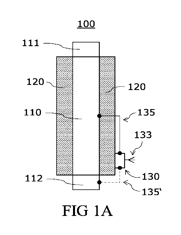
Fig. 1A shows a schematic cross-section through a power component 100. In the
exemplary
embodiment, power component 100 is a power fuse having an electrically
conductive element
110 as main functional component which is laterally surrounded by a ceramic
fuse body
forming the component housing 120. Fuse body 120 may e.g. be shaped as a
hollow cylinder.
The electrically conductive element is in electric contact with two electric
terminals 111, 112,
and may carry a current between the terminals 111, 112 and break the current
above a
predetermined threshold current. A sensor and emitter unit 130 having an
antenna 133 for
emitting electromagnetic signals is arranged on and attached to an outer
surface of fuse body
120. As indicated by a wiring 135, the sensor and emitter unit 130 may be
connected with
measuring tips arranged next to or even at the surface of the electrically
conductive element
110. Note that any wiring in the drawings may correspond to a wire, a pair of
wires or even
more than two wires.
Accordingly, sensor and emitter unit 130 may measure core temperature values
of the
electrically conductive element 110 during device operation, and emit the core
temperature
values encoded into an electromagnetic signal via antenna 133 to a reader (not
shown). For sake
16
CA 03171221 2022- 9-9
WO 2021/180419
PCT/EP2021/053416
of clarity, further optional details of power fuse 100 such as a filler are
also not shown in Fig.
1A.
This allows conta.ctlessly transferring the measured temperature values and
remote further
processing to at least characterize the operating state of power component
100.
As indicated by the dashed wiring 135', sensor and emitter unit 130 may
alternatively or in
addition measure temperature values of terminal 112 (or even both terminals)
and emit the
terminal temperature value(s) in encoded form with the electromagnetic signal.
The respective temperature values may be measured for a temperature range from
about -40 C
to about 125 C (for measuring core temperature) or from about -40 C to about
+85 C (for
measuring terminal temperature), and/or with an accuracy of at least .5 C.
Fig. 1B shows a schematic view of a section of a power component 100'. Power
component
100' is similar to power component 100 explained above with regard to Fig. 1A
and may also
be a power fuse. However, the sensor and emitter unit 130' of power component
100' is
implemented as an RFID-temperature sensor. RFID-temperature sensor 130' has a
sensor unit
131 with an appropriate measuring circuitry, and an emitter unit 132 with a
flat coiled antenna
133.
As shown in Fig. 1C illustrating a schematic view of a section of a power
component 100", the
sensor unit 131 and the emitter unit 132 of RFID-sensor 130" may be spaced
apart from each
other, but are functionally coupled with each other, typically via a wired
connection.
Fig. 1D shows a schematic cross-section through a power component 200. Power
component
200 is typically similar to the power components 100 to 100" explained above
with regard to
figures 1 A to 1C and typically also a power fuse, in particular a respective
semiconductor fuse.
However, in the exemplary embodiment of figure 1D, the sensor and emitter unit
230 attached
17
CA 03171221 2022- 9-9
WO 2021/180419
PCT/EP2021/053416
to fuse body (component housing) 220 is connected via respective wires 235
with both electrical
terminals 211, 212.
The sensor and emitter unit 230 is typically configured to measure the
voltages at the terminals
211, 212. Further, the sensor and emitter unit 230 may be configured to
determine a voltage
drop between the two terminals 211, 212.
As explained above, the sensor and emitter unit 230 may be implemented as a
Bluetooth-sensor
or an RFID-sensor, for example as an RFID voltage measuring sensor, in
particular a respective
battery free RFID tag in the exemplary embodiment.
More particular, the sensor and emitter unit 230 may be configured to measure
the AC voltage
drop across semiconductor fuse 200 and its main component (conductive element)
211,
respectively, even under high power conditions / in high power applications,
in particular in
high power rectifier applications (see also figures 2A, 2B).
The voltage measurement may e.g. be used to monitor current distribution
(online) in those
applications. Alternatively or in addition, information of the operational
state of fuse 200 may
be determined from the measured values.
The sensor and emitter unit 230 may be configured to measure AC voltage pulses
across the
fuse 200 and calculate respective RMS values that may be averaged. In this
regard it is noted
that the measuring voltage may not be a sinus waveshape, for example even
pulsed DC voltage
may be used, and can be distorted.
Further, the sensor and emitter unit 230 is typically protected in order not
to create any arc when
the (AC) fuse 200 is broken, and full voltage drop of e.g. 2 kV AC applies
across fuse 200 and
therefore the sensor and emitter unit 230. However, this typically depends on
the specifications
of the power semiconductor device to which semiconductor fuse 200 is to be
connected in series.
18
CA 03171221 2022- 9-9
WO 2021/180419
PCT/EP2021/053416
For example, the sensor and emitter unit 230 may fulfil one or more or even
all of the following
specifications:
Rated measuring voltage: 80 ... 250 mV;
Rated frequency: 50/60 Hz;
Measurement mode: RMS, average optional;
Measurement update cycle rate: <10 s;
Isolation voltage input/output: 5 kV;
Temperature measurement range: -40 ... >125 C;
Type: RFID;
Frequency range for communication with a reader: UHF; and
Size: several square centimeters, typically less than 25 cm2.
The sensor and emitter unit 230 may be placed similarly to an auxiliary
contact (not shown) on
the fuse body 220.
Further, the circuitry of sensor and emitter unit 230 is typically enclosed by
a non-conducting
housing material This is because it is typically used under high voltage (HV)
conditions, for
example in an HV electronic stack. Further the sensor and emitter unit 230 is
typically used in
an environment with a lot of metal (stainless steel, aluminum, copper) in the
near.
Optionally, sensor and emitter unit 230 is further configured for temperature
measurements as
explained above with respect to figures lA - 1C, in particular for measuring
the terminal
(connection) temperature.
Fig. 1E shows a schematic cross-section through a power component 300
implemented as a
vertical power semiconductor device, more particular as a power semiconductor
diode. This
indicated by the dashed line representing a PN junction between a p-type
semiconductor region
and an n-type semiconductor region of the semiconductor body 310, each of
which is in ohmic
contact with one of the two power terminals 311, 312.
19
CA 03171221 2022- 9-9
WO 2021/180419
PCT/EP2021/053416
In the exemplary embodiment, semiconductor body 310 is laterally enclosed by a
dielectric
component housing 320 which may e.g. be substantially ring-shaped (when seen
from above).
Further, a sensor and emitter unit 330 is arranged on and at a lateral outer
side of housing 320.
As indicated by the wiring 335, the sensor and emitter unit 330 is typically
functionally
connected with the semiconductor body 310 and configured to measure a core
temperature of
semiconductor body 310, more particular a temperature at least close to the PN
junction of
power diode 300.
For this purpose, an integrated resistive structure arranged at or close to
the rectifying junction
and at or close to a center of the semiconductor body with respect to a
central axis of
semiconductor body 310 which is typically at least substantially perpendicular
to the PN
junction (cylinder axis).
Alternatively or in addition, the sensor and emitter unit 330 may be
configured to measure the
voltages at the power terminals 311, 312 and/or to determine a voltage drop
between the power
terminals 311, 312. These measurements may e.g. be used to directly measure
current
imbalances between power diodes connected in parallel.
Furthermore, the sensor and emitter unit may be configured to measure the
temperature at
different points in the semiconductor body. Accordingly, a temperature profile
may be
determined during device operation. In particular in embodiments referring to
power MOSFETs
and power TGRTs typically having a plurality of respective cells, temperature
differences
between the cells may provide information on current distribution between the
cells and even
on ageing.
In further embodiments, the sensor and emitter unit may alternatively or in
addition be
configured to measure values of one or more other physical quantities
characterizing the
operating state of the respective device.
CA 03171221 2022- 9-9
WO 2021/180419
PCT/EP2021/053416
The sensor and emitter unit 330 may also be at least partly arranged in
component housing 320.
For example, the sensor and emitter unit 330 may be cast into a casting
compound used for
encasing semiconductor body 310.
Fig. 2A shows a schematic diagram of a power module 500 formed by two power
components
200, 300 connected in series, namely a power semiconductor diode 300 as
explained above with
regard to figure 1E and a corresponding semiconductor fuse 200 as explained
above with regard
to figure 1D.
For sake of clarity, the respective the sensor and emitting units which may be
used to measure
and contactlessly transmit values for the core temperature of power
semiconductor diode 300
and the terminal temperatures and the voltage drop across the fuse 200,
respectively, are not
shown in figure 2A. These values may be used to monitor power module 500 or
even several
power modules during operation.
The latter is illustrated in figure 2B showing a schematic diagram of an
exemplary 3-phase
power rectifier 600 made of six power modules 501-506 each of which typically
corresponds
to a power module 500 as explained with regard to figure 2A, and figure 3A
showing a
schematic diagram of an exemplary power rectifier 550 made N power modules 501-
50N (N
being a whole positive number that may be larger than 3, 7 or even 15) each of
which typically
corresponds to a power module 500 as explained with regard to figure 2A. The
illustrated power
modules 501-506, 501-50N may be considered as respective submodules each
comprising
and/or being made of a power semiconductor device and a power fuse connected
in series.
Based on the temperature measurements and voltage drop measurements of the
power fuses
200, respective currents II ¨ 16 flowing through each of the six modules 501-
506 (in Fig. 2A)
and respective currents II ¨ IN flowing through each of the N modules 501-50N
(in Fig. 3A),
respectively, may be determined with high accuracy as the voltage drops across
each of the
21
CA 03171221 2022- 9-9
WO 2021/180419
PCT/EP2021/053416
fuses 200 are measured and the resistance of each of the fuses 200 may
corrected in accordance
with the measured corresponding fuse temperature.
Additionally measuring the temperature of the power diodes 300 is not required
for determining
a current distribution within power rectifiers 550, 600, but may be used for
long-term
monitoring of the power devices, estimating ageing and/or scheduling
maintenance or repair.
In other words, it may be sufficient if only the power diodes 200 are provided
with respective
sensor and emitter units.
In other embodiments, it may be sufficient to only provide the power
semiconductor devices
with the respective sensor and emitter units.
This is illustrated in Fig. 3B showing a schematic diagram of an exemplary
power electronic
device 570 made of M typically at least substantially identical power modules
300' with M
being a whole positive number larger than 1, 3, 7 or even 15. Each power
module 300' may
corresponds to a power diode 300 as explained with regard to figure 1E. In
this embodiment,
power electronic device 570 may be a power rectifier. In embodiments referring
to power
electronic switching devices, each power module 300' may e.g. be a power
thyristor.
Based e.g. on temperature measurements using the sensor and emitter units of
the power
modules 300', an imbalance of the temperatures of the power module 300' may be
determined.
Based thereon and e.g. assuming at least substantially equal properties of the
power modules
300', an imbalance of the currents Ti ¨ Tm flowing through the M modules 501-
50M may be
determined.
In some applications it may even be sufficient to provide one of the power
modules with a
respective sensor and emitter unit.
As illustrated in Fig. 2C a monitoring and/or control system 701 for the power
component(s)
100 - 300 and the power module(s) 500 - 600 as explained above with regard to
figures lA to
22
CA 03171221 2022- 9-9
WO 2021/180419
PCT/EP2021/053416
2B typically has a receiving unit 710 configured to receive the
electromagnetic signals from the
power component(s) 100 - 300, to decode the measured value(s) of the physical
quantity(ies) T,
V, AV, and an evaluation unit 720 connected with the receiving unit 710, and
configured to the
determine or even analyze the respective operating state(s) based on the
decoded measured
value(s) of the physical quantity(ies) T, V. AV.
Receiving unit 710 and evaluation unit 720 may be formed by one device or may
be remote to
each other and/or connected with each other via a data network.
Depending on the determined/analysed operating state of one or more of the
power modules,
evaluation unit 720 may e.g. raise a warning message, and/or determine a
control parameter for
the power component(s) and use the determined control parameter for operating
the power
module(s). The latter is illustrated in figure 2C by the dashed arrow.
The system 700 formed by monitoring and/or control system 701 and the power
component(s)
100 - 300 and the power module(s) 500 - 600 may allow both controlling and
long-term
monitoring of the power component(s).
System 700 may perform the method 1000 illustrated in the flowchart of figure
2D.
In a first block 1100, a sensor and emitter unit of a power component, in
particular a sensor and
emitter unit of a power component as explained herein is used to measure a
value of a physical
quantity characterizing an operating state of the power component.
Thereafter, an electromagnetic signal in which the measured value of the
physical quantity is
encoded is emitted via an antenna of the sensor and emitter unit in a block
1200
Typically, the electromagnetic signal is received, and the encoded value is
decoded in a block
1300.
The blocks 1100 to 1300 may be performed several times, for example in regular
intervals,
and/or for several power components, typically in parallel.
23
CA 03171221 2022- 9-9
WO 2021/180419
PCT/EP2021/053416
The encoded value(s) is(are) typically used for determining and/or
characterizing the operating
state, determining a warning message, a maintenance recommendation and/or a
control
parameter for the power component(s).
Fig. 2E shows a flow chart of a method 2000 for manufacturing a power
component, in
particular a power component as explained herein.
In a block 2100, a main component configured to carry a power current, and a
sensor and emitter
unit are provided.
In a block 2200, the main component is provided with a dielectric component
housing and the
sensor and emitting unit. This is done such that an antenna of the sensor and
emitting unit is
attached with the component housing and spaced apart from the main component,
and that the
sensor and emitter unit can measure a value of a physical quantity which
characterises an
operating state of the main component and emit via the antenna an
electromagnetic signal, in
which the measured value of the physical quantity is encoded.
Fig. 3C shows a flow chart of a method 3000.
In a first block 3100, a power module as explained herein may be provided.
In a block 3200, a respective measured value of one or more physical
quantities is/are received
from one, typically from two or even all of the sensor and emitter units of
the power components
of the power module.
The measured value may in particular refer to a temperature of the respective
main component,
a voltage of at least one of the two respective electric terminals, or a
voltage drop across the
main component and the two terminals, respectively.
Thereafter, the received measured value(s) is/are further processed in a block
3300.
As indicated by the dashed arrow in Fig. 3C, blocks 3200, 3300 may be repeated
(several times),
for example periodically.
24
CA 03171221 2022- 9-9
WO 2021/180419
PCT/EP2021/053416
Further processing may include one or more of the following steps:
determining a temperature distribution of the main components,
monitoring the temperature distribution,
determining a current flow through one or more of the main components,
determining a current flow distribution between the main components,
monitoring the current flow and/or the current flow distribution, and
detecting an imbalance of the temperature distribution and/or the current flow
distribution.
For example, the (provided) power module may be a power module 570 as
explained above
with respect to Fig. 3B, or a power module 550, 600 as explained above with
respect to figures
2B, 3A. In embodiment referring to power module 550, 600, the current flow
and/or the current
flow distribution may be determined taking into account a given electric
resistance between the
electric terminals of the power fuses, in particular a respective cold
resistance of the power
fuses.
Alternatively or in addition, further processing may include one or more of
the following steps:
estimating an ageing of the power module or of one or more power components
thereof,
scheduling a maintenance or a repair for the power module,
determining at least one updated control parameter for operating the power
module,
and
using the at least one updated control parameter for controlling the power
module.
For example, a switching characteristics and/or a current strength of one or
more controllable
power components of the power module and the power electronic device,
respectively, may be
CA 03171221 2022- 9-9
WO 2021/180419
PCT/EP2021/053416
amended to better balance the current and/or the temperature distribution.
This may increase
the lifetime.
Estimating the ageing may be based on monitored peak loads and/or integrated
loads of the
power module and the power components thereof, respectively.
The monitored loads may refer thermal loads, current loads and combinations
thereof
Although various exemplary embodiments of the invention have been disclosed,
it will be
apparent to those skilled in the art that various changes and modifications
can be made which
will achieve some of the advantages of the invention without departing from
the spirit and scope
of the invention. It will be obvious to those reasonably skilled in the art
that other components
performing the same functions may be suitably substituted. It should be
mentioned that features
explained with reference to a specific figure may be combined with features of
other figures,
even in those cases in which this has not explicitly been mentioned.
Spatially relative terms such as "under", "below", "lower", "over", "upper"
and the like are
used for ease of description to explain the positioning of one element
relative to a second
element. These terms are intended to encompass different orientations of the
device in addition
to different orientations than those depicted in the figures. Further, terms
such as "first",
"second", and the like, are also used to describe various elements, regions,
sections, etc. and
are also not intended to be limiting. Like terms refer to like elements
throughout the description.
As used herein, the terms "having", "containing", "including", "comprising"
and the like are
open ended terms that indicate the presence of stated elements or features,
but do not preclude
additional elements or features. The articles "a", "an" and "the" are intended
to include the
plural as well as the singular, unless the context clearly indicates
otherwise.
With the above range of variations and applications in mind, it should be
understood that the
present invention is not limited by the foregoing description, nor is it
limited by the
26
CA 03171221 2022- 9-9
WO 2021/180419
PCT/EP2021/053416
accompanying drawings Instead, the present invention is limited only by the
following claims
and their legal equivalents.
27
CA 03171221 2022- 9-9
WO 2021/180419
PCT/EP2021/053416
Reference numbers
100 ¨ 300 power component
110, 210, 310 main component of power component
111, 112, 211, 212, 311, 312 electrical terminal
120, 220, 320 housing of power component
130, 230, 330 sensor and emitter unit
133 antenna
500 ¨ 600 power module
700 system
1000 - 3300 method, method steps
28
CA 03171221 2022- 9-9