Note: Descriptions are shown in the official language in which they were submitted.
ELECTRODE ASSEMBLY, BATTERY CELL, BATTERY, AND
METHOD AND APPARATUS FOR MANUFACTURING ELECTRODE
ASSEMBLY
TECHNICAL FIELD
This application relates to the field of batteries, and in particular, to an
electrode assembly, a
battery cell, a battery, and a method and apparatus for manufacturing an
electrode assembly.
BACKGROUND
A rechargeable battery may be referred to as a secondary battery, and is a
battery that can be
charged after being discharged to activate active materials for continuous
use. Rechargeable
batteries are widely used in electronic devices, such as mobile phones, laptop
computers, battery
motorcycles, electric vehicles, electric airplanes, electric ships, electric
toy cars, electric toy ships,
electric toy airplanes, and electric tools.
The rechargeable batteries may include nickel-cadmium batteries, nickel-
hydrogen batteries,
lithium-ion batteries, secondary alkaline zinc-manganese batteries, and the
like.
At present, most commonly used batteries in automobiles are lithium-ion
batteries. As
rechargeable batteries, the lithium-ion batteries have the advantages of small
size, high energy
density, high power density, large cycle count, long storage time, and so on.
The rechargeable battery includes an electrode assembly and an electrolyte.
The electrode
assembly includes a positive electrode plate, a negative electrode plate, and
a separator located
between the positive electrode plate and the negative electrode plate. The
positive electrode plate
may also be referred to as a cathode electrode plate, and a positive electrode
active material layer is
provided on two surfaces of the positive electrode plate. For example, a
positive electrode active
material of the positive electrode active material layer may be lithium
manganate oxide, lithium
cobalt oxide, lithium iron phosphate, or lithium nickel cobalt manganate. The
negative electrode
plate may also be referred to as an anode electrode plate, and a negative
electrode active material
layer is provided on two surfaces of the negative electrode plate. For
example, a negative electrode
active material of the negative electrode active material layer may be
graphite or silicon.
1
CA 03171539 2022- 9- 13
As a common abnormal phenomenon of lithium batteries, lithium precipitation
may affect
charging efficiency and energy density of lithium ions. In case of severe
lithium precipitation,
lithium crystals may be further formed, and the lithium crystals may pierce
the separator to cause an
internal short circuit and thermal runaway, severely affecting battery safety.
Therefore, how to reduce or avoid lithium precipitation and improve battery
safety has become
a concern in the industry.
SUMMARY
A plurality of aspects of this application provide an electrode assembly, a
battery cell, a battery,
and a method and apparatus for manufacturing an electrode assembly, so as to
overcome the
foregoing problem or at least partially resolve the foregoing problem.
A first aspect of this application provides an electrode assembly, including a
positive electrode
plate and a negative electrode plate, where the positive electrode plate and
the negative electrode
plate are wound or stacked to form a bend region.
The bend region is provided with a barrier layer; and at least part of the
barrier layer is located
between the positive electrode plate and the negative electrode plate that are
adjacent to each other,
and is used to prevent at least part of ions deintercalated from the positive
electrode plate from
being intercalated into the negative electrode plate in the bend region. The
barrier layer is provided
between the positive electrode plate and the negative electrode plate that are
adjacent to each other,
so that the barrier layer blocks at least part of ions deintercalated from a
positive electrode active
material layer of the positive electrode plate in the bend region during
charging, and the ions
blocked by the barrier layer cannot be intercalated into a negative electrode
active material layer of
the negative electrode plate adjacent to the positive electrode plate in the
bend region. In this way,
in a case that the negative electrode active material layer of the negative
electrode plate falls off,
lithium precipitation is reduced, thereby improving safety performance of
battery cells and
improving service life of the battery cells.
In some embodiments, the electrode assembly further includes a separator for
isolating the
positive electrode plate and the negative electrode plate that are adjacent to
each other; and the
barrier layer is attached to one or two surfaces of the positive electrode
plate, and/or the barrier
layer is attached to one or two surfaces of the negative electrode plate,
and/or the barrier layer is
attached to one or two surfaces of the separator. This can reduce positional
movement of the barrier
layer during use of the electrode assembly.
2
CA 03171539 2022- 9- 13
In some embodiments, the electrode assembly further includes a separator for
isolating the
positive electrode plate and the negative electrode plate that are adjacent to
each other; and the
barrier layer is independently provided between the positive electrode plate
and the separator that
are adjacent to each other in the bend region, or the barrier layer is
independently provided between
the negative electrode plate and the separator that are adjacent to each other
in the bend region. This
facilitates installation of the barrier layer.
In some embodiments, a porosity of the barrier layer is less than a porosity
of the separator. In
this way, the barrier layer can more effectively block passage of lithium
ions.
In some embodiments, the electrode assembly includes one positive electrode
plate and one
negative electrode plate; the one positive electrode plate and the one
negative electrode plate are
compacted and wound to form one winding structure; and the barrier layer is
provided between the
positive electrode plate and the negative electrode plate that are adjacent to
each other on at least an
innermost side of the bend region. In this way, lithium precipitation between
the positive electrode
plate and the negative electrode plate that are adjacent to each other on the
innermost side can be
reduced, improving safety performance.
In some embodiments, an innermost electrode plate in the bend region is a
negative electrode
plate. This can improve utilization efficiency of an active material of the
positive electrode plate.
In some embodiments, there are a plurality of discontinuous barrier layers;
and the plurality of
discontinuous barrier layers are spaced apart in a bending direction or the
plurality of discontinuous
barrier layers are spaced apart in a direction perpendicular to the bending
direction. In this way,
passage of some lithium ions can be blocked, reducing lithium precipitation
and also ensuring
energy density of the electrode assembly.
In some embodiments, a thickness of the barrier layer is 2 to 200 microns, or
5 to 100 microns.
This can ensure safety of the electrode assembly and also ensure energy
density of the electrode
assembly.
In some embodiments, the barrier layer is provided with at least one through
hole.
In some embodiments, the porosity of the barrier layer is 10% to 70%, or 20%
to 60%. This
can ensure safety of the electrode assembly and also ensure energy density of
the electrode
assembly.
In some embodiments, the thickness of the barrier layer is A microns, the
porosity of the
barrier layer is B, and A and B satisfy the following relationship: 3.5
microns<A/B<2000 microns;
or 7 microns<A/B<1000 microns. This can ensure safety of the electrode
assembly and also ensure
energy density of the electrode assembly.
3
CA 03171539 2022- 9- 13
In some embodiments, two ends, perpendicular to the bending direction, of the
negative
electrode active material layer of the negative electrode plate extends beyond
corresponding ends of
the positive electrode active material layer of the positive electrode plate.
This can ensure energy
density of the electrode assembly.
In some embodiments, the barrier layer includes two ends in a direction
perpendicular to the
bending direction, and one or two ends of the barrier layer extend beyond the
positive electrode
active material layer of the positive electrode plate. In this way, passage of
more lithium ions can be
blocked, reducing lithium precipitation.
In some embodiments, the barrier layer includes two ends in a direction
perpendicular to the
bending direction, and the negative electrode active material layer of the
negative electrode plate
extends beyond one or two ends of the barrier layer. In this way, passage of
some lithium ions can
be blocked, reducing lithium precipitation and also ensuring energy density of
the electrode
assembly.
In some embodiments, the barrier layer is disposed opposite a largest-
curvature portion of the
negative electrode plate. In this way, no lithium ions may be intercalated
into the largest-curvature
portion or only a small part of lithium ions are intercalated into the largest-
curvature portion,
thereby reducing lithium precipitation.
In some embodiments, the barrier layer includes at least one of the following:
inorganic oxide,
binder, and adhesive tape.
In some embodiments, two ends, extending in the bending direction, of the
barrier layer are
located in the bend region. In this way, passage of more lithium ions can be
blocked, reducing
lithium precipitation.
In some embodiments, the electrode assembly is provided with a flat region
connected to the
bend region.
One end, extending in the bending direction, of the barrier layer is located
in the flat region,
and the other end is located in the bend region; or two ends, extending in the
bending direction, of
the barrier layer are both located in the flat region.
A second aspect of this application provides a battery cell, including: a
housing, a cover plate,
and at least one electrode assembly according to at least one of the foregoing
embodiments.
The housing is provided with an accommodating cavity and an opening, and the
electrode
assembly is accommodated in the accommodating cavity; and
the cover plate is configured to close the opening of the housing.
A third aspect of this application provides a battery, including a box body
and at least one
battery cell, and the battery cell is received in the box body.
4
CA 03171539 2022- 9- 13
A fourth aspect of this application provides a method for manufacturing an
electrode assembly,
including:
providing a positive electrode plate, a negative electrode plate, and a
barrier layer;
and
winding or stacking the positive electrode plate and the negative electrode
plate to
form a bend region, where the bend region is provided with the barrier layer,
and at least
part of the barrier layer is located between the positive electrode plate and
the negative
electrode plate that are adjacent to each other, and is used to prevent at
least part of ions
deintercalated from the positive electrode plate from being intercalated into
the negative
electrode plate in the bend region.
In some embodiments, a separator for isolating the positive electrode plate
and the negative
electrode plate that are adjacent to each other is provided; and the
separator, the positive electrode
plate, and the negative electrode plate are wound or stacked together.
In some embodiments, before the separator, the positive electrode plate, and
the negative
electrode plate are wound or stacked together, the method further includes:
placing the barrier layer
on one or two surfaces of the positive electrode plate or the negative
electrode plate.
In some embodiments, the placing the barrier layer on one or two surfaces of
the positive
electrode plate or the negative electrode plate specifically includes:
attaching or applying the barrier
layer to one or two surfaces of the positive electrode plate or the negative
electrode plate.
A fifth aspect of this application provides a device for manufacturing an
electrode assembly,
including:
a first providing apparatus, configured to provide a positive electrode plate;
a second providing apparatus, configured to provide a negative electrode
plate;
a third providing apparatus, configured to provide a barrier layer; and
an assembly apparatus, configured to wind or stack the positive electrode
plate and
the negative electrode plate to form a bend region.
The bend region is provided with a barrier layer; and at least part of the
barrier layer is located
between the positive electrode plate and the negative electrode plate that are
adjacent to each other,
and is used to prevent at least part of ions deintercalated from the positive
electrode plate from
being intercalated into the negative electrode plate in the bend region.
In some embodiments, the device for manufacturing an electrode assembly
further includes a
fourth providing apparatus, configured to provide a separator for isolating
the positive electrode
plate and the negative electrode plate that are adjacent to each other, where
the assembly apparatus
CA 03171539 2022- 9- 13
is further configured to wind or stack the positive electrode plate, the
negative electrode plate, and
the separator to form the bend region.
In some embodiments, there are two third providing apparatuses, and the two
third providing
apparatuses each are configured to provide the barrier layer and attach or
apply the barrier layer to
two surfaces of the positive electrode plate or the negative electrode plate.
A sixth aspect of this application provides an electric apparatus, where the
electric apparatus is
configured to receive power supplied by a battery.
The foregoing description is merely an overview of the technical solutions in
the embodiments
of this application. In order to better understand the technical means in the
embodiments of this
application, to achieve implementation according to content of the
specification, and to make the
above and other objects, features and advantages in the embodiments of this
application more
comprehensible to understand, the following describes specific embodiments of
this application.
BRIEF DESCRIPTION OF DRAWINGS
To describe the technical solutions in the embodiments of this application
more clearly, the
following briefly describes the accompanying drawings required for describing
the embodiments.
Apparently, the accompanying drawings in the following description show merely
some
embodiments of this application, and a person of ordinary skill in the art may
still derive other
drawings from these accompanying drawings without creative efforts.
FIG. 1 is a schematic diagram of a three-dimensional structure of an electrode
assembly
according to an embodiment of this application;
FIG. 2 is a schematic structural diagram of a cross section of the electrode
assembly of FIG. 1
in a direction perpendicular to a winding axis K;
FIG. 3 is a schematic partial structural diagram of a bend region of an
electrode assembly
according to an embodiment of this application;
FIG. 4 is a schematic structural diagram of distribution of barrier layers
after a bend region of
an electrode assembly is flattened according to another embodiment of this
application;
FIG. 5 is a schematic structural diagram of another type of distribution of
barrier layers after a
bend region of an electrode assembly is flattened according to another
embodiment of this
application;
FIG. 6 is a schematic structural diagram of another type of distribution of
barrier layers after a
bend region of an electrode assembly is flattened according to another
embodiment of this
application;
6
CA 03171539 2022- 9- 13
FIG. 7 is a schematic structural diagram of a negative electrode plate
according to another
embodiment of this application;
FIG. 8 is a schematic structural diagram of a positive electrode plate
according to another
embodiment of this application;
FIG. 9 is a schematic structural diagram of a cross section in a direction A-A
in FIG. 8;
FIG. 10 is a schematic structural diagram of a cross section in a direction B-
B in FIG. 8;
FIG. 11 is a schematic structural diagram of a cross section perpendicular to
a winding axis of
a flat-shaped electrode assembly according to another embodiment of this
application;
FIG. 12 is a schematic structural diagram of a cross section perpendicular to
a winding axis of
another flat-shaped electrode assembly according to another embodiment of this
application;
FIG. 13 is a schematic structural diagram of a cross section perpendicular to
a winding axis of
another flat-shaped electrode assembly according to another embodiment of this
application;
FIG. 14 is a schematic structural diagram of a cross section perpendicular to
a winding axis of
another flat-shaped electrode assembly according to another embodiment of this
application;
FIG. 15 is a schematic structural diagram of a cross section perpendicular to
a winding axis of
another flat-shaped electrode assembly according to another embodiment of this
application;
FIG. 16 is a schematic structural diagram of a cross section perpendicular to
a winding axis of
another flat-shaped electrode assembly according to another embodiment of this
application;
FIG. 17 is a schematic structural diagram of a cross section perpendicular to
a winding axis of
another flat-shaped electrode assembly according to another embodiment of this
application;
FIG. 18 is a schematic structural diagram of a cross section perpendicular to
a winding axis of
a flat-shaped electrode assembly according to another embodiment of this
application;
FIG. 19 is a schematic structural diagram of a cross section perpendicular to
a winding axis of
a flat-shaped electrode assembly according to another embodiment of this
application;
FIG. 20 is a schematic structural diagram of a battery cell according to
another embodiment of
this application;
FIG. 21 is a schematic structural diagram of a battery module according to
another
embodiment of this application;
FIG. 22 is a schematic structural diagram of a battery according to another
embodiment of this
application;
FIG. 23 is a schematic structural diagram of an electric apparatus according
to another
embodiment of this application;
FIG. 24 is a schematic flowchart of a method for manufacturing an electrode
assembly
according to another embodiment of this application; and
7
CA 03171539 2022- 9- 13
FIG. 25 is a schematic structural diagram of a device for manufacturing an
electrode assembly
according to another embodiment of this application.
DETAILED DESCRIPTION OF EMBODIMENTS
To make the objectives, technical solutions, and advantages of the embodiments
of this
application clearer, the following clearly and completely describes the
technical solutions in the
embodiments of this application with reference to the accompanying drawings in
the embodiments
of this application. Apparently, the described embodiments are some but not
all of the embodiments
of this application. All other embodiments obtained by a person of ordinary
skill in the art based on
the embodiments of this application without creative efforts shall fall within
the protection scope of
this application.
Unless otherwise defined, all technical and scientific terms used herein shall
have the same
meanings as commonly understood by those skilled in the art to which this
application belongs. The
terms used in the specification of this application are merely intended to
describe the specific
embodiments but not intended to constitute any limitation on this application.
The terms "include",
"have" and any other variants in the specification, claims, and description of
accompanying
drawings of this application mean to cover the non-exclusive inclusion.
The term "embodiment" described herein means that specific features,
structures, or
characteristics in combination with descriptions of the embodiments may be
incorporated in at least
one embodiment of this application. The word "embodiment" in various positions
in the
specification does not necessarily refer to a same embodiment, or an
independent or alternative
embodiment that is exclusive of other embodiments. Persons skilled in the art
explicitly and
implicitly understand that the embodiments described herein may combine with
another
embodiments.
The term "and/or" in this specification describes only an association
relationship for describing
associated objects and represents that three relationships may exist. For
example, A and/or B may
represent the following three cases: A alone, both A and B, and B alone. In
addition, the character
"/" in this specification generally indicates an "or" relationship between the
associated objects.
In the descriptions of this application, it should be understood that the
orientations or
positional relationships indicated by the terms "center", "vertical",
"transverse", "length", "width",
"thickness", "upper", "lower", "front", "rear", "left", "right",
"perpendicular", "horizontal", "top",
"bottom", "inside", "outside", "clockwise", "counterclockwise", "axial", "
radial", "circumferential",
and the like are based on the orientations or positional relationships shown
in the accompanying
8
CA 03171539 2022- 9- 13
drawings, are merely intended to facilitate the descriptions of this
application and simplify the
descriptions, are not intended to indicate or imply that the apparatuses or
components mentioned in
this application must have specific orientations, or be constructed and
operated for a specific
orientation, and therefore shall not be construed as a limitation to this
application. In addition, the
terms "first", "second" and the like in the specification, claims or
description of accompanying
drawings of this application are used to distinguish between different objects
but not describe a
specific sequence, and can explicitly or implicitly include one or more
features. In the descriptions
of this application, unless otherwise specified, "plurality" means two or more
than two.
In the descriptions of this application, it should be noted that unless
otherwise specified and
defined explicitly, the terms "installment", "link", and "connection" should
be understood in their
general senses. For example, the terms may be a fixed connection, a detachable
connection, or an
integrated connection; or may be a mechanical connection or an electrical
connection; or may be a
direct connection, or an indirect connection through an intermediate medium;
or may be an internal
connection between two components. A person of ordinary skill in the art can
understand specific
meanings of these terms in this application based on specific situations.
In order to make a lithium-ion battery smaller in volume and higher in energy
density, a
positive electrode plate, a negative electrode plate, and a separator in an
electrode assembly of the
lithium-ion battery may be wound and then compacted. For example, FIG. 1 is a
schematic diagram
of a three-dimensional structure of an electrode assembly. The electrode
assembly includes a
negative electrode plate, a positive electrode plate, and a separator. The
negative electrode plate, the
positive electrode plate, and the separator are stacked and wound around a
winding axis K to form a
winding structure. The separator is an insulation film and used to isolate the
negative electrode plate
from the positive electrode plate to prevent short circuit of the negative
electrode plate and the
positive electrode plate. The winding structure of the electrode assembly is
of a flat shape. A
schematic structural diagram of a cross section of the electrode assembly in a
direction
perpendicular to the winding axis K may be shown in FIG. 2.
With reference to FIG. 1 and FIG. 2, the electrode assembly includes a flat
region 100 and
bend regions 200 located at two ends of the flat region 100. The flat region
100 is a region with a
parallel structure in the winding structure, that is, the negative electrode
plate 101, the positive
electrode plate 102, and the separator 103 in the flat region 100 are
substantially parallel to each
other. In other words, surfaces of the negative electrode plate 101, the
positive electrode plate 102,
and the separator 103 in the flat region 100 of the electrode assembly are all
flat. The bend region
200 is a region with a bending structure in the winding structure, that is,
the negative electrode plate
101, the positive electrode plate 102, and the separator 103 in the bend
region 200 are all bent. In
9
CA 03171539 2022- 9- 13
other words, surfaces of the negative electrode plate 101, the positive
electrode plate 102, and the
separator 103 in the bend region 200 of the electrode assembly are all curved.
The bend region 200
has a bending direction L, and the bending direction L can be understood as a
direction in which
surfaces of the electrode assembly in the bend region points to the flat
region. For example, the
bending direction Lisa winding direction of the winding structure in the bend
region 200.
A surface of the negative electrode plate 101 has a negative electrode active
material layer
composed of a negative electrode active material, and a surface of the
positive electrode plate 102
has a positive electrode active material layer composed of a positive
electrode active material. For
example, the positive electrode active material may be lithium manganate
oxide, lithium cobalt
oxide, lithium iron phosphate, or lithium nickel cobalt manganate, and the
negative electrode active
material may be graphite or silicon.
During charging of the lithium-ion battery, lithium ions are deintercalated
from the positive
electrode and intercalated into the negative electrode. However, some
exceptions may occur, for
example, insufficient space for lithium intercalation in the negative
electrode, excessively large
resistance for intercalation of lithium ions into the negative electrode,
excessively rapid
deintercalation of lithium ions from the positive electrode, inability of
intercalating deintercalated
lithium ions into the negative electrode active material layer of the negative
electrode plate in the
same amount, or lithium ions that cannot be intercalated into the negative
electrode plate obtaining
electrons only on the surface of the negative electrode. Consequently, a
silver-white metallic lithium
element is formed, which is referred to as lithium precipitation. Lithium
precipitation not only
reduces performance of lithium-ion batteries and greatly shortens the cycle
life, but also limits a fast
charging capacity of the lithium-ion batteries. In addition, when lithium
precipitation occurs in the
lithium-ion battery, resulting lithium metal is so active to react with the
electrolyte at a lower
temperature, causing a lower self-heating start temperature (Tonset) and a
higher self-heating rate,
and therefore severely affecting battery safety. Furthermore, in case of
severe lithium precipitation,
deintercalated lithium ions may form lithium crystals on the surface of the
negative electrode plate,
and the lithium crystals are prone to pierce the separator, to cause a risk of
short circuit to the
positive electrode plate and the negative electrode plate that are adjacent to
each other.
During the research and development process, the inventor found that lithium
precipitation
often occurs in the bend region of the electrode assembly. Through further
research, the inventor
found that lithium precipitation is attributed to falling-off of the active
material. The positive active
material is applied on the surface of the positive electrode plate, and the
negative active material is
applied on the surface of the negative electrode plate; however, the positive
electrode plate and the
negative electrode plate that are located in the bend region need to be bent,
and therefore the active
CA 03171539 2022- 9- 13
materials may fall off, which is referred to as powder falling-off. This
especially occurs on an
innermost-layer electrode plate in the bend region due to a largest bending
degree of the
innermost-layer electrode plate that easily causes falling-off of the active
material. Due to
falling-off of the active materials, especially falling-off of the active
material on the negative
electrode plate, lithium intercalation positions on the negative electrode
active material layer of the
negative electrode plate may be less than lithium ions that can be provided by
the positive electrode
active material layer of the positive electrode plate adjacent to the negative
electrode plate. As a
result, the lithium battery is prone to lithium precipitation during charging.
In view of this, this application is intended to provide an electrode
assembly. The electrode
assembly includes a negative electrode plate, a positive electrode plate, and
a separator. The
negative electrode plate, the positive electrode plate, and the separator may
be stacked and wound
in a winding axis to form a winding structure, for example, a flat-shaped
winding structure. The
negative electrode plate, the positive electrode plate, and the separator may
be continuously folded
in a zigzag manner after being stacked. Regardless of whether the electrode
assembly is formed in a
winding or zigzag manner, the electrode assembly includes a flat region and
bend regions
connecting two ends of the flat region. In order to reduce or avoid lithium
precipitation, a barrier
layer is provided between any positive electrode plate and negative electrode
plate that are adjacent
to each other in the bend region. The barrier layer is especially provided
between the positive
electrode plate and negative electrode plate that are adjacent to each other
on an innermost side of
the bend region. The barrier layer is used to block at least part of lithium
ions deintercalated from
the positive electrode active material layer of the positive electrode plate
in the bend region, so that
the ions blocked by the barrier layer cannot be intercalated into the negative
electrode active
material layer of the negative electrode adjacent to the positive electrode
plate in the bend region. In
this way, a quantity of lithium intercalation positions on the negative
electrode active material layer
of the negative electrode plate in the bend region is substantially the same
as a quantity of lithium
ions that can be provided by the positive electrode active material layer of
the positive electrode
plate adjacent to the negative electrode plate, thereby reducing or avoiding
lithium precipitation.
Regardless of whether the electrode assembly is formed in the winding or
zigzag manner, the
electrode assembly includes the flat region and the bend regions connecting
two ends of the flat
region. For ease of description, the electrode assembly in this embodiment is
described by using the
flat-shaped winding structure as an example. For example, one bend region C
and a flat region P of
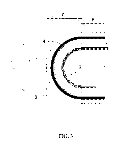
the flat-shaped winding structure may be shown in FIG. 3. FIG. 3 is a
schematic partial structural
diagram of a bend region of an electrode assembly according to an embodiment
of this application.
In the bend region C, the electrode assembly includes a positive electrode
plate 1, a negative
11
CA 03171539 2022- 9- 13
electrode plate 2, and a separator 3 for isolating the positive electrode
plate 1 and the negative
electrode plate 2. The separator 3 may be independently provided between the
positive electrode
plate 1 and the negative electrode plate 2 that are adjacent to each other, or
may be applied to a
surface of the positive electrode plate 1 or the negative electrode plate 2.
The separator 3 features electronic insulation and is used to isolate the
positive electrode plate
1 and the negative electrode plate 2 that are adjacent to each other, so as to
prevent a short circuit of
the positive electrode plate 1 and the negative electrode plate 2 that are
adjacent to each other. The
separator 3 is provided with a large number of through micropores to ensure
free passage of
electrolyte ions and good permeability of lithium ions. Therefore, the
separator 3 basically cannot
block passage of the lithium ions. For example, the separator 3 includes a
separator substrate and a
functional layer located on a surface of the separator substrate. The
separator substrate may be at
least one of polypropylene, polyethylene, ethylene-propylene copolymer,
polybutylene terephthalate,
and the like. The functional layer may be a mixture layer of ceramic oxide and
a binder.
For the electrode assembly in this embodiment of this application, the bend
region C is further
provided with a barrier layer 4; and at least part of the barrier layer 4 is
located between the positive
electrode plate 1 and the negative electrode plate 2 that are adjacent to each
other, and is used to
prevent at least part of ions deintercalated from the positive electrode plate
1 from being
intercalated into the negative electrode plate 2 in the bend region C.
Disposing the barrier layer 4 between the positive electrode plate 1 and the
negative electrode
plate 2 that are adjacent to each other in the bend region C can effectively
reduce or avoid lithium
precipitation. The barrier layer 4 is provided between the positive electrode
plate 1 and the negative
electrode plate 2 that are adjacent to each other, so that the barrier layer 4
blocks at least part of ions
deintercalated from a positive electrode active material layer (for example, a
positive electrode
active material layer in the bend region C) of the positive electrode plate 1
during charging, and the
ions blocked by the barrier layer 4 cannot be intercalated into a negative
electrode active material
layer of the negative electrode plate 2 in the bend region C. In this way,
when the negative electrode
active material layer of the negative electrode plate 2 falls off, lithium
precipitation is reduced. That
is, although the number of lithium intercalation positions on the negative
electrode plate 2 is
reduced due to falling-off of the negative electrode active material, lithium
precipitation can be
reduced or even avoided because the barrier layer 4 blocks at least part of
the lithium ions
deintercalated from the positive electrode plate 1 adjacent to the negative
electrode plate 2.
In another embodiment of this application, in order to block passage of
lithium ions, the barrier
layer 4 may be made of inorganic oxide and/or macromolecular polymer.
12
CA 03171539 2022- 9- 13
In another embodiment of this application, the inorganic oxide may be at least
one of
magnesium oxide (MgO), calcium oxide (CaO), boehmite, wollastonite, barium
sulfate (BaSO4),
calcium sulfate (CaSO4), calcium carbonate (CaCO3), aluminum oxide (A1203),
and silicon
dioxide (SiO2).
In another embodiment of this application, the macromolecular polymer may be
polypropylene
(polypropylene), polyvinyl chloride (Polyvinyl chloride, PVC), polyethylene
(polyethylene, PE),
epoxy resin, polyacrylate, and polyurethane rubber.
In another embodiment of this application, the barrier layer 4 may be adhesive
tape or adhesive
paper. The adhesive tape includes an adhesive and a substrate. The substrate
may be made of
polyethylene and/or ethylene-vinyl acetate copolymer (Ethylene Vinyl Acetate
Copolymer, EVA),
or the like. The adhesive paper is made of at least one of polyethylene
phthalate, polyvinylidene
fluoride, polyurethane, sodium polyacrylate, styrene butadiene rubber,
polyetherimide,
carboxymethyl cellulose, and acrylate.
In another embodiment of this application, one positive electrode plate 1 and
one negative
electrode plate 2 may be stacked and then wound or folded, or at least one
(for example, two or
more) positive electrode plate 1 and at least one (for example, two or more)
negative electrode plate
2 are stacked and then wound or folded, to form a bend region C. When the
electrode assembly is
provided with a plurality of positive electrode plates 1 and a plurality of
negative electrode plate 2
in the bend region C, the bend region C includes a structure in which positive
electrode plates 1 and
negative electrode plates 2 are alternately arranged, and the barrier layer 4
is included between at
least one positive electrode plate 1 and at least one negative electrode plate
2 that are adjacent to
each other. The positive electrode plate 1 and the negative electrode plate 2
that are adjacent to each
other in the bend region C indicate that one positive electrode plate 1 and
one negative electrode
plate 2 are adjacent in the bend region C, without another one positive
electrode plate 1 or another
one negative electrode plate 2 included in between.
In another embodiment of this application, in addition to the structure in
which the positive
electrode plate 1 and the negative electrode plate 2 are alternately arranged,
the bend region C (for
example, the innermost and/or outermost side of the bend region C) may
alternatively have a
structure in which no negative electrode plate 2 is sandwiched between two
adjacent positive
electrode plates 1, or a structure in which no positive electrode plate 1 is
sandwiched between two
adjacent negative electrode plates 2. In this case, no barrier layer 4 may be
provided between two
positive electrode plates 1 or two adjacent negative electrode plates 2, that
is, the barrier layer 4 is
provided between the positive electrode plate 1 and the negative electrode
plate 2 that are adjacent
to each other.
13
CA 03171539 2022- 9- 13
In another embodiment of this application, the innermost electrode plate in
the bend region C
of the electrode assembly is generally most bent, that is, the active material
of the innermost
electrode plate has a largest probability of falling-off or the active
material falls off most severely.
The innermost electrode plate may be a positive electrode plate 1 or a
negative electrode plate 2.
For example, when the innermost electrode plate is the negative electrode
plate 2, in order to reduce
lithium precipitation to a maximum extent, the barrier layer 4 is disposed
between the positive
electrode plate 1 and the negative electrode plate 2 that are adjacent to each
other on at least the
innermost side of the bend region C. In this way, lithium precipitation
between the positive
electrode plate and the negative electrode plate that are adjacent to each
other on the innermost side
can be reduced, improving safety performance. When the innermost electrode
plate in the bend
region C is the negative electrode plate 2, utilization efficiency of the
active material of the positive
electrode plate 1 can be improved.
The barrier layer 4 is located between the positive electrode plate 1 and the
negative electrode
plate 2 that are adjacent to each other. The barrier layer 4 may be
independently located between the
positive electrode plate 1 and the negative electrode plate 2 that are
adjacent to each other, or the
barrier layer 4 may be attached to any surface of the positive electrode plate
1, the negative
electrode plate 2, or the separator 3. That the barrier layer 4 may be
independently located between
the positive electrode plate 1 and the negative electrode plate 2 that are
adjacent to each other
means that the barrier layer 4 is stacked with each of the positive electrode
plate 1 and the negative
electrode plate 2 in a separated manner, not being in an adhering or coating
relationship. This
facilitates installation of the barrier layer 4. Attaching means adhering,
applying, or spraying. By
means of attaching, positional movement of the barrier layer 4 can be reduced
during use of the
battery cell.
For example, the barrier layer 4 is attached to one or two surfaces of the
positive electrode
plate 1, and/or the barrier layer 4 is attached to one or two surfaces of the
negative electrode plate 2.
In another embodiment of this application, the barrier layer 4 is
independently located between
the positive electrode plate 1 and the separator 3 that are adjacent to each
other in the bend region C,
or the barrier layer 4 is independently located between the negative electrode
plate 2 and the
separator 3 that are adjacent to each other in the bend region C, or the
barrier layer 4 is attached to
one or two surfaces of the separator 3. That the barrier layer 4 is
independently located between the
positive electrode plate 1 and the separator 3 that are adjacent to each other
in the bend region C, or
the barrier layer 4 is independently located between the negative electrode
plate 2 and the separator
3 that are adjacent to each other in the bend region C indicates that the
barrier layer 4 is separately
14
CA 03171539 2022- 9- 13
stacked with the positive electrode plate 1, the negative electrode plate 2,
and the separator 3, not
being in an adhering or coating relationship.
In another embodiment of this application, two ends, extending in the bending
direction L, of
the barrier layer 4 are both located in the bend region C, that is, the
barrier layer 4 is completely
located in the bend region C. In this embodiment, the electrode assembly
further includes a flat
region P connected to the bend region C. The bending direction L is a
direction along a curved
surface of the bend region C and pointing to the flat region P, and a
direction perpendicular to the
bending direction L is a direction vertical with the bending direction L.
In another embodiment of this application, one end, extending in the bending
direction L, of
the barrier layer 4 is located in the flat region P, and the other end is
located in the bend region C.
In another embodiment of this application, in order to block as many lithium
ions as possible,
the barrier layer 4 has a large area as possible in the bend region C. For
example, two ends,
extending in the bending direction L, of the barrier layer 4 are both located
in the flat region P, that
is, the barrier layer 4 is not only located in the bend region C but also
extends to the flat region P.
In another embodiment of this application, two ends, extending in the bending
direction L, of
the barrier layer 4 are both located at a junction between the bend region C
and the flat region P, or
two ends, extending in the bending direction L, of the barrier layer 4 are
both close to a junction
between the bend region C and the flat region P.
In another embodiment of this application, for the positive electrode plate 1
and the negative
electrode plate 2 that are adjacent to each other, when the negative electrode
plate 2 is located on
the innermost side of the bend region C, falling-off of the active material is
most severe in a
largest-curvature portion of the innermost negative electrode plate 2.
Therefore, regardless of how
the barrier layer 4 extends in the bending direction L, the barrier layer 4
prevents, as many as
possible, lithium ions deintercalated from the positive electrode plate 1 from
being intercalated into
the largest-curvature portion of the negative electrode plate 2, that is, the
barrier layer 4 is provided
opposite to the largest-curvature portion of the negative electrode plate 2,
so as to cover the
largest-curvature portion of the negative electrode plate 2. In this way, no
lithium ions may be
intercalated into the largest-curvature portion of the negative electrode
plate 2 or only a small
number of lithium ions are intercalated into the largest-curvature portion of
the negative electrode
plate 2, thereby reducing lithium precipitation.
In another embodiment of this application, the largest-curvature portion of
the negative
electrode plate 2 on the innermost side of the bend region C is a line (for
example, the line may be a
straight line) perpendicular to the bending direction L on a curved surface of
the negative electrode
plate 2 on the innermost side of the bend region C. A curvature of any point
on the line is greater
CA 03171539 2022- 9- 13
than a curvature of a curved surface, on both sides extending from the point
in the bending direction
L, of the negative electrode plate 2 on the innermost side of the bend region
C. For example, when
the negative electrode plate 2 is symmetrically bent in the bending direction
L in the bend region C,
the largest-curvature portion of the negative electrode plate 2 on the
innermost side of the bend
region C is a middle portion of the negative electrode plate 2 in the bend
region C.
A larger area of the barrier layer 4 in the bend region C indicates more
lithium ions that can be
blocked. However, more lithium ions blocked indicates lower energy density of
the bend region C,
resulting in lower energy density of the electrode assembly. Therefore, in
another embodiment of
this application, for the positive electrode plate 1 and the negative
electrode plate 2 that are adjacent
to each other in the bend region C, an appropriate amount of lithium ions can
be deintercalated from
the positive electrode plate 1 and intercalated into the negative electrode
plate 2, ensuring energy
density to some extent.
For example, as shown in FIG. 4, FIG. 4 is a schematic structural diagram of
distribution of
barrier layers after a bend region of an electrode assembly is flattened
according to another
embodiment of this application. A plurality of discontinuous barrier layers 4
are included between
the positive electrode plate 1 and the negative electrode plate 2 that are
adjacent to each other in the
bend region C. The plurality of discontinuous barrier layers are spaced apart
in the bending
direction L, so that part of lithium ions are not blocked by the barrier layer
4, that is, the part of
lithium ions pass between two adjacent barrier layers 4 and are intercalated
into the negative
electrode active material layer of the negative electrode plate 2. For
example, the plurality of
discontinuous barrier layers 4 are attached to the surface of the positive
electrode plate 1. In this
way, passage of some lithium ions can be blocked, reducing lithium
precipitation and also ensuring
energy density of the electrode assembly.
For another example, as shown in FIG. 5, FIG. 5 is a schematic structural
diagram of another
type of distribution of barrier layers after a bend region of an electrode
assembly is flattened
according to another embodiment of this application. A plurality of
discontinuous barrier layers 4
are included between the positive electrode plate 1 and the negative electrode
plate 2 that are
adjacent to each other in the bend region. The plurality of discontinuous
barrier layers 4 are spaced
apart in a direction K perpendicular to the bending direction L, so that part
of lithium ions are not
blocked by the barrier layer 4, that is, the part of lithium ions pass between
two adjacent barrier
layers 4 and are intercalated into the negative electrode active material
layer of the negative
electrode plate 2. For example, the plurality of discontinuous barrier layers
4 are attached to the
surface of the positive electrode plate 1. The direction K perpendicular to
the bending direction L
may be a width direction of the positive electrode plate 1 and the negative
electrode plate 2. When
16
CA 03171539 2022- 9- 13
the electrode assembly is a winding structure, the direction K perpendicular
to the bending direction
L is a winding axis direction of the winding structure.
For still another example, as shown in FIG. 6, FIG. 6 is a schematic
structural diagram of
another type of distribution of barrier layers after a bend region of an
electrode assembly is flattened
according to another embodiment of this application. The barrier layer 4 is
attached to the surface of
the positive electrode plate 1. The barrier layer 4 is provided with at least
one through hole 41,
configured to allow part of lithium ions to pass through and be intercalated
into the negative
electrode active material layer of the negative electrode plate 2.
In another embodiment of this application, the porosity of the barrier layer 4
is less than the
porosity of the separator 3, so that the barrier layer 4 can more effectively
block passage of lithium
ions. The porosity is a percentage of a pore volume of bulk material in a
total volume of the
material in a natural state. Generally, a test method for porosity is a test
method for true density.
In order to achieve a good balance between blocking lithium ions and
maintaining energy
density, the thickness of the barrier layer 4 is A micron, and the porosity of
the barrier layer 4 is B,
where A and B satisfy the following relationship: 3.5 microns<A/B< 2000
microns, optionally, 7
microns<A/B<1000 microns. This can ensure both safety of the electrode
assembly and energy
density of the electrode assembly, achieving a better balance between safety
performance and
energy density. A being excessively small indicates that the thickness of the
barrier layer 4 is
excessively small, and lithium crystals are prone to pierce the barrier layer
4 or even pierce the
separator 3, so that the barrier layer 4 is unable to block lithium ions,
possibly leading to a safety
risk. B being excessively large indicates that the porosity of the barrier
layer 4 is excessively large.
A larger porosity of the barrier layer 4 indicates more lithium ions that pass
through the barrier layer
4, possibly resulting in severe lithium precipitation. For example, A/B being
less than 3.5 indicates
that A is relatively small, that is, the thickness of the barrier layer 4 is
excessively small and B is
relatively large. In other words, the porosity of the barrier layer 4 is
excessively large, and the
barrier layer 4 loses the function of blocking lithium ions, possibly leading
to a safety risk. A/B
being greater than 2000 indicates that A is relatively large, that is, the
thickness of the barrier layer 4
is excessively large and B is relatively small. In other words, the porosity
of the barrier layer 4 is
excessively small, which severely affects energy density of the battery cell.
For example, the thickness of the barrier layer 4 is 2 to 200 microns (um);
optionally, the
thickness of the barrier layer 4 is 5 to 100 microns; further optionally, the
thickness of the barrier
layer 4 is 5 to 50 microns. This can ensure both safety of the electrode
assembly and energy density
of the electrode assembly, achieving a better balance between safety
performance and energy
density. For example, the thickness of the barrier layer 4 being less than 2
um indicates that the
17
CA 03171539 2022- 9- 13
thickness of the barrier layer 4 is excessively small. In case of severe
lithium precipitation, lithium
crystals pierce the barrier layer 4 and even pierce the separator 3, and
consequently the barrier layer
4 is unable to block lithium ions, leading to a safety risk. The thickness of
the barrier layer 4 being
greater than 500 um indicates that the thickness of the barrier layer 4 is
excessively large, leading to
an excessively large gap between the positive electrode plate 1 and the
negative electrode plate 2
that are adjacent to each other. The barrier layer 4 occupies space, which may
affect the energy
density of the electrode assembly. In addition, an excessively large gap
between two adjacent layers
may severely affect cycle performance.
The porosity of the barrier layer 4 is 10% to 70%; optionally, the porosity of
the barrier layer 4
is 20% to 60%. This can ensure both safety of the electrode assembly and
energy density of the
electrode assembly, achieving a better balance between safety performance and
energy density. For
example, when the porosity is less than 10%, most or all of the lithium ions
may be blocked by the
barrier layer 4, and cannot be intercalated into the negative electrode plate
2, thereby affecting the
energy density of the electrode assembly. However, when the porosity is
greater than 70%, most or
almost all of the lithium ions may pass through the barrier layer 4, leading
to a risk of lithium
precipitation. As a result, lithium crystals may pierce the barrier layer 4,
and the barrier layer 4 is
unable to block lithium ions, leading to a safety risk.
When the electrode assembly is of a winding structure, the width direction of
the positive
electrode plate 1 and the negative electrode plate 2 is parallel to the
winding axis direction, and the
width direction of the positive electrode plate 1 and the negative electrode
plate 2 is perpendicular
to the bending direction L. When the electrode assembly is not of a winding
structure, the width
direction of the positive electrode plate 1 and the negative electrode plate 2
is parallel to the
direction perpendicular to the bending direction L. For ease of subsequent
description, in this
embodiment, the width direction of the positive electrode plate 1 and the
negative electrode plate 2,
the direction perpendicular to the bending direction L, and the winding axis
direction are
collectively referred to as the direction K.
The structure of the negative electrode plate 2 may be shown in FIG. 7. FIG. 7
is a schematic
structural diagram of a negative electrode plate according to another
embodiment of this application.
The negative electrode plate 2 includes a negative electrode body portion 21
and a negative
electrode tab 22 extending outwards the negative electrode body portion 21 in
the direction K. At
least a partial region on a surface of the negative electrode body portion 21
in the direction K is a
negative electrode active material region 211. The negative electrode active
material region 211 is
used to coat the negative active material, and the negative electrode active
material may be graphite
or silicon.
18
CA 03171539 2022- 9- 13
In another embodiment of this application, the negative electrode active
material region 211 is
not only provided in the partial region on the surface of the negative
electrode body portion 21; the
negative electrode active material region 211 is also provided on a surface of
the negative electrode
tab 22 and a root region near the negative electrode body portion 21, that is,
a partial region of the
negative electrode tab 22 is the negative electrode active material region
211.
In another embodiment of this application, as shown in FIG. 7, the negative
electrode active
material region 211 covers the entire surface of the negative electrode body
portion 21 in the
direction K.
In another embodiment of this application, the positive electrode active
material may not cover
the entire surface of the positive electrode plate 1. For example, FIG. 8 is a
schematic structural
diagram of a positive electrode plate according to another embodiment of this
application.
The positive electrode plate 1 includes a positive electrode body portion 11
and at least one
positive electrode tab portion 12 extending outwards the positive electrode
body portion 11 in the
direction K. At least a partial region of the surface of the positive
electrode body portion 11 is a
positive electrode active material region 111. The positive electrode active
material region 111 may
be coated with a positive electrode active material, for example, the positive
electrode active
material may be a ternary material, lithium manganate oxide, or lithium iron
phosphate.
In another embodiment of this application, the surface of the positive
electrode body portion 11
further includes a first insulation layer coated region 112 adjacent to the
positive electrode active
material region 111, and the first insulation layer coated region 112 is
located at a side of the
positive electrode active material region 111 adjacent to the positive
electrode tab portion 12. The
first insulation layer coated region 112 is used for coating with an
insulation material, to insulate
and isolate the positive active material region 111 from the positive
electrode tab portion 12. For
example, FIG. 9 is a schematic structural diagram of a cross section in a
direction A-A in FIG. 8.
The positive electrode active material region 111 is provided on two surfaces
of a current collector
of the positive electrode plate 1, and the positive electrode tab portion 12
is a part of the current
collector 10 of the positive electrode plate 1. The current collector 10 may
be made of aluminum.
For example, the positive electrode active material region 111 and the first
insulation layer
coated region 112 are distributed at two ends, in the width direction (the
direction K) of the positive
electrode body portion 11, of the surface of the positive electrode body
portion 11, and the positive
electrode tab portion 12 and the first insulation layer coated region 112
belongs to the same end of
the positive electrode body portion 11.
In another embodiment of this application, the positive electrode active
material region 111
and the first insulation layer coated region 112 are two substantially
parallel regions on the surface
19
CA 03171539 2022- 9- 13
of the positive electrode body portion 11, and are distributed as two layers
on the surface of the
positive electrode body portion 11 in the direction K.
In another embodiment of this application, the first insulation layer coated
region 112 may be
located at a joint portion between the positive electrode body portion 11 and
the positive electrode
tab portion 12. For example, the first insulation layer coated region 112 is
located on the surface of
the positive electrode body portion 11 and the joint portion between the
positive electrode body
portion 11 and the positive electrode tab portion 12, and is used to isolate
the surface of the positive
electrode tab portion 12 from the positive electrode active material region
111. In another
embodiment of this application, the first insulation layer coated region 112
is provided on the
surface of the positive electrode body portion 11, and a second insulation
layer coated region 121 is
also provided in the root region of the positive electrode tab portion 12
close to the positive
electrode body portion 11. The second insulation layer coated region 121 are
used for coating of an
insulation material.
In another embodiment of this application, an insulation material is applied
to the surface of
the first insulation layer coated region 112, and the insulation material
includes an inorganic filler
and a binder. The inorganic filler includes one or more of boehmite, aluminum
oxide, magnesium
oxide, titanium dioxide, zirconium oxide, silicon dioxide, silicon carbide,
boron carbide, calcium
carbonate, aluminum silicate, calcium silicate, potassium titanate, and barium
sulfate. The binder
includes one or more of polyvinylidene fluoride, polyacrylonitrile,
polyacrylic acid, polyacrylate,
polyacrylic acid-acrylate, polyacrylonitrile-acrylic acid, and
polyacrylonitrile-acrylate.
In another embodiment of this application, each positive electrode plate 1 may
include one,
two, or more than two positive electrode tab portions 12. When the positive
electrode plate 1
includes two or more positive tab portions 12, all the positive pole tab
portions 12 are located on the
same side of the positive electrode plate 1 in the direction K.
With reference to FIG. 7 and FIG. 8, when the positive electrode plate 1 and
the negative
electrode plate 2 are stacked, two ends of the negative electrode active
material region 211 of the
negative electrode plate 2 in the direction K extend beyond corresponding ends
of the positive
electrode active material region 111 of the adjacent positive electrode plate
1. This can ensure the
energy density of the electrode assembly. For example, the two ends of the
negative electrode active
material region 211 in the direction K are a first end 23 and a second end 24,
and the two ends of
the positive electrode active material region 111 in the direction K are a
third end 13 and a fourth
end 14. The first end 23 of the negative electrode active material region 211
and the third end 13 of
the positive electrode active material region 111 are located on the same side
of the electrode
assembly in the direction K, and the first end 23 of the negative electrode
active material region 211
CA 03171539 2022- 9- 13
extends beyond the third end 13 of the positive electrode active material
region 111 in the direction
K. The second end 24 of the negative electrode active material region 211 and
the fourth end 14 of
the positive electrode active material region 111 are located on the other
side of the electrode
assembly in the direction K, and the second end 24 of the negative electrode
active material region
211 extends beyond the fourth end 14 of the positive electrode active material
region 111 in the
direction K.
A size by which the two ends of the negative electrode active material region
211 extending
beyond the corresponding ends of the positive electrode active material region
111 along the
winding axis K may be the same or different. For example, an exceeding size
ranges from 0.2 mm
to 5 mm.
As shown in FIG. 10, FIG. 10 is a schematic structural diagram of a cross
section in a direction
B-B in FIG. 8. With reference to FIG. 8, the barrier layer 4 is attached to
the surface of the positive
electrode active material region 111, that is, the surface of the positive
electrode active material
layer.
In order to block lithium ions and reduce costs, the barrier layer 4 includes
a fifth end 42 and a
sixth end 43 in the direction perpendicular to the bending direction (which is
the direction K), and
the fifth end 42 of the barrier layer 4 extends beyond the positive electrode
active material layer of
the positive electrode plate 1, and/or the sixth end 43 of the barrier layer 4
exceeds beyond the
positive electrode active material layer. To be specific, the fifth end 42 of
the barrier layer 4 exceeds
the third end 13 of the positive electrode active material region 111 in the
direction K, and/or the
sixth end 43 of the barrier layer 4 extends beyond the fourth end 14 of the
positive electrode active
material region 111 in the direction K, for example, the exceeding size ranges
from 0.2 mm to 5 mm.
In this way, passage of more lithium ions can be blocked, reducing lithium
precipitation.
In another embodiment of this application, both the fifth end 42 and the sixth
end 43 of the
barrier layer 4 do not exceed the corresponding ends of the negative electrode
active material layer
of the negative electrode plate 2. That is, the first end 23 of the negative
electrode active material
region of the negative electrode plate 2 extends beyond the fifth end 42 of
the barrier layer 4, and/or
the second end 24 of the negative electrode active material region of the
negative electrode plate 2
extends beyond the sixth end 43 of the barrier layer 4. In this way, lithium
ions can be intercalated
into a portion of the negative electrode plate 2 extending beyond the barrier
layer 4, ensuring the
energy density of the electrode assembly.
The foregoing embodiments briefly describe only a positional relationship
between the barrier
layer and the positive electrode plate, a positional relationship between the
barrier layer and the
negative electrode plate, and a structural characteristic of the barrier
layer. For better understanding
21
CA 03171539 2022- 9- 13
on the positional relationship between the barrier layer and the positive
electrode plate, the
positional relationship between the barrier layer and the negative electrode
plate, and the structure
of the barrier layer, the following describes in detail several electrode
assemblies with a winding
structure.
As shown in FIG. 11, FIG. 11 is a schematic structural diagram of a cross
section
perpendicular to a winding axis of a flat-shaped electrode assembly according
to another
embodiment of this application. The electrode assembly includes a negative
electrode plate 91, a
positive electrode plate 92, a separator 93, a first barrier layer 94, a
second barrier layer 95, and a
third barrier layer 96. The separator 93 is located between the negative
electrode plate 91 and the
positive electrode plate 92, and there are two separators 93, indicated by two
winding dashed lines
in the cross-sectional view of the electrode assembly in FIG. 11. The negative
electrode plate 91,
the positive electrode plate 92, and the separator 93 are stacked and then
wound into a flat-shaped
winding structure around the winding axis.
For related technical features of the negative electrode plate 91, the
positive electrode plate 92,
and the separator 93 in this embodiment, refer to the descriptions of the
embodiments
corresponding to FIGs. 1 to 10. Details are not repeated herein.
In this embodiment, the winding structure of the electrode assembly includes a
flat region 9A,
and a first bend region 9B1 and a second bend region 9B2 that are located on
two sides of the flat
region 9A. Division of the flat region 9A from the first bend region 9B1 and
the second bend region
9B2 is separately denoted by a straight dotted line.
The negative electrode plate 91 and the positive electrode plate 92 included
in the first bend
region 9B1 and the second bend region 9B2 of the electrode assembly are
alternately stacked in
sequence. The separator 93 is provided between the negative electrode plate 91
and the positive
electrode plate 92 that are adjacent to each other. Innermost electrode plates
in the first bend region
9B1 and the second bend region 9B2 are both the negative electrode plate 91. A
barrier layer is
provided (attached to) on inner surfaces of at least innermost positive
electrode plates 92 in the first
bend region 9B1 and the second bend region 962. For example, a barrier layer
is provided (attached
to) on an inner surface of each layer of positive electrode plate 92 in the
first bend region 9B1 and
the second bend region 9132. In this embodiment, the inner surface of the
positive electrode plate 92
is a surface of the positive electrode plate 92 facing toward the winding
axis, or a surface facing
toward inside of the winding structure.
For example, the first bend region 9B1 has a plurality of layers of electrode
plates, such as
three layers of electrode plates. An innermost-layer electrode plate (also
referred to as the first layer)
and an outermost-layer electrode plate (also referred to as the third layer)
of the first bend region
22
CA 03171539 2022- 9- 13
9B1 are both the negative electrode plate 91, and an electrode plate (also
referred to as the
second-layer electrode plate) between the innermost-layer electrode plate and
the outermost-layer
electrode plate is the positive electrode plate 92. The positive electrode
plate 92 is a positive
electrode plate on the innermost side of the first bend region 961, and the
first barrier layer 94 is
attached to an inner surface of the positive electrode plate 92 in the first
bend region 961.
The second bend region 9B2 has a plurality of layers of electrode plates, such
as five layers of
electrode plates. In a direction from inside to outside of the winding
structure, the negative
electrode plate 91 and the positive electrode plate 92 in the second bend
region 9B2 are alternately
stacked in sequence. An innermost-layer electrode plate in the second bend
region 9B2 is the
negative electrode plate 91, and a barrier layer is attached to an inner
surface of each layer of
positive electrode plate 92 in the second bend region 962.
For example, in the direction from inside to outside of the winding structure,
the second bend
region 9B2 sequentially includes the first-layer, second-layer, third-layer,
fourth-layer, and
fifth-layer electrode plates. The first-layer, third-layer, and fifth-layer
electrode plates are the
negative electrode plate 91; and the second-layer and fourth-layer electrode
plates are the positive
electrode plate 92. A barrier layer is attached to the inner surface of each
layer of layer of positive
electrode plate 92 in the second bend region 962. For example, the second
barrier layer 95 is
attached to an inner surface of the second-layer electrode plate (which is the
positive electrode plate
92) in the second bend region 962. For example, the third barrier layer 96 is
attached to an inner
surface of the fourth-layer electrode plate (which is the positive electrode
plate 92) in the second
bend region 962.
In this embodiment, two ends of each of the first barrier layer 94, the second
barrier layer 95,
and the third barrier layer 96 in the bending direction (that is, in the
winding direction) are located
at the junctions between the bend region and the flat region. For example, two
ends of the first
barrier layer 94 in the winding direction are separately located at the
junction between the first bend
region 9B1 and the flat region 9A, and two ends of each of the second barrier
layer 95 and the third
barrier layer 96 in the winding direction are separately located at the
junction between the second
bend region 9B2 and the flat region 9A.
In this embodiment, for related content of functions, structures, and
distribution of the first
barrier layer 94, the second barrier layer 95, and the third barrier layer 96,
refer to related content of
the barrier layer described in the embodiments of FIGs. 1 to 10. Details are
not repeated herein.
As shown in FIG. 12, FIG. 12 is a schematic structural diagram of a cross
section
perpendicular to a winding axis of another flat-shaped electrode assembly
according to another
embodiment of this application. The electrode assembly includes a negative
electrode plate 1001, a
23
CA 03171539 2022- 9- 13
positive electrode plate 1002, a separator 1003, a first barrier layer 1004, a
second barrier layer
1005, and a third barrier layer 1006. The separator 1003 is located between
the negative electrode
plate 1001 and the positive electrode plate 1002. The negative electrode plate
1001, the positive
electrode plate 1002, and the separator 1003 are stacked and then wound into a
flat-shaped winding
structure around the winding axis.
For related technical features of the negative electrode plate 1001, the
positive electrode plate
1002, and the separator 1003 in this embodiment, refer to the descriptions of
the embodiments
corresponding to FIGs. 1 to 10. Details are not repeated herein.
In this embodiment, the winding structure of the electrode assembly includes a
flat region 10A,
and a first bend region 10B1 and a second bend region 10132 that are located
on two sides of the flat
region 10A.
The electrode assembly in this embodiment is basically similar to the
electrode assembly
described in the embodiment corresponding to FIG. 11, and the difference may
be as follows:
A barrier layer is provided (attached to) on outer surfaces of at least
innermost positive
electrode plates 1002 in the first bend region 10B1 and the second bend region
1062. For example,
a barrier layer is provided (attached to) on an outer surface of each layer of
positive electrode plate
1002 in the first bend region 10B1 and the second bend region 1062. In this
embodiment, the outer
surface of the positive electrode plate 1002 is a surface of the positive
electrode plate 1002 facing
away from the winding axis, or a surface facing away from inside of the
winding structure.
For example, the first barrier layer 1004 is attached to an outer surface of
the positive electrode
plate 1002 in the first bend region 1061.
For example, the second barrier layer 1005 is attached to an outer surface of
the second-layer
electrode plate (which is the positive electrode plate 1002) in the second
bend region 1062. For
example, a third barrier layer 1006 is attached to an outer surface of the
fourth-layer electrode plate
(which is the positive electrode plate 1002) in the second bend region 10132.
In this embodiment, two ends of the first barrier layer 1004 in the winding
direction are located
at the junctions between the first bend region 10B1 and the flat region 10A,
and two ends of each of
the second barrier layer 1005 and the third barrier layer 1006 in the winding
direction are located at
the junctions between the second bend region 10132 and the flat region 10A.
In this embodiment, for related content of functions, structures, and
distribution of the first
barrier layer 1004, the second barrier layer 1005, and the third barrier layer
1006, refer to related
content of the barrier layer described in the embodiments of FIGs. 1 to 10.
Details are not repeated
herein.
24
CA 03171539 2022- 9- 13
As shown in FIG. 13, FIG. 13 is a schematic structural diagram of a cross
section
perpendicular to a winding axis of another flat-shaped electrode assembly
according to another
embodiment of this application. The electrode assembly includes a negative
electrode plate 1101, a
positive electrode plate 1102, a separator 1103, a first barrier layer 1104, a
second barrier layer 1105,
a third barrier layer 1106, a fourth barrier layer 1107, and a fifth barrier
layer 1108. The separator
1103 is located between the negative electrode plate 1101 and the positive
electrode plate 1102. The
negative electrode plate 1101, the positive electrode plate 1102, and the
separator 1103 are stacked
and then wound into a flat-shaped winding structure around the winding axis.
For related technical features of the negative electrode plate 1101, the
positive electrode plate
1102, and the separator 1103 in this embodiment, refer to the descriptions of
the embodiments
corresponding to FIGs. 1 to 10. Details are not repeated herein.
In this embodiment, the winding structure of the electrode assembly includes a
flat region 11A,
and a first bend region 11131 and a second bend region 1162 that are located
on two sides of the flat
region 11A.
The electrode assembly in this embodiment is basically similar to the
electrode assembly
described in the embodiment corresponding to FIG. 11, and the difference may
be as follows:
A barrier layer is provided (attached to) on inner surfaces of at least
innermost negative
electrode plates 1101 in a first bend region 1161 and a second bend region
11132. For example, a
barrier layer is provided on an inner surface of each layer of negative
electrode plate 1101 in the
first bend region 11131 and the second bend region 11132. In this embodiment,
the inner surface of
the negative electrode plate 1101 is a surface of the negative electrode plate
1101 facing toward the
winding axis, or a surface facing toward inside of the winding structure.
For example, the first barrier layer 1104 is attached to an inner surface of
an innermost-layer
electrode plate (which is the negative electrode plate 1101) in the first bend
region 1161, and the
second barrier layer 1105 is attached to an inner surface of an outermost-
layer electrode plate
(which is the negative electrode plate 1101).
For example, the third barrier layer 1106 is attached to an inner surface of
the first-layer
electrode plate (which is the negative electrode plate 1101) in the second
bend region 11132. The
fourth barrier layer 1107 is attached to an inner surface of the third-layer
electrode plate (which is
the negative electrode plate 1101) in the second bend region 11132. The fifth
barrier layer 1108 is
attached to an inner surface of the fifth-layer electrode plate (which is the
negative electrode plate
1101) in the second bend region 11132.
In this embodiment, two ends of each of the first barrier layer 1104 and the
second barrier
layer 1105 in the winding direction are located at the junctions between the
first bend region 11131
CA 03171539 2022- 9- 13
and the flat region 11A, and two ends of each of the third barrier layer 1106,
the fourth barrier layer
1107, and the fifth barrier layer 1108 in the winding direction are located at
the junctions between
the second bend region 1162 and the flat region 11A.
In this embodiment, for related content of functions, structures, and
distribution of the first
barrier layer 1104, the second barrier layer 1105, and the third barrier layer
1106, the fourth barrier
layer 1107, and the fifth barrier layer 1108, refer to related content of the
barrier layer described in
the embodiments of FIGs. 1 to 10. Details are not repeated herein.
As shown in FIG. 14, FIG. 14 is a schematic structural diagram of a cross
section
perpendicular to a winding axis of another flat-shaped electrode assembly
according to another
embodiment of this application. The electrode assembly includes a negative
electrode plate 1201, a
positive electrode plate 1202, a separator 1203, a first barrier layer 1204, a
second barrier layer
1205, a third barrier layer 1206, a fourth barrier layer 1207, and a fifth
barrier layer 1208. The
separator 1203 is located between the negative electrode plate 1201 and the
positive electrode plate
1202. The negative electrode plate 1201, the positive electrode plate 1202,
and the separator 1203
are stacked and then wound into a flat-shaped winding structure around the
winding axis.
For related technical features of the negative electrode plate 1201, the
positive electrode plate
1202, and the separator 1203 in this embodiment, refer to the descriptions of
the embodiments
corresponding to FIGs. 1 to 10. Details are not repeated herein.
In this embodiment, the winding structure of the electrode assembly includes a
flat region 12A,
and a first bend region 12B1 and a second bend region 12132 that are located
on two sides of the flat
region 12A.
The electrode assembly in this embodiment is basically similar to the
electrode assembly
described in the embodiment corresponding to FIG. 11, and the difference may
be as follows:
A barrier layer is provided (attached to) on outer surfaces of at least
innermost negative
electrode plates 1201 in the first bend region 12B1 and the second bend region
1262. For example,
a barrier layer is provided on an outer surface of each layer of negative
electrode plate 1201 in the
first bend region 12B1 and the second bend region 1262. In this embodiment,
the outer surface of
the negative electrode plate 1201 is a surface of the negative electrode plate
1201 facing away from
the winding axis, or a surface facing away from inside of the winding
structure.
For example, the first barrier layer 1204 is attached to an outer surface of
an innermost-layer
electrode plate (which is the negative electrode plate 1201) in the first bend
region 1261, and the
second barrier layer 1205 is attached to an outer surface of an outermost-
layer electrode plate
(which is the negative electrode plate 1201).
26
CA 03171539 2022- 9- 13
For example, the third barrier layer 1206 is attached to an outer surface of
the first-layer
electrode plate (which is the negative electrode plate 1201) in the second
bend region 1262. The
fourth barrier layer 1207 is attached to an outer surface of the third-layer
electrode plate (which is
the negative electrode plate 1201) in the second bend region 1262. The fifth
barrier layer 1208 is
attached to an outer surface of the fifth-layer electrode plate (which is the
negative electrode plate
1201) in the second bend region 1262.
In this embodiment, two ends of each of the first barrier layer 1204 and the
second barrier
layer 1205 in the winding direction are located at the junctions between the
first bend region 12B1
and the flat region 12A, and two ends of each of the third barrier layer 1206,
the fourth barrier layer
1207, and the fifth barrier layer 1208 in the winding direction are located at
the junctions between
the second bend region 12132 and the flat region 12A.
In this embodiment, for related content of functions, structures, and
distribution of the first
barrier layer 1204, the second barrier layer 1205, and the third barrier layer
1206, the fourth barrier
layer 1207, and the fifth barrier layer 1208, refer to related content of the
barrier layer described in
the embodiments of FIGs. 1 to 10. Details are not repeated herein.
As shown in FIG. 15, FIG. 15 is a schematic structural diagram of a cross
section
perpendicular to a winding axis of another flat-shaped electrode assembly
according to another
embodiment of this application. The electrode assembly includes a negative
electrode plate 1301, a
positive electrode plate 1302, a separator 1303, and a plurality of barrier
layers 1304. The separator
1303 is located between the negative electrode plate 1301 and the positive
electrode plate 1302. The
negative electrode plate 1301, the positive electrode plate 1302, and the
separator 1303 are stacked
and then wound into a flat-shaped winding structure around the winding axis.
For related technical features of the negative electrode plate 1301, the
positive electrode plate
1302, and the separator 1303 in this embodiment, refer to the descriptions of
the embodiments
corresponding to FIGs. 1 to 10. Details are not repeated herein.
In this embodiment, the winding structure of the electrode assembly includes a
flat region 13A,
and a first bend region 13B1 and a second bend region 13132 that are located
on two sides of the flat
region 13A.
The electrode assembly in this embodiment is basically similar to the
electrode assembly
described in the embodiment corresponding to FIG. 11, and the difference may
be as follows:
The barrier layer 1304 is provided on inner surfaces of at least innermost
separators 1303 in
the first bend region 13B1 and the second bend region 1362. For example, the
barrier layer 1304 is
provided on an inner surface of each layer of separator 1303 in the first bend
region 13B1 and the
second bend region 1362. In this embodiment, the inner surface of the
separator 1303 is a surface
27
CA 03171539 2022- 9- 13
of the separator 1303 facing toward the winding axis, or a surface facing
toward inside of the
winding structure.
In this embodiment, two ends of each barrier layer 1304 in the winding
direction in the first
bend region 13B1 are located at the junctions between the first bend region
13B1 and the flat region
13A, and two ends of each barrier layer 1304 in the winding direction in the
second bend region
13132 are located at the junctions between the second bend region 13B2 and the
flat region 13A.
In this embodiment, for related content of functions, structures, and
distribution of each barrier
layer 1304, refer to related content of the barrier layer described in the
embodiments of FIGs. 1 to
10. Details are not repeated herein.
As shown in FIG. 16, FIG. 16 is a schematic structural diagram of a cross
section
perpendicular to a winding axis of another flat-shaped electrode assembly
according to another
embodiment of this application. The electrode assembly includes a negative
electrode plate 1401, a
positive electrode plate 1402, a separator 1403, and a plurality of barrier
layers 1404. The separator
1403 is located between the negative electrode plate 1401 and the positive
electrode plate 1402. The
negative electrode plate 1401, the positive electrode plate 1402, and the
separator 1403 are stacked
and then wound into a flat-shaped winding structure around the winding axis.
For related technical features of the negative electrode plate 1401, the
positive electrode plate
1402, and the separator 1403 in this embodiment, refer to the descriptions of
the embodiments
corresponding to FIGs. 1 to 10. Details are not repeated herein.
In this embodiment, the winding structure of the electrode assembly includes a
flat region 14A,
and a first bend region 14B1 and a second bend region 14132 that are located
on two sides of the flat
region 14A.
The electrode assembly in this embodiment is basically similar to the
electrode assembly
described in the embodiment corresponding to FIG. 11, and the difference may
be as follows:
The barrier layer 1404 is provided on outer surfaces of at least innermost
separators 1403 in
the first bend region 14B1 and the second bend region 1462. For example, the
barrier layer 1404 is
provided on an outer surface of each layer of separator 1403 in the first bend
region 14B1 and the
second bend region 1462. In this embodiment, the outer surface of the
separator 1403 is a surface
of the separator 1403 facing away from the winding axis, or a surface facing
away from inside of
the winding structure.
In this embodiment, two ends of each barrier layer 1404 in the winding
direction in the first
bend region 14B1 are located at the junctions between the first bend region
14B1 and the flat region
14A, and two ends of each barrier layer 1404 in the winding direction in the
second bend region
14132 are located at the junctions between the second bend region 14132 and
the flat region 14A.
28
CA 03171539 2022- 9- 13
In this embodiment, for related content of functions, structures, and
distribution of each barrier
layer 1404, refer to related content of the barrier layer described in the
embodiments of FIGs. 1 to
10. Details are not repeated herein.
As shown in FIG. 17, FIG. 17 is a schematic structural diagram of a cross
section
perpendicular to a winding axis of another flat-shaped electrode assembly
according to another
embodiment of this application. The electrode assembly includes a negative
electrode plate 1501, a
positive electrode plate 1502, a separator 1503, and a plurality of barrier
layers 1504. The separator
1503 is located between the negative electrode plate 1501 and the positive
electrode plate 1502. The
negative electrode plate 1501, the positive electrode plate 1502, and the
separator 1503 are stacked
and then wound into a flat-shaped winding structure around the winding axis.
For related technical features of the negative electrode plate 1501, the
positive electrode plate
1502, and the separator 1503 in this embodiment, refer to the descriptions of
the embodiments
corresponding to FIGs. 1 to 10. Details are not repeated herein.
In this embodiment, the winding structure of the electrode assembly includes a
flat region 15A,
and a first bend region 15131 and a second bend region 15132 that are located
on two sides of the flat
region 15A.
The negative electrode plate 1501 and the positive electrode plate 1502 that
are included in the
first bend region 1561 and the second bend region 15132 of the electrode
assembly are alternately
stacked in sequence, and the separator 1503 is provided between any negative
electrode plate 1501
and positive electrode plate 1502 that are adjacent to each other in the first
bend region 15131 and
the second bend region 15132. Innermost electrode plates in the first bend
region 15B1 and the
second bend region 15132 are all negative electrode plates 1501. The barrier
layer 1504 is provided
on both inner and outer surfaces of at least the innermost positive electrode
plates 1502 in the first
bend region 15B1 and the second bend region 15132, for example, the barrier
layer 1504 is provided
on both inner and outer surfaces of each layer of positive electrode plate
1502 in the first bend
region 15B1 and the second bend region 1562. In this embodiment, the inner
surface of the positive
electrode plate 1502 is a surface of the positive electrode plate 1502 facing
toward the winding axis,
or a surface facing toward inside of the winding structure. The outer surface
of the positive
electrode plate 1502 is a surface of the positive electrode plate 1502 facing
away from the winding
axis, or a surface facing away from inside of the winding structure.
For example, the first bend region 15131 has a plurality of layers of
electrode plates, such as
three layers of electrode plates. The innermost-layer (also referred to as
first-layer) electrode plate
and the outermost-layer (also referred to as third-layer) electrode plate in
the first bend region 15131
are both the negative electrode plate 1501. An electrode plate (also referred
to as the second-layer
29
CA 03171539 2022- 9- 13
electrode plate) between the innermost-layer electrode plate and the outermost-
layer electrode plate
in the first bend region 15B1 is the positive electrode plate 1502. The
barrier layer 1504 is provided
(attached to) on both an inner surface and an outer surface of the positive
electrode plate 1502 in the
first bend region 1561.
The second bend region 15132 has a plurality of layers of electrode plates,
such as five layers of
electrode plates. In a direction from inside to outside of the winding
structure, the negative
electrode plate 1501 and the positive electrode plate 1502 in the second bend
region 15132 are
alternately stacked in sequence. An innermost-layer electrode plate in the
second bend region 15132
is the negative electrode plate 1501, and the barrier layer 1504 is provided
(attached to) on both an
inner surface and an outer surface of each layer of positive electrode plate
1502 in the second bend
region 1562.
For example, in the direction from inside to outside of the winding structure,
the second bend
region 15132 sequentially includes the first-layer, second-layer, third-layer,
fourth-layer, and
fifth-layer electrode plates. The first-layer, third-layer, and fifth-layer
electrode plates are the
negative electrode plate 1501; and the second-layer and fourth-layer electrode
plates are the positive
electrode plate 1502. The barrier layer 1504 is provided on both inner
surfaces and outer surfaces of
the second-layer and fourth-layer electrode plates in the second bend region
1562.
In this embodiment, two ends of each barrier layer 1504 in the bending
direction (that is, in the
winding direction) are located at the junctions between the bend region and
the flat region. For
example, two ends of each barrier layer 1504 in the first bend region 15B1 in
the winding direction
are located at the junctions between the first bend region 15131 and the flat
region 15A, and two
ends of each barrier layer 1504 in the second bend region 15132 in the winding
direction are located
at the junctions between the second bend region 15132 and the flat region 15A.
In this embodiment, for related content of functions, structures, and
distribution of each barrier
layer 1504, refer to related content of the barrier layer described in the
embodiments of FIGs. 1 to
10. Details are not repeated herein.
As shown in FIG. 18, FIG. 18 is a schematic structural diagram of a cross
section
perpendicular to a winding axis of a flat-shaped electrode assembly according
to another
embodiment of this application. The electrode assembly includes a negative
electrode plate 1601, a
positive electrode plate 1602, a separator 1603, a first barrier layer 1604, a
second barrier layer
1605, and a third barrier layer 1606. The separator 1603 is located between
the negative electrode
plate 1601 and the positive electrode plate 1602. The negative electrode plate
1601, the positive
electrode plate 1602 and the separator 1603 are stacked and then wound into a
flat-shaped winding
structure around the winding axis.
CA 03171539 2022- 9- 13
For related technical features of the negative electrode plate 1601, the
positive electrode plate
1602, and the separator 1603 in this embodiment, refer to the descriptions of
the embodiments
corresponding to FIGs. 1 to 10. Details are not repeated herein.
In this embodiment, the winding structure of the electrode assembly includes a
first flat region
16A1, a second flat region 16A2, a first bend region 1661, and a second bend
region 1662. The
first flat region 16A1 and the second flat region 16A2 are disposed opposite
each other. The first
bend region 16B1 and the second bend region 16132 are disposed opposite each
other. Two ends of
the first bend region 16B1 are respectively connected to ends of the first
flat region 16A1 and the
second flat region 16A2 on the same side. Two ends of the second bend region
16132 are
respectively connected to the other ends of the first flat region 16A1 and the
second flat region
16A2 on the same side.
The negative electrode plate 1601 and the positive electrode plate 1602
included in the first
bend region 16B1 and the second bend region 16132 of the electrode assembly
are alternately
stacked in sequence. The separator 1603 is provided between the negative
electrode plate 1601 and
the positive electrode plate 1602 that are adjacent to each other. Innermost
electrode plates in the
first bend region 16B1 and the second bend region 16132 are both negative
electrode plates 1601. A
barrier layer is provided (attached to) on inner surfaces of at least
innermost positive electrode
plates in the first bend region 16B1 and the second bend region 16132. For
example, a barrier layer
is provided (attached to) on an inner surface of each layer of positive
electrode plate 1602 in the
first bend region 16B1 and the second bend region 1662. In this embodiment,
the inner surface of
the positive electrode plate 1602 is a surface of the positive electrode plate
1602 facing toward the
winding axis, or a surface facing toward inside of the winding structure.
For example, the first bend region 16B1 has a plurality of layers of electrode
plates, such as
three layers of electrode plates. The innermost-layer (also referred to as
first-layer) electrode plate
and the outermost-layer (also referred to as third-layer) electrode plate in
the first bend region 16B1
are both the negative electrode plate 1601. An electrode plate (also referred
to as the second-layer
electrode plate) between the innermost-layer electrode plate and the outermost-
layer electrode plate
is the positive electrode plate 1602. The first barrier layer 1604 is attached
to an inner surface of the
positive electrode plate 1602 in the first bend region 1661.
For example, the second bend region 16132 has a plurality of layers of
electrode plates, such as
five layers of electrode plates. In a direction from inside to outside of the
winding structure, the
negative electrode plate 1601 and the positive electrode plate 1602 in the
second bend region 16132
are alternately stacked in sequence. An innermost-layer electrode plate in the
second bend region
31
CA 03171539 2022- 9- 13
16132 is the negative electrode plate 1601, and a barrier layer is attached to
an inner surface of each
layer of positive electrode plate 1602 in the second bend region 16132.
For example, in the direction from inside to outside of the winding structure,
the second bend
region 16132 sequentially includes the first-layer, second-layer, third-layer,
fourth-layer, and
fifth-layer electrode plates. The first-layer, third-layer, and fifth-layer
electrode plates are the
negative electrode plate 1601; and the second-layer and fourth-layer electrode
plates are the positive
electrode plate 1602. The second barrier layer 1605 is attached to an inner
surface of the positive
electrode plate 1602 in the negative electrode plate 1601 and the positive
electrode plate 1602 that
are adjacent to each other on the innermost side of the second bend region
16132, that is, the second
barrier layer 1605 is attached to an inner surface of the second-layer
electrode plate (which is the
positive electrode plate 1602) in the second bend region 16132. For example,
the third barrier layer
1606 is attached to an inner surface of the fourth-layer electrode plate
(which is the positive
electrode plate 1602) in the second bend region 1662.
In this embodiment, the first barrier layer 1604 includes a first end and a
second end in the
bending direction (that is, in the winding direction). The first end of the
first barrier layer 1604 is
located in the first bend region 1661, and the second end of the layer 1604 is
located in the first flat
region 16A1. The second barrier layer 1605 includes a first end and a second
end in the bending
direction (that is, in the winding direction). The first end of the second
barrier layer 1605 is located
in the second bend region 16132, and the second end of the second barrier
layer 1605 is located in
the second flat region 16A2. The third barrier layer 1606 includes a first end
and a second end in the
bending direction (that is, in the winding direction). The first end of the
third barrier layer 1606 is
located in the second bend region 16132, and the second end of the third
barrier layer 1606 is located
in the second flat region 16A2. In another embodiment of this application, the
first end of the third
barrier layer 1606 is located in the second bend region 16132, and the second
end of the third barrier
layer 1606 is located in the first flat region 16A1.
In this embodiment, for related content of functions, structures, and
distribution of the first
barrier layer 1604, the second barrier layer 1605, and the third barrier layer
1606, refer to related
content of the barrier layer described in the embodiments of FIGs. 1 to 10.
Details are not repeated
herein.
As shown in FIG. 19, FIG. 19 is a schematic structural diagram of a cross
section
perpendicular to a winding axis of a flat-shaped electrode assembly according
to another
embodiment of this application. The electrode assembly includes a negative
electrode plate 1701, a
positive electrode plate 1702, a separator 1703, a first barrier layer 1704, a
second barrier layer
1705, and a third barrier layer 1706. The separator 1703 is located between
the negative electrode
32
CA 03171539 2022- 9- 13
plate 1701 and the positive electrode plate 1702. The negative electrode plate
1701, the positive
electrode plate 1702, and the separator 1703 are stacked and then wound into a
flat-shaped winding
structure around the winding axis.
For related technical features of the negative electrode plate 1701, the
positive electrode plate
1702, and the separator 1703 in this embodiment, refer to the descriptions of
the embodiments
corresponding to FIGs. 1 to 10. Details are not repeated herein.
In this embodiment, the winding structure of the electrode assembly includes a
first flat region
17A1, a second flat region 17A2, a first bend region 1761, and a second bend
region 1762. The
first flat region 17A1 and the second flat region 17A2 are disposed opposite
each other. The first
bend region 17B1 and the second bend region 17132 are disposed opposite each
other. Two ends of
the first bend region 17B1 are respectively connected to ends of the first
flat region 17A1 and the
second flat region 17A2 on the same side. Two ends of the second bend region
17132 are
respectively connected to the other ends of the first flat region 17A1 and the
second flat region
17A2 on the same side.
The negative electrode plate 1701 and the positive electrode plate 1702
included in the first
bend region 17B1 and the second bend region 17132 of the electrode assembly
are alternately
stacked in sequence. The separator 1703 is provided between the negative
electrode plate 1701 and
the positive electrode plate 1702 that are adjacent to each other. Innermost
electrode plates in the
first bend region 17B1 and the second bend region 17B2 are both negative
electrode plates 1701. A
barrier layer is provided (attached to) on inner surfaces of at least
innermost positive electrode
plates 1702 in the first bend region 17B1 and the second bend region 1762. For
example, a barrier
layer is provided (attached to) on an inner surface of each layer of positive
electrode plate 1702 in
the first bend region 17B1 and the second bend region 1762. In this
embodiment, the inner surface
of the positive electrode plate 1702 is a surface of the positive electrode
plate 1702 facing toward
the winding axis, or a surface facing toward inside of the winding structure.
For example, the first bend region 17B1 has a plurality of layers of electrode
plates, such as
three layers of electrode plates. The innermost-layer (also referred to as
first-layer) electrode plate
and the outermost-layer (also referred to as third-layer) electrode plate in
the first bend region 17B1
are both the negative electrode plate 1701. An electrode plate (also referred
to as the second-layer
electrode plate) between the innermost-layer electrode plate and the outermost-
layer electrode plate
is the positive electrode plate 1702. The first barrier layer 1704 is attached
to an inner surface of the
positive electrode plate 1702 in the first bend region 1761.
The second bend region 17132 is provided with a plurality of layers of
electrode plates, such as
five layers of electrode plates. In a direction from inside to outside of the
winding structure, the
33
CA 03171539 2022- 9- 13
negative electrode plate 1701 and the positive electrode plate 1702 in the
second bend region 17132
are alternately stacked in sequence. An innermost-layer electrode plate in the
second bend region
17B2 is the negative electrode plate 1701, and a barrier layer is attached to
an inner surface of each
layer of positive electrode plate 1702 in the second bend region 1762.
For example, in the direction from inside to outside of the winding structure,
the second bend
region 17132 sequentially includes the first-layer, second-layer, third-layer,
fourth-layer, and
fifth-layer electrode plates. The first-layer, third-layer, and fifth-layer
electrode plates are the
negative electrode plate 1701; and the second-layer and fourth-layer electrode
plates are the positive
electrode plate 1702. The second barrier layer 1705 is attached to an inner
surface of the positive
electrode plate 1702 in the negative electrode plate 1701 and the positive
electrode plate 1702 that
are adjacent to each other on the innermost side of the second bend region
1762, that is, the second
barrier layer 1705 is attached to an inner surface of the second-layer
electrode plate (which is the
positive electrode plate 1702) in the second bend region 1762. For example,
the third barrier layer
1706 is attached to an inner surface of the fourth-layer electrode plate
(which is the positive
electrode plate 1702) in the second bend region 1762.
In this embodiment, the first barrier layer 1704 includes a first end and a
second end in the
bending direction (that is, in the winding direction), and the first end and
the second end of the first
barrier layer 1704 are both located in the first bend region 1761. The second
barrier layer 1705
includes a first end and a second end in the bending direction (that is, in
the winding direction). The
first end of the second barrier layer 1705 is located at a junction between
the second bend region
17B2 and the first flat region 17A1, and the second end of the second barrier
layer 1705 is located
at a junction between the second bend region 17132 and the second flat region
17A2. The third
barrier layer 1706 includes a first end and a second end in the bending
direction (that is, in the
winding direction), and the first end and the second end of the third barrier
layer 1706 are both
located in the second bend region 1762.
In this embodiment, in the second bend region 1762, in a direction
perpendicular to the
winding axis from inside to outside of the electrode assembly, curvatures of
the layers of electrode
plates decrease sequentially, that is, a bending degree decreases gradually.
In the direction
perpendicular to the winding axis from inside to outside of the electrode
assembly, circumferential
angles covered by barrier layers in the second bend region 17B2 in the winding
direction decrease
sequentially. For example, a circumferential angle covered by the third
barrier layer 1706 in the
second bend region 17B2 in the winding direction is less than a
circumferential angle covered by
the second barrier layer 1705 in the second bend region 1762. For example, the
circumference
angle covered by the third barrier layer 1706 in the second bend region 17B2
in the winding
34
CA 03171539 2022- 9- 13
direction is 900, and the circumferential angle covered by the second barrier
layer 1705 in the
second bend region 17132 in the winding direction is 1800
.
In this embodiment, for related content of functions, structures, and
distribution of the first
barrier layer 1704, the second barrier layer 1705, and the third barrier layer
1706, refer to related
content of the barrier layer described in the embodiments of FIGs. 1 to 10.
Details are not repeated
herein.
As shown in FIG. 20, FIG. 20 is a schematic structural diagram of a battery
cell according to
another embodiment of this application. The battery cell includes an enclosure
181 and one or more
electrode assemblies 182 accommodated in the enclosure 181. The enclosure 181
includes a
housing 1811 and a cover plate 1812. The housing 1811 has an accommodating
cavity, and the
housing 1811 has an opening. That is, a housing wall is not provided on this
plane, so that the inside
and outside of the housing 1811 can communicate with each other and the
electrode assembly 182
can be accommodated in the accommodating cavity of the housing 1811. The cover
plate 1812 and
the housing 1811 are combined at the opening of the housing 1811 to form a
hollow chamber. After
the electrode assembly 182 is accommodated in the enclosure 181, the enclosure
181 is filled with
electrolyte and sealed.
The housing 1811 is determined depending on a shape obtained through combining
the one or
more electrode assemblies 182. For example, the housing 1811 may be a hollow
cuboid, a hollow
cube, or a hollow cylinder. For example, when the housing 1811 is a hollow
cuboid or cube, one of
faces of the housing 1811 is an open face, that is, the face has no housing
wall, so that the inside
and outside of the housing 1811 communicate with each other. When the housing
1811 is a hollow
cylinder, one of round sides of the housing 1811 is an open face, that is, the
round side has no
housing wall, so that the inside and outside of the housing 1811 communicate
with each other.
In another embodiment of this application, the housing 1811 may be made of a
conductive
metal material or plastic. Optionally, the housing 1811 may be made of
aluminum or aluminum
alloy.
For the structure of the electrode assembly 182, refer to related content of
the electrode
assembly described in the foregoing embodiments of FIGs. 1 to 19. Details are
not repeated herein.
As shown in FIG. 21, FIG. 21 is a schematic structural diagram of a battery
module according
to another embodiment of this application. The battery module 19 includes a
plurality of
interconnected battery cells 191, and the plurality of battery cells 191 may
be connected in series, in
parallel, or in hybrid. Hybrid connection means being connected both in series
and in parallel. For
the structure of the battery cell 191, refer to the battery cell described in
the embodiment
corresponding to FIG. 20. Details are not repeated herein.
CA 03171539 2022- 9- 13
As shown in FIG. 22, FIG. 22 is a schematic structural diagram of a battery
according to
another embodiment of this application. The battery includes a plurality of
battery modules 19 and a
box body. The box body includes a lower box body 20 and an upper box body 30.
The plurality of
battery modules 19 may be connected in series, in parallel, or in hybrid. The
lower box body 20 has
an accommodating cavity, and the lower box body 20 has an opening, so that the
plurality of battery
modules 19 that are connected can be accommodated in the accommodating cavity
of the lower box
body 20. The upper box body 30 and the lower box body 20 are combined at the
opening of the
lower box body 20 to form a hollow chamber, and the upper box body 30 and the
lower box body
20 are seals after being combined.
In another embodiment of this application, the battery may independently
supply power to the
electric apparatus, for example, being used for supplying power to
automobiles, and the battery may
be referred to as a battery pack.
In another embodiment of this application, based on an electricity requirement
of the electric
apparatus, a plurality of batteries are connected and combined into a battery
module to supply
power to the electric apparatus. In another embodiment of this application,
the battery module may
alternatively be accommodated in one box body and packaged.
For ease of description, the following embodiments are described by using an
example in
which the electric apparatus includes a battery.
An embodiment of this application further provides an electric apparatus. For
example, the
electric apparatus may be an automobile, for example, a new energy vehicle.
The electric apparatus
includes the battery described in the foregoing embodiment. A battery used by
the electric apparatus
may be the battery described in the embodiment corresponding to FIG. 22.
Details are not repeated
herein.
For example, as shown in FIG. 23, FIG. 23 is a schematic structural diagram of
an electric
apparatus according to another embodiment of this application. The electric
apparatus may be a
vehicle, and the vehicle may be a fossil fuel vehicle, a natural gas vehicle,
or a new energy vehicle,
and the new energy vehicle may be a battery electric vehicle, a hybrid
electric vehicle, an
extended-range vehicle, or the like. The vehicle includes a battery 2101, a
controller 2102, and a
motor 2103. The battery 2101 is used to supply power to the controller 2102
and the motor 2103,
and acts as an operating power source and a driving power source of the
vehicle. For example, the
battery 2101 is used to meet electricity requirements for startup, navigation,
and driving of the
vehicle. For example, the battery 2101 supplies power to the controller 2102,
and the controller
2102 controls the battery 2101 to supply power to the motor 2103. The motor
2103 receives and
36
CA 03171539 2022- 9- 13
uses the power of the battery 2101 as the driving power source of the vehicle,
replacing or partially
replacing fossil fuel or natural gas to provide driving power for the vehicle.
As shown in FIG. 24, FIG. 24 is a schematic flowchart of a method for
manufacturing an
electrode assembly according to another embodiment of this application. The
method for
manufacturing an electrode assembly includes the following content.
Step 221: Provide a positive electrode plate, a negative electrode plate, and
a barrier layer.
Step 222: Wind or stack the positive electrode plate and the negative
electrode plate to form a
bend region.
The bend region is provided with a barrier layer; and at least part of the
barrier layer is located
between the positive electrode plate and the negative electrode plate that are
adjacent to each other,
and is used to prevent at least part of ions deintercalated from the positive
electrode plate from
being intercalated into the negative electrode plate in the bend region.
In another embodiment of this application, a separator for isolating the
positive electrode plate
and the negative electrode plate that are adjacent to each other is further
provided; and the separator,
the positive electrode plate, and the negative electrode plate are wound or
stacked together.
In another embodiment of this application, before the separator, the positive
electrode plate,
and the negative electrode plate are wound or stacked together, the barrier
layer is placed on one or
two surfaces of the positive electrode plate or the negative electrode plate.
For example, the barrier
layer is attached or applied to one or two surfaces of the positive electrode
plate or the negative
electrode plate.
For the related structure of the electrode assembly manufactured by using the
manufacturing
method in this embodiment, refer to related content of the electrode assembly
described in the
embodiments corresponding to FIGs. 1 to 19. Details are not repeated herein.
As shown in FIG. 25, FIG. 25 is a schematic structural diagram of a device for
manufacturing
an electrode assembly according to another embodiment of this application. The
device for
manufacturing an electrode assembly includes: a first providing apparatus 231,
a second providing
apparatus 232, a third providing apparatus 233, and an assembly apparatus 234.
The first providing apparatus 231 is configured to provide a positive
electrode plate.
The second providing apparatus 232 is configured to provide a negative
electrode plate.
The third providing apparatus 233 is configured to provide a barrier layer.
The assembly apparatus 234 is configured to wind or stack the positive
electrode plate and the
negative electrode plate to form a bend region.
The bend region is provided with a barrier layer; and at least part of the
barrier layer is located
between the positive electrode plate and the negative electrode plate that are
adjacent to each other,
37
CA 03171539 2022- 9- 13
and is used to prevent at least part of ions deintercalated from the positive
electrode plate from
being intercalated into the negative electrode plate in the bend region.
In another embodiment of this application, the device for manufacturing an
electrode assembly
further includes a fourth providing apparatus 235, configured to provide a
separator for isolating the
positive electrode plate and the negative electrode plate that are adjacent to
each other. The
assembly apparatus 234 is further configured to wind or stack the positive
electrode plate, the
negative electrode plate, and the separator to form the bend region.
In another embodiment of this application, there are two third providing
apparatuses 233, and
the two third providing apparatuses 233 each are configured to provide the
barrier layer and attach
or apply the barrier layer onto two surfaces of the positive electrode plate
or the negative electrode
plate.
For the related structure of the electrode assembly manufactured by using the
manufacturing
device in this embodiment, refer to related content of the electrode assembly
described in the
embodiments corresponding to FIGs. 1 to 19. Details are not repeated herein.
To sum up, the barrier layer is provided between the positive electrode plate
and the negative
electrode plate that are adjacent to each other and included in the electrode
assembly of the battery
cell, so that the barrier layer blocks at least part of ions deintercalated
from a positive electrode
active material layer of the positive electrode plate in the bend region
during charging, and the ions
blocked by the barrier layer cannot be intercalated into a negative electrode
active material layer of
the negative electrode plate adjacent to the positive electrode plate in the
bend region. In this way,
in a case that the negative electrode active material layer of the negative
electrode plate falls off,
lithium precipitation is reduced, thereby improving safety performance of
battery cells and
improving service life of the battery cells.
Those skilled in the art can understand that, although some of the embodiments
described
herein include some but not other features included in other embodiments,
combinations of features
of different embodiments are meant to be within the scope of this application
and form different
embodiments. For example, in the claims, any one of the claimed embodiments
may be used in any
combination.
The foregoing embodiments are merely intended for describing the technical
solutions of this
application, but not for limiting this application. Although this application
is described in detail with
reference to the foregoing embodiments, persons of ordinary skill in the art
should understand that
they may still make modifications to the technical solutions described in the
foregoing
embodiments or make equivalent replacements to some technical features
thereof, without
departing from the scope of the technical solutions of the embodiments of this
application.
38
CA 03171539 2022- 9- 13