Note: Descriptions are shown in the official language in which they were submitted.
WAVEGUIDE ENHANCED ANALYTE DETECTION APPARATUS
TECHNICAL FIELD OF THE INVENTION
[0001] The present invention is directed to a photo optical
device for the rapid detection or presence of an analyte,
including analyte pathogens, such as viruses or bacteria, or
drugs, or cancer cells.
BACKGROUND OF THE INVENTION
[0002] With the sudden onset of novel viruses, such as
COVID-19, there has arisen an urgent need for rapid detection
of possibly infected individuals. Pandemics, such as the very
recent COVID-19 virus, has highlighted numerous problems
associated with the testing technological response to new and
evolving biological threats. Current testing technologies not
only face current supply shortages, but they also do not
provide a means for quickly obtaining and reporting results.
For example, current testing technologies require several days
in which to ascertain the presence of a virus. Moreover, if the
subject has not been infected for enough time, the test may
indicate a false negative, thereby unknowingly causing exposure
to the general populous. Current testing technology also lacks
the ability to rapidly identify and track mutations. Further,
the delayed reporting time causes governmental authorities to
lack current data that can be critical in forming and
implementing the appropriate policies.
[0003] Accordingly, what is urgently needed in the art is a
rapid response testing technology that can accurately and
quickly determine and report the presence of pathogen in a
potentially infected subject.
SUMMARY OF THE DISCLOSURE
[0004] To address the above-discussed deficiencies of the
prior art, the present disclosure provides a unique, optically
1
Date Recue/Date Received 2023-07-20
based detection technology that provides for accurate
measurements and detection that are direct, rapid, and have
increased sensitivity in detection of analytes, including human
pathogens, such as viruses or bacteria, as well as drugs or
cancer cells. As the covid-19 virus continues to spread, this
technology is critical to close the gap between the
unacceptably low sensitivity levels and faulty results of
current bioassays and the burgeoning need for more rapid and
sensitive detection of a wider range of infectious agents with
a single platform.
[0005] The embodiments as presented herein provide a
photonic processing solution with microfluidics and additive
manufacturing to implement a compact and surface-enhanced Raman
Spectroscopy (SERS) based system to provide rapid viral
detection, identification, and reporting solution. These
embodiments provide highly accurate, near-real-time, screening
and reporting for the presence of any specific pathogen with a
device acquisition cost that will permit deployment to any
medical facility, public health, and first-responder unit. The
Raman spectrum from the SERS interactions is detected using a
detector coupled with a Michelson interferometer. The
embodiments disclosed herein provide the following: real time
remote detection and monitoring of infection; rapid
simultaneous identification of the infecting agent, controlled
and isolated test protocols limiting the transport or exposure
of personnel to contaminated fluids; wireless transmission of
data from the test strip to personnel isolated from the test
subject; near instantaneous test results; implementation of a
test that does not require reagents which can age out or
secondary processing of samples; test components which are low
cost, easy to manufacture, rapidly deployable and operated with
minimal training; and expanded application beyond viral
detection.
2
Date Recue/Date Received 2023-07-20
[0006] The
foregoing has outlined features so that those
skilled in the art may better understand the detailed
description that follows.
Additional features will be
described hereinafter that can form the subject of the claims.
Those skilled in the art should appreciate that they can
readily use the disclosed conception and specific examples as a
basis for designing or modifying other structures for carrying
out the same purposes disclosed herein. Those skilled in the
art should also realize that such equivalent constructions do
not depart from the spirit and scope of the disclosure.
BRIEF DESCRIPTION OF THE DRAWINGS
[0007] For a
more complete understanding of the present
invention, reference is now made to the following descriptions
taken in conjunction with the accompanying drawings, in which:
[0008] FIGs. 1A-
1B illustrate perspective views of one
embodiment of the test strip as provided by this disclosure;
[0009] FIG. 2
illustrates a partial section view of the test
chip located on the test strip;
[0010] FIGs. 3A-
3I illustrate various intermediate steps of
one embodiment of a process that can be used to fabricate the
photonic integrated circuit of the test chip;
[0011] FIGs. 4A-
4H illustrate various intermediate steps of
one embodiment of a process that can be used to fabricate the
microfluidic channel of the test chip;
[0012] FIGs. 5A-
5B illustrate embodiments of a microfluidic
pump that may be fluidly coupled to the microfluidic channel;
[0013] FIG. 6
illustrates a block diagram layout of one
embodiment of the test chip;
[0014] FIG. 7
illustrates a general block diagram layout of
an embodiment showing the integration of the various components
within the test chip;
[0015] FIG. 8
illustrate embodiments of an interferometer
and stabilized optical source;
3
Date Recue/Date Received 2023-07-20
[0016] FIG. 9 illustrates a schematic layout of the
cooperative coupling of the interferometer and stabilized
optical source with the waveguide; and
[0017] FIG. 10 illustrates a flow chart of one embodiment
of certain method steps that can be used to fabricate the test
chip, as generally illustrated in FIG. 1.
DETAILED DESCRIPTION
[0018] There is a critical need for systems that provide
real time detection and characterization of human viruses, as
well as other biochemical and non-biochemical analysis.
Currently, pathogens, such as the Coronavirus, covid-19, has
spread without successful containment due to the combination of
long cycle incubation, early non-symptomatic transmission,
airborne transmission, and its highly infectious nature. The
lack of a simple, rapid, and efficient point of test detection
capability, has allowed infected persons to transition from
quarantine early or miss quarantine entirely until they became
symptomatic. Additionally, other biochemical and non-
biochemical analysis often requires quick results as well. The
various embodiments presented in this disclosure addresses
these current and urgent needs.
[0019] FIG. 1A is a perspective view of an embodiment of a
test strip 110, which has compact dimensions. For example, in
one embodiment, the test strip is 0.5mm thick, 4.0mm wide and
50.0mm long. However, the test strip 110 is not limited to just
these dimensions, and in other embodiments, the test strip 110
may have different dimensions, as different designs may
require. Even given its compact size, the length of the test
strip 110 has a collection strip section 110a that provides a
relatively large sampling channeling area along its length that
allows for more interferometer data, such as Raman Spectroscopy
data, to be collected, leading to more accurate results. The
test strip 110 includes an integrated photonic chip 115, as
4
Date Recue/Date Received 2023-07-20
discussed in more detail below, located on one end with a strip
label 120 located on an opposing end of the test strip. In one
embodiment, the test strip 110 includes a first input port 135a
located on the end of the strip label 120. The first input port
135a is fluidly connected to a fluid passageway 125a that
extends to a second input port 130a, into which fluid flows
from the fluid passageway 125a into the integrated photonic 115
through a third input port 115a and exits the integrated
photonic chip 115 through an exit port 115b and vent port 140
that are fluidly connected. The first input port 135a, the
fluid passageway 125a, the second fluid input port 130a and
vent port 140, form a portion of the collection strip 110a.
[0020] FIG. 1B is an exploded view of an embodiment of FIG.
1A that shows a spacer 125, such as a printed circuit board,
having traces thereon for data transmission, located between
top and bottom films 130, 135, respectively, with the first and
second fluid input ports 130a and 135a formed on opposing ends
of the test strip 110, as generally illustrated in FIG. 1B. The
spacer 125 has a cut-out region that forms the fluid passageway
125a through the length of the test strip 110 that extends to
the integrated photonic chip 115. In addition, the end of the
test strip 110 adjacent the end on which the integrated
photonic chip 115 is located, includes vent ports 140 formed in
both the top and bottom films 130, 135, as generally shown. As
discussed above, the fluid travels through fluid passageway
125a and the second input port 130a and into the integrated
photonic chip 115 through the third input port 115a. The fluid
exits the integrated photonic chip 115 through exit port 115b
and vent ports 140 that allow the test fluid to exit the
integrated photonic chip 115. In one aspect, the test strip 110
may be packaged on mylar or other polymer films and leverage
additive manufacturing and laser cutting can be used to reduce
costs and increase flexibility. In such instances, 2 rolls of
mylar are hot pressed around inkjet printed spacer material.
Date Recue/Date Received 2023-07-20
USB electrical interconnect lines are printed on the surface,
as are the labels. Battery or electrical leads are also
provided to provide electrical coupling to a power source to
the test strip 110, as discussed below.
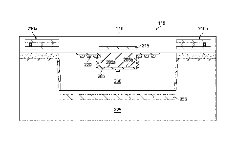
[0021] FIG. 2 illustrates a partial cross-section view of an
embodiment of the integrated photonic chip 115, as generally
shown in FIGs. 1A and 1B. In the illustrated embodiment, the
integrated photonic chip 115 includes a waveguide 205 located
on a photonic integrated circuit (PIC) substrate 210. The PIC
substrate 210 may be comprised of known materials, such as
silicon dioxide on a silicon substrate and includes one or more
interconnected metal levels 210a, 210b, formed within the
silicon dioxide layer. These features may be fabricated, using
known lithographic and deposition processes. In one embodiment,
one of the metal levels 210a, 210b of the PIC 210 may include a
backing electrode 215 that can be used to provide a
dielectrophoretic field along at least a portion of the length
of the waveguide 205. However, in other embodiments, the
backing electrode 215 is optional, and thus, may not be present
in certain embodiments. In one embodiment, the waveguide 205
may be comprised of a silicon nitride material, which can be
deposited and etched using known lithographic and deposition
processes. Silicon nitride is given as an example, but other
types of waveguides may be used, such as Gallium Arsenide,
Aluminum Gallium Arsenide, Silicon, Aluminum Oxides, Silicon
Oxy-Nitrides, Doped Silicon dioxide (Titanium, Lithium,
phosphorus, boron, etc.), or combinations thereof. The PIC
substrate 210, metal levels 210a, 210b, and waveguide 205,
along with the other components discussed below form a unique
photonic integrated circuit.
[0022] Nanoparticles 220, such as silver, gold, copper, or
combinations thereof, are located on or ("or" as used herein
and in the claims includes conjunctive and disjunctive forms,
"and/or") adjacent the waveguide 205. In one embodiment, the
6
Date Recue/Date Received 2023-07-20
concentration of the nanoparticles 220 may be greater on or
adjacent side surfaces 205a of the waveguide 205 than on an
outer surface 205b of the waveguide 205. The nanoparticles 220
extend along a sensor portion of the length of the waveguide
205. The sensor portion may extend the full length of the
waveguide 205 or only a portion of it. In one embodiment, the
waveguide 205 has cladded and uncladded portions, wherein the
uncladded portions function as the sensor portion(s). In such
embodiments, the nanoparticles 220 are located on the uncladded
portions, whereas in other embodiments, the full length of the
waveguide 205 may be cladded and the nanoparticles may be
deposited on the cladding of the waveguide 205.
[0023] The nanoparticles 220 provide improved data
collection as it relates to the test fluid or analyte in that
the nanoparticles help shape the charge transfer or plasmonic
resonance. Though metals are mentioned specifically, other
highly conductive materials that can be deposited or formed at
the nano scale may also be used. Semiconducting materials that
have been considered for use include narrow bandgap materials
such as silicon carbide, carbon, or gallium nitride as well as
narrower bandgap materials such as germanium, lead selenide,
lead telluride, Gallium Antimonide, Gallium Arsenide, Indium
Phosphide. There are additionally, several evolving
semiconductors whose nanostructure behaviors may have unique
benefits, such as the chalcoginide molybdenum disulfide (MoS2).
[0024] A second
silicon substrate 225 is bonded to the PIC
substrate 210 on the side on which the waveguide 205 is
located. The second silicon substrate 225 has a microfluidic
channel 230 formed therein, and in one embodiment, includes an
optional driving electrode 235 that works in conjunction with
the backing electrode to provide a dielectrophoretic field
along at least a portion of the length of the waveguide 205.
Known fabrication lithographic processes may be used to form
the driving electrode 235. The microfluidic channel 230
7
Date Recue/Date Received 2023-07-20
encapsulates the waveguide 205, such that the side surfaces
205a and outermost surface 205b of the waveguide 205 extend
into the microfluidic channel 225, as generally shown. The
microfluidic channel 230 provides a channel into which a test
fluid or analyte may be placed.
[0025] In those embodiments where the backing electrode 215
and the driving electrode 235 are present, they can be used to
produce an additional field to promote controlled transition of
the target molecule, such as a pathogen, to the nanostructure
surface. As seen in the illustrated embodiment, the driving
electrode 235 is located within the silicon substrate 225 and
adjacent the microfluidic channel 230 and the backing electrode
is located adjacent the waveguide 205 and within the PIC
substrate 210, as generally shown. These electrodes can be used
to apply high-frequency (3-5 MHz) voltage to the electrodes for
generating a dielectrophoretic (DEP) force within the
microfluidic channel to drive the target analytes to the
nanoparticle measuring surface.
[0026] The DEP may be used to drive biomolecules of a
specific mass and size to the measurement surface dramatically
enhancing the quantity of the target analyte which will
interact with the evanescently guided probe beam. DEP forces
can be applied to both conducting and non-conducting particles
and can be generated either by using direct current (DC) or
alternating current (AC) fields. Dielectrophoretic forces
achieves a highly accurate classification of viruses. The DEP
force is a force exerted on a suspended particle in the
presence of a non-uniform electric field. The magnitude and
direction of the force are related to the electric field
intensity, particle radius, permittivity of the particle and
suspending fluid, as well as the conductivity the particle and
suspending fluid. DEP offers the controllable, selective, and
accurate manipulation of target viruses.
8
Date Recue/Date Received 2023-07-20
[0027] As known, DEP is the movement of a particle in a non-
uniform electric field due to the interaction of the
biomolecule's dipole and spatial gradient of the electric
field. The biomolecule dipole primarily originates from two
phenomena. 1) The permanent dipole due to the orientation and
configuration of the atoms, and 2) The induced dipole resulting
from the application of an external electric field which
introduces a re-distribution of charge on the particle's
surface.
[0028] The behavior of the biomolecule can be described by
its polarizability, the measure of the ability of a material to
produce charge at the interface. Its polarizability is the
measure of the ability of the material to respond to an
electric field, which has three basic mechanisms, namely (i)
electronic polarization, (ii) atomic polarization and (iii)
orientation polarization.
[0029] Interfacial polarizability is limited since it is the
origin of the induced dipole on particles within the operating
frequencies of 10 kHz to 100 MHz. If the polarizability of the
particle is higher than that of the medium, more charges will
accumulate at the particle's side. If the polarizability of the
medium is higher than that of the particle, more charges will
accumulate at the medium's side. This non-uniform distribution
of the charges means a difference in the charge density on
either side of the particle which leads to an induced dipole
across the particle aligned with the applied electric field.
When the particle-medium system is placed in a non-uniform
electric field, the particle feels different forces at each
end. The difference in force at both ends generates a net force
in either direction depending on the polarizability of the
particle and the medium.
[0030] Common practice for application of alternating
current dielectrophoresis AC-DEP is an array of metal
electrodes embedded inside the microchannel network. Most of
9
Date Recue/Date Received 2023-07-20
the time, these internal electrodes are planar (2-D) ones
(i.e., height of the electrodes are in the order of hundred
nanometers) are fabricated within the device. AC-DEP is
advantageous due to the low operating voltage that prevents
Joule heating. Moreover, the lower applied voltages simplify
the circuitry required to generate the electric fields, making
AC-DEP focused systems compatible with integrated circuits and
suitable for battery powered hand-held devices.
[0031] Thus, DEP enhances viral detection technology,
enhancing or enriching the quantity of selective viral analytes
deposited on the measurement surface. Alternative, other
embodiments may employ variable frequency and phase selective
dielectrophoresis to separate biomolecules by size and
structure to allow selective, simultaneous, characterization
and identification of a multiplicity of analytes within the
same test structure.
[0032] FIGs. 3A-
3I illustrate partial cross-sections of
intermediate structures 300 of one embodiment of a process that
can be used to fabricate a plurality of the waveguide 205 of
the integrated photonic chip 115. FIG. 3A illustrates a silicon
substrate 305 on which a silicon dioxide layer 310 has been
grown. Also seen are a silicon nitride layer 315 and a
patterned photoresist layer 320 located on the silicon nitride
layer 315. Known processes and materials may be used to form
the illustrated intermediate structure, as hereafter discussed.
In one embodiment, the silicon substrate 305 may be a 200mm
silicon wafer doped with a P-type dopant. Depending on the
embodiment, the dopant concentration and thickness may vary. In
one embodiment, the silicon dioxide layer 310 may be formed to
a thickness of 2000nm. The thickness of the silicon nitride 315
layer that will be later patterned to form the waveguides may
also vary. In certain embodiments, the thickness may range from
about 100nm to about 200nm. In one embodiment, a dry etch may
be used to etch the unmasked portions of the silicon nitride
Date Recue/Date Received 2023-07-20
layer 315 to produce waveguides having a spacing, that may
vary, depending on design requirements. For example, in one
embodiment, the spacing between the etched waveguides may be
about 300nm.
[0033] FIG. 3B
illustrates the intermediate embodiment of
the device shown in FIG. 3A, following the patterning of the
silicon nitride 315 to form a plurality of waveguides 315a. In
one embodiment a known dry etch may be used to form the
waveguides 315a. As shown in an enlarged view 315b of one of
the waveguides 315a, the dry etch may cause the edges of the
waveguides to taper from about 00 to about 40. The tapered
edges of the waveguides 315a help to further shape the charge
transfer or plasmonic resonance. Following the dry etch, the
remaining photoresist 320 is removed from the waveguides 315a
using known processes, such as strip resist and wafer clean
processes. In some embodiments, the waveguides 315a may be
patterned into various serpentine geometric designs to increase
the interrogation or data collection lengths of the waveguide.
For example, FIG. 3C illustrates a couple of examples in which
the waveguides 315a may be patterned in a rectangular folded
configuration 315c, or a circular configuration 315d. These are
only a couple of examples, and other geometric designs are also
within the scope of this disclosure. Additionally, during the
patterning of the photoresist, the same reticle can be used to
form a tapered region 325, as seen in FIG. 3D, near an etched
facet surface 330. This narrowed tapered region 325 provides
for improved modal and optical transmission near the output end
of the waveguides. In one embodiment, a deep etch may be
conducted to define the optical facet surface 330 at the end of
the silicon nitride waveguide 315, as seen in FIG.3D. This
optional etch would be conducted to etch through the underlying
silicon oxide and then 2-3 microns into the silicon. In such
embodiments, a subsequent wet clean may be required to obtain a
smooth oxide surface.
11
Date Recue/Date Received 2023-07-20
[0034] FIG. 3E illustrates the device of FIG. 3B following
the removal of the remaining photoresist 320 and the deposition
of a nitride etch stop 335 that provides etch control for a
subsequent wet etch process. Known deposition processes may be
used to deposit the nitride etch stop 335 and may be deposited
to a thickness ranging from about 20nm to about 30nm. The
nitride etch stop 335 provides etch control for a wet etch that
is used to expose sensor portions of the waveguides, as shown
below. The nitride etch stop 335 provides etch control for a
wet etch that is used to expose sensor portions of the
waveguides, as shown below. In one embodiment the nitride etch
stop 335 remains on the waveguides 315a and serves to expand
the waveguide transmission capacity, which further enhances
data collection from the analyte.
[0035] FIG. 3F illustrates the intermediate device of FIG.
3E after the deposition of a silicon oxide layer 340, using
known deposition processes. The thickness of the silicon
dioxide layer 340 may vary, but in one embodiment, the
thickness may be about 2 microns. Also, the silicon oxide layer
340 serves as a cladding layer for at least a portion of the
waveguides 315a, as explained below.
[0036] FIG. 3G illustrates the intermediate device of FIG.
3F after the deposition and patterning of a photoresist 345 to
form a sensor opening 350 in the photoresist 345. The sensor
opening 350 exposes a region of the silicon oxide 340 to a
subsequent etch that will remove the silicon oxide from
portions of the waveguide, resulting in uncladded waveguides
315a on which the nanoparticles will be deposited and used to
collect data from the subject analyte. A known basic wet oxide
etch may then be conducted to remove the silicon oxide cladding
over targeted waveguides, which results in the intermediate
structure, as seen in FIG. 3H. As shown in FIG. 3H, a portion
of the waveguides 315a remains cladded by the silicon dioxide
340, while another portion is uncladded. These uncladded
12
Date Recue/Date Received 2023-07-20
portion serve as sensor regions that are used to collect data
regarding the subject analyte.
[0037] FIG. 31 illustrates the intermediate structure, as
seen in FIG. 3H, after the formation of the nanostructures 345
on the exposed waveguides 315a. In some embodiments, the
nanostructures 345 may have a diameter that ranges from about
70nm to about 100nm on about 140nm to 300nm pitch. However,
other ranges and pitches can be used to optimize the
performance of the device. Different deposition processes may
be used to deposit the nanostructures 345. For example, in one
embodiment, the nanostructures 345 may be deposited using an
inkjet deposition processes. In another embodiment, the
nanostructures 345 may be deposited using deep ultraviolet
(DUV) photolithography or e-beam lithography with metal
deposition liftoff. In such embodiments, the thickness of the
liftoff structures may range from about 40nm to about 80nm,
depending on the mean diameter.
[0038] FIGs. 4A-4H illustrate partial cross-sections of
intermediate structures 400 of one embodiment of a process flow
for fabricating the above-mentioned microfluidic channel 230 in
a wafer that is bonded to the wafer on which the photonic
integrated circuit and waveguide 205 are formed. Once bonded
together, the microfluidic channel 230 forms a sealed fluidic
channel around the side surfaces and outermost surface of the
waveguide(s) as seen in FIG. 2. In one embodiment, the
microfluidic channel 230 comprises two levels, a shallow etched
structure, and a deeper etched structure, as discussed below.
The shallow etch supports lateral capillary flow, while the
deeper etch structure provides vent and feed ports that are
exposed during a post back-side grind.
[0039] FIG. 4A illustrates a wafer 405, which, in one
embodiment, may be a 200mm silicon wafer that is doped with a
known P-type dopant, whose concentration and diffusion depth
may vary depending on optimized design requirements. A pad
13
Date Recue/Date Received 2023-07-20
oxide 410 is formed over the silicon wafer 405 using known
processes, such as oxidation growth or deposition processes.
The thickness of the silicon oxide layer 410 may wavy. For
example, the thickness may be about 100nm or 30nm to 50nm under
wet etch conditions. A silicon nitride layer 415 is formed over
the oxide layer 410, and in certain embodiments, its thickness
may be about 300nm. The silicon nitride layer 415 is the hard
mask feature for the shallow trench etch. The oxide layer 410
provides isolated removal of the silicon nitride 415 layer in
subsequent steps.
[0040] FIG. 4B illustrates the intermediate device of FIG.
4A following a known photoresist deposition, development, and
strip process that results in a patterned photoresist 420. The
patterned patterned photo resist 420 exposes a trench region
425 that will be subsequently etched.
[0041] FIG. 4C illustrates the intermediate device of FIG.
4B following a known hard mask etch process, which may be
either a wet or dry etch, that forms a shallow trench 430. The
etch depth may vary, but in certain embodiments, the etch depth
may be 3 to 6 microns. As seen, the etch undercuts a portion of
the oxide layer 410 and the silicon nitride layer 415. The
patterned photoresist 420, though shown, may be removed before
the etch is conducted. After the etch, the silicon nitride
layer 415 and oxide layer 410 are removed using known strip and
cleaning processes, resulting in the intermediate device of
FIG. 4D.
[0042] FIG. 4E illustrates the intermediate device of FIG.
4D following the deposition and patterning of a photoresist
layer 435 within the shallow trench 430 that will be used to
form a deeper trench. In one embodiment, a deep reactive ion
etch process, such as a BOSCH etch process, may be used to etch
a deep trench 440 to a depth of about 200 microns, resulting in
the intermediate structure shown in FIG. 4F. Following the
etch, a known strip resist ash process is conducted, flowed by
14
Date Recue/Date Received 2023-07-20
a clean process, resulting in the intermediate structure shown
in FIG. 4G that includes the shallow trench 430 and deep trench
440.
[0043] FIG. 4H illustrates the intermediate device of FIG 4G
following the removal of the photoresist and the formation of
an oxide layer 445, which, in one embodiment, may be grown to a
thickness ranging from about 75nm to about 100nm, though other
thickness may be used to optimize device performance. As
mentioned above, in those embodiments where a driving electrode
is present, an electrode may be deposited in the bottom of the
trench, or an implant may be performed to form a highly
conductive region in the exposed silicon in the bottom of the
deep trench 440.
[0044] Following the cleaning of the intermediate structure
shown in FIG. 4H, the silicon wafer 405 with the shallow trench
430 and deep trench 440 formed therein is flipped and bonded to
the photonic substrate, resulting in the general structure
shown in FIG. 2.
[0045] In one embodiment, the microfluidic channel 230 may
be fluidly coupled to a microfluidic pump 500, 505, which are
just two illustrative embodiments. FIGs 5A-53 show examples of
a couple of embodiments, but the microfluidic pumps 500, 505
may be designed as any number of serpentine configurations, as
generally illustrated by FIG. 5A and 5B. As seen in FIGs. 5A-
5B, the enhanced/modified waveguides 510, 515 and their
associated microfluidic channels 520, 525 and microfluidic
pumps 530, 535 may have several geometrical configurations that
can be used to optimize the length of the respective waveguides
510, 515 for a particular application. However, depending on
design parameters, in some embodiments, the microfluidic
channels 520 525 may not have an associated microfluidic pump.
For example, if design parameters so require, the length of the
enhanced/modified waveguide 510, 515 and microfluidic channel
may be sufficiently short so as not to require a microfluidic
Date Recue/Date Received 2023-07-20
pump. In other embodiments where design parameters require, the
enhanced/modified waveguide 510, 515 and associated
microfluidic channel 520, 525, respectively, may be longer or
more complex as seen in FIGs. 5A-53. In such embodiments, the
microfluidic pump 530, 535 is present. The analyte is
introduced into the microfluidic channel 520, 525, through the
fluid input port 540, 545. The microfluidic pumps 530, 535,
when present, can operate on a capillary principle to help draw
the fluid through the microfluidic channel and over the
waveguide so that maximum data can be obtained from the test
sample. However, in other embodiments, the microfluidic pumps
530, 535 may be mechanically driven to pump the test fluid
through the microfluidic channel. For example, the microfluidic
pump may comprise a piezoelectric material that can be used to
move the test fluid though the microfluidic channel. The length
and geometric configuration of the microfluidic channels 530,
535 may vary and will be depend on design parameters and system
requirements. In the illustrated embodiments, the microfluidic
channels 520, 525, and microfluidic pumps 530, 535 have a
general serpentine configuration, but as just mentioned, other
geometric configurations are within the scope of this
disclosure. These folded types of pathways can be used to
increase the data collection length of the device, while
keeping the device exceptionally small for a compact form.
Known photolithographic processes and materials may be used to
fabricate the microfluidics channel.
[0046] FIG. 6
illustrates a general block diagram layout of
one embodiment of the integrated photonic chip 115. This
embodiment comprises a photonic tuning and control circuit 600
that includes an interferometer for signal extraction and a
stabilized optical source, as discussed below, a configuration
management circuit, digital processor core, memory, a USE data
interface, a power source, and a known wireless interfacefor
quick and easy transmission of the data. The analyte enters the
16
Date Recue/Date Received 2023-07-20
microfluidic channel 605 through the input port 615. As the
fluid travel through the microfluidic channel 605, quantitative
or qualitative data is produced by the interactions between the
evanescent field of the light in the waveguide 610, the
nanoparticles, and the analyte in the fluid. The fluid travels
through the microfluidic channel and exits through a vent port
620 and back into the fluid channel of the test strip, as
discussed above. Thus, this disclosure presents a micro-sized
photonic integrated circuit that provides accurate fluidic
analysis with rapid results.
[0047] FIG. 7 illustrates a general schematic overview
configuration of one embodiment of the waveguide enhanced
analyte detection apparatus. In this embodiment, the photonic
integration is combined with microfluidics and additive
manufacturing to quickly implement a compact Raman Spectroscopy
based system to provide rapid detection and identification of
pathogens or other biochemical or non-biochemical substances.
[0048] As mentioned above, one embodiment of this disclosure
uses Raman spectroscopy, though other similar types of
spectrometers may also be used. Raman spectroscopy is a known
technique in which incident laser light is inelastically
scattered from a sample and shifted in frequency by the energy
of its characteristic molecular vibrations. The Raman spectrum
provides high informational content on the chemical structure
of the probed substances, which makes this method an ideal tool
for the identification of viruses and bacteria, illicit drugs,
pharmaceutical and drug manufacturing monitoring/validation or
cancer cell detection and identification. However, unlike
focusing the Raman beam on a single point on a surface
containing a targeted subject matter, as done in conventional
systems, the embodiments of this disclosure provide for a
structure that collects data along the length of the waveguide
or waveguides, thereby greatly enhancing the quantity and
accuracy of the data.
17
Date Recue/Date Received 2023-07-20
[0049] The test analyte or fluid is injected into the
microfluidic channel that provides confinement of the analyte
under test. This confinement ensures the greatest overlap of
the analyte with the probe beam. Further, it provides intimate
and strong interaction of the molecules with nanostructures
along the walls of the microfluidic channel, which provides
enhanced Raman Signal strength.
[0050] The application of Surface-enhanced Raman
spectroscopy (SERS), to improve signal strength is a
modification of Raman spectroscopy. It has been demonstrated as
a very capable approach to identify biomolecules, such as a
bacterium or viruses. It is based on the enhancement of the
Raman scattering signal of certain molecules when they are
adsorbed or placed in the proximity of appropriate metallic
nanostructures, usually noble metals, such as silver, gold, or
copper. It has been shown that the SERS approach can yield
enhancement factors as large as 1014-1015, leading to Raman
scattering cross sections larger than those of fluorescent
organic dyes or other reagents used in modern test sets or
detection panels.
[0051] The embodiments of this discloser detect the Raman
spectrum from the SERS interactions using a detector coupled
with an interferometer, such as a Michaelson interferometer, as
generally shown in FIG. 8, which schematically illustrates an
embodiment of an interferometer, such as a Michaelson
Interferometer, and a stabilized optical source that form
portions of the photonic integrated circuit of the integrated
photonic chip 115. This unique approach generates an
interferogram that contains the frequency dependent information
modulated in a time domain as a function of the phase
propagation length variation in one arm of the spectrometer.
The system will then perform a Fourier-transform to extract the
detailed Raman spectrum used to detect and identify viruses
present in the sample.
18
Date Recue/Date Received 2023-07-20
[0052] The photonic integrated circuit Fourier-transform
(FT) spectrometer generates its output spectrum by modulating
the radiation in the time domain through interference, which
then undergoes a Fourier transformation. The detection and
identification of pathogens is insured by the ability to
integrate 6 elements into a relatively small area, such as the
illustrated test chip, by leveraging semiconductor
manufacturing and packaging techniques. These include: 1)the
stabilized narrow band optical source to provide a controllable
Raman Probe; 2) The evanescently coupled low index contrast
waveguides providing controlled overlap of the modal energy
traveling external to the waveguide and the metallic
nanostructures which provide the photonic enhancement of the
Raman Scattering; 3) Formation of nano structures between and
on the waveguides providing a controlled surface region for
characterization of a pathogen; 4)The integration of electrodes
which allow controlled enrichment of the target pathogen at the
metallic nanostructure surface; 5) The Integration of
microfluidic structures to confine the sample volume relative
to the waveguides and enrichment structures; 6)The ability to
integrate a small Fourier transform spectrometer.
[0053] The interference between the signal propagating along
the phase modulated arm, and the non- phase modulated arm are
reflected to the coupler where the variation in phase causes an
amplitude change. When this recorded, time-based amplitude
information is recorded against the driving voltage or
resulting effective path length variation in the modulated arm,
it is called an interferogram, I(xeff). This Interferogram
represents a modulated radiation signal as a function of the
change in effective path length between the two arms of the
interferometer. In the interferometric photonic circuit, the
analog signal is recorded at a photodetector, which encodes the
wavelength or the wave number information of the encoded Raman
spectrum. A Fourier-transform routine is then performed on the
19
Date Recue/Date Received 2023-07-20
interferogram to recover the Raman spectrum. An advantage of
this system is the photonic integrated circuit, stabilized
optical source. In one embodiment, a resonant cavity is used to
define the initial gain distribution which is stabilized
relative to the external cavity and composed of a Bragg mirror
and phase tuner. This approach allows the control over the
phase and frequency content of the signal being reinjected for
injection locking of the resonant gain stage.
[0054] In the
operation of one embodiment, the test fluid is
placed into the microfluidic channel through an input port. A
stabilized optical source, such as a laser, is then guided
within the waveguide that is formed along at least a partial
length of the microfluidic channel. Since the region where the
channel and optical waveguide is relatively long, and the
evanescently guided region around or between the waveguide will
interact with a larger number of target analytes, an increase
can be obtained through the summation of the interactions,
thereby enhancing the accuracy of the test. At the end of the
sensor region, the optical signal is then input into an
integrated spectrometer that measures properties of light over
the specific portion of the electromagnetic spectrum associated
with the subject molecule or pathogen. These spectrometers may
take the form of a wide range of integrated structures, from
resonator coupled detectors to scanned structures such as Mach-
Zehnder and Michaelson interferometers. The approach shown
details the use of an integrated Michaelson Interferometer,
whereby the phase induced propagation variation in one arm,
versus the fixed length of a reference arm, introduces an
interference pattern interferogram, which is then transmitted
to an internal or external processor. This is then, by means of
a Fast Fourier Transform (FFT), converted to the spectrum from
which a unique fingerprint, consisting of unique peak
positions, widths, and shapes, can be processed by a comparator
to obtain the final data set. The final data set can be
Date Recue/Date Received 2023-07-20
transmitted to a detectable format, such as a visual signal or
alphanumeric readout.
[0055] FIG. 9, schematically illustrates how, in one
embodiment, the interferometer and stabilized optical source
are optically coupled to the waveguide, which may have an
overall length, including the fluid input and vent ports
between about 3mm to about 4 mm and where the line width source
ranges from about 0.5mW to about 5mW.
[0056] FIG. 10 illustrates an embodiment of a general
fabrication process flow that can be used to fabricate the test
chip.
[0057] The unique benefits of the various embodiments of the
test strip detection and identification system include the
ability to confine solutions that contain viral materials to a
microchannel. This confinement provides improved interaction
between the probe light beam and target materials. The
embodiments herein provide a compact analytical system having
multiple orders of magnitude improvement in sensitivity over
any other approach, for example, it is believed that 14 to 15
orders of magnitude increase in signal sensitivity that results
from application of metallic nano structures along the walls of
the microchannel is possible. The forced interaction with the
multiple surfaces of the nanoparticles within the microchannel
increases the overall interaction length and accumulated signal
strength. Other advantages provided by the embodiments herein,
include low-cost generation, coupling, transmission, processing
and detection of the Raman spectrums, application of
microchannel integration technologies to support the formation
of the localized metallic nanostructures within the channels
and their integration with the photonic integrated circuits,
and the supporting elements to control injection of the probe
light beam into the microchannel. This system allows guidance
of the probe beam in a controlled manner through the
microchannel and re-coupling of the probe beam back into the
21
Date Recue/Date Received 2023-07-20
photonic circuit for processing and spectrum extraction. The
embodiments herein also provide packaging of the sensor into a
useable vehicle to allow isolated, real-time single point
testing without putting additional persons at risk.
[0058] Embodiments disclosed herein comprise:
[0059] In one embodiment a photonic integrated chip is
disclosed. In this embodiment, the photonic integrated chip
comprises an optical waveguide located on a photonic circuit
substrate comprising a photonic circuit. The optical waveguide
is optically coupled to the photonic circuit. A microfluidic
channel is in a silicon substrate and electrically and
optically coupled to the photonic circuit substrate, wherein
the microfluidic channel is positioned over the optical
waveguide. Side surfaces and an outermost surface of the
optical waveguide extend into the microfluidic channel. The
microfluidic channel extends along a length of the optical
waveguide. Nanoparticles located on or adjacent the optical
waveguide is located within the microfluidic channel.
[0060] Another embodiment is directed to a test strip. This
embodiment comprises a photonic integrated chip. The photonic
integrated chip comprises an optical waveguide located on a
photonic circuit substrate comprising a photonic circuit. The
optical waveguide is optically coupled to the photonic circuit.
A microfluidic channel is in a silicon substrate and attached
to the photonic circuit substrate, wherein the microfluidic
channel is positioned over the optical waveguide. Side surfaces
and an outermost surface of the optical waveguide extend into
the microfluidic channel and the microfluidic channel extends
along a length of the optical waveguide. Nanoparticles located
on or adjacent the optical waveguide located within the
microfluidic channel. The integrated photonic chip is located
on and a fluid collection strip and adjacent one of its ends.
The fluid collection strip has a fluid channel formed therein
and a fluid input port fluidly connected to the fluid channel.
22
Date Recue/Date Received 2023-07-20
The fluid input port is located adjacent an opposing end of the
fluid collection strip, and a vent port is fluidly connected to
the fluid input port of the integrated photonic chip to allow a
flow of fluid from the fluid channel and into the microfluidic
channel of the integrate photonic chip.
[0061] Element 1: further comprising, a driving electrode
and a backing electrode, wherein the driving electrode is in
the silicon substrate and the driving electrode is in the
photonic circuit substrate, the optical waveguide located
between the driving electrode and the backing electrode
positioned over the optical waveguide.
[0062] Element 2: wherein the photonic integrated circuit
comprises a photonic tuning and control circuit, a
configuration management circuit, a digital processor core, a
memory circuit, a digital interface, and a Bluetooth interface.
[0063] Element 3: further comprising a fluid input port and
a fluid vent port located on opposing ends of the microfluidic
channel, the microfluidic channel forming a fluid path between
the fluid input port and the fluid vent port.
[0064] Element 4: further comprising an optical stabilizer
and an interferometer comprising a modulated path length for an
input signal and a fixed path length for a phase modulated
output signal.
[0065] Element 5: wherein the optical stabilizer comprises
an optical gain circuit, and a phase modulation optical circuit
coupled to a Bragg mirror.
[0066] Element 6: wherein a concentration of the
nanoparticles is greater on or adjacent the side surfaces than
on the outermost surface.
[0067] Element 7: wherein a portion of the waveguide is
uncladded, and the nanoparticles are on or adjacent the
uncladded waveguide.
[0068] Element 8: wherein the waveguide has a serpentine
configuration.
23
Date Recue/Date Received 2023-07-20
[0069] Element 9: further comprising a microfluidic pump
fluidly connected to the microfluidic channel.
[0070] Element 10: wherein the integrated photonic chip
further comprises, a driving electrode and a backing electrode,
wherein the driving electrode is in the silicon substrate and
the driving electrode is in the photonic circuit substrate, the
optical waveguide located between the driving electrode and the
backing electrode positioned over the optical waveguide.
[0071] Element 11: wherein the photonic integrated circuit
comprises a photonic tuning and control circuit, a
configuration management circuit, a digital processor core, a
memory circuit, a digital interface, and a Bluetooth interface.
[0072] Element 12: further comprising an optical stabilizer
and an interferometer comprising a modulated path length for an
input signal and a fixed path length for a phase modulated
output signal.
[0073] Element 13: wherein the optical stabilizer comprises
an optical gain circuit, and a phase modulation circuit optical
coupled to a Bragg mirror.
[0074] Element 14: wherein a concentration of the
nanoparticles is greater on or adjacent the side surfaces than
on the outermost surface.
[0075] Element 15: wherein a portion of the waveguide is
uncladded, and the nanoparticles are located on or adjacent the
uncladded waveguide.
[0076] Element 16: wherein the waveguide has a serpentine
configuration.
[0077] Element 17: wherein a portion of the waveguide is
uncladded, and the nanoparticles are located on or adjacent the
uncladded waveguide.
[0078] Element 18: wherein the fluid collection strip
comprises a top film on which the integrated photonic chip is
located, a bottom film, and a spacer film, the top and bottom
24
Date Recue/Date Received 2023-07-20
films and the space film being attached together to form the
fluid channel.
[0079] Although the present invention has been described in
detail, those skilled in the art should understand that they
can make various changes, substitutions, and alterations herein
without departing from the spirit and scope of the invention in
its broadest form.
Date Recue/Date Received 2023-07-20