Note: Descriptions are shown in the official language in which they were submitted.
WO 2021/215939
PCT/NZ2021/050067
METHOD TO APPLY COLOR COATINGS ON ALLOYS
BACKGROUND
[0om] Various methods have been developed to coat colored anodized
films on light metal alloys. In many cases, the exact coloration mechanism is
not defined. However, it is generally understood that total internal
reflection
between the clear anodizing, the reflective substrate, and the inorganic
deposits generates the change i luminance (L*), whereas the chrominance
and hue (a*, b*) are created by destructive interference between the incoming
and reflected light. In the case of organic coatings, coloration is often a
direct
consequence of the selected organic molecule.
[0002] In U.S. patent 4,251,330 ('330 patent), a mechanism to
intensely
color anodized aluminum or aluminum alloys is disclosed. In this patent, the
substrate is direct current (DC) anodized to a thickness of 15 microns in a
mostly sulfuric acid bath. The pores are widened in a mostly phosphoric bath
using mostly alternating current (AC) anodizing. Coloration is provided by
depositing mostly nickel from an acidic nickel sulfate, magnesium sulfate, and
boric acid bath using AC. A variety of colors from purples, to blues, to
greens
is developed from destructive interference.
[0003] AC phosphoric anodizing was thought to be beneficial due
to more
uniform widening of the pores, while AC deposition resulted in a difference in
deposition in the modified (widened) pores against the original narrow pores.
The process disclosed in the '330 patent requires two baths to produce the
pore structure necessary to color the surface, and thus, is less controlled.
[0004] Furthermore, the residual acid from the widening and
deposition
process leads to mudding of the colors, which requires a further
neutralization
step.
[0005] Patent EP018247981 discloses a direct coloration process
using
nickel sulfate in a sulfuric anodizing structure using AC deposition.
[0006] US patent 5,064,512 discloses a process for dyeing a
sulfuric
1
CA 03175978 2022- 10- 17
WO 2021/215939
PCT/NZ2021/050067
anodized substrate using organic tin salts on sulfuric anodized substrates
using AC or AC superimposed on DC coloration. This patent particularly
discusses the need to stabilize the tin content of the bath and increase the
throwing power of
the solution. The process requires a complex preparation of the tin containing
coloration bath and close monitoring of the tin content to achieve the desired
results.
[0007] Patent WO 01/18281 discloses a method for producing
predominantly black anodized coatings by anodizing an aluminum or
aluminum alloy substrate in a sulfuric bath to produce an oxide layer from 8-
microns thick, modifying the pore structure in a predominantly phosphoric
bath using reduced voltage AC or DC anodizing such that a large percentage
of the pores become unable to participate in the coloration process, and
coloring the anodized layer using a bath containing inorganic salts and a
15 UNICOLO modified AC deposition regime. This process is largely a
modification of the process disclosed in the '330 patent, discussed above,
but relies on a different pore modification process. In each of the above
cases, the coloration derives from modifying a sulfuric anodizing structure
using a phosphoric process and then coloring the part using an inorganic
bath.
SUMMARY
[0008] According to aspects illustrated herein, there is
provided a method
for coloring a light metal alloy. One disclosed feature of the embodiments is
a method comprising anodizing a substrate in an anodizing bath comprising
phosphoric acid, at a constant temperature and a constant voltage for a first
time period to develop an anodizing layer that includes a barrier layer,
reducing the constant voltage applied to the anodizing bath for a second
time period to change a thickness of the barrier layer and change a width of
pores in the anodizing layer, plating the substrate in a plating bath at a
first
2
CA 03175978 2022- 10- 17
WO 2021/215939
PCT/NZ2021/050067
current that is increased over a third time period in accordance with a
current
profile of the plating bath, and plating the substrate in the plating bath at
a
second current for a fourth time period.
[0009] One disclosed feature of the embodiments is a method
comprising
anodizing an aluminum alloy substrate in an anodizing bath comprising
phosphoric acid, at a constant temperature and a constant voltage for a first
time period to develop an anodizing layer that includes a barrier layer to be
between 2 and 10 microns thick reducing the constant voltage applied to the
anodizing bath for a second time period to change (i) a thickness of the
barrier layer, located between the substrate and anodizing pores, and (ii) a
width of
pores in the anodizing layer, plating the aluminum alloy substrate in a
plating
bath at a first current that is increased over a third time period in
accordance
with a direct current (DC) plating current profile of the plating bath,
plating the
aluminum alloy substrate in the plating bath at a second current for a fourth
time period to partially fill the pores in the anodizing layer with metal
nanorods, and seal the pores of the anodizing layer to form a sealing layer.
In one embodiment the step of sealing the pores leaves an airgap between
the metal nanorods and the sealing layer.
[ow 0] One disclosed feature of the embodiments is a method
comprising
pre-treating an aluminum alloy substrate, activating the aluminum alloy
substrate, anodizing the aluminum alloy substrate in an anodizing bath
comprising phosphoric acid, at a constant temperature and a constant voltage
for a first time period to develop an anodizing layer, reducing the constant
voltage applied to the anodizing bath for a second time period to change a
thickness of the barrier layer and change a width of pores in the anodizing
layer, rinsing the aluminum alloy substrate to further reduce the thickness of
the barrier layer, plating the aluminum alloy substrate in a plating bath via
multiple plating stages to deposit a coloring metal nanorods into the pores of
the anodizing layer, and sealing the pores of the anodizing layer while
leaving an air gap above the metal nanorods..
3
CA 03175978 2022- 10- 17
WO 2021/215939
PCT/NZ2021/050067
BRIEF DESCRIPTION OF THE DRAWINGS
[owl] FIG. 1 illustrates a flow chart of an example method for
producing a
thin colored coating;
[0012] FIG. 2 illustrates an example sulfuric anodized substrate;
[ow 3] FIG. 3 illustrates an example phosphoric anodized
substrate of the
present disclosure;
[ow 4] FIG. 4 is a surface electron microscope (SEM) image of an
example
phosphoric anodized structure of the present disclosure;
[0015] FIG. 5 is a SEM image of an example cross-section of an anodized
colored substrate of the present disclosure;
[0016] FIG. 6 is a SEM image of an example close up image of a
cross- section
[ow 7] FIG 7 illustrates an example ultraviolet imaging
spectrograph (UVIS)
spectrum for a colored hybrid coating on 6061 aluminum of the present
disclosure;
[ow 8] FIG. 8 illustrates an example graph showing a
relationship
between the anodizing charge passed, the plating amp minutes, and the
color in a process of the present disclosure;
[ow 9] FIG. 9 illustrates an example diagram of the color generating
mechanism of the present disclosure;
[0020] FIG. 10 illustrates an example graph showing the
relationship
between the average roughness of the substrate and the gloss of a coating
of the present disclosure;
[0021] FIG. 11 illustrates an example graph showing the maximum
achievable anodizing layer thickness for several phosphoric acid
concentrations
of the present disclosure; and
[0022] FIG. 12 is a set of example images and a table showing
the effects
of barrier layer thinning and the temperature on the coating color of the
present disclosure.
4
CA 03175978 2022- 10- 17
WO 2021/215939
PCT/NZ2021/050067
[0023] FIG 13 is a cross section diagram of a coating according
to one
aspect of the invention showing the air gap to retain surface color
DETAILED DESCRIPTION
[0024] Examples described herein provide a process to develop a thin
colored coating on an aluminum or light metal alloy. As discussed above,
various methods have been developed to coat alloys. Anodic oxide films on
aluminum (including aluminum alloys) can be colored using both organic
and inorganic coloring agents. The coloring occurs through deposition of
organic or inorganic material in the pores using, generally, alternating
current
between the anodized surface and a counter electrode, while immersed in a
bath containing the appropriate inorganic salt or combination of inorganic
salts and organic molecules.
[0025] Previous methods have many drawbacks or may be
inefficient.
The present disclosure provides a method that can anodize and color
aluminum, and other light metal surfaces, using a two-step process
involving phosphoric anodizing and direct metal deposition. Thus, the
process of the present disclosure may be more efficient and more
environmentally friendly due to the use of less energy, fewer volatile organic
compounds, and less waste.
[0026] In one embodiment, the process may incorporate one or
more of
the following steps: degreasing an alloy substrate, electropolishing the
substrate, activating the surface, anodizing a film of between 2 and 10
microns on the substrate in an anodizing bath comprising substantially
phosphoric acid at a desired temperature and following a desired voltage-
current profile, electro- depositing a metal into the anodizing pores at a
desired temperature and following a desired current profile, and sealing the
pores with a transparent medium. The total average thickness of the hybrid
coating may be around 2 to 15 microns.
[0027] FIG. 1 illustrates an example method 1 00 for producing a thin film
5
CA 03175978 2022- 10- 17
WO 2021/215939
PCT/NZ2021/050067
colored coating of the present disclosure. In one embodiment, the method
100 may be performed by various equipment or tools in a processing facility
under the control of a processor or controller.
[0028] At block 102, the method 100 begins. At block 104, the
method
100 may pre-treat a substrate. In one embodiment, the substrate may
comprise aluminum or any alloy of aluminum.
[0029] The pre-treatment may include degreasing the substrate in
an
alkaline bath, roughening the substrate in a solution of polyethylene glycol,
sulfuric acid and hydrofluoric acid, or other similar solution, and etching
the
substrate in a nitric acid solution. An example of such a pre-treatment may be
a commercial aluminum surface pretreatment called Probright AL. The
solution to roughen the substrate may clean the substrate surfaces as it
etches.
[0030] One example of the pre-treatment may include the
substrate first
being treated by degreasing in a commercial solution such as Activax,
commercially available from MacDermid, Inc. The degreasing step may be
followed by rinsing. Rinsing of the substrate prior to anodizing may have the
effect of eliminating impurities on the surface, which may cause imperfections
in a thin anodized layer.
[0031] In one embodiment, the pretreatment may include electropolishing the
substrate in a bath selected from the following ranges: 70-85% of H3PO4, 2-4
of HF, 6-9% of H2SO4, and 5-20% of glycerol. The electropolishing bath may
be held at a temperature of between 70 and 80 Celsius ( C) at a voltage (V)
of approximately 12V. The electropolishing bath may include a Pb counter
electrode. The electropolishing step creates a uniform surface of the
substrate with a low average roughness (Ra), which contributes to achieving
a glossy colored coating. The electro- polished substrate may then be rinsed
in de-ionized (DI) water prior to the activating and anodizing steps,
discussed
below.
[0032] The average surface roughness, Ra, of the aluminum alloy substrate
6
CA 03175978 2022- 10- 17
WO 2021/215939
PCT/NZ2021/050067
directly relates to the apparent gloss of the colored coating. In one
embodiment, the Ra of the substrate prior to anodizing may be between 1.8 and
4 to achieve a matte surface. In one embodiment, the Ra may be approximately
2.
[0033] In one embodiment, the Ra of the substrate prior to anodizing may be
between 0.4 and 1.8 to achieve a semi-gloss surface. In one embodiment, the
Ra may be between approximately 0.8 and 1.2.
[0034] In one embodiment, the Ra of the substrate prior to
anodizing may be
between 0 and 0.4 to achieve a gloss finish. In one embodiment, the Ra may be
less than approximately 0.2.
[0035] At block 106, the method 100 may activate the substrate.
The
substrate may be activated prior to anodizing. The activation step may
provide some benefits on certain alloys. One example of the activation step
may include activating the surface in a bath comprising 40% by volume
HNO3 and between 1 and 10 milliliters per liter (mL/L) of HF. In one
embodiment, between 20% and 50% by volume of HNO3 may also be used.
The bath may be maintained at a temperature between 20 C-25 C with the
substrate being immersed and agitated about once per second for between 20
and 40 seconds.
[0036] At block 108, the method 100 places the substrate in an anodizing
bath comprising phosphoric acid and additives or solvents that support the
desired anodizing voltage and thus determine the pore structure which
determines the resulting coating color. The bath may include at least
phosphoric acid and sulfuric acid for an initial period to produce a thin
anodized layer. In one embodiment, the temperature, electrical parameters,
and bath composition contains a uniform high-density distribution of thin
walled pores between 50 and 160 nanometers (nm) in diameter, as shown in
FIG. 5, and discussed in further detail below.
[0037] The anodizing bath contains principally phosphoric acid
with small
amounts of sulfuric and oxalic acids. A bath composition is selected from
7
CA 03175978 2022- 10- 17
WO 2021/215939
PCT/NZ2021/050067
the range of H3PO4 (40-600 ml per liter (m1/1)), H2SO4 (0-1 5m1/I), and
HOOCCOOH (1 -10 grams per liter (g/L)). In one embodiment, the
concentration of H3PO4 may be approximately 150 m1/1, the concentration of
H2SO4 may be approximately 0.6m1/I, and the concentration of
HOOCCOOH may be approximately 1g/I and the solvent is DI water.
[0038] In some embodiments, other additives may be added to
attain a
desired pore structure of the anodized layer. Examples of other additives
may include small amounts of copper sulfate, a chelating agent, and the
like, discussed in further detail below.
[0039] For any given phosphoric acid concentration in the anodizing bath,
there may be a maximum anodizing thickness achievable due to the pore
widening effect of the phosphoric acid. In one embodiment, the maximum
anodizing thickness may be about 6 microns. While increasing the
phosphoric acid concentration increases the conductivity of the anodizing
bath, thus increasing the current density for a fixed anodizing voltage,
increased phosphoric acid concentration may also increase the pore
widening and film dissolution, giving rise to the aforementioned limit on
thickness for the anodized film. The addition of a short chain alcohol in the
range 0¨ 15 weight per cent (wt%), or approximately 10 wt%, has been
shown to cool the growing pore structure and to reduce the surface
dissolution of the porous anodized structure by the anodizing bath. The
addition of ethylene glycol in the range of 0 ¨ 80 wt%, or approximately 50
wt%, may increase the viscosity of the electrolyte, thereby reducing the rate
of pore widening at the cost of lowering the growth rate of the porous
anodized film. Low volumes of phosphoric acid may allow thicker anodizing
layers. This may improve the coating mechanical performance, but requires
longer anodizing times due to slower film growth.
[0040] The thickness of the barrier layer and pore structure has
been
shown to be factors in determining the coating color as described in the
examples below. The thickness of the barrier layer is proportional to the
8
CA 03175978 2022- 10- 17
WO 2021/215939
PCT/NZ2021/050067
anodizing voltage. However, the pore width is also proportional to the
anodizing voltages. In many instances, the requirements of a thick barrier
layer with narrower pores may play an important role in creating a functional
colored coating. The addition of polyethylene glycol, or similar organics
which increase the anodizing solution viscosity, in the range of 10-50 wt%,
has been shown to allow higher anodizing voltages, which develop thicker
barrier layers while keeping the pore size low or smaller than previous
methods. The replacement of up to 50% of the H3PO4 with either NaH2PO4
or LiH2PO4 lowers the acidity and thus both the pore wall and barrier layer
dissolution, allowing higher voltages, thicker barrier layers and narrower
pore mouths. The thicker barrier layer so developed may be changed by
thinning as described below to develop the correct or desired color for the
coating.
[0041] At block 110, the method 100 anodizes the substrate at a
voltage
and a temperature for a time to develop a pore structure. For example, the
substrate may be placed in an anodizing bath. The anodizing bath may be
operated at a constant temperature between 5 C-40 C, or between 27 C
and 31 C. The temperature of the bath may be regulated to develop the
optimum pore structure. In one embodiment, the temperature may be
maintained within 2 C. In one embodiment, the temperature may be
maintained within 1 C. In one embodiment, the temperature may be
maintained within 0.5 C.
[0042] In one embodiment, a constant voltage may be applied to
the
anodizing bath. In one embodiment, the voltage may be between 60V and
280V and have a maximum current density of 2 amperes per square
decimeter (A/dm2) to provide an optimum pore distribution, density, and
structure, as further described below.
[0043] In one embodiment, the initial voltage may be between 60
and 80
volts and the anodizing time period may be between 10 and 40 minutes. In
one embodiment, voltage may be approximately 65V and the time period
may be approximately 20 minutes.
9
CA 03175978 2022- 10- 17
WO 2021/215939
PCT/NZ2021/050067
[0044] The thickness of the anodized film/layer in the present
disclosure
may be developed or grown to be between 2 and 10 microns. However, the
thickness may also be between 2 and 8 microns. In one embodiment, the
thickness may be between 4 and 5 microns. Anodizing for 20 minutes at the
above described conditions results in an anodized film of about 6 microns
thick. In one embodiment, pulsed DC anodizing may be adopted. In one
embodiment, the hue of the coating may be dependent on the thickness of the
anodizing layer (also referred to herein as a barrier layer), as described
below. For anodizing baths composed of an acid or a mixture of acids, the
structure of the anodized layer may be generalized as comprising a compact
barrier layer immediately adjacent to the alloy substrate, and a porous layer
above the barrier wherein pores extend substantially perpendicularly from the
barrier layer to the surface. At block 112, the method 100 may optionally
change the voltage and temperature of the anodizing bath for an additional
time period to develop a fine structure. For example, the thickness of the
barrier layer and the width of the pores may be changed (e.g., reducing
thickness of the barrier layer while increasing the width of the pores or
increasing the thickness of the barrier layer while decreasing the width of
the
pores).
[0045] In one embodiment, the anodizing voltage may be reduced following
a voltage profile to thin the barrier layer, and increase the light absorption
and
thus darken the color, as shown in FIG. 5. As described below, the width of
the anodizing pores and the thickness of the barrier layer are produced as a
function of the anodizing voltage and the dissolution power of the anodizing
electrolyte(s). In one embodiment, the anodizing voltage is reduced by 50%
and anodizing is continued for between 2 and 10 minutes, or for
approximately 5 minutes in one embodiment.
[0046] In one embodiment, the anodizing voltage is similarly
reduced by
50% for between 2 and 10 minutes, or for approximately 5 minutes in one
embodiment. Then the anodizing voltage is reduced by 50% again for a further
period of between 2 and 10 minutes, or for approximately 5 minutes in one
CA 03175978 2022- 10- 17
WO 2021/215939
PCT/NZ2021/050067
embodiment.
[0047] In one embodiment, the anodizing voltage is ramped from
the initial
voltage to 15% of the initial voltage over a period of between 2 and 20
minutes, between 5 and 15 minutes, or between 8 and 12 minutes. It will be
apparent to those skilled in the art that further reductions are possible with
different voltages and time periods to create different pore structures.
[0048] At block 114, the method 100 optionally chemically rinses
the substrate.
For example, the substrate may be rinsed in a solution to further thin the
barrier
layer and prepare the substrate for plating the coloring metal. In one
embodiment, the rinsing may thin the barrier layer by partially dissolving the
anodizing endcaps. In one embodiment, the solution may be a bath comprising
between 0.5-5 mL/L HF.
[0049] The anodized substrate to be processed may be immersed in
the
rinse bath for approximately 30 seconds, while being agitated about once
per second. It will be apparent to those skilled in the art that other
chemical
baths and methods may be adopted to chemically thin the barrier layer.
[0050] At block 116, the method 100 places the substrate in a
bath
containing metal sulphates or cyanides to be plated following a current
profile
and develop metal nanorods at the base of the pores. In one embodiment,
the nickel sulphate may, for example, be a source of metal for producing the
colored coating, referred hereafter as a coloring metal. The coloring metal
may be plated into the pores of the anodized layer of the substrate in an
electro deposition bath following a plating current profile for a
predetermined
period. For example, a coloring electrodeposited coating may be applied to
the anodizing film from a bath selected from a range of possible baths. The
electrical parameters pertaining to the metallic coloring deposition are
controlled by a first plating stage and a second plating stage. The first
plating
stage may include a first plating current that may be applied for a first
plating
period. The second plating stage may include a second plating current that
may be applied for a second plating period.
[0051] In an alternative embodiment the coloring metal may be
any pure
11
CA 03175978 2022- 10- 17
WO 2021/215939
PCT/NZ2021/050067
metal including without limitation, silver, gold, copper, cobalt, tin or a
metallic
alloy including without limitation, zinc-nickel, nickel-phosphorous, cobalt-
phosphorous or the like.
[0052] In one embodiment, the substrate may be optionally soaked
in
the metallic coloring solution for a period of between 0 and 6 minutes prior
to
the plating. In one embodiment, the substrate may be soaked for
approximately 3 minutes. Soaking the substrate in the metallic coloring
solution may allow the metal ions to fully diffuse into the pores and may
allow
any residual anodizing solution to be rinsed from the pores.
[0053] In one embodiment, the plating process to develop metal nanorods at
the base of the pores and color the substrate may be performed in multiple
stages. The first color deposition stage may proceed for the first plating
period, during which the first DC plating current profile is set at a
percentage
of the second plating current, where the second plating current is set at a
percentage of the nominal plating current for a chosen bath composition. The
first plating current may be selected to be between 10% and 50% of the
second plating current. In one embodiment, the first plating current may be
selected to be approximately 33% of the second plating current.
[0054] The second plating current may be selected to be between
1%
and 20% of the nominal plating current for a chosen bath composition. In
one embodiment, the second plating current may be selected to be
approximately 10% of the nominal plating current for a chosen bath
composition. The first plating current profile may ensure the nucleation of
the coloring metal at the bottom of the anodized porous structure. The
nominal plating current may be defined by the Technical Data Sheet (TDS)
provided by a formulator for a plating bath.
[0055] For example, the DC plating current for the semi-bright
nickel bath
referred to herein may be between 2 and 4 A/dm2. In one embodiment, the
nominal plating current may be 3 A/dm2 for the bath described herein. The
first current profile may be imposed such that the plating current is ramped
from 0 to the selected current over 2 to 8 minutes. In one embodiment, the
12
CA 03175978 2022- 10- 17
WO 2021/215939
PCT/NZ2021/050067
current may be ramped up over 3 minutes.
[0056] The second plating period may be sufficient to grow the
metal
nanorods to partially fill the anodizing pores, without reaching the top of
any
of the anodizing pores. In one embodiment, the second plating period is
dependent on the thickness of the anodized film and the required luminance
as further described below.
[0057] A sufficient time may be defined by the function below.
In one
embodiment, between 2 and 10 minutes may be sufficient time to produce a
black surface in a semi-bright nickel bath with a second plating current of
10% of the nominal plating current in an anodizing layer of 6 microns. The
plating rate for this reduced current has been shown to be between 0.05 and
0.5 times that for the bath under normal operating conditions. Thus, the
plating period during which the plating current is applied may be approximated
by Equation (1) below:
a * fill fraction
Equation (1) t =
n *rate factor'
where 't' is the plating period time in minutes, 'd' is the thickness of the
anodized layer in microns, fill fraction is the desired average fill (i.e. the
length of
the metal nanorods as a percentage of the anodizing layer thickness) to
produce a
defined color, 'n' is the plating rate under normal bath operating conditions
for
the first electrodeposition bath in microns/minute, and rate factor is between
0.05 and 0.5 depending on the percentage reduction of the current, the normal
plating efficiency of the selected plating bath, and the plating rate change
versus current for this bath.
[0058] In one embodiment, pulsed DC or pulse/pulse reverse DC
plating
may be adopted. The pulse plating may result in uniform nanorod lengths by
both limiting hydrogen evolution and changing the metal nucleation at the
base of the anodizing pores.
[0059] In one embodiment, the first electro-deposited layer may be
13
CA 03175978 2022- 10- 17
WO 2021/215939
PCT/NZ2021/050067
deposited from a semi-bright nickel bath such as Chemipure/Niflow,
commercially available from CMP India. In another embodiment, the first
electro-deposited layer may be deposited from a copper bath. In another
embodiment, the electrodeposited layer may be deposited from a simple
nickel sulfate bath. In another embodiment, the first electrodeposited layer
may be deposited from a zinc-nickel bath, commercially available from
Atotech Corporation. Here, the availability of zinc in the first
electrodeposited
layer may be beneficial to developing a transparent seal layer, as further
described below. Other suitable metallic layers may be selected by those
skilled in the art.
[0060] At block 11 8, the method 1 00 seals the substrate
following one of
several methods. For example, the coating (e.g., the color coating via plating
of a metal described above) may be sealed. The coating may be sealed to
ensure that the coating provides anti-corrosion performance while retaining
the color. A coating of 6 microns has sufficient scratch resistance for most
applications, but insufficient corrosion resistance without a sealing step.
[0061] In one embodiment, the sealing step may completely close
the
pores, making the surface of the substrate impervious to water and providing
high corrosion resistance. Traditionally, anodizing has been sealed by
immersing the plated, anodized, and colored substrate in a bath of boiling
water or nickel acetate. Such a process provides only minimal corrosion
protection of a coating comprising large pores created in a primarily
phosphoric anodizing bath. To ensure that the sealing does not interfere with
the coating appearance, the sealing layer may be both transparent and may
provide a low refractive index space (airgap) above the metal nanorods.
Apart from traditional sealing technology, two sealing approaches produce
acceptable results.
[0062] In one embodiment the required airgap is maintained by
plugging the
anodizing pores using transparent nano particles which are size matched to the
width of the pore mouth. In one embodiment the transparent nanoparticles are
polymethyl-methacrylate (pMMA) nano particles and an emulsion of pMMA in
14
CA 03175978 2022- 10- 17
WO 2021/215939
PCT/NZ2021/050067
water or ethanol is applied to the colored surface. The inventors have found
that
applying a dilute solution to the surface successfully plugs the pores when
the
transparent nanoparticles are drawn into the pores by capillary action as the
solvent (water, ethanol, or other suitable solvents) dries. In one embodiment
that color is maintained by plugging between 60% and 100% of the pores. In a
preferred embodiment >90% of the pores are plugged. FIG. 13 shows a cross
section of a coating according to one embodiment of the invention where
transparent pMMA nano particles 1301 block the anodizing tube pore mouths,
1302, allowing a transparent pDUDMA seal (or similar transparent seal), 1303,
to cover and completely protect the coating surface while maintaining the
airgap, in the pore ,1302. This air gap is essential to maintaining the
refractive
index between the air and the pore walls, 1305 which is responsible for
developing the color of the surface as described below.
[0063] In one embodiment appropriately sized transparent pMMA
nanoparticles developed from a bath containing 20-100 mL/L of methyl-
methacrylate (MMA) with 0.001 ¨ 1 wt% to MMA of sodium dodecyl sulfate
(SDS) to control the number and size of the micelles. The inventors have found
that controlling the size of the micelles into which the MMA migrates controls
the
particle size. Sodium, or another alkaline metal, bicarbonate is added as a
buffer at 0.5 ¨ 2 wt% to MMA as a buffer to control the initiator kinetics and
lower the polydispersity index of the pMMA to ensure transparency. Ammonium
Persulphate (APS) is an initiator and is added at 0.4 ¨ 2.5 wt% of monomer to
polymerize the MMA. Sodium, or similar alkaline metal, bi-sulphite is added as
reducing agent.
[0064] In an alternative embodiment any transparent nanoparticle may be
used to plug the pore mouth.
[0065] In one embodiment the sealing approach uses a SQL/GEL
process.
In the SQL/GEL process the alumina SQL is produced and applied to the
surface. In one embodiment, such an alumina SOL is prepared with
aluminum tri-sec-butoxide (ATSB) at 0.025M with 1.5 mL of absolute ethanol
per gram of ATSB, hydrochloric acid to adjust pH, and the rest of the solution
CA 03175978 2022- 10- 17
WO 2021/215939
PCT/NZ2021/050067
made up with water of an appropriate purity. Those skilled in the art will
appreciate the steps to combine these reagents in the correct order and by
the correct method(s). The SOL can be applied by soaking the article in the
SOL, spraying the surface with between 1 and 5 light coats, (3 light coats in
some embodiments), or using electrophoretic deposition to fill the pores. In
one embodiment, the SOL may fill the pores with little to no effect on the
colored surface. After filing the pores, the substrate is baked at a
temperature
between 100'C and 300 C (approximately 120'C in one embodiment) fora
period of between 10 minutes and 480 minutes (approximately 30 minutes in
one embodiment) to convert the SOL to a state whereby the SOL seals the
surface and provides a transparent aspect.
[0066] In one embodiment, the sealing approach may use a surface
polymerized coating. Here, the surface may be activated by heating to
between 100 and 300C (approximately less than 200 C in one embodiment)
for a period of between 0 minutes and 180 minutes (approximately 30
minutes in one embodiment). Alternatively, the surface may be activated by
dipping in a dilute solution of ZnO nanoparticles and drying before applying
the monomer. A monomer is selected from precursors including, but not
limited to, polyurethane dimethacrylate (PUDMA), methyl methacrylate
(MMA), methyl acrylate (MA), butyl acrylate (BA), and butyl methacrylate
(BMA). In one embodiment, PUDMA may be selected as the monomer. The
monomer is applied to the surface by spin coating, spray coating, or other
methods. The surface is illuminated with ultraviolet (UV) light at a
wavelength of 200 nanometers (nm) to 400 nm (approximately 254 nm in one
embodiment) at an intensity of 500 micro-Watts per square centimeter
(pW/cm2) and 2000 pVV/cm2 (approximately 1000 p\N/cm2 in one
embodiment) for a period of between 2 and 60 minutes (approximately 10
minutes in one embodiment). The polymer is then cured at a temperature of
between 30 and 120'C (approximately 80'C in one embodiment) for a period
of 1 to 12 hours (approximately 2 hours in one embodiment). The result is a
tough optically clear coating that is well bonded to the surface.
16
CA 03175978 2022- 10- 17
WO 2021/215939
PCT/NZ2021/050067
[0067] In another embodiment, the sealing layer may be an
automotive
clear coat or electrophoretic clear coat. It will be apparent to those skilled
in
the art that many sealing approaches may be adopted so long as the sealing
material is optically transparent. At step 120, the method 100 ends.
[0068] FIG. 2 illustrates an example anodized layer/coating 204. The
anodized layer 204 may be produced from sulfuric bath and include a barrier
layer 203. A pore width 201 may depend on the bath temperature,
composition, and anodizing voltage. A pore depth 202 may depend on the
anodizing voltage and time. A thickness shown by dimension 205 of the
barrier layer 203 may depend on the bath composition and anodizing voltage.
Directly coloring such a surface may be difficult due to the relatively narrow
pores (e.g., 7-15 nm in diameter) and inter-pore distance.
[0069] Several methods have been developed to mitigate the
direct
coloration problems with different degrees of success. As briefly described
above, one such method described in U.S. patent 4,251,330 and
subsequent patents is commonly known as the Anolok ll interference
coloring process.
[0070] Here, a secondary phosphoric anodizing process at low
voltages is
used to expand the lower ends of the anodizing pores, effectively cutting off
certain pores from the electrodeposition process. Metal is deposited in a
subset of the pores, and color is produced by destructive interference
between incoming light rays and reflected light rays. The light entering the
empty pores is scattered by the metal filling the adjacent pores and darkens
the surface.
[0071] Another example briefly described above is disclosed by WO
01/18281 ('181 patent). The '181 patent uses a combination of low voltage DC
and AC pore expansion in a primarily phosphoric acid bath to create a
branched nano pore structure after a sulfuric bath. This pore structure is
filled
using a modified AC electrodeposition from a bath containing metallic salts,
typically nickel. The incoming light rays are scattered from the metal, and
the
coating has a dark or black aspect.
17
CA 03175978 2022- 10- 17
WO 2021/215939
PCT/NZ2021/050067
[0072] FIG. 3 illustrates a cross-section of an example
phosphoric anodized
substrate 301 of the present disclosure. In one embodiment, the substrate
301 may be anodized in a principally phosphoric anodizing bath, as
described above. Anodizing in a phosphoric bath, unlike the sulfuric bath,
creates much wider pores. An enlarged diagram of a single anodizing pore
302 allows certain aspects of the invention to be more easily understood. A
pore opening 303 may have a base diameter (dp.base) 305 from 50 to 150
nm, depending on the anodizing voltage (VA) and bath temperature.
Phosphoric acid attacks the A1203 much more aggressively than sulfuric acid,
which results in pore widening. A diameter at the surface (dp.surf) 304 is
principally a function of the bath temperature and phosphoric acid
concentration. In one embodiment, it has been found that the following
relationships exist in accordance with Equations (2)-(5):
Equation (2): dp.base ccVA in nm;
Equation (3): Npores 0.25 n pores/ m2;
(dp base)2 i
Equation (4): Npores C (v1)2 in pores/ m2;
Equation (5): dp.surf = 1.31 *dp.base
at the nominal bath operating temperature of between 18 degrees Celsius and 30
degrees Celsius and the phosphoric acid concentration.
[0073] The widening of the pores is a significant advantage of
adopting a
phosphoric anodizing bath, since the color is developed by interference
between incident light 311 and reflected light 312. The widening of the pore
302 provides a wider viewing angle over which the color appears uniform.
This is known as "flop" in commercial standards for application of pigmented
and colored coatings.
[0074] it has been discovered that improved results are
generated by
18
CA 03175978 2022- 10- 17
WO 2021/215939
PCT/NZ2021/050067
thinning the barrier layer 203 illustrated in FIG. 2. The thickness of the
barrier
layer 203 is proportional to the pore width (dp.base), which is proportional
to
the anodizing voltage (VA). Thus, to thin the barrier layer 203, a lower
anodizing voltage can be used. The pore width is proportional to the
anodizing voltage. Thus, halving the voltage will halve the width, e.g., four
pores 307 may be developed at the base of a single pore 302, and the
thickness of the barrier layer 203 may be halved. The sub pores (e.g.,
pores 307) may develop in a short time, typically less than 10 minutes, or
less than 5 minutes in some embodiments. A second halving of the
anodizing voltage generates a total of 16 sub-pores 308 and a very thin
barrier of less than 25 nm. The thinning of the barrier layer 203 facilitates
deposition of a coloring metal 309.
[0075] FIG. 9 illustrates an example diagram of the color
generating
mechanism of the present disclosure. FIG. 9 explains the principal
processes by which both hue and luminance are affected by the anodized
and plated coating according to present disclosure.
[0076] In one embodiment, the coating comprises a nano
structured
substrate 901, a barrier layer 902, a pore 903, and side pores 904 in pore
walls 905. Two light paths are depicted. Light path 920 corresponds to light
entering the pores 903. The light path 920 may be either directly absorbed by
the nano structured metal coating or reflected by the nano structured metal
coating. Reflected light can either exit a pore 903, as shown by a line 922,
or
be absorbed by the side pores 904, as shown by a line 923. The absorption
is understood to be a combination of total internal reflection and surface
plasmon effect. A light path 940 represents light either directly entering the
pore walls 905 or entering the side pores 904 and being refracted by the
pore walls 905. The metal coating on the pore walls 905 acts as a light
guide, channeling the light to the substrate 901. The light is
reflected/refracted by a boundary 942 of the film/substrate boundary and the
film/nano structured metal boundary. A channel of the barrier layer 902
19
CA 03175978 2022- 10- 17
WO 2021/215939
PCT/NZ2021/050067
between the nano structured metal coating and substrate 901 acts as a band
pass filter of the light, where the peak admission frequency is dependent on
the thickness of the barrier layer 902. Light exiting the filter, as shown by
a
line 944, is conveyed to the surface through the pore walls 905. The relative
refractive indices of the alumina film (905), the aluminum substrate (901) and
the metal nanorods (942) and the air in the pore (903) are responsible for the
color. The inventors have determined that the air gap is important to minimize
light absorption (and thus black or dark coatings). A further contributor to
color is
the dimension of the photonic crystal formed by the side pore (904) spacing
which is related to the barrier layer thickness.
[0077] Without being bound by theory, it may be understood that
two
distinct mechanisms may affect the perceived color of the coating. The
luminance may depend on the pore size and light absorption in the pores.
The hue may depend on the barrier layer thickness and uniformity.
[00 78] Referring back to FIG. 3, some publications have suggested that
horizontal pores 306, illustrated in FIG. 3, are due to copper in the aluminum
alloy. However, when filled with nickel, the horizontal pores 306 can act as
nano particles, absorbing light 313 through surface plasmon absorption.
[0079] Many aluminum alloys contain copper natively, for example
6061
aluminum contains between 0.15 and 0.4% copper, while 6022 aluminum
contains 0.01 ¨ 0.11% copper. The variation of the amount of copper creates
variations in the number of horizontal pores 306 and consequently the
darkness of the coating. Adding between 0% and 5% (or approximately 1%
in one embodiment) of copper sulfate to the anodizing bath may allow the
paucity of copper in some alloys to be overcome. A chelating agent, such as
ethylenediaminetetraacetic acid (EDTA) or a similar chemical may prevent the
deposition of copper onto the cathode plates.
[0080] Thus, the present disclosure clearly demonstrates the
fundamental
difference between colored surfaces produced using sulfuric anodized
surfaces and those produced by the current disclosure.
[0081] FIG. 7 illustrates an example ultraviolet imaging
spectrograph (UVIS)
CA 03175978 2022- 10- 17
WO 2021/215939
PCT/NZ2021/050067
spectrum for a colored hybrid coating on 6061 aluminum of the present
disclosure. The UVIS spectrum was measured on Spectrophotometer
UV2550, commercially available from Labomed Inc. Here, the samples were
measured against a barium chloride reference. It is believed that the
significant contributor to the virtually flat absorption spectrum, as expected
from the black coloring, is plasmonic absorption by the horizontal nano pores.
The slightly higher absorption at 200 nm is as result of destructive
interference created by the approximately 100 nm pore width, where
reflections from the pore walls are significantly attenuated at this
wavelength.
EXAMPLES
[0082] The following examples point out specific operating
conditions and
illustrate the practice of the disclosure. However, these examples are not to
be considered as limiting the scope of the disclosure. The examples are
selected to specifically illustrate aspects of coloration of a thin anodized
alloy
surface.
EXAMPLE 1 ¨ Effect of Ra (average roughness) Reduction Pre-treatment
on Hybrid Anodized 6061 Al with Electrodeposited SB-Ni
[0083] Eleven samples of a colored coating comprising a thin
anodized
layer combined with a semi-bright nickel layer provide a dark black surface
with various degrees of glossiness.
[0084] Each sample was 2 centimeters (cm) x 2 cm of 6061 aluminum
specimen and was mechanically polished using wet emery paper in
several steps from 400 grit to 1200 grit. The mechanical polishing varied
for various samples.
[0085] Each sample was then soaked in for 8 minutes in a
commercial
alkaline Prelude AC-100 bath at 70 C with light air agitation to remove
21
CA 03175978 2022- 10- 17
WO 2021/215939
PCT/NZ2021/050067
surface contamination. The sample was then rinsed in DI water.
[0086] Samples requiring a surface finish with a very low
average
roughness (Ra) were then electropolished for a period of 0-4 minutes in a bath
containing H3PO4, HF, H2SO4 and glycerol in a volume ratio 70:2:8:20. The
electropolishing bath was maintained at a temperature of 80 C with a voltage
of 12V being applied between the specimen and a Pb cathode to produce a
surface with an average roughness (Ra) of between 0.1 and 0.5. The
average roughness, Ra, of each sample was measured.
[0087] The electropolished substrate was then rinsed in DI water
prior to the
activation and immersed in 50% by volume nitric acid at room temperature for
1 minute to condition the surface.
[0088] The specimens were identically anodized in an anodizing
bath at
27 C for a period of 10 minutes. The anodizing bath composition was H3PO4
205 mL/L, H2SO4 0.6mL/L, and HOOCCOOH 1g/L. Constant current
anodizing at 2A/dm2 was applied. It is believed that constant current
anodizing when coloring thin coatings produced a more uniform anodizing
pore structure. Under these conditions, the voltage rapidly rises to 58V and,
thereafter, drops slowly to about 45V. The anodizing layer was
approximately 2.5 microns thick.
[0089] In the electro-deposition stage semi-bright nickel was
electroplated into the anodizing pores. The bath was a commercial bath of
CheMi Pure SB, commercially available from CMT Pvt. Ltd of India. The
plating time was 90 minutes, and the temperature was 60 C. Initially, the
current was ramped from 0 A/dm2 to 0.1 0 A/dm2 over a period of two
minutes, then held constant at 0.1 A/dm2 for 80 minutes. This is compared to
a nominal plating current for the selected bath of 2-4A/dm2. The semi-bright
nickel filling thickness was approximately 1 micron of the 2.5-micron
anodizing layer.
[0090] The resulting coating was a uniform shiny black color.
FIG. 10 is
an example graph showing the relationship between the average surface
22
CA 03175978 2022- 10- 17
WO 2021/215939
PCT/NZ2021/050067
roughness of the substrate and the gloss of a coating of the present
disclosure. The graph 1001 shows a fitted curve demonstrating the
relationship developed between initial average surface roughness of the
substrate and the measured gloss, in gloss units (GU) of the colored coating.
GU of 100 is representative of a highly polished reference black sample
whereas GU 0 is a perfectly matte sample.
EXAMPLE 2¨ Effect of Ra Increase Pre-treatment on Hybrid Anodized 6061
Al with Electrodeposited SB-Ni
[0091] A colored coating comprising a thin anodized layer
combined with a
semi-bright nickel layer develops a matte dark black surface.
[0092] A 2 centimeters (cm) x 2 cm 6061 aluminum specimen was
mechanically polished using wet emery paper of 400 grit, developing
an average surface roughness of Ra 2.5.
[0093] The sample was then soaked in for 8 minutes in a
commercial
alkaline Prelude AC-100 bath at 70 C with light air agitation to remove
surface contamination. The sample was then rinsed in DI water.
[0094] The substrate was then rinsed in DI water prior to the
activation and
immersed in 50% by volume nitric acid at room temperature for 1 minute to
condition the surface.
[0095] The specimen was anodized in an anodizing bath at 27 C
for a
period of 10 minutes. The anodizing bath composition was H3PO4 205 mL/L,
H2SO4 0.6mUL, and HOOCCOOH 1g/L. Constant current anodizing at
2A/dm2 was applied. It is believed that constant current anodizing when
coloring thin coatings produces a more uniform density of pores in the
anodized structure.
[0096] Under these conditions the voltage rapidly rises to 58V
and
thereafter drops slowly to about 45V. The anodizing layer was approximately
2.5 microns thick. In the electro-deposition stage semi-bright Ni was
23
CA 03175978 2022- 10- 17
WO 2021/215939
PCT/NZ2021/050067
electroplated into the anodizing pores. The bath was a commercial bath of
CheMiPure SB, commercially available from CMT Pvt. Ltd of India. The
plating time was 90 minutes, and the temperature was 60 C. Initially, the
current was ramped from 0 A/dm2 to 0.1 0 A/dm2 over a period of two
minutes, then held constant at 0.1 A/dm2 for 80 minutes, this is compared to
a nominal plating current for the selected bath of 2-4A/dm2. A thickness was
approximately 1 micron.
[0097] The resulting coating was a dull black. FIG. 4 is a
scanning
electron microscope (SEM) image 401 of an example phosphoric anodized
structure of the present disclosure. The SEM image 401 shows an unsealed
colored coating on a 6061-aluminum substrate in accordance with one
embodiment of the present disclosure. Here, the anodizing voltage was
about 58V, giving a pore-density of 60/pm2, as calculated from the 1 micron
square 402, and an average pore-width of 80 nm (not visible). The effect of
the widening of the pores at the surface can be clearly seen from the 100
nm square 403 with a pore width of about 105 nm.
[0098] FIG. 5 is a SEM image of an example cross-section of an
anodized
colored substrate of the present disclosure. FIG. 6 is a SEM image of an
example close up image of a cross-section of an anodized colored substrate
of the present disclosure. In FIGs. 5 and 6, the anodized colored substrate is
on 6061 aluminum.
[0099] FIG. 5 shows aluminum substrate 501. FIG. 5 illustrates
how the
horizontal pores connect to the main pores in box 502 at a density of about
1 every 100 nm for the 4% copper content. The horizontal pores are
absent nearest the surface, where pore widening due to the anodizing bath
dissolution occurs. The coating produced is shown in the inset image 503,
which has the following (L*, a*, b*) characteristics (CIELAB) (7.1, -1.0,
0.5).
[0oloo] FIG. 6 shows an aluminum substrate 601. In FIG. 6 the
periodic
filling of the pores with nickel can be clearly seen shown in box 602.
24
CA 03175978 2022- 10- 17
WO 2021/215939
PCT/NZ2021/050067
EXAMPLE 3 ¨ Relationship Between Anodizing Time and Plating
Metal Deposition Time in Developing Surface Color
[colon Approximately thirty-two substrates of 6061-T6 aluminum
were
prepared for this example. Each sample was 3 cm x 5 cm and prepared
identically.
[00102] Each sample was then soaked for 10 minutes in a
commercial
alkaline Prelude AC-100 bath at 70 C with light air agitation to remove
surface contamination. The samples were dipped in 50% nitric acid to de-
smut the surface. The samples were rinsed in DI water between each step.
[00103] The principal anodizing bath composition was H3PO4 205
mL/L,
H2SO4 0.6mUL, and HOOCCOOH 1g/L. The counter electrode was titanium
mesh, and vigorous air agitation was used to refresh the anodizing bath
electrolyte at the example surfaces. The anodizing bath was placed in a water
bath and the temperature of the solution was maintained between 24 1 C
and 36 1 C depending on the bath composition and color desired.
[00104] The bath composition was varied to support higher
anodizing
voltages. For voltages between 90 and 120V the H2SO4 was eliminated and a
75-80% ethanol solution used in place of DI water. From 120-150V, Ethylene
Glycol was used as a solvent in place of DI water. >150 V the H3PO4 was
replace with 50% H3PO4 and 50% NaH2PO4.
[00105] Constant voltage DC anodizing was employed with voltage
limited in
the range of 60 ¨ 280 V. In addition, the maximum current was limited to 2.0
A/dm2. Eight samples were anodized at each voltage condition. Anodizing
was performed for a variety of periods of between approximately 15 minutes
and 25 minutes. The period was determined by the total charge passed,
which was calculated for each processed sample from the record of measured
voltage and current over the anodizing period. For each voltage, the charged
passed was kept constant for the eight samples. After anodizing, samples
were immediately rinsed in DI water and then immersed into the metal
CA 03175978 2022- 10- 17
WO 2021/215939
PCT/NZ2021/050067
deposition solution.
[00106] In the electro-deposition stage, semi-bright Ni was
electroplated into
the anodizing pores. The bath was a commercial bath CheMiPure SB,
commercially available from CMT Pvt. Ltd of India. The bath was maintained at
a temperature of 60C., and air agitation was used to ensure the uniformity of
the deposit. Initially, the current was ramped from 0 A/dm2 to 0.1 A/dm2 over
a
period of two minutes, then held constant at 0.1 A/dm2 for various periods, as
presented in FIG. 8 and discussed in further details below.
[00107] Plated samples were rinsed in DI water and carefully
dried
before color measurements were made by imaging the samples against
a white background and using ImageJ 1.52 software to calculate the L, a,
b color coordinate magnitudes of the samples.
[oolos] The sample data was analyzed to develop a model of the
color
generation mechanism. FIG. 8 illustrates an example graph showing a
relationship between the voltage (from 60-280V), the plating amp minutes
(from 2-10 amp minutes), and the color in a process of the present
disclosure. The graph in FIG. 8 shows the representative color of the
samples as a spectrum for each anodizing voltage and nickel
electrodeposition time. In each case, the color for a given anodizing voltage
follows a spectrum from silver/grey through a particular color, depending on
the anodizing voltage, to a metallic color, depending on the plated metal.
[0olos] It is understood that several processes may contribute to
the
coating color. FIG. 6, discussed above, shows a cross-section of an array of
partially filled anodizing pores. Low deposition amp-minutes/dm2 (<2 amp-
minutes/dm2) of the coloring metal, independent from the anodizing charge
passed, results in little or no deposited metal (i.e. very short metal
nanorods)
(e.g., bars 802 in FIG. 8). Here, light will be mostly reflected by the
substrate
and will result in the transparency of the barrier layer coloring through the
silver-grey appearance of the underlying substrate aluminum alloy (e.g., as
determined by the substrate 901 in FIG 9).
[00110] For narrow anodizing pores (e.g., low anodizing
voltages), as more
26
CA 03175978 2022- 10- 17
WO 2021/215939
PCT/NZ2021/050067
metal deposition amp-minutes are applied, the substrate is quickly shielded by
nano structured metal 942, illustrated in FIG. 9. The resultant color
developed
is primarily a function of light absorption by the glossy metal deposition
(e.g.,
the side pores 923 illustrated in FIG. 9). Both the light entering pores
(e.g., a
light path 920) and light entering the anodized layer reflected from the
substrate (e.g., a light path 940) contribute to light absorption. This
produces
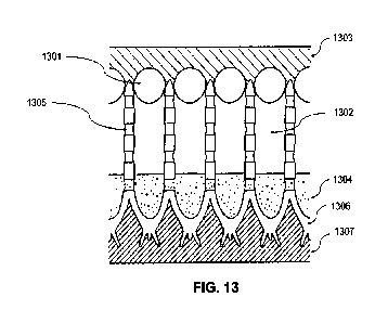
a band of black or grey color as shown by bar 803 in FIG. 8. However, higher
anodizing voltages may form wider pores with a corresponding ease of metal
deposition, which results in a compact metal layer at the base of the pores.
Here, the coating color is dominated by a combination of light absorption
within the pores, as previously described, and a blue spectrum of colors that
are developed by selective absorption of light traversing the barrier layer
(e.g., the barrier layer 902 illustrated in FIG.9) of these thicknesses. As
the
anodizing voltage increases, the pores widen, and a predominant color is
developed for each anodizing voltage, from violet purple (the bar 803 of FIG
8), shades of blue (bars 804-806 of FIG. 8.), greens (bars 807-808 of FIG.
8.),
yellow (bar 809 of FIG.8.), oranges (bar 811-812 of FIG. 8.), and red (bar 813
of FIG. 8.). As the pores widen, the range of metal deposition amp-minutes
during which color is perceivable increases.
[0om] As metal deposition amp-minutes increases, the average pore
filling also increases. At high amp-minutes, metallic colors predominate (as
shown by bars 801 in FIG. 8). However, due to variations in the nucleation
process, a periodic range of filling occurs (e.g., as illustrated in the image
shown in FIG. 5). Three color generation mechanisms compete to develop the
perceived coating color. Firstly, the depth of the deposited metal controls
the
amount of light absorption. Here, the filling of the side pores presents extra
absorbance by plasmonic effects, as shown by the image in FIG. 5.
[00112] Secondly, light that is refracted and reflected down
between the
barrier layer and underlying aluminum substrate is then filtered in a manner
decided by the geometry and length of the light pipe (e.g., the light path
illustrated by the line 940 in FIG. 9). The frequency selectivity of this
light
27
CA 03175978 2022- 10- 17
WO 2021/215939
PCT/NZ2021/050067
pipe is proportional to its length, which depends on the depth of the metal in
the pores, the pore diameter, and anodized film barrier layer thickness.
Those skilled in the art will recognize that there are multiple effective
lengths of the light pipe depending on the incident angle and associated
reflections; thus, there is a spectrum of transmission and absorption.
[00113] Lastly, light is directly reflected from the metal
surface, where the
distance between the metal surface, and top of the pore produces either
destructive or constructive interference depending on the path length and
light
wavelength, as illustrated by the light path shown by lines 920 ad 922 in FIG.
9.
[00114] The distribution of wavelengths that exit the coating produces the
perceived color of the coating, and the total absorption of incident light
within
the structure gives rise to the darkness or decreased luminance of the
resultant
color, where at the extreme, the coating tends towards black. Narrower pores,
and consequently narrower side walls, are more constrained light paths, which
give rise to greater control over the coating color. This may lead to wider
bands
of metal deposition over which a single color is perceived.
[00115] Table 1 shows the color produced (RGB) and color
variation across
the surface (AE) for several anodizing voltages and temperatures, higher
temperatures in any bath formulation increases the porosity of the anodizing
and darkens the color.
Table 1:
Anodizing Color
V C Name R G BAE
60 24.0 Light Grey 130 132 139 1.9
60 25.5 Dark Grey 73 75 81 1.3
60 27.0 Black 37 44 52 1.1
70 27.0 Dark Blue/Purple 67 88 143
1.3
80 27.0 Dark Blue 44 72 125 1.6
80 28.0 Mid Blue 43 107 187 0.5
90 27.0 Blue 44 76 144 1.5
28
CA 03175978 2022- 10- 17
WO 2021/215939
PCT/NZ2021/050067
100 28.0 Light Blue 71 114 145
1.3
110 30.0 Blue Green 77 127 152
1.3
120 27.0 Baby Blue 112 163 202
.. 0.7
130 23.0 Blue Grey 150 168 179
0.6
160 36.0 Bronze 129 107 86 2.0
EXAMPLE 4 ¨Relationship between Phosphoric Acid Concentration
and Maximum Anodizing Thickness
[00116] Fifteen substrates of 6061-T6 aluminum were prepared identically.
[00117] Each sample was then soaked for 10 minutes in a
commercial
alkaline Prelude AC-100 bath at 70 C with light air agitation to remove
surface contamination. The samples were dipped in 50% nitric acid to de-
smut the surface. The samples were rinsed in DI water between each step.
[00118] The anodizing bath composition was H3PO4 (between 100 m1/I and
210 m1/I depending on the sample), H2SO4 (0.6mL/L), and HOOCCOOH (1g/L)
in each case. The counter electrode was titanium mesh, and vigorous air
agitation was used to refresh the anodizing bath electrolyte at the example
surfaces. The anodizing bath was placed in a water bath, and the temperature
of the solution was maintained at 25 1 C.
[00119] Constant voltage DC anodizing was employed, with voltage
limited to
60 V. In addition, the maximum current was limited to 2.0 A/dm2. Anodizing
was performed for a variety of periods of between approximately 20 minutes
and 120 minutes. The period was determined by the total charge passed,
which was calculated for each sample processing from the record of measure
voltage and current over the anodizing period.
[00120] Each sample was rinsed in DI water and thoroughly dried.
The samples
were cross sectioned and mounted as metallographic specimens, and the
anodizing film thickness was measured.
[00121] FIG. 11 illustrates an example graph showing the maximum
29
CA 03175978 2022- 10- 17
WO 2021/215939
PCT/NZ2021/050067
achievable anodizing layer thickness for several phosphoric acid
concentrations of the present disclosure. The graph 11 01 shows the
relationship between the maximum anodizing film thickness achievable for
the phosphoric acid concentration in the bath. As mentioned previously, thick
films provide improved mechanical properties of the coating at the expense
of time to generate the film and clarity of the colored coating.
EXAMPLE 5¨ The Effect of Barrier Layer Thinning and Anodizing
Bath Temperature on a Dark Grey Colored Coating
[00122] Five substrates of 6022-T4 aluminum were prepared
identically.
[00123] Each sample was then soaked in for 10 minutes in a
commercial
alkaline Prelude AC-100 bath at 70 C with light air agitation to remove
surface contamination. The samples were soaked in a Probright AITM alkaline
cleaner at room temperature for 2 minutes. The samples were then de-
smutted in 50% nitric acid at room temperature for 90 seconds. The samples
were electropolished in a bath containing H3PO4, HF, H2SO4, and glycerol
in a volume ratio selected from the following ranges 70-85:2-4:6-9:5-20. The
electropolishing bath was held at a temperature of 65 Celsius ( C) at a
voltage
(V) of 12V and a Pb counter electrode for a period between 0 and 8 minutes.
The samples were rinsed in DI water between each step.
[00124] The anodizing bath composition was H3PO4 (between 150
m1/I and
250 m1/1, depending on the sample), H2SO4 (0.6mL/L), and HOOCCOOH
(1g/L) in each case. The counter electrode was titanium mesh, and vigorous
air agitation was used to refresh the anodizing bath electrolyte at the
example
surfaces. The anodizing bath was placed in a water bath, and the temperature
of the anodizing bath was maintained using ice, such that the temperature
varied between 27 and 33 3 C depending on the sample.
[00125] Constant voltage DC anodizing was employed, with voltage limited
CA 03175978 2022- 10- 17
WO 2021/215939
PCT/NZ2021/050067
to 60 V. In addition, the maximum current was limited to 2.0 A/dm2.
Anodizing was performed for 20 minutes, and a variety of barrier layer
thinning periods were applied to each sample, for a total of 10 to 12 minutes
of reduced anodizing voltage(s) of 30 V and/or 15 V. After anodizing, the
samples were rinsed in DI water and immediately placed in the electroplating
bath.
[00126] The samples were placed in a Chemipure/Niflow semi-bright
nickel-
plating bath, commercially available from CMP India. The bath was
maintained at 60 C, and the anode was nickel chips in a bagged titanium
mesh basket. The samples were initially soaked for 3 minutes to allow the
nickel ions to penetrate the pores. The plating current was ramped from 0 to
0.1A/dm2over a period of 2 minutes, after which the current was maintained
at 0.1 A/dm2 for a further 2 minutes, after which the current was increased to
0.3A/dm2 for a further period of 10 minutes. The samples were then rinsed
and dried.
[00127] FIG. 12 is a set of example images and a table showing
the
effects of barrier layer thinning and temperature on the coating color
of the present disclosure. FIG. 12 shows resulting samples 1201-
1205, color profiles, and anodizing temperatures. The anodizing bath
temperature slightly affects pore size and barrier layer thickness, but
significantly affects the total dissolution rate of the anodized layer in
the phosphoric acid bath. The level and extent of barrier layer
thinning also controls how much of the visible spectrum of light is
filtered out from the light that is reflected out of the coating. This gives
rise to the variation in color, where in FIG. 12 the five samples 1201 ¨
1205 all exhibit a dark grey color, but samples 1201, 1202, and 1205
include a blue hue; sample 1203 includes a red hue; and sample 1204
displays a hue of orange-yellow. Table 1206 provides various
processing parameters for each one of the samples 1201-1205.
EXAMPLE 6 ¨ Effect of Copper on Color
31
CA 03175978 2022- 10- 17
WO 2021/215939
PCT/NZ2021/050067
[00128] Three substrates of 6061-T6 aluminum, and three
substrates of 6022-
T4 aluminum were prepared identically.
[00129] Each sample was soaked for 10 minutes in a commercial
alkaline Prelude AC-100 bath at 70 C with light air agitation to remove
surface contamination. The samples were dipped in 50% nitric acid to de-
smut the surface. The samples were rinsed in DI water between each
step.
[00130] The anodizing bath composition was H3PO4 (between 30 m1/I
and 300
m1/I depending on the sample), H2SO4 (0.6mL/L), and HOOCCOOH (1g/L) in
each case. The counter electrode was titanium mesh, and vigorous air agitation
was used to refresh the anodizing bath electrolyte at the example surfaces.
The
anodizing bath was placed in a water bath, and the temperature of the solution
was maintained at 25 1 C.
[00131] Constant voltage DC anodizing was employed with voltage limited
in the range of 60 - 100 V depending on the 6061/6022 comparison pair of
samples. In addition, the maximum current was limited to 2.0 A/dm2.
Anodizing was performed for a variety of periods of between approximately
minutes and 120 minutes. The period was determined by the total charge
20 passed, which was calculated for each sample processing from the record
of
measured voltage and current over the anodizing period.
[00132] Each sample was rinsed in DI water and thoroughly dried.
The samples were cross sectioned and mounted in resin via
metallographic preparation. The anodizing film was inspected for pore
size as well as the prevalence, size, and frequency of side pores (1204
in FIG. 12) creating interporosity.
[00133] As shown in Table 1 below, for an identical anodizing
voltage and
charge passed, the 6061 samples had larger and more numerous side pores
compared to 6022 samples; however, the 6022 aluminum alloy samples had
wider pore diameters. The side pore volume developed is roughly
32
CA 03175978 2022- 10- 17
WO 2021/215939
PCT/NZ2021/050067
proportional to the copper content of the alloy, while the main pore volume
change is related to the side pore volume.
[00134] The luminance measured for the 6022 and 6061 aluminum
alloy
samples was 45.4 and 25.8, respectively. The change in luminance directly
corresponds to the side pore diameter variation, the postulated light
absorption by side pores 923, and the light path represented by the line 920
illustrated in FIG. 12, and described above.
Table 2:
Alloy Cu wt.% d-pore d-side Main Pore Side-pore Total
Pore
base (rim) pore (nm) Volume ( /0) volume ( /0) volume (%)
6022 0.01-0.1 98.8 6.1 24.1 1.7 37.7 10.0
2.9 0.8 40.6 10.8
6061 0.15-0.4 85.0 6.9 50.4 5.5 24.9 4.0
18.2 5.0 43.1 9.0
EXAMPLE 7¨ The Effect of Pore Plugging and Sealing
[00135] Ten 100 x 25 mm 6061 aluminum substrates were anodized and
colored to produce a dark grey surface as previously described. Samples were
either unsealed, sealed with DUDMA only, or pMMA nano pore plugged (to
retain the air gap) followed by a DUDMA seal.
[001 36] For the DUDMA seal, a solution of ZnO nanoparticles in DI water
was
applied to the surface and dried to act as a surface initiator and retain the
clarity of the pDUDMA coating. The surface was then dipped three times in
pure DUDMA monomer diluted 80% by volume with Tetrahydrofuran (THE)
and an organic to control the evaporation, e.g. acetone or ethyl acetate.
Samples were exposed to intense UV light, with a principal wavelength 365nm,
while being simultaneously heated to 75 5 C. After 30 minutes the DUDMA
polymerized to a transparent coating.
[001 37] MMA nanoparticles were previously prepared to plug the openings of
the porous anodized coating. 180 mL of deionized water, with 0.070 g
33
CA 03175978 2022- 10- 17
WO 2021/215939
PCT/NZ2021/050067
Potassium Bicarbonate (KHCO3), 0.024g Ammonium Persulfate (APS), and
0.029 g Sodium Dodecyl Sulfate (SOS), was added to a 300mL Erlenmeyer
flask, stirring at 600 rpm by magnetic stirring The solution was heated to 75
00, where 5 mL of Methyl Methacrylate (MMA) monomer was added to the
flask, followed by 0.0070 g of Sodium Bisulfite (NaHS03). The flask was
loosely sealed with a stopper, and the temperature monitored over the 3 hours.
The solution was then removed immersed into an ice bath to rapidly cool to
room temperature.
[00138] Thermogravimetric analysis showed a yield of 90%
conversion of MMA
monomer to PMMA nanoparticles. Dynamic Light Scattering showed the
average particle size to be 110 nm, with a polydispersity index of 0.02.
[00139] Color change was measured by photographing that samples
in a light
cabinet with the images processed in Imagej software to determine the color in
RGB and variance between the average color between the sample AE as.
LE = AI (0- 02 (0- )2 (0B)2
[00140] The sealed sample provided 8-times improvement in
corrosion
performance as shown in Table 2 but the apparent color was perceptibly
different. This different was more noticeable with lighter samples where the
AE
was > 20. The samples with the nanoparticle pore plug and pDUDMA seal had
a 20-times improvement is corrosion resistance and an imperceptible color
change.
[00141] Corrosion performance was measured by neutral salt spray
testing
following standard B117. Samples rinsed dried and analyzed daily for
corrosion. The time to first corrosion was recorded.
Table 3:
Seal Description Hours until first corrosion Sample color
change AE
point
Unsealed control 48 n/a
pDUDMA seal 336 5.1
34
CA 03175978 2022- 10- 17
WO 2021/215939
PCT/NZ2021/050067
pMMA NP Plug and 1100 0.1
pDUDMA Seal
[00142] It will be appreciated that variants of the above-
disclosed and other
features and functions, or alternatives thereof, may be combined into many
other different systems or applications. Various presently unforeseen or
unanticipated alternatives, modifications, variations, or improvements
therein may be subsequently made by those skilled in the art which are also
intended to be encompassed by the following claims.
35
CA 03175978 2022- 10- 17