Note: Descriptions are shown in the official language in which they were submitted.
CA 03179533 2022-10-05
WO 2021/206735 PCT/US2020/027781
ONBOARD FIELD WEAKENED AC CHARGER
FIELD OF THE DISCLOSURE
[0001] This disclosure relates to chargers for an energy storage system from a
three-phase AC
power source. More particularly, this disclosure relates to charging an energy
storage system in a
vehicle from an external three-phase AC power source.
BACKGROUND
[0002] Hybrid electric vehicles and electric vehicles have energy storage
systems. These
systems may be charged using power from an external power source. For example,
the energy
storage system may be charged using power from a three-phase AC power grid.
However, there
can be a problem where a passively rectified grid voltage overlaps with the
energy storage
system voltage range (VL-LRMS * sqrt(2) > Vbattery min). There are many
different types of
chargers including chargers that employee a boost rectification. Ideally for
boost rectifier
operation when in a non-isolated configuration, the rectified grid voltage is
less than the battery
voltage in all states. When the passively rectified grid voltage is higher
than the current voltage
of the energy storage device, the conversion circuitry may operate like a
diode (passive) rectifier
and could damage the energy storage system or overcharge the same.
[0003] One known charging system solves this by using an isolated converter.
However, isolated
converters are typically less efficient than non-isolated converters. Isolated
converters are also
typically more costly and complex.
SUMMARY
[0004] Accordingly, disclosed is a charging system for a vehicle. The vehicle
may be a hybrid
electric vehicle. In other aspects, the vehicle may be an electric vehicle.
When in use, the
charging system is coupled to an external three-phase AC power source and used
to charge an
energy storage system in the vehicle.
[0005] The charging system may comprise one or more switches for the AC power
source, an
AC filter, conversion circuitry, voltage sensors, one or more switches for the
energy storage
system, and a processor.
1
CA 03179533 2022-10-05
WO 2021/206735 PCT/US2020/027781
[0006] The AC filters may comprise an inductor. Each AC filter may be coupled
to the three-
phases of the AC power source, respectively.
[0007] The conversion circuitry may be coupled to the inductor of each AC
filter. The
conversion circuitry may be configured to convert three-phase AC power
received at its input
terminals into DC power for a system DC bus and may be configured to supply an
independently
controllable real AC current and reactive AC current. The voltage sensors may
detect a voltage at
each of the three-phases at the input terminals of the conversion circuitry.
[0008] The energy storage system may be connected to or isolated from the
system DC bus via
the one or more switches under the control of the processor. The one or more
switches may be
external to the energy storage system. In other aspects, the one or more
switches may be
incorporated into the energy storage system.
[0009] The processor may be configured to close the one or more switches
associated with each
of the three-phases when a condition is satisfied, determine a peak line-line
voltage
corresponding to the detected voltage at the input terminals of the conversion
circuitry; and
compare the determined peak line-line voltage with a real time voltage of the
energy storage
system to be charged.
[0010] When the determined peak line-line voltage is larger than or equal to
the real time voltage
of the energy storage system, the processor may be configured to calculate the
reactive AC
current to reduce the peak line-line voltage at the input terminals of the
conversion circuitry to
less than the real time voltage of the energy storage system, and cause the
reactive AC current to
be supplied by the conversion circuitry such that it flows through each
inductor. This reduces the
peak line-line voltage at the input terminals of the conversion circuitry.
[0011] The processor may also be configured to regulate the system DC bus to
substantially
match the real time voltage of the energy storage system and control the one
or more switches
associated with the energy storage system to close once the peak line-line
voltage is less than the
real time voltage of the energy storage system and the system DC bus voltage
substantially
matches the real time voltage of the energy storage system.
[0012] The processor may also be configured to control the charging of the
energy storage
system. In some aspects, the processor may be configured to control the real
AC current to
charge the energy storage system. In other aspects, the processor may be
configured to regulate
the system DC bus voltage to charge the energy storage system.
2
CA 03179533 2022-10-05
WO 2021/206735 PCT/US2020/027781
[0013] The reactive current may be calculated via an opened or closed control
loop and may be
continuously adjusted.
[0014] In some aspects, the reactive AC current is calculated based on the
following equation:
¨Vac (Vess¨Vm)2
Id = ¨+ Iq2,
weLs N 3Ls2coe2
where Vac is a peak-line neutral voltage of the three-phase power source, we
is the frequency of
the three-phase power source, Ls is the inductance of inductor, Vess is the
real time voltage of
the energy storage system and Vm is the voltage margin, Id is the reactive AC
current and Iq is
the real AC current.
[0015] In some aspects, the reactive current may be calculated such that the
peak line-line
voltage is a predetermined value less than the real time voltage of the energy
storage system.
[0016] When entering a charge mode (e.g., in response to a receipt of a
signal), the processor
may be configured to open the one or more switches associated with the energy
storage system
when receiving the signal from another controller or the energy storage system
to charge the
energy storage system to isolate the energy storage system from the system DC
bus.
[0017] In some aspects, the processor may be configured to control at least
one of the real AC
current and real voltage Vq to regulate the system DC bus to substantially
match the voltage of
the energy storage system prior to closing the one or more switches associated
with the energy
storage system.
[0018] In some aspects, the processor is configured to cause reactive AC
current by injecting the
reactive AC current through each inductor of each AC filter causing field
weakening.
BRIEF DESCRIPTION OF THE DRAWINGS
[0019] Fig.1 is a diagram of a charging system in accordance with aspects of
the disclosure for
charging an energy storage system and the energy storage system;
[0020] Fig. 2 is a flow diagram for charging an energy storage system using
field weakening in
accordance with aspects of the disclosure;
[0021] Fig. 3 is a flow diagram for charging an energy storage system using
field weakening in
accordance with other aspects of the disclosure;
3
CA 03179533 2022-10-05
WO 2021/206735 PCT/US2020/027781
[0022] Fig. 4 is a diagram of the converter stage of Fig. 1 in accordance with
aspects of the
disclosure;
[0023] Fig. 5 is a diagram of a PI controller used for determining a reactive
current for field
weakening in accordance with aspects of the disclosure;
[0024] Fig. 6 is a diagram shown an example of the control for field
weakening, system DC bus
voltage regulation and charging the energy storage system in accordance with
aspects of the
disclosure; and
[0025] Fig. 7 is a diagram shown an example of the control for field
weakening, system DC bus
voltage regulation and charging the energy storage system in accordance with
other aspects of
the disclosure.
DETAILED DESCRIPTION
[0026] For purpose of this description, the control is a variant of the
classic permanent magnet
machine vector control. The basic equations are:
Vq = Vac + IqRs + IdweLs (1)
Vd = IdRs ¨ IqweLs (2)
P = -3 (VdId + VqIq) (3)
2
All variables are peak line-neutral. Id is defined as the reactive current
into the grid and Iq is
defined as the real current. Vac is the peak line-neutral voltage at the grid,
which is in phase
with the q axis. Vd and Vq are in phase with Id and Iq respectively, and
represent peak line ¨
neutral voltages at the power converter terminals. Rs is the resistive
component of the filter and
grid impedance and Ls the reactive component. we is the grid frequency in
radians/second. P is
the power transferred to the Energy storage system; negative Iq is required to
transfer power
from the grid to the energy storage system.
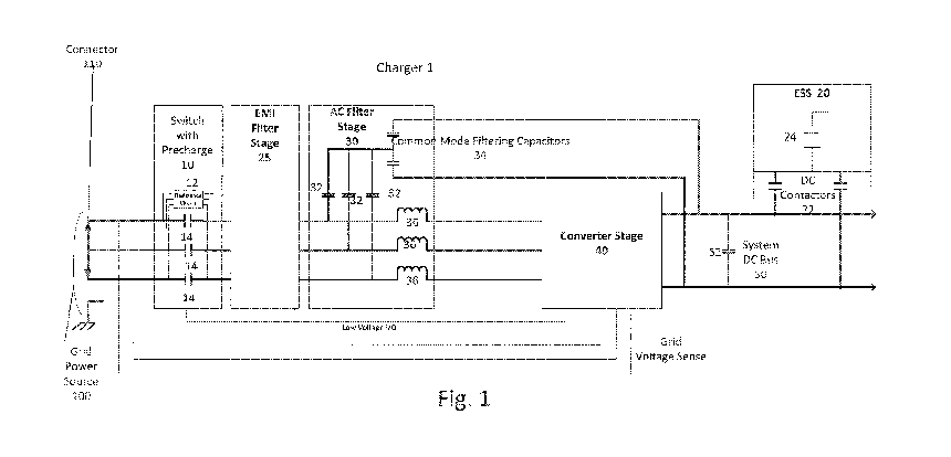
[0027] Fig. 1 shows a schematic diagram of a charging system (also referred to
herein as charger
1) for charging an energy storage system (ESS) 20 using an external power
source, e.g., grid
power source 100. In an aspect of the disclosure, the charger 1 is installed
in a vehicle
(onboard), such as an electric vehicle or a hybrid electric vehicle. The term
vehicle used herein
means a car, bus, taxi, vessel, airplane, UAV, UUV, train, tank, truck, or
helicopter. The hybrid
electric vehicle may be in a series hybrid configuration or a parallel hybrid
configuration. In an
4
CA 03179533 2022-10-05
WO 2021/206735 PCT/US2020/027781
aspect of the disclosure, the ESS 20 may be a high voltage energy storage.
High used herein
means a voltage above 50V. The ESS 20 may be used for power for propulsion.
[0028] In other aspects of the disclosure, the ESS 20 may be an accessory
battery and used for
powering AC and DC accessories.
[0029] In an aspect of the disclosure, the charger 1 is configured as a single
stage non-isolated
converter. This saves the design time of creating an isolated converter and is
more efficient
because of the single stage of the power conversion.
[0030] Fig. 1 does not show components of the vehicle other than the charger 1
and ESS 20.
However, certain other components of the vehicle may also be coupled to the
charger 1 and/or
ESS 20. For example, in a case of a hybrid electric vehicle, the vehicle would
have a prime
mover, such as an engine or fuel cell. The engine may use gasoline, or the
engine may be a diesel
engine or a compressed natural gas (CNG) engine. A generator would be
mechanically
connected or coupled to the engine, such as via a shaft, belt/pulley system,
gearbox, etc.
[0031] When coupled to the engine (referred to herein as the genset), the
generator provides
three-phase AC electrical power and may be a high voltage generator. The
generator may also be
electrically coupled to a converter stage 40 (such as the converter stage
shown in Fig. 1). Thus,
the generator, via the converter stage 40, also supplies power to the System
DC bus 50 (DC
Link) and ESS 20. In other aspects of the disclosure, a separate converter
stage may be used for
the generator (other than the converter stage in the charger 1).
[0032] The System DC bus 50 may be connected to another converter stage for
converting the
system DC bus 50 to AC for an AC traction motor. The System DC bus 50 supplies
power to the
AC traction motor via the another converter stage. The traction motor in turn
may be
mechanically connected to a transmission system, axle(s) and wheels. The type
of components
in the vehicle (such as for propulsion) may depend on the type of vehicle. For
example, an
airplane and train would have different components than a bus.
[0033] The vehicle may also have one or more control systems. One of the
control systems may
be used for controlling the propulsion of the vehicle. For example, there is a
control system
which receives operator commands via the user interfaces, e.g., gas pedal and
brake, and
generates torque and/or power commands for the converters and generator
(coupled to the engine
in a case the vehicle is a hybrid electric vehicle).
CA 03179533 2022-10-05
WO 2021/206735 PCT/US2020/027781
[0034] This control system may also be in communication with the ESS 20 via a
control area
network (CAN).
[0035] The grid power source 100 may be a utility grid. In an aspect of the
disclosure, the grid
power source 100 provides three-phase. For example, the grid power source 100
may provide
400V at 50Hz. The value and frequency of the source is provided, only by way
of example, and
other voltages and frequencies may be used. The grid power source 100 may be a
dedicated
vehicle charging station. In other aspects of the disclosure, the power source
100 may be an
external generator, building local high voltage junction box, or shore power.
[0036] In an aspect of the disclosure, the charger 1 may be coupled to the
grid power source 100
using a connector 110. The connector 110 may be a connection system with High
Voltage
Interlock Loop (HVIL). The connector 110 may also have Electromagnetic
Interface Shielding
(EMI) for noise reduction. The connector 110 includes a ground wire.
[0037] The charger 1 may comprise a switch with precharge (shown schematically
in Fig. 1 and
identified as "10"). Each phase line has a AC switch. In some aspects, the AC
switch(es) 14 may
be a relay (an electrically operated switch). For high power applications, the
relay may be a
contactor. In other aspects of the disclosure, the switches may be
semiconductor based, such as a
MOSFET. In other aspects of the disclosure, a mechanically operated switch may
be used.
[0038] When the AC switch(es) 14 is closed, the grid power source 100 is
electrically coupled
with the converter stage input terminals (shown in Fig. 4 as terminal(s) 402).
When the AC
switch(es) 14 is open, the grid power source 100 is electrically isolated by
the input terminals
402. In Fig. 1, three switch(es) 14 are shown (one for each line), however, in
other aspects of the
disclosure, a single switch may be used for all three-phases. In an aspect of
the disclosure, a
processor in the converter stage 40 (shown in Fig. 4 identified as "410")
controls the switch(es)
14 (as shown in Fig. 1 by Low Voltage I/0).
[0039] The charger 1 may have inrush current protection (precharge). As shown
in Fig. 1,
resistance circuit 12 is placed in parallel with the switch(es) 14. In some
aspects of the
disclosure, the resistance circuit 12 comprises a resistor in series with a
switch. The resistor may
have a fixed value. A processor in the converter stage 40 may control the
switch to close upon
detection of the grid power source 100 (connection). Once the precharge
current has effectively
zeroed through the system, the processor 410 may open the switch (in series
with the resistor). In
6
CA 03179533 2022-10-05
WO 2021/206735 PCT/US2020/027781
other aspects, the resistance maybe provided by an NTC thermistor. The NTC
thermistor may
also be placed in series with the switch.
[0040] The charger 1 may also comprise an EMI Filter Stage 25 and an AC Filter
Stage 30. The
EMI Filter Stage 25 is also for reducing noise. The circuitry used for an EMI
Filter Stage 25 is
well known and a commercial off the shelf EMI filter may be used.
[0041] The AC Filter Stage 30 may comprise a LC circuit for each phase
(capacitor 32 and
inductor 36). As shown in Fig. 1, the AC Filter Stage 30 is configured in a
common mode. The
stage 30 also comprises common mode filtering capacitors 34. However, other
configurations for
the AC filter stage 30 are possible and the configuration of the stage 30 is
not limited to the
depicted configuration.
[0042] The charger 1 may also comprise a converter stage 40. A schematic
diagram of the
converter stage 40 is shown in Fig. 4.
[0043] As shown in Fig. 4, the converter stage 40 may comprise three input
terminals 402, one
input terminal for each phase. The converter stage 40 may comprise a voltage
sensor 400 for
each phase and a voltage sensor 400 for the DC link. The converter stage 40
may also have
current sensors 405. In some aspects, there may be a current sensor for each
phase as well. In
other aspects of the disclosure, only two current sensors may be used for the
AC link. As
depicted, the voltage sensors 400 and current sensors 405 are located within
the converter stage
40, however, in other aspects of the disclosure, the sensors 400/405 may be
external to the
converter stage 40. As depicted, there is a current sensor 405 for the ¨DC.
However, in other
aspects, the current sensor 405 may be on the +DC. Further, in other aspects,
both the +DC and ¨
DC may have current sensors 405.
[0044] In an aspect of the disclosure, the current sensors 405 may be hall
effect sensors. In other
aspects of the disclosure, a current sensing shunt resistor circuit may be
used.
[0045] The converter stage 40 may also comprises a processor 410. The
processor 410 is
coupled to the voltage sensors 400 and current sensors 405. The processor 410
may be an FPGA.
In other aspects of the disclosure, the processor 410 may be a microcontroller
or microprocessor
or any other processing hardware such as a CPU or GPU. Memory may be separate
from the
processor (as or integrated in the same). For example, the microcontroller or
microprocessor
includes at least one data storage device, such as, but not limited to, RAM,
ROM and persistent
storage. In an aspect of the disclosure, the processor may be configured to
execute one or more
7
CA 03179533 2022-10-05
WO 2021/206735 PCT/US2020/027781
programs stored in a computer readable storage device. The computer readable
storage device
can be RAM, persistent storage or removable storage. A storage device is any
piece of hardware
that is capable of storing information, such as, for example without
limitation, data, programs,
instructions, program code, and/or other suitable information, either on a
temporary basis and/or
a permanent basis.
[0046] The processor 410 receives the sensed voltage(s) and current(s) from
the sensors and
calculates certain values in accordance with aspects of the disclosure based
thereon such as, but
not limited to, a peak line-line voltage.
[0047] The converter stage 40 may also comprise conversion electronics 425 for
converting AC
into DC and vice versa under the control of the processor 410 and injecting a
reactive current.
The conversion electronics 425 may comprise switches such as MOSFETS for each
phase. The
processor 410 may function as a gate driver for the switches.
[0048] The converter stage 40 may also comprise output terminals 404 for the
System DC bus
50 (one positive and one negative). In some aspects of the disclosure, the
converter stage 40 may
also comprise voltage sensors for detecting a grid voltage including phase
(sensors not shown in
Fig. 4). The voltage sensor may also be external to the converter stage 40.
[0049] The converter stage 40 may also comprise a communication interface 415.
This interface
415 may be a CAN interface for communicating with other control systems in the
vehicle such as
the control system for propulsion control and for communicating with the ESS
20.
[0050] The ESS 20 provides a direct current (DC) electrical power to the
System DC bus 50.
The ESS 20 may include lithium ion batteries (shown as "24" in Fig. 1). In an
aspect of the
disclosure, the nominal voltage of the System DC bus 50 may be above 600V. A
capacitance 52
is connected between the lines of the System DC bus 50.
[0051] The ESS 20 may also alternatively include ultra-capacitors, lead-acid
batteries, and other
energy storage mediums. The ultra-capacitor may include an electric double-
layer capacitor
(EDLC), also known as a supercapacitor, a supercondenser, or an
electrochemical double layer
capacitor, which has an electrochemical capacitor with relatively high energy
density.
[0052] The ESS 20 may also comprise a switch(es) (e.g., DC contactors 22) for
selectively
electrically connecting/isolating the ESS 20 from/to the System DC Bus 50. In
some aspects of
the disclosure, the DC contactors 22 are controlled by the processor 410.
8
CA 03179533 2022-10-05
WO 2021/206735 PCT/US2020/027781
[0053] Fig. 2 illustrates a method of charging an ESS 20 in accordance with
aspects of the
disclosure. At S200, a charge command is received by the processor 410. In an
aspect of the
disclosure, the charge command may be received from the ESS 20. In this aspect
of the
disclosure, the ESS 20 may indicate to the processor 410 that the cells need
to be charged. In
another aspect of the disclosure, a control system, such as the system for
controlling propulsion
may issue a command or instruction to the processor 410 to charge the ESS 20.
In other aspects
of the disclosure, instead of receiving a command from another control system
or the ESS 20, the
processor 410 may detect a connection with the grid power source 100 and
initiate a charging
session. In accordance with this aspect, the grid voltage may be sensed by
voltage sensors. In
other aspects of the disclosure, the processor 410 may directly sense the
voltage of the ESS 20.
When the sensed voltage is below a preset threshold, the processor 410 may
initiate the charging
session. When a charging session is initiated, the processor 410 controls the
DC contactors to
open 22 (if closed) to isolate the ESS 20 from the system DC bus 50. This may
be done using a
low voltage control signal.
[0054] At S205, precharging occurs followed by the closing of the AC
switch(es) 14 (and
opening the switch in the resistance circuit 12). When a resistor is used for
the precharging
(inrush protection), the processor 410 closes the AC switch(es) 14 when a
predetermined time
has elapsed or once the precharge current has effectively zeroed in the
system. The processor 410
issues a control signal to the switch(es) 14. In an aspect of the disclosure,
the control signal is a
low voltage control signal which actuates the switch(es) 14 (shown in Fig. 1
as "Low Voltage
I/0"). In other aspects of the disclosure, where a resistor in series with a
switch is used as the
precharging, the processor 410 will also control the switch (in series with
the resistor) to close
when the charge command is received and open after a predetermined time or
current flow.
Subsequently, the processor 410 will control the switch(es) 14 as described
above.
[0055] At this point in time, the ESS 20 is electrically isolated from the
System DC Bus 50, e.g.,
DC contactors 22 are open.
[0056] At S210, the voltages at each input terminal are sensed via the voltage
sensors 420, e.g.,
localized voltage. Also, the voltage of the ESS 20 is determined. In an aspect
of the disclosure,
the processor 410 may directly measure the voltage of the ESS 20 via a sensor.
In other aspects
of the disclosure, the processor 410 receives a real time voltage of the ESS
20 from the ESS 20
via CAN.
9
CA 03179533 2022-10-05
WO 2021/206735 PCT/US2020/027781
[0057] Using the real time voltage of the ESS 20 and the sensed voltages at
the terminals 402,
the processor 410 determines whether field weakening is needed at S215. The
processor 410 may
convert the voltages detected at each terminal into a dq space, e.g., Vd and
Vq voltage. Once
converted, the processor 410 determines the total localized voltage Vs at the
converter terminals
using the following equation:
Vs = \1Vq2 +Vd2 (4)
[0058] Based on total Vs, the processor then determines the peak line-line
voltage VLL. In other
aspects of the disclosure, instead of converting the sensed phase voltage into
Vd and Vq, the
processor 410 may calculate the VLL directly from the phase voltage.
[0059] The processor 410 compares the peak line-line voltage VLL with the real
time ESS
voltage. When the peak-line-line voltage VLL is greater than or equal to the
real time voltage of
the ESS, the processor 410 may determine that field weakening is needed ("Y"
at S215). On the
other hand, when the peak line-line voltage VLL is less than the real time
voltage of the ESS,
field weakening is not needed and S220 and S225 are skipped ("N" at S215).
[0060] In other aspects of the disclosure, a voltage margin VM may also be
used. The voltage
margin may account for deadtime, controls, switching drop, etc. In this case,
when the peak line-
line voltage VLL is greater than the real time voltage of the ESS minus VM,
the processor 410
determines that field weakened is needed.
[0061] At S220, the processor 410 determines the amount of field weakening.
Field weakening
is achieved by injecting a reactive current Id such that it flows through each
inductor 36. This
reduces the peak line-line voltage at the input terminals 402. In an aspect of
the disclosure, the
reactive current Id is determined by the following equation:
¨Vac , (V ess)2
Id = ¨+ Iq2 (5)
weLs N 3Ls2 coe2
where Vac is the peak-line neutral voltage of the grid power source 100, we is
the frequency of
the voltage of the grid power source 100, Ls is the inductance of inductor 36,
and Vess is the real
time voltage of the ESS. When a voltage margin is used, Id is calculated with
the following
equation:
¨Vac , (V ess¨Vm)2
Id = ¨+ Iq2 (6)
weLs N 3Ls2 coe2
CA 03179533 2022-10-05
WO 2021/206735 PCT/US2020/027781
where Vac is the peak-line neutral voltage of the grid power source 100, we is
the frequency of
the voltage of the grid power source 100, Ls is the inductance of inductor 36,
Vess is the real
time voltage of the ESS and Vm is the voltage margin.
[0062] When Id is less than zero, field weakening will occur. The more
negative Id is, the
stronger the field weakening will be.
[0063] In other aspects of the disclosure, the reactive current Id, will be
determined via a PI
controller (shown in Fig. 5).
[0064] At S225, once the reactive current Id is determined, the processor 410
will cause the
same to be injected to flow through the inductors 36. For example, the
processor 410 will control
the conversion electronics 425 to provide the determined reactive current Id.
For example, the
processor 410 may control the gates of the respective switches such that the
switches open and
close as appropriate.
[0065] One example of the control is shown in Fig. 6. As shown in Fig. 6, the
processor 410 may
execute a plurality of PI controls (including PI controller 610).
[0066] The processor 410 uses the current Ix and Ty, sensed by the current
sensors 405, and
converts the same into Iq and Id (Id feedback and Iq feedback, respectively)
via coordinate
transformation 670. The transformation has two portions Ixy to Ic43 and then
Ic43 to Idq.
[0067] The phase 0 and voltage of the grid power source 100 determined by a
phase lock loop
PLL 665. In one aspect of the disclosure, voltage sensors 400 in the converter
stage 40, may
detect the voltage and phase 0. In other aspects of the disclosure, the
voltage may be detected by
an observer.
[0068] The PLL outputs the phase 0 to the transformation. The phase 0 is used
in the
transformation from Ic43 to Idq.
[0069] The calculated reactive current Id based on the above equation
(referenced in Fig. 6 as
"620") (or based on PI control) is supplied as a Id ref to adder 625, which
obtains the difference
between Id feedback and the determined reactive current Id. This difference is
an Id err (the
error signal). The PI controller 610 outputs a reference voltage Vd Ref which
causes the
measured value to reach the set point (determined reactive current Id). The
gains Kid and Kpd
are selected based on stability constraints and a desired convergence time. As
shown in Fig. 6,
feed forwards values are input into the PI controller 610. This is to decouple
a cross coupling
11
CA 03179533 2022-10-05
WO 2021/206735 PCT/US2020/027781
between the d-axis and the q-axis. The PI controllers also contain voltage
vector limiters which
prevent the peak line-line value of Vs from exceeding System DC bus 50.
[0070] The Vd command to the space vector modulation 690 is generated by
transforming the
output from the PI controller 610 (Vd Ref) from Vdq to Vc43. This
transformation also uses the
phase 0 of the grid power source 100.
[0071] The output of the space vector modulation controls the conversion
electronics 425.
[0072] Prior to closing the DC contactors 22 and charging the ESS 20, the
processor 410
regulates the System DC bus 50 to match the real time ESS voltage at S227.
[0073] An example of the voltage regulation is also shown in Fig. 6. The
regulation is performed
by a PI controller 600 (implemented by processor 410) in combination with
other PI controllers.
Here the set point is a Vdc command to match the real time voltage of the ESS
(set point is
shown as Vdc ref). A measured value (measured Vdc 650) is subtracted from Vdc
ref to generate
the error, e.g., Vdc err in adder 625. The PI controller 600 outputs a Iq Ref
which causes the
measured value to reach the set point. The gains KiV and KpV are selected
based on stability
constraints and a desired convergence time. At this time, the "mode" is set to
startup, meaning
that the charger 1 is not charging the ESS 20. As shown in Fig. 6, the mode
includes startup and
charge. Charge mode is where the ESS 20 is being charged by the charger 1.
[0074] In startup mode, Iq ref is set by the PI controller 600 (in charge
mode, Iq ref is set based
on the desired charge as described from equations 7or 8).
[0075] Additionally, Iq feedback is subtracted from Iq ref to generate the
error, e.g., Iq err in
adder 625. The PI controller 605 outputs a Vq Ref. The gains Kiq and Kpq are
selected based on
stability constraints and a desired convergence time. Similar feedforward
values and limiters are
input to the PI controller 605 (as PI controller 610) which serve the above
described functions.
[0076] The Vq command to the space vector modulation 690 is generated by
transforming the
output from the PI controller 605 (Vq Ref) from Vdq to Vc43. This
transformation also uses the
phase 0 of the grid power source 100.
[0077] The output of the space vector modulation controls the conversion
electronics 425 (e.g.,
switches).
[0078] Once the voltage of the system DC bus 50 is regulated to the real time
ESS voltage and
the reactive current Id is injected, the processor 410 closes the DC
contactors 22 (at S230). The
12
CA 03179533 2022-10-05
WO 2021/206735 PCT/US2020/027781
processor 410 may control the DC contactors 22 in a similar manner as
described above with a
low voltage control signal.
[0079] Subsequently, the ESS 20 is charged by the charger 1 at S235. Since as
a result of the
field weakening, the localized voltage (voltage at the terminals) is less than
the real time voltage
of the ESS, the converter stage 40 may act as a boost converter (boost
rectifier) and step up the
voltage. In particular, the field weakening is applied against the inductors
36 and there is a region
between the AC filter stage 30 and the converter having a localized voltage
reduction (as a result
of the field weakening.
[0080] In an aspect of the disclosure, the processor 410 via CAN receives a
request for a specific
power from the ESS 20. The processor 410 controls the conversion electronics
425 based on this
request. In an aspect of the disclosure, the processor 410 calculates Iq
needed to satisfy this
request based on the following equation:
2P
1g = -- (7)
3Vac
where P is the requested power and Vac is the peak line-neutral voltage of the
grid power source
100.
[0081] In an aspect of the disclosure, the processor 410 via CAN receives a
request for a specific
current from the ESS 20. The processor 410 controls the conversion electronics
425 based on this
request. In an aspect of the disclosure, the processor 410 calculates Iq
needed to satisfy this
request based on the following equation:
2IdcVess
Iq = (8)
3Vac
where Idc is the requested current, Vess is the real time ESS voltage, and Vac
is the peak line-
neutral voltage of the grid power source 100.
[0082] Fig. 6 also shows an example of a control for charging the ESS 20. As
shown in Fig. 6,
the Mode Select Startup/Charge 615 would be set to "Charge" (as depicted in
Fig. 6, no mode is
set). In "charge", the calculated Iq (based on either equation 7 or 8) would
be set as the Iq ref
(set point). The Iq feedback would be subtracted by adder 625 to generate the
error, e.g., Iq err.
The PI controller 605 outputs a Vq Ref. As described above, the gains Kiq and
Kpq are selected
based on stability constraints and a desired convergence time.
[0083] The Vq command to the space vector modulation 690 is generated by
transforming the
output from the PI controller 605 (Vq Ref) from Vdq to Vc43. This
transformation also uses the
13
CA 03179533 2022-10-05
WO 2021/206735 PCT/US2020/027781
phase 0 of the grid power source 100. The output of the space vector
modulation controls the
conversion electronics 425 (e.g., switches).
[0084] Fig. 7 shows another example of a control of the charging which
includes an additional
current control loop. For charging, the mode is set as "Charge" (615). The ESS
current command
700 (Iq) is the set point. In an aspect of the disclosure, a measured DC
current 705 is supplied by
the ESS 20 to the processor 410 (real time current). Alternatively, in other
aspects of the
disclosure, the processor 410 directly measures the DC current in the ESS.
[0085] The measured DC current 705 is subtracted by the ESS current command
700 by adder
625. This generates a Iq error. The PI Controller 710 (implemented by
processor 410) outputs a
value which is used as set point (e.g., Vdc ref). A measured value (measured
Vdc 650) is
subtracted from Vdc ref to generate the error, e.g., Vdc err. Similar to
current, in an aspect of
the disclosure, the ESS 20 may notify the processor 410 of the real time
voltage or the processor
410 may directly sense the real time voltage.
[0086] The PI controller 600 outputs a Iq Ref which causes the measured value
to converge to
the set point. The gains KiV and KpV are selected based on stability
constraints and a desired
convergence time.
[0087] As the ESS 20 is charged, the processor 410 may continue to supply the
Vd command as
well as the Vq command.
[0088] While the ESS 20 is charging, the processor 410 may receive the sensed
voltages at the
input terminals 402 from the voltage sensors 420 (S210). The processor 410
also may receive the
real time voltage of the ESS 20, from the ESS 20 or directly detect the same.
This allows the
processor 410 to repeatedly determine whether field weakening is still needed
(or can be
stopped) and adjust the amount of the reactive current Id, as needed for the
field weakening.
S215 and S220 are repeated based on the new values.
[0089] As the voltage of the ESS 20 increases, as it is being charged, the
need for field
weakening decreases and therefore, the reactive current Id may be reduced.
[0090] The charging of the ESS 20 is continued until the ESS 20 is fully
charged. In an aspect of
the disclosure, fully charged (full charge) is a preset state of charge SOC.
At S240, the processor
410 determines whether the ESS 20 is fully charged. The processor 410 receives
the real time
voltage from the ESS or directly measures the same. In an aspect of the
disclosure, the processor
410 has stored the nominal voltage for the ESS and a preset state of charge
for stopping
14
CA 03179533 2022-10-05
WO 2021/206735 PCT/US2020/027781
(threshold indicating full charge). The processor 410 determines the current
SOC from the
received or detected voltage and compares the determined value with the preset
SOC. When the
determined SOC equals the preset SOC, the processor 410 stops charging the ESS
20 (at S245).
Otherwise, charging continues and the process returns to S210.
[0091] Fig. 3 illustrates another method for controlling the charger 1 in
accordance with aspects
of the disclosure. Many of the functions and features illustrated in Fig. 3
are the same as Fig. 2
and will not be described again.
[0092] A difference in the control shown in Fig. 3 from the control shown in
Fig. 2 is that the
processor 410, executing the control in Fig. 3, implements a PI controller for
determining the
required reactive current Id for field weakening as opposed to calculating the
reactive current Id
as described above.
[0093] Fig. 5 depicts a schematic drawing of the PI controller 550 in
accordance with aspects of
the disclosure. In accordance with aspects of the disclosure, the PI
controller 550 uses the real
time voltage of the ESS (as measured) and a determined peak line-line voltage
to determine the
reactive current Id. Adder 500 takes the difference between the real time
voltage of the ESS and
a determined peak line-line voltage at the input terminals. For example, the
adder 500 subtracts
the real time voltage of the ESS from the determined peak line-line voltage.
When the real time
voltage of the ESS is larger, the difference is negative and field weakening
is not required. The
difference is the voltage error. In the first iteration, there is no feedback
to add to the voltage
error (at adder 505) and thus the command error is the difference which
determines the amount
of reactive current 5220A. The PI controller 550 has preset gain Ki and Kp for
the voltage. After
the first iteration, the PI controller 500 (implemented by the processor 410)
controls the
conversion electronic 425 to supply the reactive current Id at S225.
Subsequent iteration(s) may
be performed using a real time peak line-line voltage determined from a
measured terminal
voltage S210 (measured at terminals 402 via voltage sensor 420) if the
determined peak-line-line
voltage is still above the real time voltage of the ESS ("Y" at S215). At the
subsequent
iterations, there is a value to add to the voltage error (via adder 505) to
generate the command
error. The iterations are repeated until the real time peak line-line voltage
is less than the real
time voltage of the ESS. Once the peak line-line voltage is less than the
voltage of the ESS, the
system DC bus voltage is regulated (e.g., S227), the DC contactors are closed
(e.g., S230) and
the ESS is charged as described above.
CA 03179533 2022-10-05
WO 2021/206735 PCT/US2020/027781
[0094] As described above, a voltage margin Vm may be used for the set point.
Thus, a voltage
margin Vm may be subtracted from the real time voltage of the ESS prior to
taking the
difference from the same and the peak line-line voltage.
[0095] As with the control in Fig. 2, while charging, the processor 410,
implementing a PI
controller 550, may adjust the reactive current Id for the field weakening
based on the detected
voltage of the ESS and determined peak line-line voltage from the real time
voltage(s) at the
terminals 402. S215, S220A and S225 are repeated until field weakening is no
longer required.
[0096] In accordance with aspects of the disclosure, the converter stage 40
may inject a reactive
current Id for field weakening, which reduces the peak line-line voltage at
the terminals 402
when compared with no field weakening. This enables charging of the ESS even
though a grid
power source 100 may have a voltage (which would result in peak line-line
voltage at the
terminal 402) that exceeds a real-time voltage of the ESS. By field weakening,
damage the
energy storage system or overcharge the same may be avoided under this
condition.
[0097] Advantageously, the field weakening described herein enables the use of
the single stage
non-isolated converter (which is also described herein). However, this
disclosure is not limited to
non-isolated converters and the field weakening described herein may be used
for isolated
converters or multi stage isolated converters.
[0098] In accordance with aspects of the disclosure, the charger 1 may be used
with different
types of grid power sources, even where a grid power source 100 may have a
voltage (which
would result in peak line-line voltage at the terminal 402) that exceeds a
real-time voltage of the
ESS.
[0099] As used herein, the term "processor" may include a single core
processor, a multi-core
processor, multiple processors located in a single device, or multiple
processors in wired or wireless
communication with each other and distributed over a network of devices, the
Internet, or the cloud.
Accordingly, as used herein, functions, features or instructions performed or
configured to be
performed by a "processor", may include the performance of the functions,
features or instructions
by a single core processor, may include performance of the functions, features
or instructions
collectively or collaboratively by multiple cores of a multi-core processor,
or may include
performance of the functions, features or instructions collectively or
collaboratively by multiple
processors, where each processor or core is not required to perform every
function, feature or
16
CA 03179533 2022-10-05
WO 2021/206735 PCT/US2020/027781
instruction individually. For example, a single FPGA may be used or multiple
FPGAs may be used
to achieve the functions, features or instructions described herein.
[0100] Various aspects of the present disclosure may be embodied as a program,
software, or
computer instructions embodied or stored in a computer or machine usable or
readable medium,
or a group of media which causes the computer or machine to perform the steps
of the method
when executed on the computer, processor, and/or machine. A program storage
device readable
by a machine, e.g., a computer readable medium, tangibly embodying a program
of instructions
executable by the machine to perform various functionalities and methods
described in the
present disclosure is also provided, e.g., a computer program product.
[0101] The computer readable medium could be a computer readable storage
device or a
computer readable signal medium. A computer readable storage device, may be,
for example, a
magnetic, optical, electronic, electromagnetic, infrared, or semiconductor
system, apparatus, or
device, or any suitable combination of the foregoing; however, the computer
readable storage
device is not limited to these examples except a computer readable storage
device excludes
computer readable signal medium. Additional examples of the computer readable
storage device
can include: a portable computer diskette, a hard disk, a magnetic storage
device, a portable
compact disc read-only memory (CD-ROM), a random access memory (RAM), a read-
only
memory (ROM), an erasable programmable read-only memory (EPROM or Flash
memory), an
optical storage device, or any appropriate combination of the foregoing;
however, the computer
readable storage device is also not limited to these examples. Any tangible
medium that can
contain, or store, a program for use by or in connection with an instruction
execution system,
apparatus, or device could be a computer readable storage device.
[0102] A computer readable signal medium may include a propagated data signal
with computer
readable program code embodied therein, such as, but not limited to, in
baseband or as part of a
carrier wave. A propagated signal may take any of a plurality of forms,
including, but not limited
to, electro-magnetic, optical, or any suitable combination thereof. A computer
readable signal
medium may be any computer readable medium (exclusive of computer readable
storage device)
that can communicate, propagate, or transport a program for use by or in
connection with a
system, apparatus, or device. Program code embodied on a computer readable
signal medium
may be transmitted using any appropriate medium, including but not limited to
wireless, wired,
optical fiber cable, RF, etc., or any suitable combination of the foregoing.
17
CA 03179533 2022-10-05
WO 2021/206735 PCT/US2020/027781
[0103] The terminology used herein is for the purpose of describing particular
embodiments only
and is not intended to be limiting the scope of the disclosure and is not
intended to be exhaustive.
Many modifications and variations will be apparent to those of ordinary skill
in the art without
departing from the scope and spirit of the disclosure.
18