Note: Descriptions are shown in the official language in which they were submitted.
I
DESCRIPTION
Title of the invention: Innovative planar electromagnetic component structure
[0001] The present invention relates to the field of planar magnetic
components, such as inductors, coupled inductors, transformers. The invention
relates more specifically to an innovative planar transformer structure.
[0002] Currently, almost all of the switched-mode power supplies
incorporate
magnetic components. These components can be bought as consumer product
components and added to the design or developed in-house. The invention
relates to this second possibility and in particular a category of magnetic
components called planers. The main idea behind this technology is to
incorporate the windings of the components inside the PCB. The planar
magnetic components are a solution for power integration. These components
are notably produced using flattened magnetic (ferrite) cores and windings
produced in a printed circuit board (PCB). The advantages of these planar
magnetic components are manifold: they allow a better incorporation of the
component in the design, the reproducibility of the electrical characteristics
of
the component is increased, they allow a custom design of the component and
therefore optimize it for use.
[0003] Figure 1 schematically represents an example of implementation of a
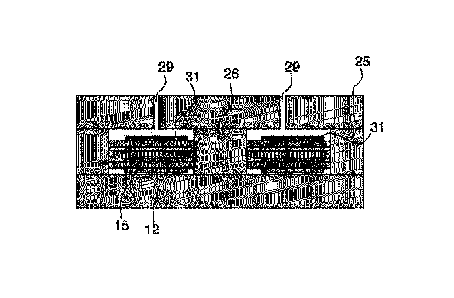
planar magnetic component 5 according to the state of the art. This component
is composed of an electrical circuit 6, consisting of one or more windings 7,
which themselves consist of one or more turns (7-1, 7-2, 7-3, 7-4). The
purpose
of these windings is to produce a magnetic field. This field can be used for
energy storage (inductance) or for transfer (transformer). The component 5
comprises a ferromagnetic core 8, which makes it possible to channel the
magnetic field. This is then referred to as a magnetic circuit. This core 8
can be
produced in several materials depending on the target application
(power/frequency/price/bulk/performance). The core 8 can comprise an air gap
9, a small air space in the circuit, extending parallel to the plane of the
circuit.
[0004] The circulation of the current in the electrical circuit generates
losses in
the same way as the circulation of the magnetic field in the magnetic circuit.
The
losses in the two elements are respectively called copper losses and iron
losses.
Date Recue/Date Received 2022-10-25
2
These losses are interdependent. It is therefore desirable to optimize the
dimensions of each of the elements as a function of the application in order
to
maximize the overall performance levels.
[0005] The invention aims to mitigate all or part of the problems cited
above by
proposing a transformer comprising an innovative electromagnetic component
structure that makes it possible to optimize the performance levels of the
transformer by minimizing the losses, by enhancing the integration of the PCB
(printed circuit board) by limitation of the vies at the periphery of
components, by
limiting the stray inductances and enhancing couplings.
[0006] To this end, the subject of the invention is a transformer
comprising:
- a primary circuit comprising a primary winding of N1 turns of an
electrically
conductive wire, the primary winding extending from an input primary
terminal to an output primary terminal; and
- a secondary circuit comprising a secondary winding of N2 turns of an
electrically conductive wire, the secondary winding extending from an input
secondary terminal to an output secondary terminal, N1 and N2 being each
an integer number greater than or equal to 1;
the transformer being characterized in that it comprises:
- a printed circuit board extending on a first plane, and comprising a
plurality
of layers superposed on one another and forming an aperture through the
first plane around a first axis and defining a perimeter;
- a ferromagnetic core, disposed around the primary and secondary
windings, comprising a central part disposed in the aperture;
- a plurality of vies disposed at the centre of the primary and secondary
windings on the perimeter of the aperture, and extending through the
layers, each on an axis parallel to the first axis, the plurality of vies
being
configured to interconnect the plurality of layers;
in that the N1 turns and the N2 turns of the electrically conductive wire are
each disposed on one of the plurality of layers, according to any alternation
between the N1 turns and the N2 turns, each of the N1 turns and of the N2
turns being wound, from a first via of the plurality of vies, partially around
the
plurality of vies forming a circular arc per layer, to a second via of the
plurality
of vies;
and in that the circular arc of one layer is distinctly oriented with respect
to the
circular arcs of the other layers and has an orientation distinct from the
circular
arcs of the other layers.
Date Recue/Date Received 2022-10-25
3
[0007] Advantageously, the ferromagnetic core comprises an air gap
extending
on a second axis substantially perpendicular to the first plane.
[0008] Advantageously, the input terminals are superposed on the output
terminals on a third axis substantially perpendicular to the first plane.
[0009] Advantageously, at least one out of the plurality of layers is a
shielding
plane, preferentially a ground plane.
[0010] The invention will be better understood and other advantages will
become apparent on reading the detailed description of an embodiment given by
way of example, the description being illustrated by the attached drawing in
which:
[0011] Fig. 1 schematically represents an example of implementation of a
planar magnetic component according to the state of the art;
[0012] Fig. 2 schematically represents an example of disposition, around
the
central vies, of the primary and secondary windings of a transformer according
to the invention;
[0013] Fig. 3 schematically represents an example of vies disposed at the
centre of the primary windings of an inductor according to the invention;
[0014] Fig. 4 schematically represents an example of implementation of the
windings of a transformer according to the invention;
[0015] Fig. 5 schematically represents the variation of the current density
according to a traditional disposition of the air gap and a disposition of the
air
gap according to the invention;
[0016] Fig. 6 schematically represents the induction between the conductors
according to the alternation of the turns of the primary and secondary
windings;
[0017] Fig. 7 schematically represents the homogenization of the current
density in the input and output terminals of the primary and secondary
windings
disposed according to an embodiment of the invention;
[0018] Fig. 8 schematically represents an example of implementation of a
shielding layer in a transformer according to the invention;
Date Recue/Date Received 2022-10-25
4
[0019] Fig. 9 schematically represents a conventional electrical circuit
diagram
of a synchronous rectifier;
[0020] Fig. 10 schematically represents the optimization of the output
terminals
for the synchronous rectification according to the invention.
[0021] In the interests of clarity, the same elements will bear the same
references in the different figures. For better visibility and in the
interests of
improved understanding, the elements are not always represented to scale.
[0022] Figure 1 schematically represents an example of implementation of a
planar magnetic component 5 according to the state of the art and has already
been described in the introduction.
[0023] Figure 2 schematically represents a transformer 10 according to the
invention with an example of disposition, around the central vies, of the
primary
and secondary windings. In this figure, the main elements of the transformer
are
represented by layers (normally superposed). It should be noted that this here
is
an illustration, the number of layers being indicated only as a nonlimiting
example. A person skilled in the art will understand that this number of
layers
can be greater than or less than that of the figure. The transformer 10
comprises
a primary circuit 11 comprising a primary winding 12 of N1 turns of an
electrically
conductive wire, the primary winding 12 extending from an input primary
terminal
13 to an output primary terminal 14. The transformer 10 comprises a secondary
circuit 21 comprising a secondary winding 22 of N2 turns of an electrically
conductive wire, the secondary winding 22 extending from an input secondary
terminal 23 to an output secondary terminal 24 (N1 and N2 each being an
integer number greater than or equal to 1). The transformer 10 comprises a
printed circuit board 15 (broken down in the figure into several layers)
extending
on a first plane 16, and comprising a plurality of layers 17-1, 17-2, 17-3, 17-
4,
17-5, 17-6, 17-7 superposed on one another and forming an aperture 18 through
the first plane 16 around a first axis Z1 and defining a perimeter 19. The
transformer 10 comprises a ferromagnetic core 25 (not represented in this
figure, but intended to be inserted into the aperture 18, and disposed around
the
primary 12 and secondary 22 windings, comprising a central part 26 disposed in
the aperture 18). The transformer 10 comprises a plurality of vies 27 disposed
at
Date Recue/Date Received 2022-10-25
5
the centre of the primary 12 and secondary 22 windings on the perimeter 19 of
the aperture 18, and extending through the layers 17-1, 17-2, 17-3, 17-4, 17-
5,
17-6, 17-7, each on an axis parallel to the first axis Z1, the plurality of
vies 27
being configured to interconnect the plurality of layers 17-1, 17-2, 17-3, 17-
4,
17-5, 17-6, 17-7.
[0024] According to the invention, the N1 turns and the N2 turns of the
electrically conductive wire are each disposed on one of the plurality of
layers,
according to any alternation between the N1 turns and the N2 turns. In other
words, there is one turn (either of the primary winding, or of the secondary
winding) per layer. And the "any alternation" means, in the superpositioning
thereof, one turn of the primary winding can be superposed on one turn of the
secondary winding or of the primary winding. All the combinations of
superposition between primary and secondary can be envisaged. Each of the
N1 turns and of the N2 turns is wound, from a first via of the plurality of
vies 27,
partially around the plurality of vies 27 forming a circular arc 28 per layer,
to a
second via of the plurality of vies 27. In other words, for each layer, the
turn of
the winding (primary or secondary) is not a complete turn, the turn does not
make the 360 around the aperture 18. Thus, a few vies per layer are not
surrounded by said turn. The central disposition of the vies adds great
flexibility
to the positioning of the layers which can be interleaved with respect to one
another, and therefore to the positioning of the turns of the primary winding
and
of the secondary winding.
[0025] Furthermore, the circular arc 28 of one layer is distinctly oriented
with
respect to the circular arcs 28 of the other layers and has an orientation
distinct
from the circular arcs of the other layers. A turn, at the perimeter 19 of the
aperture 18, can be considered to have a first end and a second end in
proximity
to the perimeter. The first and second ends are spaced apart by a certain
number of vies. This spacing between the first and second ends is on each of
the layers, and the respective spacings of the layers are not superposed.
[0026] The transformer according to the invention allows better integration
and
ease of implementation of a shielding in order to limit all the more the
impact of
leakage flux in the vicinity of the air gap. The minimization of the induction
at the
Date Recue/Date Received 2022-10-25
6
interconnections makes it possible to reduce the losses. All these aspects and
advantages of the invention are detailed hereinbelow.
[0027] Figure 3 schematically represents an example of vies 27 disposed at
the centre of the winding 12 of an inductor 10 according to the invention. In
this
illustration, it must be considered that the diagram (b) is repeated six times
and
offset each time. The result thereof is an inductor with 7 turns of an
electrically
conductive wire (therefore N1 = 3), implemented on 8 layers (once again, only
three layers are represented for better legibility of the figure). The winding
12
extends from the input primary terminal 13 to the output primary terminal 14.
[0028] The use of vies at the centre of the magnetic component allows for a
simplified production of the various windings. For that, it is possible to
reproduce
an elementary winding on each of the layers (b) in order to produce the
desired
winding. A single turn is produced per PCB layer. The transition between the
different layers is obtained via the central vies 27. One or more vies can be
used
for this purpose depending on the current desired in the windings and the size
of
the core 25 (and its central part 26).
[0029] This configuration of one turn per layer runs counter to the known
practices. In fact, normally, in power electronics, the number of turns is
spread
out on a single layer (as shown in Figure 1). The fact of considering one turn
per
layer here necessitates a large number of PCB layers if the aim is to produce
a
large number of turns. On the other hand, the fact that the vies are placed at
the
centre, on the perimeter of the aperture, makes it possible to reduce the
layer-to-
layer access resistances and frees up space at the periphery of the component,
which allows better integration.
[0030] Figure 4 schematically represents an example of implementation of
the
primary 12 and secondary 22 windings of a transformer 10 according to the
invention. More specifically, the output winding is incorporated in the ring
of
central vies 27. In order to interleave the primary and secondary windings,
here
again the vies allowing the interconnections between the layers 17 are
themselves also interleaved. The turns of the secondary winding can be each
inserted between two turns of the primary winding and/or between one turn of
the primary winding and one turn of the secondary winding. This configuration
is
Date Recue/Date Received 2022-10-25
7
advantageous for a transformer since it allows a better integration and
facilitates
the implementation of a shielding in order to limit as far as possible the
impact of
the proximity effects (and only in the case where the component has an air
gap).
The minimization of the induction at the interconnections allows reduction of
the
losses.
[0031] Figure 5 schematically represents the variation of the current
density
according to a traditional disposition of the air gap (on the left of the
figure) and a
disposition of the air gap according to the invention (on the right of the
figure).
This representation is based on an illustration taken from the Schafer 2018
publication Optimal Design of Highly Efficient and Highly Compact PCB Winding
Inductors. According to the invention, the ferromagnetic core 25 comprises an
air gap 29 extending on a second axis Z2 substantially perpendicular to the
first
plane 16. The use of a vertical air gap 29 is made possible by the machining
of
the existing cores or of raw material. In the trade, the planar cores more
often
than not have an air gap disposed on the central leg which makes the field
radiate in a direction parallel to the planar windings (see left-hand
illustration).
The configuration on the left of the figure represents a copper conductor at
the
centre subjected to leakage fields emanating from the two air gaps in the
magnetic core. The current densities are concentrated on the edges of the
conductor which reduces the efficiency of the solution. More specifically, in
a
traditional disposition of the air gap (called horizontal), the magnetic field
is
propagated in the core. At the air gap, the field lines radiate around the air
gap
and these field lines tend to concentrate the currents circulating in the
conductor
to the outside, so much so that the current circulates only on the outside,
where
the field lines are concentrated. In other words, only a small part of the
conductor is actually used. In the configuration on the right of the figure,
corresponding to the invention, the leakage fields arrive perpendicular to the
conductor which allows the current density and therefore the losses to be
reduced. More specifically, in a vertical disposition, the field radiates
perpendicular (see right-hand illustration), which reduces the effects of
proximity
to the core and therefore reduces the concentration of current, at the ends,
in
the electrical circuit. The currents are concentrated on the surface and all
of the
Date Recue/Date Received 2022-10-25
8
conductor is used. The result thereof is a positive impact on the radiation.
Thus,
the resistance of the winding is reduced.
[0032] Figure 6 schematically represents the induction between the
conductors
according to the alternation of the turns of the primary and secondary
windings.
In the bottom part of the figure, the conductors in a planar transformer are
represented. The layers annotated P1 represent the primary conductors while
the layers annotated S1 represent the secondary conductors. In the left-hand
part of the figure, the turns of the primary winding and the turns of the
secondary
winding are disposed alternately, and the choice of the mode of alternation is
facilitated according to the invention. In the right-hand part of the figure,
the
turns of the primary winding and the turns of the secondary winding follow one
another, with no alternation between the primary and secondary windings. On
the same diagram, the profile of the theoretical induction is given (H). The
induction between the conductors increases the concentration of the currents
therein, which increases the losses. It can be seen that, without alternation,
the
maximum induction obtained is greater than the maximum induction obtained in
the case of a transformer according to the invention (with alternation of the
turns). That generates a lot of losses by conduction between the two central
layers (P1 and S1) which have a much greater resistance.
[0033] Figure 7 schematically represents the homogenization of the current
density in the input and output terminals of the primary and secondary
windings
disposed according to an embodiment of the invention. This representation is
based on an illustration from the Schafer 2018 publication Optimal Design of
Highly Efficient and Highly Compact PCB Winding Inductors. In this embodiment
of the invention, the input terminals 13,23 are superposed on the output
terminals 14, 24 on a third axis Z3 substantially perpendicular to the first
plane
16, as can be seen in the top right part of the figure. That makes it possible
to
avoid the phenomena of field concentration between the two planes. With the
terminals positioned in two different parallel planes, the current is more
distributed throughout the plane and not only concentrated in the middle of a
single plane. The bottom part of the figure represents the results of a
simulation
by finite elements of the current density with adjacent terminals (on the left
of the
Date Recue/Date Received 2022-10-25
9
figure) and superposed terminals according to the invention (on the right of
the
figure).
[0034] It emerges therefrom that the interleaving of the conductors makes
it
possible to reduce the induction between the conductors and therefore the
concentrations of current. A disposition of the terminals vertically makes it
possible to homogenize the current densities and therefore reduce the losses
in
the terminals.
[0035] Figure 8 schematically represents a cross-sectional view, in a plane
perpendicular to the first plane 16, of an example of implementation of a
shielding layer in a transformer according to the invention. In one embodiment
of
a transformer of the invention, at least one out of the plurality of layers 27
is a
shielding plane 31, preferentially a ground plane. The shielding plane
concentrates the eddy currents which generate losses. Thus, by virtue of the
shielding plane, these losses are generated in the shielding plane and no
longer
in the windings. The aim is to limit the total losses. The equivalent
resistance of
the circuit depends on the different resistances in the circuit. With
shielding
plane, this resistance is reduced.
[0036] The shielding plane 31 is most often a ground plane. The leakage
field
creates in this plane an induced current (eddy current) which generates losses
therein. The distance from the shielding to the air gap, the thickness of the
shielding and the distance from the shielding to the conductor depend on the
power involved, on the operating frequency (and form of the signals), and on
the
performance sought with respect to the integration of the component.
[0037] In the general case, the implementation of the solution is
profitable if it
makes it possible to reduce the total losses. In a particular case of use that
is the
resonant converter, the reduction of the equivalent resistance of the
conductors
is a factor to be taken into account. Limiting this resistance makes it
possible to
facilitate the primary resonance and therefore the soft switching. In this
particular
case, it will therefore also be necessary to take account of the saving made
by
this operation on the magnetic dimensioning.
[0038] The invention makes it possible to enhance the overall performance
of
a planar magnetic component by a set of characteristics with many advantages:
Date Recue/Date Received 2022-10-25
10
- The disposition of the vies at the centre in order to produce the
interconnection of the different layers, in particular in the case of the
transformer with the vies of the primary and secondary windings and a
flexibility in the choice of interleaving (that is to say interleaved between
one
another);
- The presence of a shielding plane associated with a vertical air gap
which
makes it possible to limit the effect of the leakage fluxes on the conductors.
In a resonant configuration, this advantage is all the more exploitable;
- The optimization of the output terminals to enhance the synchronous
rectification. This advantage is exploited above all in the converters with
high
output current and high operating frequency necessitating the use of one or
more GaN transistors.
[0039] Figure 9 schematically represents a conventional electric circuit
diagram of a synchronous rectifier. In this figure, on the left is represented
the
transformer (ideal coupler), Rs represents the spurious series resistance of
the
secondary winding and of the routing, QR the synchronous rectification
transistor, DQR and CQR the spurious components associated with this
transistor, Cout and Rout represent the output capacitance of the converter
and
the load respectively.
[0040] In the example that will now be dealt with, only two planes make it
possible to produce the secondary winding. It is possible to imagine a
different
configuration in order to optimize the performance levels (more copper on the
secondary means less losses).
[0041] Figure 10 schematically represents the optimization of the output
terminals for the synchronous rectification according to the invention. As
described previously, the winding can be produced by using one group of vies
in
every two. Through the optimization of the terminals of the transformer, it is
possible to improve the integration of the secondary in order to minimize the
losses in the synchronous rectification. Generally, a lowering of voltage
between
the primary and the secondary is applied. The result thereof is a voltage at
the
secondary that is lower than at the primary. That also means stronger currents
on the secondary. It is desirable to minimize the resistance on the secondary
Date Recue/Date Received 2022-10-25
11
terminals to optimize the performance levels. In the figure, the path of the
current is minimized to the output.
[0042] This enhancement leads to a reduction of the resistance Rs and of
the
spurious inductances at the secondary. Furthermore, it allows an easier
increasing of the number of transistors at the synchronous rectification,
which
makes it possible to even further reduce the losses.
[0043] Finally, it is thus possible to place the drivers as close as
possible to the
transistors, a critical point for GaN transistors for example.
[0044] It can be stressed that the optimization of the various parameters
of the
magnetic components discussed above is adaptable to most of the converter
configurations.
[0045] Thus, the invention comprises a number of technical features, that
can
be combined with one another, the technical effects of which are listed below:
[0046] - Use of vies disposed at the centre of the planar (close to the
central
part). This configuration allows an easier distribution of the different
windings
without penalizing the integration outside the component. This disposition
further
allows a simplified interleaving of the layers.
[0047] - Use of a machined air gap on the top of the magnetic core.
Contrary to
a horizontal disposition of the air gap, a vertical disposition orthogonal to
the
windings makes it possible to limit the effects of proximity to the windings
and
therefore reduces the copper losses above all at high frequency (> 500 kHz).
[0048] - Interleaving/superpositioning of the terminals on a vertical
plane. The
interleaving makes it possible to reduce the induction and therefore the
strong
concentrations of current. The vertical disposition makes it possible to use
the
total section of the planar conductors and therefore reduce the AC resistance.
[0049] - Use of shielding planes. Situated as close as possible to the air
gap,
they make it possible to limit the effects of proximity on the conductors. The
vertical disposition of the air gap associated with the shieldings minimizes
the
effects of the air gap on the conductors.
[0050] - Optimization of the terminals for the integration of the GaN
transistors.
Since synchronous rectification operates at high frequency and high current,
it is
Date Recue/Date Received 2022-10-25
12
necessary to limit the spurious inductances and resistances at the secondary.
An interleaved and optimized disposition of the secondary makes it possible to
increase the performance levels of this type of system.
[0051] It will
appear more generally to the person skilled in the art that various
modifications can be made to the embodiments described above, in light of the
teaching which has just been disclosed to him or her. In the following claims,
the
terms used should not be interpreted as limiting the claims to the embodiments
explained in the present description, but should be interpreted to include
therein
all the equivalents that the claims aim to cover by virtue of their
formulation and
the anticipation of which is within the scope of the person skilled in the art
based
on his or her general knowledge.
Date Recue/Date Received 2022-10-25