Note: Descriptions are shown in the official language in which they were submitted.
WO 2021/237362
PCT/CA2021/050723
1
QUANTUM ANALOG COMPUTING AT ROOM TEMPERATURE USING
CONVENTIONAL ELECTRONIC CIRCUITRY
CROSS-REFERENCE TO RELATED APPLICATIONS
[0001]
This application claims the priority or benefit of U.S. provisional
patent application 63/032,426, filed May 29, 2020, the specification of which
is
hereby incorporated herein by reference in its entirety.
BACKGROUND
(a) Field
[0002]
The subject matter disclosed generally relates to quantum computing
devices. More specifically, it relates to a quantum analog device comprising
analog
electronic devices working at room temperature to carry out computations by
exploiting certain quantum effects.
(b) Related Prior Art
Quantum Computing
[0003]
Quantum mechanics was successfully applied in a variety of
domains to improve our understanding about polymers, semiconductors,
superfluids, superconductors, among many others. In 1982, Richard Feynman
pointed out that some quantum mechanical effects cannot be efficiently
simulated
on a classical von Neumann architecture [1]. This, in turn, led to the
proposal that
one can perform more efficient computations if quantum effects are harnessed,
leading to quantum computers [2]. Works by Feynman [1], Manin [2], Pople [3],
Kohn [4], Deutsch [5], and others, conveyed that to simulate quantum mechanics
on von Neumann computers would necessitate exponential growth of hardware
resources with the growth of the problem size, making certain problems
incapable
of simulation. Those difficulties could be possibly circumvented by a quantum
computer. In a very general sense, with quantum computing, one tries to solve
problems by exploiting quantum effects to inspect computational correlation
and
then reach a correct answer through effective interference.
CA 03180580 2022- 11- 28
WO 2021/237362
PCT/CA2021/050723
2
[0004]
Several quantum computing paradigms have been introduced which
come with different advantages and disadvantages. The most widely known one
is the gate paradigm which is analogous to the binary logic gates in classical
computers. Quantum information is processed by means of quantum gates,
implementing complex circuits to achieve practical functionalities with the
promise
of incredible advantages over classical computing. But gates are not the only
way
to realize quantum computing. In adiabatic quantum computing [23], the
computation starts from an initial Hamiltonian with an easy-to-construct
ground
state. The Hamiltonian is then gradually varied into a final Hamiltonian,
whose
ground state encodes the solution to the computational problem. The adiabatic
model is pursued on the theory that the architecture may have a certain
inherent
fault tolerance [24,25,26] due to resistance to slowly varying control error.
Moreover, the energy gap may provide inherent resistance to noise, due to
stray
couplings to the environment, for example, if noiseless qubits are developed
[25].
It has been theoretically shown that adiabatic quantum computing is as
powerful
as the circuit-based approach, but it brings with it a significant cost in
terms of
additional physical qubits (just like in the gate paradigm).
[0005]
The architectures described above can be realized with various
physical objects acting as qubits [36]. Examples include trapped ions [37],
quantum dots, cavity QED [38], neutral atoms, superconducting electrical
circuits
wherein many electrons are moving [39], and liquid and solid state nuclear
magnetic resonance [40], among others.
[0006]
The realization of practical quantum computing is dependent on the
development of better (noiseless) qubits, better interconnects, improved
control,
and error correction. For its part, error correction is governed by the
threshold
theorem which involves three main assumptions: 1) errors occur independently
(on
qubits, gates and measurements), with no spatial or temporal correlations; 2)
one
can perform many gates simultaneously on physical qubits; and 3) the noise is
brought under a certain threshold with quantum error correction algorithms
such
CA 03180580 2022- 11- 28
WO 2021/237362
PCT/CA2021/050723
3
that even when more qubits are added, one can eliminate error faster than it
is
created, clearing the road for the quantum computer to emulate a perfect
quantum
system. As a result, one can perform accurate computations with hundreds of
digits after the decimal. Since it will be capable of dealing with such
numbers
efficiently (something digital computers, above a certain digit, cannot), a
quantum
computer can in theory solve problems computationally intractable with digital
computers. At the current moment, no such fault-tolerant quantum computation
has been achieved.
SUMMARY
[0007]
According to a first aspect, there is provided quantum analog
computing device, or an integrated circuit for quantum analog computing, the
integrated circuit comprising:
a plurality of qubits connected to each other, each qubit of the
plurality of qubits comprising resistors, inductors, capacitors and a switch,
wherein the qubits are connected to each other according to a connectivity
topology that provides an analog of quantum behavior at room temperature.
[0008]
According to an embodiment, the connectivity topology is a Hopfield
network.
[0009]
According to an embodiment, each qubit in the Hopfield network is
connected to all other qubits of the Hopfield network.
[0010]
According to an embodiment, the qubits are connected to each other
using at least one of: an inductor and a capacitor.
[0011]
According to an embodiment, each qubit comprises a metal oxide
semiconductor (CMOS)
[0012]
According to an embodiment, the qubits are operating at a room
temperature.
CA 03180580 2022- 11- 28
WO 2021/237362
PCT/CA2021/050723
4
[0013]
According to an embodiment, the qubits are operating at a
temperature of between 0 and 30 degrees Celsius.
[0014]
According to an embodiment, each qubit of the plurality of qubits
corn prises:
a first resistor, a voltage source, a first inductor, a first capacitor, and
a shunt capacitor connected in a first series circuit, the shunt capacitor
having
a first node on one side and a second node on another side; and
the switch, a second resistor, a second inductor, and a second
capacitor connected in series and forming a second series, the second series
being connected in parallel to the shunt capacitor at the first node and the
second node.
[0015]
According to an embodiment, the voltage source is controlled to set
each qubit with a particular initial state.
[0016]
According to an embodiment, the integrated circuit is operable to
reach a stable state, the integrated circuit measuring a voltage on each qubit
to
determine the voltage of each qubit associated to a current state in order to
perform
computation.
[0017]
According to another aspect, there is provided a method comprising
the steps of:
providing and connecting a plurality of qubits connected to each
other according to a connectivity topology which is an all-to-all topology,
each
qubit of the plurality of qubits comprising resistors, inductors, capacitors
and
a switch to be equivalent to an atomic qubit;
setting an initial voltage of each qubit of the plurality of qubits; and
operating the plurality of qubits at the room temperature to reach a
final state representative of a solution to a given problem and measuring an
CA 03180580 2022- 11- 28
WO 2021/237362
PCT/CA2021/050723
associated voltage of each one of the plurality of qubits to perform quantum
analog computation to determine the solution.
[0018]
According to an embodiment, there is further provided a step of
operating amplifiers used to connect the qubits by the connectivity topology.
[0019]
According to an embodiment, connecting the plurality of qubits
according to the connectivity topology comprises connecting the plurality of
qubits
according to a Hopfield network built with resistors and capacitors.
[0020]
According to an embodiment, each qubit in the Hopfield network is
connected to all other qubits of the Hopfield network.
[0021]
According to an embodiment, providing and connecting a plurality of
qubits comprises connecting each qubit to all other qubits of the plurality of
qubits
using at least one of: an inductor and a capacitor.
[0022]
According to an embodiment, each qubit comprises a metal oxide
semiconductor (CMOS).
[0023]
According to an embodiment, the qubits are operated at a
temperature between 0 and 30 degrees Celsius.
[0024]
According to an embodiment, each qubit is connected to a plurality
of other qubits and all qubits participate in calculation, such that no qubit
is used
for error correction.
BRIEF DESCRIPTION OF THE DRAWINGS
[0025]
Further features and advantages of the present disclosure will
become apparent from the following detailed description, taken in combination
with
the appended drawings, in which:
[0026]
Fig. 1 is a schematic diagram illustrating a circuit used to provide a
classical circuit analog to electromagnetically induced transparency (EIT),
according to an embodiment of the invention;
CA 03180580 2022- 11- 28
WO 2021/237362
PCT/CA2021/050723
6
[0027]
Fig. 2 is a schematic diagram illustrating a coupled RLC circuit used
to model a 4-level atomic system, where R1,2,3, C1,2,3, L3 and Vs1,s2 are
resistors,
capacitors, inductors and alternating voltage sources, respectively, and
capacitor
C is shared between loops 1-3 and 2-3, according to an embodiment of the
invention;
[0028]
Fig. 3 is a schematic diagram illustrating a network of qubits (in
green, left half of the network graph) which are fully connected between
themselves and the ancilla (in red, right half of the network graph) connected
to
every qubit through coupling (gates), according to an embodiment of the
invention;
[0029]
Fig. 4 is a schematic diagram illustrating an electric circuit
corresponding to equation 10 (described further below), with fast amplifiers,
according to an embodiment of the invention;
[0030]
Fig. 5 is a schematic diagram illustrating an electric circuit modeling
a neural circuit with electrical components, where the neuron outputs can be
connected to the input of any neuron (the black squares in this case represent
resistive connections between the outputs and inputs; the circles in the
amplifiers
represent connections from inhibitory connections), according to an embodiment
of the invention;
[0031]
Fig. 6 is a schematic diagram illustrating an electric circuit embodying
a 4-bit analog-to-digital converter (ADC) computational network, where the
input is
analog, while the digital representation of the input is V3, V2 V1, Vo and is
carried
out as a binary value from the output amplifier voltage, according to an
embodiment of the invention;
[0032]
Fig. 7 is a schematic diagram illustrating the Chimera graph created
by D-Wave comprising an NxN grid of unit cells with eight qubits per cell,
fully
interconnected within the cell, and longitudinally coupled to four other
qubits,
according to the prior art;
CA 03180580 2022- 11- 28
WO 2021/237362
PCT/CA2021/050723
7
[0033]
Fig. 8 is a schematic diagram illustrating the Q5 coupling map, by
IBM, according to the prior art;
[0034]
Fig. 9 is a schematic diagram illustrating an electronic
semiconductor-based qubit, or "CMOS Qubit", comprising a combination of
resistors, capacitors, inductors and a switch, according to an embodiment of
the
invention;
[0035]
Fig. 10 is a schematic diagram illustrating CMOS Qubits connected
together in a connectivity topology according to a network which, at run time,
performs quantum analog computing, according to an embodiment of the
invention;
[0036]
Fig. 11 is a flowchart illustrating a method for operating an electronic
semiconductor-based qubit, or "CMOS qubit", comprising a combination of
resistors, capacitors, inductors and a switch, to perform quantum analog
computing, according to an embodiment of the invention;
[0037]
Fig. 12 is a flowchart illustrating a method for operating an electronic
semiconductor-based qubit, or "CMOS qubit", connected according to a
connectivity topology, according to an embodiment of the invention;
[0038]
Figs. 13A-13B are graphs illustrating a comparison of simulated and
experimental results of Rabi oscillations observed during the simulation or
experiment for different values of the circuit representing the pump laser,
and the
Fourier transform thereof, according to an embodiment of the invention;
[0039]
Fig. 13C is a diagram illustrating an atomic system undergoing laser
pumping and to which the analog circuit operated to arrive at the results of
Figs. 13A-13B is an analog;
[0040]
Figs. 14A-14B are graphs illustrating a comparison of the time to
perform the traveling salesperson problem with a growing number of "cities",
CA 03180580 2022- 11- 28
WO 2021/237362
PCT/CA2021/050723
8
between a device operated according to an embodiment of the invention and a
benchmark using Gradient Descent on a "normal" computer;
[0041]
Fig. 15 is a graph illustrating a comparison of the time to solve the
Black-Sholes model with a growing number of price points, between a device
operated according to an embodiment of the invention and a benchmark using a
classical stochastic optimization method on a "normal" computer; and
[0042]
Fig. 16 is a set of graphs illustrating, in relation with the example of
Fig. 15, the accuracy of the quantum analog results compared to CMAES results
and implicit method for the Black Scholes model for 10 (upper left plot), 50
(upper
right plot), 100 (lower left plot), and 200 (lower right plot) price points.
[0043]
It will be noted that throughout the appended drawings, like features
are identified by like reference numerals.
DETAILED DESCRIPTION
Analog Computation
[0044]
Analog computation refers to an analogy ¨ or a systematic
relationship ¨ between the physical processes in the computing device and
those
in the system it is modeling/describing. An analog computer is therefore an
analog
of the particular system it is set to describe [34], [35]. For instance,
electrical
quantities such as voltage, current, conductance can be used as analogs for
fluid
pressure, flow rate, and pipe diameter of a hydraulic system. Stated
differently, the
physical quantities of the analog device follow the same mathematical laws as
the
physical quantities in the system under study. While the dynamics of an analog
computer typically perfectly matches the dynamics of the original system [36],
it is
also true that different devices or systems can be analogs of one another
without
necessarily having any physical resemblance [34].
[0045]
In analog computers, rather than operating through the
manipulations of numbers as digital computer do, numbers emerge as a result of
measurements of physical parameters. Analog computers use continuously
CA 03180580 2022- 11- 28
WO 2021/237362
PCT/CA2021/050723
9
adjustable quantities of the system in order to codify a given problem. The
time
evolution of the voltage waveform of the analog computer represents the
encoding
of the solution of a given problem. Electronic components (physical devices)
are
used to sum, multiply, and integrate physical quantities like these signals.
These
components are connected in a way that the voltages of the analog computer are
related by the same mathematical equations as the original physical variables.
Some of the basic components of an analog system are amplifiers,
potentiometers,
multipliers and function generators through which one can carry out
mathematically operations such as addition, subtraction, multiplication,
division,
integration, and so on. One of the advantages of analog systems is the ability
to
connect these components in a variety of ways, depending on the physical
system
under consideration. A key technological development leading to the wider
adoption of analog computations was the alternating and direct current
operational
amplifier, which can perform mathematical operations such as addition,
subtraction, integration and differentiation electronically.
[0046]
Two main considerations were used for evaluating the computation
on analog computers: accuracy and precision. Accuracy pertains to the
relationship between the simulation and the primary system being simulated, or
put another way ¨ the relationship between the computational result and the
mathematical correct results. Precision is, on the other hand, a stricter
notion,
referring to the quality of the computing device and is typically dependent on
the
resolution (quality of operation) and stability (lack of drift). Therefore, by
a precision
of 0.01% one understands that the results will be bound within 0.01% of the
represented value for a reasonably long period of time. In order to compare
analog
devices, one usually expresses precision as the difference between the maximum
and minimum representable values. Multiple factors affect accuracy and
precision.
These factors include the choice of physical process, the set-up of the
machine,
as well as the physical effects (loading, leaking and other losses) - the
quality of
the resistors or capacitors and other components used to construct the
machines.
CA 03180580 2022- 11- 28
WO 2021/237362
PCT/CA2021/050723
Noise affects the system as well, and it can be intrinsic (e.g. thermal noise)
as well
as extrinsic (e.g., ambient radiation). There are several advantages of analog
computers, including speed, inherent natural parallelism, and small size.
These
advantages stem from the fact that analog computations are close to the
physical
processes that realize them. In principle, any mathematically described
physical
process can be used for analog computation.
[0047]
Analog computers have a long history prior to the digital age, and
have been applied to an extensive variety of fields. While, for the last 50
years,
digital computing has been the dominant paradigm, with the slowing down of
Moore's law, several non-Von Neumann hardware architectures have emerged
such as: analog memory [37], neuromorphic photonics [38] ,[39], optical co-
processors [40], as well as quantum computing to tackle complex tasks more
efficiently than digital processors.
[0048]
An interesting perspective on the field of quantum computing was
raised by D. Ferry in 2001 where the role of the use of parallel analog
computation
for speed gain was discussed. Ferry examines a qubit as a analog quantity,
showing that in certain processes the real speed up comes from the analog
quantities and advantages and "not from the use of quantum mechanics". Kish,
taking inspiration from the same paper, has pro-posed a quantum computing
approach via Hilbert space computing with analog circuits [42], an approach he
calls a Hilbert-space-analog (HSA) computer.
[0049]
Analog computer has been defined as devices used to solve a
mathematical problem with respect to a primary physical system. This is due to
the
same, or related mathematical structures for both the computational and
primary
(physical) systems. Even though, from a practical standpoint, certain analog
systems are better suited than others, in principle any physical system can be
used
as long as it obeys the same equations as the primary system. As such the
analog
device can be used to demonstrate quite clearly multiple facets of the
mathematics
of quantum mechanics since an analog device computes by exploiting physical
CA 03180580 2022- 11- 28
WO 2021/237362
PCT/CA2021/050723
11
phenomena directly. This idea was also supported by Feynman, who showed one
can reduce an exponentially complex problem of calculated probabilities to one
of
polynomial complexity of simulated probabilities. Therefore, in the case of NP
complete problems one can create such a physical system, which mathematical
description corresponds to those of the specific NP problem. Thereupon, such a
physical system can be realized through appropriate analog device, which is
able
to simulate the corresponding NP-complete problem. The reason for the growing
attraction of quantum computing comes from its analog nature, which is based
on
physical simulations of quantum probabilities.
[0050]
Taking into account the nature of computation, as well as the analogy
between physical systems, realized in terms of analog computational devices, a
new way to perform computation is proposed herein, called quantum analog
computing. It is analog in two ways. First, it relies on analogies with
quantum
systems (i.e., the computing arrangement has the same behavior as the "real"
system being modeled, as described above). Second, it employs analog
electronics. In practical terms, this means that instead of dealing with
actual atoms
or molecules to carry out quantum computations (which are extremely
sensitive),
analog circuits based on basic electronic elements (for example CMOS-based)
can be used to achieve some quantum computing capabilities.
[0051]
There is described below a method for performing quantum analog
computing (including, without limitation, tasks such as quantum annealing)
with
conventional electronics. Each conventional electronic computational structure
(qubit) having the following basic elements: resistors, capacitors, inductors
and a
switch or their equivalent is capable of working at room temperature and is
now
referred to hereinafter as a "CMOS Qubit". The commercial term "Qsistor" may
be
used as a trademark. These CMOS Qubits are connected together in a particular
way (a connectivity topology) described further below. More specially, this
can be
a CMOS chip composed of qubits designed and controlled through conventional
electronic circuitry.
CA 03180580 2022- 11- 28
WO 2021/237362
PCT/CA2021/050723
12
[0052]
The analog circuits (qubits), connected by an all-to-all connectivity,
allow the problem to be codified into the topology of the device. The
computation
proceeds until a stationary regime is reached. The stationary regime
represents
the solution of the problem. According to an embodiment, and as detailed
further
below, the qubits can be connected according to a Hopfield network to perform
such a task.
[0053]
For example, Fig. 14 is a schematic diagram illustrating qubits, such
as CMOS qubits, connected together in a connectivity topology according to a
network which, at run time, performs quantum analog computing, according to an
embodiment of the invention. Each qubit on one side is connected to each qubit
in
the other side, although this is a non-limiting representation. Other
representations
would be possible, such as a circle. According to an embodiment, the topology
of
connections implements the all-to-all connectivity by which all qubits
participate in
calculations.
[0054]
As they use conventional electronics, connected CMOS qubits are
operable at room temperature, as an integrated circuit device. According to an
embodiment, the room temperature which is the temperature of the environment
in which the computer is operated is typically between -10 C and 40 C, more
specifically between -5 C and 35 C, more specifically between 0 C and 30 C,
more specifically between 15 C and 25 C.
[0055]
Moreover, due to the system's individual components as well as the
connectivity type, the system does not require any error correction and all
available
qubits participate in the computational process. Also, since the system is
built from
traditional CMOS type equipment, the architecture allows significant
scalability,
allowing thousands of qubits in the system than what is currently possible in
the
industry nowadays, where this number is still limited due to many practical
considerations such as the need for cryogenic technology, which is not
required in
the system described herein below.
CA 03180580 2022- 11- 28
WO 2021/237362
PCT/CA2021/050723
13
[0056]
Since there is no need for cryogenic technology and since all
available qubits participate in the computational process (i.e., none is
needed for
error correction), the circuitry and its environment are made much simpler
than
currently available technology, with the advantage of permitting rapid changes
in
circuitry. Changes in circuitry need to be made to perform different computing
tasks. Making these circuitry changes rapidly is an advantageous result of
using
the system described herein to perform quantum analog computing.
[0057]
There are now described the foundational aspects on which the
quantum analog computing device according to the invention is built, such as
the
qubit, followed by a description of carrying out certain quantum effects
through
classical electronic circuitry according to the invention.
Foundational aspects
1. Qubit - definition
[0058]
In this section, there is provided a general description of the basic
computational structure (qubit). In classical information processing,
operations are
performed using bits. Those are two-state systems, with the states being 0 and
1.
By grouping those binary bits together we can represent information, while the
manipulation of those bits allows classical computers to carry out arbitrary
computations. Respectively a bit can be represented as a switch which is
either on
or off. Correspondingly, in a quantum system the fundamental element in
quantum
information is the quantum bit, also known as qubit. A qubit is a unit vector
of a
two-dimensional vector space which represents particular basis states (two or
more discrete energy states) such as 10) or 11).
[0059]
In a contrast to a classical bit which can have two states, 0 and 1, a
qubit can be in a superposition state (If = cos(61/ 2)10) + eiOsin(19 /2)11),
which
corresponds to the classical version of the bit states. In a quantum computer,
qubits represent the encoding of information, and those qubits require strong
interaction with one another. Compared to classical information system, qubits
are
CA 03180580 2022- 11- 28
WO 2021/237362
PCT/CA2021/050723
14
not confined to two states and instead can be found in arbitrary superposition
states. When exploiting the superposition states to carry out information
processing, where a state can be described as
VI) = al0) + fill) (1)
with a and )6' being complex numbers, qubits become more powerful than their
classical equivalent (bit).
[0060]
Another key property is entanglement, where qubits interact with one
another in a way that following that interaction, they cease to be
independent. For
instance, the Bell state, describing entanglement such as
ICY) = 71 (100) +111)) (2)
[0061]
There is zero probability of observing 101) or 110), while the
probability of 100) and 111) are each 1/2. Due to entanglement the
probabilities of
multi-qubit states cannot be separated into product of individual
probabilities.
Importantly entanglement can be achieved between physically separated
particles,
and it can be preserved in time and through transformations and measurements.
[0062]
The completion of a quantum computation through qubits, requires
the measurement (read out) of the state of the qubit. When this state of a
qubit is
measured, the quantum nature of the qubit is momentarily lost, meaning the
superposition of the basis states breaks down to either 10) or 11)., thus
becoming
similar to a classical bit. This naturally leads to the tradeoff between
control and
coupling in order to preserve quantum coherence.
[0063]
While the power of classical information processing stems from the
manipulation of a groups of bits (depending on the particular paradigm), in
quantum computation the advantages become evident in a system with two or
more qubits. Those qubits can be physically realized in different ways - e.g.,
a
single photon (particle of light), a single atom or a single electron, etc.
Multiqubit
operations have been introduced from different implementations such as
CA 03180580 2022- 11- 28
WO 2021/237362
PCT/CA2021/050723
superconducting qubits [7, 8, 9], trapped-ion [10, 11, 12], solid-state spin
[13, 14],
nuclear spin [15], neutral atom [16, 17]. The coherence times in those systems
are
varied and often represent a serious limitation for those architectures.
[0064]
Peter Shor was the first to propose a quantum error correction
mechanism, where quantum information is redundantly encoded by its
entanglement within a larger system of qubits [21], providing error correction
during
quantum computation. Therein, as previously mentioned two types of qubits are
necessary ¨ physical qubits performing computation and extra qubits, known as
ancillas, which are utilized to detect errors before they accumulate.
Therefore,
multiple physical qubits are to be connected in a large network in order to
operate
a single logical qubit [22], that perform the computation at hand. This is an
extremely important barrier in the capability of constructing a large-scale
quantum
machine. As shown in Fig. 3, for N qubits there would be N2 ancilla,
necessitating
N ¨ 1 and 2N ¨ 3 couplers (gates).
[0065]
Compared to prior art quantum computing devices that need specific
hardware and software error correction functionality, the quantum analog
computing device according to an embodiment as described herein does not
require any type of error correction functionality, since the device does not
suffer
from errors accumulating over time due to noise. The quantum analog computing
device as described herein does not require additional qubits to serve as an
error
correction and, as a result, all available qubits, which can be in an all-to-
all
connectivity, participate in the computational process.
2. Analogy between quantum two-state systems and specific classical systems
[0066]
Although today we consider the SchrOdinger equation as the
standard quantum mechanical formalism, it is worth noting that it was
developed
on the basis of classical optical ideas [41].
[0067]
In fact, throughout the history of science, researchers have relied on
analogies to provide insights into unfamiliar concepts, systems, objects or
events
CA 03180580 2022- 11- 28
WO 2021/237362
PCT/CA2021/050723
16
by considering the properties of an already known counterpart. In the case of
quantum-classical wave analogies, two effects - one in a quantum system and
another in a classical wave, represent different manifestation of the same
underlying physical principles (the wavefunction of a photon corresponds to
the
classical electromagnetic field) [42], [43]. Much as in the early days of
quantum
mechanics scientists relied on those analogies to convey their knowledge of
electromagnetism to the emerging theory, today, quantum-wave analogies are
often used to provide an intuition in the investigation of new phenomena in
classical waves.
[0068]
There are a multitude of classical-classical, quantum-quantum, and
quantum-classical analogies which are well known and accepted by the physics
community for decades. In the current section, we are going to focus on the
quantum-classical analogies specifically. Many classical-classical analogies
exist.
For instance: mechanics and electricity [44], inertial and electromagnetic
forces
[45], or mechanical system corresponding to phase transitions in a one
dimensional medium [46]. Similarly there are many quantum-quantum analogies.
Some quantum systems have classical analogs only in phase space, in other
cases quantum states described by the SchrOdinger equation are propagating
through specific structures in the exact same way as electromagnetic fields
propagate through optical structures. Another example is the quantum states
defined by a Dirac-like equation that have analogs to optical fields
propagating
through special materials (e.g., graphene [47]).
[0069]
One of the most incontrovertible evidence is the analogy between
electron waves in a quantum waveguide and electromagnetic waves, allowing a
variety of microwave device concepts to be used in developing quantum devices
[48]. Several structures, based on such analogy have been already utilized,
such
as stub-tuning device [49], [50], cavity coupled to two quantum waveguides
[51],
and double-bend quantum waveguide [52]. An interesting case of electromagnetic
waves and quantum wave functions analogy is the electron interference in solid-
CA 03180580 2022- 11- 28
WO 2021/237362
PCT/CA2021/050723
17
state devices. Devices include Fabry-Perot interference filters for electrons
[53],
narrow band pass interference filters [54], Butterworth equal-ripple impedance
transformers for electron wave functions [55] and many others. The interested
reader is invited to consult the review of quantum-like features by classical
systems
in [56]. Fano interference in quantum systems has been of increasing interest
due
to the potential of utilizing quantum systems of electron waveguide with an
attractive potential.
[0070]
For example, electromagnetically induced transparency (EIT) is a
quantum interference effect occurring between two atomic states of a medium.
It
necessitates two indistinguishable quantum paths, which lead to the same final
state. By applying electromagnetic field in EIT, one can significantly adjust
the
optical properties of a medium near atomic resonance. In such a near resonant
field, the atoms are excited into higher energy states because they absorb
energy
from the surrounding field. This absorption spectrum follows a Lorentzian
curve
which is highest near the natural frequency of the atomic resonance
transition.
Therefore, in EIT, there are fields where each field has a distinct atomic
transition.
In a quantum mechanical system when many excitation paths are present, there
would be interference among their probability amplitudes. As such one can
consider EIT as an interference between transition paths. In quantum
mechanics,
the probability amplitudes (which can be positive as well as negative in their
sign)
have to be summed (and not the probabilities) and squared to acquire the
complete
transition probability between relevant quantum states [19]. Thus,
interference
between the amplitudes can lead to constructive interference (enhancing) or a
destructive interference (complete elimination) in the total transition
probability.
One can interpret EIT as interfering paths among atomic states, while
coherence
would be the amount of interference.
[0071]
Despite the fact that electromagnetically induced transparency is
intrinsically a quantum mechanical effect, it can in fact be modelled as a
classical
system, where atoms are represented as oscillators to provide quantum
CA 03180580 2022- 11- 28
WO 2021/237362
PCT/CA2021/050723
18
computing. Coherence in this case can be associated with oscillating electric
dipoles, propelled by coupling fields, which are influenced by coupling fields
between pairs of quantum states in the system (i.e., Ii) and ID). A very
strong
excitation occurs when an electromagnetic field is applied close to resonance
when the electric dipole moves between two states. The presence of several
paths
to excite the oscillations at a certain frequency (w11) allows the emergence
of
interference. The contributions are summed in order to provide the total
amplitude
to the electric oscillation.
[0072]
One example of quantum and classical phenomena described by
similar mathematical models was provided in [19] where they model an atom as a
harmonic oscillator, which is described by a particle with mass m1, being
subject
to a harmonic force F's = Fe-i(wst+0,) and with resonance frequency w1. The
particle is attached to spring constants kiand K, which are connected to a
wall and
a second particle with mass m2 in a fixed position respectively. The EIT
system is
composed of a two-level ()L) system that is coupled to a shared level where k1
=
k2 = k and mi. = m2 = m, and with the masses connected by springs representing
the two-level atom. The pump field in EIT is achieved by coupling both
oscillators
to spring of constant K. The respective motion of the masses can be written
such
that x1 and x2 are displacements from the equilibrium positions defined as:
.k1(t) + yixi(t) + co2x1(t) ¨12,x2(t) = L'm e ¨16'st (3)
and
.2(t) + Y2x2(t) + 602x2(t) Igxi(t) = 0 (4)
where fl g = K/m, yl is the rate of energy dissipation on the first particle,
and y2 is
the rate of energy dissipation of the pumping transition.
[0073]
An RLC circuit (composed of two RLC circuits coupled by a shunt
capacitor) was used to study EIT by analyzing the absorption of electric power
in
resistances. The circuit is composed of an inductor L1, capacitors C1 and C
thereby
CA 03180580 2022- 11- 28
WO 2021/237362
PCT/CA2021/050723
19
simulating the pumping oscillator (i.e., the quantum oscillator), while the R1
resistor
models the oscillator losses. The quantum system is constructed as a circuit
with
inductor L2, and capacitors C2 and C, while resistor R2 acts to dampen the
excited
level. The shared capacitor C between the two RLC circuits acts as the
coupling
factor between the quantum system and pumping field and is responsible for
controlling the pumping transition. Setting in the RLC circuit L1 = L2 = L
which
corresponds to m1 = 7712 = 171 and rewriting equations (3) and (4) for the two
charges (11(0 and q2(t) we get:
q1(t) + yich(t) + co2 qi(t) ¨ 1-2,?.q2(t) = 0 (5)
02(t) Y2q2(t) 602172(t) fgq1(t) = V(t)
(6)
where yi = Ri/Li,i = {1,2}, w = 1/(LiCei), with Cei = +Cc2 2
= 1/(L2C) and w1 =
(4)2 =
[0074]
Importantly, equations 5 and 6, describing a coupled system, are in
fact equivalent to the Schradinger's equation of a two-state system. Thus, it
is
shown that the RLC circuit and the two-level system (A) both evince resonance
effects - meaning the transferred energy in the system is dependent on the
frequency of the drive. The interference occurs when voltage is applied to the
RLC
circuit, while the transferred power is provided by the right-hand loop in the
RLC
circuit, as shown in Fig. 1, which shows the circuit used to illustrate how
the
classical analog circuit compares to FIT. Those two parts of the system
attempt to
drive the system respectively and finalize by canceling out at zero detuning.
[0075]
The ability to model mathematically EIT effects through an RLC-type
circuit enables us to model qubits as CMOS devices, by utilizing classical
electronic structures and to achieve computationally useful quantum effects if
connected properly (see for instance Fig. 2 which shows how a coupled electric
circuit is devised to model tripod 4-level atomic system).
CA 03180580 2022- 11- 28
WO 2021/237362
PCT/CA2021/050723
[0076]
The work of Alzar et al [19] depicted a coupled RLC system
representing a two-state quantum system. Consequently, a qubit can be modeled
as a coupled RLC circuit in a similar manner as the one depicted in Fig. 1
which is
of great relevance in the present context.
[0077]
To generalize, circuits comprised of resistors, capacitors, inductors
and a switch or their equivalent can be coupled together to reproduce two-
state,
three-state, four-state, ... , N-state atomic systems and, accordingly, these
circuits
can be coupled to form a qubit.
[0078]
These systems comprised of resistors, capacitors, inductors and a
switch or their equivalent can be implemented using currently available
technology
arranged in a novel way to form such coupled systems, forming a qubit. The
qubit
can therefore be built on an integrated circuit using standard fabrication
technology, such as a CMOS chip using existing lithography methods, to perform
quantum computing.
3. Exploring the suitability of collective computing
[0079]
Physical reservoir computing has been implemented in electronic
circuits, including coupled nonlinear oscillators and coupled phase
oscillators.
Within the field of quantum computing, the reservoir has been represented as a
quantum many-body system such as interacting qubits or ferm ions that are
driven
by Hamiltonian dynamics. A different approach to implement quantum reservoir
computing is with a continuous-variable system, where the reservoir represents
a
single nonlinear oscillator. Sarpeshkar (2014) has shown that collective
analog
computing is one of the most efficient and scalable computational approaches.
In
such a case, many moderate-precision analog devices interact to preserve
information. We note that this is similar to the biological neurons.
3.1. Hopfield Network
[0080]
In 1982, John Hopfield introduced a class of artificial neural networks
which functions to store and retrieve memory like the human brain (although
this
CA 03180580 2022- 11- 28
WO 2021/237362
PCT/CA2021/050723
21
is not the only possible use for such networks). The network consists of fully
connected discrete neurons, having two states ¨ either on (+1) or off (-1).
The state
of the neuron will be renewed depending on the input it receives from other
neurons [24]. The initial purpose of a Hopfield network was the ability to
store a
number of patterns or memories, i.e., content-addressable memories. The
network
is capable of recognizing any of the learned patterns by being exposed to only
partial or corrupted information about the pattern, allowing it eventually to
settle
down and to provide as an output the closest pattern available.
[0081]
The Hopfield network is a single layer, fully interconnected network,
i.e., each of the neurons is interacting with all others, where given two
neurons i
and] there is a connectivity weight wij between them which is symmetric,
wherein
wij = wji with zero self-connectivity wii = 0. Assuming there are N neurons in
a
network with values xi = +1, then the update rule for node i is provided by
the
following statement: if hi > 0 then 1 <¨ xi otherwise ¨1 <¨ xi where
hi = EN
wijxj (7)
[0082]
There are two ways to update the processing nodes. The first is by a
synchronous update where, at each time increment, all units are updated
simultaneously. The second update rule is asynchronous ¨ at each point of time
a
unit is selected at random (or according to some rule) and its new state is
computed. Individual units preserve their own states until they are selected
for an
update. Asynchronous update ensures that the next state is at most a unit
Hamming distance from the current state.
[0083]
Similarly to other artificial neural networks, a Hopfield network also
has a cost function associated with it. The difference is that while
traditional cost
functions in artificial neural networks are a function of the weights of the
network,
in the Hopfield case, it is a function of the states of the network.
Typically, a cost
function for neural networks assesses the error between the network's output
given
a training sample and the desired output of that sample. The goal is to
minimize
CA 03180580 2022- 11- 28
WO 2021/237362
PCT/CA2021/050723
22
the function by using some training algorithm. In the case of a Hopfield
network,
there is no labeled training set. The network takes patterns and memorizes
them.
As such, Hopfield mathematically characterized the effects of the effect of
changes
of individual neurons on the energy property of the entire network. Hence,
Hopfield
links the individual local interactions between neurons with the global
behavior of
the system.
[0084]
All processing units are initialized in a state and are then evolved
toward a local energy minimum. Supposing the state of the network at time t is
x(t) E 0, 171, we can update the state according to
xi(t + 1) = 1 if I]W1X1(8)
¨1 otherwise
with the energy being
-
E (x(t)) = ¨2Ei E; wipci(ox1(0 (9)
with wij being the weight between i and j, with wii = wji and wii = 0 for all
i.
[0085]
A corollary of the energy function is the proof of the convergence
theorem, according to which in an asynchronous updating of neurons, a stable
state will be reached in a finite number of steps. If the neuron update is
performed
in a cyclical, random but fixed manner, only N2N steps (individual neurons
updates) are required, with N being the number of neurons in the Hopfield
network.
[0086]
When a final stable state is reached (i.e., an equilibrium state), the
correct pattern is recalled by the network. In the case of symmetric weights,
the
network always reaches a stable point. A corollary is that the energy of the
system
cannot be increased since it may then lead to instability. Consequently, in a
Hopfield model with symmetric weights, the network can move to lower or same
energy state. To mitigate the error in pattern recall due to false minima, one
can
either utilize a stochastic update for states or store desired patterns at
lowest
CA 03180580 2022- 11- 28
WO 2021/237362
PCT/CA2021/050723
23
energy minima. Further reduction of the error in pattern recall can be
achieved by
using suitable activation dynamics.
[0087]
The Hopfield network provides a path for content-addressable
memory (associative memory) ¨ the ability to store information in the stable
states
of a dynamical system ¨ implementation in hardware. Hopfield achieved this
through utilization of simple electronic components. There can be a graded
response neuron, which has continuous input-output relations and integrative
time
delays due to capacitance [25] so that
Vi = g1(u1) (10)
with g bounded below and above the monotone sigmoid increasing function
g1(u1) = 1/(1 + exp (ui)). Vi represents the short-term average of the firing
rate of
neuron i, and the output of the neuron will be represented by Equation (10)
(see
Fig. 4). The rate of change is described by the resistance-capacitance
charging
equation:
C . () dui _ Tij I.
(11)
E dt ) R, 1
where C is input capacitance, R is the transmembrane resistance, while TiiVi
represents the electrical current input, and ui =
Importantly, the
resistance Ri is dependent on the connection matrix: ¨Ri = / I W
¨ri with ri being
the input resistance needed to model cell membrane impedance. In other words,
the strength of each synapse is represented by the conductance value at each
unit.
[0088]
The dynamics of the energy function of Hopfield networks is a
Lyapunov function, which provides knowledge of the possible final states. The
Lyapunov function decreases in a monotone manner under the dynamics, being
bounded below. When the T is symmetric, the dynamics of the system has a
Lyapunov function, in which case the monotone gain function g (which converts
CA 03180580 2022- 11- 28
WO 2021/237362
PCT/CA2021/050723
24
the potential into the neuron's firing rate) is inverted to g-1. Importantly,
in a severe
limiting case where T has no diagonal elements, the input/output function
becomes
step-wise from zero, and is scaled to 1. In this case the energy minima E is
located
at the corners of the hypercube. Importantly, here the stable states of the
graded
response neurons become the exact same as the stable states in the binary
version. To find the minimum in the energy map, one can scale the steepness of
the function by a factor A, without removing the output asymptote. Should
there be
a network with asymmetric connections, then basins of attraction may
correspond
to oscillatory or chaotic regions. As a corollary, asymmetric weights cannot
lead to
stable regions.
[0089]
The graded response neural network can be considered as an
analog circuit built of amplifiers, resistors, and capacitors. Within the
analog circuit,
the activation function is represented by the input/output functions of
amplifiers,
which are sigmoid monotonically increasing functions. The neuron itself is
depicted
as a subcircuit composed of an amplifier, a reverse amplifier, a capacitor and
a
resistor (see Fig. 5). The connections are established based on resistances
(resistors model the synaptic connections) - such as an amplifier represents
an
excitatory connection, while the inhibitory one is created through an inverted
amplifier. Notably, when the connection matrix with zero diagonal elements is
symmetric and the amplifiers are fast in contrast to the RC time property of
the
input network, a stable state will be found, and no oscillation is expected
[25].
[0090]
In [26], Hopfield and Tank extended the analog neural model and
introduced a Hopfield network as a 4-bit analog to digital converter for
optimization
problems. For example, the analog-to-digital network is used to minimize a pre-
programmed energy functions for applications in signal processing and control
since the minimization of the energy function can be considered as the cost
function of the problem at hand. The organization of the new network is
accomplished by modeling the amplifier as a subcircuit of a resistor,
capacitor and
ground.
CA 03180580 2022- 11- 28
WO 2021/237362
PCT/CA2021/050723
[0091] The excitatory or inhibitory signals here are depicted
as an amplifier
or inverted amplifier respectively. The connection between two neurons is
built
through a resistor with a value of 1/1T13i. The resistor (representing a
synaptic
connection) is connected to the amplifier when Tij > 0, and to the inverse
amplifier
in the reverse case. The total input of the neuron is represented by the
summation
of the currents form the input resistors, taking into account the external
input
currents. The outputs from the amplifier, being in the voltage range for the
amplifier
[0, VBB], is then fed back as amplifier inputs, thereby creating densely
connected
resistive network. The relative conductance for the feedback connections
should
follow Tij = ¨2 (i + j)/VBB with input voltage connected to the amplifier
through a
resistor with conductance 2 (4 + 0/VB, where VB is the digitized range [0,
VH], and
with a constant current being provided by a resistor with conductance of
(2(i ¨ 1) + (2 (2i ¨ 1)/VR)) where VR is the reference voltage for the
constant
input currents.
[0092] Following the description, the 4-bit analog/digital
converter is
modeled using 4 amplifiers (neurons), an array of linear resistors (synapses),
which are a symmetric connection matrix with zero diagonal elements. The
analog
input voltage Vs. is converted to digital code such that
V, = 2114 (12)
which describes the operation of the Hopfield ADC network, with the voltage
level
of the output code being equal to the value of the analog input.
[0093] The energy function for such a device is defined by:
E = ¨ Ei=oVi2i)2
(13)
and is used to describe the dynamics of the system. When the minimum value is
reached, the network reaches its stable state. At each analog input level, the
network creates an energy function surface that consists of local minima
states
with one global minimum for the particular analog input. The global minimum
for
CA 03180580 2022- 11- 28
WO 2021/237362
PCT/CA2021/050723
26
each input level represents the correct digital representation for the input
signal.
When the ADC network arrives at an energy minimum state, it produces an output
that best represents the corresponding analog input.
[0094]
One should point out that with a Hopfield ADC network, the number
of synapses grows quadratically with the number of neurons. This necessitates
a
compact representation of the synapses for the circuit in order to be
practical. The
network dynamics is highly dependent on the values of the synaptic matrix
elements. To reach a stable state, two conditions should be maintained: first
the
synaptic weight matrix should be symmetrical such that W = Wji and secondly,
the diagonal synaptic weights that correspond to feedbacks from neurons to
their
own inputs should be = 0.
[0095]
In order to form a dynamical system, a precise synaptic connectivity
of neurons should be implemented [26, 27]. Moreover, the appropriate
connectivity
can handle variety of optimization problems, i.e., in signal processing (e.g.,
analog-
to-digital converter), combinatorial problems (e.g., Travelling Salesman
Problem),
etc. One should note that a design of a system with connections that have
certain
asymmetry may lead to a constantly oscillating system, although for certain
tasks
this coordinated oscillation might in fact be a desirable result. The
correction
connections (the combination of symmetric connections) can achieve desirable
phase changes between oscillations. Even in a seemingly asymmetric case [27],
the presence of additional hop connections (between several neurons) can
establish a symmetric inhibitory connection (this is a well-known case in the
visual
cortex). Therefore, the type of connections (excitatory or inhibitory), the
number of
connections and their analog response, as well as the feedback connections
present will have a fundamental role in the system capabilities.
[0096]
In the case of a 4-bit analog-to-binary converter (see Fig. 6), the
circuit is described by continuous charge and current, with the action
potential
being also continuous variable. The network is developed again with
amplifiers,
CA 03180580 2022- 11- 28
WO 2021/237362
PCT/CA2021/050723
27
wires, resistor and capacitors. Getting an input impedance of a neuron is
implemented with resistors and capacitors which are connected in parallel from
the
amplifier. Nonrectifying synapses are described as a symmetric synapse with a
+
sign. As shown in Fig. 6 at each of the analog inputs, the network establishes
an
energy function surface, which has local minima states and one global minimum
for each particular analog input. Thus, the global minimum for each input
represents the correct digital representation of the input signal.
[0097]
The firing rates of such neurons are adjusted in such a way that it
represents the binary value which is equivalent to the time-average input
activity if
the energy function described in equation (13) is minimized.
[0098]
Therefore, the connections will define not only the speed of
computations (i.e., the system's evolution) but also the effect each neuron
has on
the other neurons. In other words, while the energy is a global state of the
system,
it is not experienced by individual neurons, but only on the collective work
of
neurons. Following from this, it can be stated that while individual parts
work
independently, the system as a whole behaves in a certain energy state. The
continuous process is dependent on the particular ample connection matrix.
[0099]
According to an embodiment, neural network circuits can be built by
utilizing such basic elements to represent neurons, more specifically: through
amplifiers, wires, resistors and capacitors to implement the equivalent of
axons,
dendrites, and synapses of a neural network, respectively. The output of a
neuron
can be represented as the amplifier voltage, while the current form the wires
and
resistors act as a piece of information flowing through the network.
Additionally,
the circuit can be represented in the way of connection arrays by using n-
flops, to
which an amplifier connects. Those systems can then proceed to minimize an
energy function, which have stable points corresponding to particular
memory/answer. Those flip-flop devices (present in current CMOS hardware) will
move the system to converge to a stable state irrespective of the initial
state. It
should be noted that a flip-flop (JK, T, D) is a single-bit memory cell, used
to store
CA 03180580 2022- 11- 28
WO 2021/237362
PCT/CA2021/050723
28
digital data and can be synchronous and asynchronous. As such, flip-flops are
used in CPU registers, RAM technology, FPGAs, etc. Therefore, the circuit has
an
initial state and a final state (the answer state) and middle states, through
which
the network moves through before settling on the final state. Throughout the
computation, the data is distributed along the circuit, allowing a single
circuit to
hold multiple memories.
[0100]
If we regard a neuron as a qubit, then a weight (synaptic connection)
can in turn be represented as a qubit interaction (i.e., interaction between
qubits).
This means that if we have N number of neurons and N2 number of connections,
the number of interactions between the N qubits will correspond to N2.
[0101]
The approach of learning patterns in a Hopfield network bears a
resemblance to the quantum adiabatic process, where the solution patterns are
stored in the energy minima of a Hamiltonian. Hopfield networks have an energy
function, where energy decreases over time, so the Hopfield network's state
can
evolve over time to a lower energy state. Hopfield networks can be utilized
for a
variety of optimization problems, as in quantum annealing, and the goal is to
select
the most suitable connection weights. Network architectures other than the
Hopfield network can therefore be considered, especially if they share the
property
of representing a quantum adiabatic process, where the solution patterns are
stored in the energy minima of a Hamiltonian. The Hopfield network is an
example
of such a network according to which the qubits can be coupled.
Description of an embodiment
[0102]
In this section, there is described the analog computation structure
(CMOS Qubit), or circuit-derived qubit, and the connections of a plurality of
such
CMOS Qubits in the construction of a network (or more precisely, a
connectivity
topology), such as the Hopfield network, in order to create a quantum analog
device (such as an annealer) capable of working at room temperature.
CA 03180580 2022- 11- 28
WO 2021/237362
PCT/CA2021/050723
29
CMOS Qubit
[0103] At a macroscopic level, analog computational structures
(qubits) are
circuits composed by an appropriate number of resistors, inductors,
capacitors, a
switch and a voltage source or their equivalent, coupled in a particular way
to form
a qubit (as shown in Fig. 9).
[0104] Referring to the circuit of Fig. 9 which illustrates an
exemplary
embodiment of a qubit made of electronic elements operating at room
temperature,
and further referring to the method of operating an integrated circuit
comprising a
plurality of such qubits connected together as shown in Fig. 11, the method
1500
comprises the steps of:
[0105] Step 1510: modulating simultaneously a plurality of
voltage sources,
each voltage source operating one qubit, the qubit comprising a first circuit
loop
and a second circuit loop both comprising a shunt capacitor, and the first
circuit
loop comprising the voltage source
[0106] Step 1512: modulating the plurality of voltage sources
to set an initial
state for each qubit;
[0107] Step 1514: operating a switch located in the second
circuit loop of
each qubit to perform quantum analog computation at room temperature;
[0108] Step 1516: performing quantum analog computation at room
temperature; and
[0109] Step 1518: measuring a final state for each qubit.
[0110] The integrated circuit, with its connectivity topology, is operable to
reach a
stable state, and along its evolution toward the stable state, there is,
within the
integrated circuit, a measurement of the voltage on each qubit to determine
the
voltage of each qubit associated to a current state (including, at the end,
the final
state which gives a solution to a given problem) in order to perform
computation.
CA 03180580 2022- 11- 28
WO 2021/237362
PCT/CA2021/050723
[0111]
Therefore, the qubits can be initialized and detected (i.e., their
parameters can be measured) with extreme accuracy using conventional
electronics methods.
[0112]
As analog computational structures (qubits) are designed with
conventional electronic components, they can be miniaturized_ A system
consisting of a number of connected qubits comprises an integrated circuit
implemented on CMOS type hardware using current lithography techniques.
1. Connectivity
[0113]
According to an embodiment, the connectivity topology of the CMOS
qubits in the system as described herein forms an all-to-all connectivity
(example
as shown in Fig. 10), such as a Hopfield-type network.
[0114]
Currently, a variety of possible solutions exist to connect the qubits
together ¨ through resistors, capacitors, or with a traditional flip-flop
circuit.
[0115]
Referring now to existing technologies, to connect over 2000
superconducting flux qubits, in the DWaveTM quantum annealer, they are
arranged within unit cells, each having eight qubits, interconnected within
the cell,
and longitudinally coupled to four other qubits. The cell can be connected as
a
column or a cross, in a connectivity graph called Chimera (see Fig. 7). A
different
coupling graph is utilized by IBM (see Fig. 8).
[0116]
The qubit according to an embodiment described herein is formed by
coupled circuits comprised of resistors, capacitors, inductors and a switch or
their
equivalent to represent an N-level state of an atom. The excitation of the
oscillations (moving between quantum states) at a certain frequency presents a
path leading to quantum interference. This interference occurs with applying
voltage to the coupled circuits. In a Hopfield network (built through
amplifiers,
resistors and capacitors), qubits are connected together to carry out useful
computations by exploiting superposition of states to rapidly search in a
space of
possible solutions.
CA 03180580 2022- 11- 28
WO 2021/237362
PCT/CA2021/050723
31
[0117]
The enormous capabilities of the quantum analog computer (which
can be used as a quantum annealer) described herein can be derived by the
connectivity of qubits in a Hopfield type network, but not limited to this
connectivity.
A possible approach for connecting multiple qubits is by connecting the qubits
with
LC-oscillators or a transmission-line-resonator, for instance. Two types of
couplings are possible ¨ directly with a capacitor or an inductor, or coupling
indirectly. For the direct couplings of qubits with capacitors, one can switch
the
coupling on and off by tuning the controlling parameters. The capacitance
value
between two directly coupled qubits Qi and Qj through capacitors Cmi and Cmj
would be Cmi Cmj/(Cmi + Cmj). Another suitable approach is by connecting the
CMOS qubits in a similar manner to the description of neurons connectivity
(such
as a Hopfield network), based on simple resistors.
[0118]
Control of the analog computational structure (qubit) is performed by
ADC/DAC with a connected FPGA programming quality to quantum computing at
room temperature. We map an optimization algorithm to a hardware
implementation of qubits, with the connection between the qubits being a fully
connected graph.
[0119]
Now referring to Fig. 12, there is shown a method 1600 for
performing quantum analog computing using qubits, taking into account the role
of
their connectivity:
[0120]
Step 1610: providing a plurality of qubits connected to each other,
each qubit of the plurality of qubits comprising resistors, inductors,
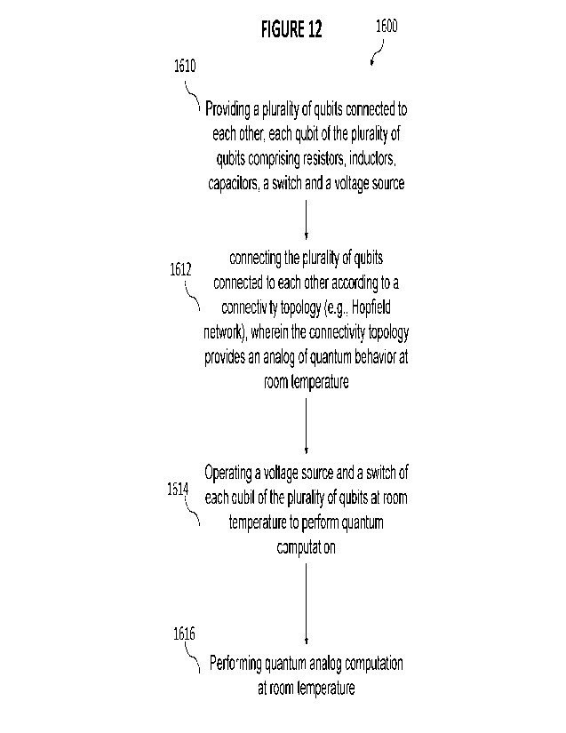
capacitors, a
switch and a voltage source;
[0121]
Step 1612: connecting the plurality of qubits connected to each other
according to a connectivity topology (e.g., Hopfield network), wherein the
connectivity topology provides an analog of quantum behavior at room
temperature;
CA 03180580 2022- 11- 28
WO 2021/237362
PCT/CA2021/050723
32
[0122] Step 1614: operating a voltage source and a switch of
each qubit of
the plurality of qubits at room temperature to perform quantum computation;
and
[0123] Step 1616: performing quantum computation at room
temperature.
Experimental Results
[0124] As a first step, we will approach the problem by
experimental
measurements of the computation structure (qubit). Each analog circuit (or
qubit)
is mathematically equivalent to (or are doppelganger of) an atom in lambda-
configuration.
[0125] More specifically, in an example showing how the
computation
structure may be used to be analog to a real-life system, the analog system
represents the dynamics of an electron in an atom irradiated by two laser
beams
(known as pumping and probe), as shown in Fig. 13C, which couple the two
ground states to their common excited state (where the states 11) and 12) are
the
two ground states while the excited state is represented by 10)). Within this
context,
two possible paths are available. This allows exploiting the superposition
effect to
efficiently explore the space of solution and find the best solution available
in that
space. The functionality of the analog circuit (which is analog to the
behavior of the
system of Fig. 13C, and also based on analog electronics) was experimentally
verified (by setting-up a system as in Fig. 13C) and compared with the
"theoretical"
or simulated results (i.e., simulated with CAD design software) obtained
during the
design phase. The theoretical and experimental results are shown in Figs. 13A-
13B. The left-hand side column depicts the Rabi oscillations (1710, 1720,
1730,
1740) observed during the simulation for different values of the circuit
representing
the pump laser acting on the system of Fig. 13C of which the circuit is an
analog.
The right-hand side column represents the corresponding Fourier transforms
(1712, 1722, 1732, 1742). From the plots, it is easy to observe how the
initial
Gaussian shape splits into two peaks as the circuit corresponding to the pump
laser influence is increased, a typical signature of certain quantum effects.
CA 03180580 2022- 11- 28
WO 2021/237362
PCT/CA2021/050723
33
[0126]
Now referring to Figs. 13A-13B, there is shown a comparison of
measured and simulated Rabi oscillations. The left-hand plots depict the Rabi
frequency measured experimentally (blue) along with simulation results (red).
The
right-hand plots represent the corresponding Fourier transform of the Rabi
oscillations of the experimental (blue) and computational (red) results. It is
evident
that the initial Gaussian shape splits into two peaks as the pump laser
influence is
increased.
[0127]
To showcase the computational capabilities for the quantum analog
device according to an embodiment, two benchmarks were carried out, namely the
Traveling Salesperson Problem and the Black-Scholes model.
[0128]
The first benchmark carried out on the quantum analog device was
the Traveling Salesperson Problem. The problem is part of an important
category
of optimization problems, and it is encountered in various scientific and
engineering areas, moreover it is an NP hard problem, necessitating
exponential
time in order to be solved by brute force method.
[0129]
Fig. 14A depicts the results for up to 100 cities, obtained by the
quantum analog device according to an embodiment. The results pertain to the
computational time to reach a first solution. Note, the initial solution can
represent
a local minimum and thereby one cannot guarantee that the solution is a global
one. The plots show that with the addition of more cities, the quantum analog
device according to an embodiment always remains in the sub-exponential
regime.
A comparison with the Gradient Descent method, shown in Fig. 14B, illustrates
that the gradient descent continues to grow with each city added. The results
for
the gradient descent method have been obtained using Intel(R) Core(TM) i7 -
7500U running at 2.70GHz processor.
[0130]
The second problem involves the ability of the device to tackle partial
differential equations (PDEs), in this case is represented as the Black-
Scholes
equation. The vast majority of PDEs do not have an exact solution and
therefore
CA 03180580 2022- 11- 28
WO 2021/237362
PCT/CA2021/050723
34
necessitate the use of numerical methods such as the finite difference method
(FDM). In the FDM, one discretizes the variable domain and approximates
partial
derivatives by difference quotients based on Taylor's theorem. The resultant
equation represents a system of linear equations which can be solved via
standard
linear algebra libraries or recast as an optimization problem.
[0131]
In the case of the Black-Scholes model, one should note, an exact
solution exists only for the pricing of the European options and cannot be
used in
other cases. At the same time, since the European option model has an exact
analytic solution, it can be used for a comparison of results. To this end,
the Black-
Scholes model has been recast in terms of an optimization problem suitable for
running on the quantum analog device. For comparison purposes, the same
problem has been computed by using Covariance matrix adaptation evolution
strategy (CMA-ES), which is considered a state-of-the-art optimization
algorithm,
developed by N. Hansen from the French Institute for Research in Computer
Science and Automation. Evolution strategies (ES) are stochastic, derivative-
free
methods for numerical optimization of non-linear or non-convex continuous
optimization problems.
[0132]
The accuracy of the quantum analog device has been validated for
those 4 cases: for 10, 50, 100, and 200 number of asset points per time step
(each
computation contains 5 time steps) to obtain timing data as the number of
variables
increase. The accuracy of the quantum analog devices is compared with results
obtained with CMAES, as well as a classical implicit method for the European
Call,
as shown in Fig. 16. In Fig. 16, the accuracy of the quantum analog results is
compared to CMAES results and implicit method for the Black Scholes model for
(upper left plot), 50(upper right plot), 100 (lower left plot), and 200 (lower
right
plot) price points. The plots simply show that the point results match the
curves.
[0133]
The classical stochastic optimization was carried out on 2 GHz
Quad-Core Intel Core i5 device. Table 1 shows the computational performance of
the quantum analog device according to an embodiment, against the classical
CA 03180580 2022- 11- 28
WO 2021/237362
PCT/CA2021/050723
stochastic optimization method (CMAES) implemented on a classical computer
processor, which can be also shown in Fig. 15. The results indicate a
significant
gain of time of computation, as the time of computation does not grow
exponentially with the quantum analog device according to an embodiment, as it
is the case when using classical methods.
Asset price points Quantum Analog Device Classical
stochastic
(CMAES) - Intel
10 0.027454 0.05491
50 0.105662 9.987797
100 0.478005 176.996106
200 41.470628 5862.148043
[0134]
Table 1: Black-Scholes timing comparison between the quantum
analog device and the classical CMAES method for 10, 50, 100, and 200 asset
variables (time is in seconds), as also shown in Fig. 15.
Scalability
[0135]
The quantum analog method as described herein does not suffer
from scalability issues, since the qubits and connections are built from
traditional
CMOS type equipment. This ensures the quality of the qubits, making them
virtually identical due to the CMOS technology implementation. CMOS
scalability
and connectivity are ensured since the technology is very well known and
understood for decades. Maintenance problems are also well known and
relatively
cheap to carry out. Most importantly, additional qubits can be added to the
system
provided the connectivity is precisely calculated, meaning the connectivity
can be
easily reconfigured. Moreover, as seen in the Hopfield based hardware neural
network, we can build application-specific architectures based on classical
circuitry
(ASIC-like capabilities).
7. Conclusions
CA 03180580 2022- 11- 28
WO 2021/237362
PCT/CA2021/050723
36
[0136] In summary, an analog computational structure (qubit)
can be
formed by coupled circuits comprised of resistors, inductors, capacitors and a
switch, powered by a voltage source or their equivalent. It can be embodied on
a
CMOS integrated circuit. A plurality of these CMOS qubits that express the
quantum nature of two-level (or N-level) atomic systems can be connected
together according to a connectivity topology on an integrated circuit in
particular
ways. The CMOS Qubits advantageously work at room temperature. It means that
typical disadvantages normally associated with cryogenic technology in the
context of quantum computing are completely avoided while performing quantum
computing.
[0137] As mentioned above, the architecture of neural networks
can be
used as a way to connect a plurality of qubits together according to such an
architecture. Advantageously, the architecture of the neural network can be
chosen to have a network in which a minimum of energy (stable state) can be
reached through the quantum analog computer in which the qubits are connected
according to such a network. Without limitation, an example of such a network
architecture is the Hopfield network. When the qubits are connected in such a
network, they can reach a stable state during operation. This can be used to
perform quantum analog computing, such as quantum annealing.
[0138] In such a connectivity network, all qubits participate
in the
computation. Scalability and low maintenance are other benefits of this
technology.
[0139] While preferred embodiments have been described above
and
illustrated in the accompanying drawings, it will be evident to those skilled
in the
art that modifications may be made without departing from this disclosure.
Such
modifications are considered as possible variants comprised in the scope of
the
disclosure.
[0140] References, incorporated herein by reference, are as
follows:
CA 03180580 2022- 11- 28
WO 2021/237362
PCT/CA2021/050723
37
[1] R. Feynman, Simulating physics with computers. International Journal of
Theoretical Physics 21, 6&7, 467488, 1982.
[2] Y. Manin. Computable and Uncomputable; Sovetskoye Radio: Moscow, 1980.
[3] John. A. Pople. Nobel lecture: Quantum chemical models. Reviews of Modern
Physics 71.5 (1999): 1267.
[4] W. Kohn. Nobel Lecture: Electronic structure of matterwave functions and
density functionals. Reviews of Modern Physics 71.5 (1999): 1253.
[5] D. Deutsch. Quantum theory, the ChurchTuring Principle and the universal
quantum computer. Proceedings of the Royal Society A, 400(1818), 97, (1985).
[6] Gambetta JM, Chow JM, Ste_en M. Building logical qubits in a
superconducting
quantum computing system. npj Quantum Information. 2017, Jan 13:3(1):1-7.
[7] Corcoles, Antonio D., et al. "Demonstration of a quantum error detection
code
using a square lattice of four superconducting qubits." Nature communications
6.1
(2015): 1-10.
[8] Neill, Charles, et al. "A blueprint for demonstrating quantum supremacy
with
superconducting qubits." Science 360.6385 (2018): 195-199.
[9] Krantz, Philip, et al. "A quantum engineer's guide to superconducting
qubits."
Applied Physics Reviews 6.2 (2019): 021318.
[10] Harty, T. P., et al. "High-fidelity preparation, gates, memory, and read
out of a
trapped-ion quantum bit." Physical review letters 113.22 (2014): 220501.
[11] Schaefer, V. M., et al. "Fast quantum logic gates with trapped-ion
qubits."
Nature 555.7694 (2018): 75-78.
[12] Christopher J. Ballance. Trapped-Ion Qubits. High-Fidelity Quantum Logic
in
Ca+. Springer, Cham, 2017. 5-14.
[13] Zwanenburg, Floris A., et al. "Silicon quantum electronics." Reviews of
modern
physics 85.3 (2013): 961.
CA 03180580 2022- 11- 28
WO 2021/237362
PCT/CA2021/050723
38
[14] Bradley, C. E., et al. "A ten-qubit solid-state spin register with
quantum
memory up to one minute." Physical Review X 9.3 (2019): 031045.
[15] Gumann, P., et al. "Inductive measurement of optically hyperpolarized
phosphorous donor nuclei in an isotopically enriched silicon-28 crystal."
Physical
review letters 113.26 (2014): 267604.
[16] Lester, Brian, et al. "Individual control of an array of neutral atom
qubits for
quantum computing." Bulletin of the American Physical Society (2020).
[17] Picken, C. J., et al. "Entanglement of neutral-atom qubits with long
ground-
Rydberg coherence times." Quantum Science and Technology 4.1 (2018):
015011.
[18] Farhi E, Goldstone J, Gutmann S, Sipser M. Quantum computation by
adiabatic evolution. arXiv preprint quant-ph/0001106. 2000 Jan 28.
[19] Garrido Alzar, C. L., M. A. G. Martinez, and P. Nussenzveig. "Classical
analog
of electromagnetically induced transparency." American Journal of Physics 70.1
(2002): 37-41.
[20] Z. Bai, C. Hang, G. Huang. Classical analogs of double
electromagnetically
induced transparency. Optics Communications, 291, pp.253-2 258,2013.
[21] PW. Shor. Scheme for reducing decoherence in quantum computer memory.
Phys Rev A. 1995;52: R2493.
[22] Jordan, Stephen P., Edward Farhi, and Peter W. Shor. "Error-correcting
codes
for adiabatic quantum computation." Physical Review A 74.5 (2006): 052322.
[23] N. Chancellor, S. Zohren, P.A. Warburton. Circuit design for multibody
interactions in superconducting quantum annealing systems with applications to
a
scalable architecture. npj Quantum Information, 3(1), pp.1-7.2017.
[24] John, Hopfield. Neural networks and physical systems with emergent
collective computational abilities. Proceedings of the national academy of
sciences
79.8 (1982): 2554-2558.
CA 03180580 2022- 11- 28
WO 2021/237362
PCT/CA2021/050723
39
[25] John, Hopfield. Neurons with graded response have collective
computational
properties like those of two-state neurons. Proceedings of the national
academy
of sciences 81.10 (1984): 3088-3092.
[26] D. Tank, J. J. Hopfield. Simple 'neural optimization networks: An AID
converter, signal decision circuit, and a linear programming circuit. IEEE
transactions on circuits and systems 33.5 (1986): 533-541.
[27] J. Hopfield, D. Tank. Computing with neural circuits: A model. Science
233.4764 (1986): 625-633.
[28] Brecht T, Pfaff W, Wang C, Chu Y, Frunzio L, Devoret MH, Schoelkopf RJ.
Multilayer microwave integrated quantum circuits for scalable quantum
computing.
npj Quantum Information. 2016 Feb 23;2(1):1-4.
[29] D-Wave Documentation. Accessed: 14. April 2020. https:
==docs: dwavesys: corn =docs= latest=cgs4: html
[30] S.J. Weber,G.O. Samach, D. Hover, S. Gustaysson, D.K. Kim, A. Melville,
D.
Rosenberg, A.P. Sears, F. Yan, J.L. Yoder, W.D. Oliver. Coherent coupled
qubits
for quantum annealing. Physical Review Applied, 8(1), p.014004, 2017.
[31] K.L. Pudenz, T. Albash, D.A Lidar. Error-corrected quantum annealing with
hundreds of qubits. Nature communications, 5(1), pp.1-10., 2014.
[32] D. Ferrari, M. Amoretti. Demonstration of envariance and parity learning
on
the IBM16 qubit processor. arXiv preprint arXiv:1801.02363. 2018.
[33] Jiang, Nian-Quan, et al. "Universal quantum computing with
superconducting
charge qubits." arXiv preprint arXiv:1809.01304 (2018).
[34] Mills, Jonathan Wayne, and Charles A Daffinger. "An analog VLSI array
processor for classical and connectionist Al." [1990] Proceedings of the
International Conference on Application Specific Array Processors. IEEE, 1990.
[35] Truitt, Thomas D., and Alan E. Rogers. Basics of analog computers. Vol.
256.
JF Rider, 1960.
CA 03180580 2022- 11- 28
WO 2021/237362
PCT/CA2021/050723
[36] Barrios, G. Alvarado, et al. "Analog simulator of integro-differential
equations
with classical mem ristors." Scientific reports 9.1 (2019): 1-10.
[37] Ambrogio, Stefano, et al. "Equivalent-accuracy accelerated neural-network
training using analogue memory." Nature 558.7708 (2018): 60-67.
[38] Tait, Alexander N., et al. "Neuromorphic photonic networks using silicon
photonic weight banks." Scientific reports 7.1 (2017): 1-10.
[39] Shen, Yichen, et al. "Deep learning with coherent nanophotonic
circuits." Nature Photonics 11.7 (2017): 441.
[40] Lin, Xing, et al. "All-optical machine learning using diffractive deep
neural
networks." Science 361.6406 (2018): 1004-1008.
[41] Tzanakis, Constantinos. "Discovering by analogy: the case of
SchrOdinger's
equation." European journal of physics 19.1 (1998): 69.
[42] Eberly, J. H. Seventh Rochester Conference on Coherence and Quantum
Optics. ROCHESTER UNIV NY DEPT OF PHYSICS AND ASTRONOMY, 1996.
[43] Scully, M. 0. "Zubairy (1997) Quantum optics." (2002).
[44] Herrmann, F., and G. Bruno Schmid. "Analogy between mechanics and
electricity." European Journal of Physics 6.1 (1985): 16.
[45] Sivardiere, J. "On the analogy between inertial and electromagnetic
forces." European Journal of Physics 4.3 (1983): 162.
[46] Charru, Francois. "A simple mechanical system mimicking phase transitions
in a one-dimensional medium." European Journal of Physics 18.6 (1997): 417.
[47] Bliokh, Yury P., et al. "Transport and localization in periodic and
disordered
graphene superlattices." Physical Review B 79.7 (2009): 075123.
[48] Timp, G., et al. "Nanostructure Physics and Fabrication, edited by MA
Reed
and WP Kirk." (1989): 331.
CA 03180580 2022- 11- 28
WO 2021/237362
PCT/CA2021/050723
41
[49] SoIs, Fernando, et al. "On the possibility of transistor action based on
quantum
interference phenomena." Applied physics letters 54.4 (1989): 350-352.
[50] Wang, Y., and S. Y. Chou. "Quantum wave bandstop filters." Applied
physics
letters 65.16 (1994): 2072-2074.
[51] Weisshaar, A., et al. "Analysis of discontinuities in quantum waveguide
structures." Applied physics letters 55.20 (1989): 2114-2116.
[52] Weisshaar, Andreas, et al. "Analysis and modeling of quantum waveguide
structures and devices." Journal of applied physics 70.1 (1991): 355-366.
[53] Gaylord, Thomas K., G. N. Henderson, and Elias N. Glytsis. "Application
of
electromagnetics formalism to quantum-mechanical electron-wave propagation in
semiconductors." JOSA B 10.2 (1993): 333-339.
[54] Gaylord, T. K., and K. F. Brennan. "Electron wave optics in
semiconductors." Journal of applied physics 65.2 (1989): 814-820.
[55] Gaylord, T. K., E. N. Glytsis, and K. F. Brennan. "Electron-wave quarter-
wavelength quantum well impedance transformers between differing energy-gap
semiconductors." Journal of applied physics 67.5 (1990): 2623-2630.
[56] Carati, A., and L. Galgani. "Theory of dynamical systems and the
relations
between classical and quantum mechanics." Foundations of Physics 31.1 (2001):
69-87.
CA 03180580 2022- 11- 28