Note: Descriptions are shown in the official language in which they were submitted.
WO 2022/035575
PCT/US2021/042690
System and Method for Global Synchronization of
Time in a Distributed Processinq Environment
CROSS-REFERENCE TO RELATED APPLICATIONS
[0001] This application claims the benefit of United States
provisional patent application
Serial No. 63/065,011, filed August 13, 2020, the disclosure of which is
hereby incorporated
herein by reference in its entirety.
FIELD OF THE DISCLOSURE
[0002] Aspects of the disclosed subject matter relate generally to
high performance data
processing, and more particularly to a system and method employing a precisely
synchronized
time system in connection with a distributed hardware architecture.
BACKGROUND
[0003] Recently, "Big Data," high performance computing, and solid
state device technologies
have become increasingly important in many contexts, such as in connection
with machine
learning and artificial intelligence projects, for instance. With the
explosion of data available to
such systems (as a result, for example, of the nascent Internet of Things
("loT"), distributed
memory systems, and other processing paradigms involving devices sharing data
with other
devices), the sheer volume of available data to process is increasing faster
than traditional
hardware and software systems are able to evolve in order to process those
data in a meaningful
and efficient manner.
[0004] Further, most conventional systems designed for high
throughput data processing and
analytics rely upon exhaustive (or "brute force") approaches that attempt to
overpower the
magnitude of the challenge with overwhelming computational resources, at the
expense of cycle
time and power consumption. As a practical matter, it will be appreciated that
for as long as the
rate at which new data become available for processing continues to outpace
the rate at which
processing methodologies advance to accommodate the increased size of a given
dataset, it will
continue to take longer to solve bigger and more complex data processing
problems ¨ or solutions
providers will continue to throw more resources at those problems.
[0005] Therefore, there is a need for an improved system and method
employing a precisely
synchronized time in connection with a distributed hardware architecture for
resource-intensive
applications; as set forth below, some implementations of such a precisely
synchronized time may
be configured and operative to leverage external signals received from an
independent trusted
CA 03182217 2022- 12- 9
WO 2022/035575
PCT/US2021/042690
source that may be used as "global" or "universal" time across all compute
nodes or other
processing resources.
SUMMARY OF THE DISCLOSURE
[0006] The following presents a simplified summary of the disclosure
in order to provide a
basic understanding of some aspects of various embodiments disclosed herein.
This summary
is not an extensive overview of the disclosure. It is intended neither to
identify key or critical
elements of the disclosed embodiments nor to delineate the scope of those
embodiments. Its
sole purpose is to present some concepts of the disclosed subject matter in a
simplified form as
a prelude to the more detailed description that is presented later.
[0007] The present disclosure describes a system and method
employing a precisely
synchronized time in connection with a distributed hardware architecture; in
the context of this
description, a discrete component of such a distributed hardware architecture
is generally referred
to as a "compute node," though other terms may be used by those of skill in
the art. In some
implementations, one or more compute nodes may be utilized to manage and to
execute data
processing operations independent of, though communicatively coupled with, a
host compute
system. Using the system and methodologies set forth below, each compute node,
and
optionally, the host compute system as well, may be synchronized precisely.
Those of skill in the
art will appreciate that distributed processing operations may benefit from
precise time across a
multiplicity of processing resources.
[0008] In accordance with one aspect of the disclosed subject
matter, a method of generating
a local event timestamp having a precise time may generally comprise:
identifying a precision
oscillator signal and using the precision oscillator signal to clock a local
real time clock counter
with sufficient range to represent an absolute time; identifying a trusted
time signal and a pulse
per second signal; employing the trusted time signal to load the local real
time clock counter with
the absolute time; employing the pulse per second signal to synchronize a
second transition of
the local real time clock counter and to reset a high resolution counter
running at a local system
clock frequency; and generating a local event timestamp with a resolution of a
local system clock
period using the absolute time and a high resolution local offset responsive
to the employing the
pulse per second signal.
[0009] Methods are disclosed wherein the using the precision
oscillator signal comprises
utilizing a local oscillator to produce a local clock signal at the local
system clock frequency. In
2
CA 03182217 2022- 12- 9
WO 2022/035575
PCT/US2021/042690
some implementations, the identifying a trusted time signal and a pulse per
second signal
comprises identifying a satellite signal; such as a global positioning system
signal.
[0010] Methods are disclosed wherein the identifying a trusted time
signal and a pulse per
second signal comprises utilizing a timing input/output interface to receive a
precision clock signal
comprising the trusted time signal and the pulse per second signal.
[0011] In some implementations, the generating a local event
timestamp comprises modifying
an indication of the absolute time output from the local real time clock
counter by the high
resolution local offset output from the high resolution counter. In some
methods, the generating
a local event timestamp comprises producing timestamp data comprising a 64 bit
value.
[0012] In accordance with another aspect of the disclosed subject
matter, a system utilizing
precise time signals may generally comprise: a timing input/output interface
to receive a time
signal and a pulse per second signal; a local real time clock counter with
sufficient range to
represent an absolute time, wherein the local real time clock counter is
initiated with an absolute
time from the time signal and synchronized with the pulse per second signal;
and a high resolution
counter running at a local system clock frequency, wherein the high resolution
counter is
synchronized with the pulse per second signal; wherein output from the local
real time clock
counter and the high resolution counter are combined to generate a precision
timestamp for local
system events.
[0013] Systems are disclosed further comprising a local oscillator
to produce a local clock
signal at the local system clock frequency; in some such systems, the local
oscillator is an oven
controlled crystal oscillator.
[0014] Additionally, some systems are disclosed wherein the time
signal and the pulse per
second signal are derived from a satellite signal, such as a global
positioning system signal. In
some such systems, the timing input/output interface comprises a wireless
receiver.
[0015] In some systems, the timestamp comprises an indication of the
absolute time output
from the local real time clock counter modified by a precision offset value
output from the high
resolution counter. The timestamp may comprise a 64 bit value.
[0016] In accordance with still another aspect of the disclosed
subject matter, a system
utilizing precise time signals may generally comprise: a timing input/output
interface to receive a
time signal and a pulse per second signal; a local real time clock counter
initiated with an absolute
time from the time signal and synchronized with the pulse per second signal;
and a high resolution
counter synchronized with the pulse per second signal; wherein an indication
of the absolute time
3
CA 03182217 2022- 12- 9
WO 2022/035575
PCT/US2021/042690
output from said local real time clock counter is modified by an offset output
by said high resolution
counter to generate a timestamp for local system events.
[0017] Systems are disclosed further comprising a local oscillator
to produce a local clock
signal at a local system clock frequency. In some systems, the high resolution
counter is clocked
at the local system clock frequency; alternatively, in other implementations,
the high resolution
counter is clocked faster than the local system clock frequency.
[0018] As noted above, the timing input/output interface may
comprise a wireless receiver to
receive a wireless signal comprising the time signal and the pulse per second
signal, and the
timestamp may comprise a 64 bit value.
[0019] The foregoing and other aspects of various disclosed
embodiments will be apparent
through examination of the following detailed description thereof in
conjunction with the
accompanying drawing figures, in which like reference numerals are used to
represent like
components throughout, unless otherwise noted.
DESCRIPTION OF THE DRAWING FIGURES
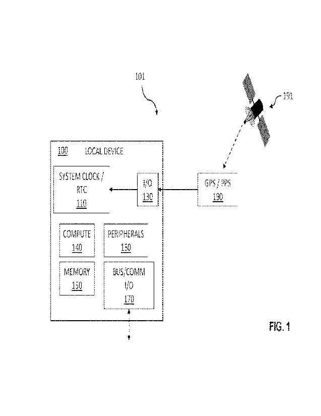
[0020] FIG. 1 is a functional block diagram illustrating one
implementation of a precision time
system for use in connection with a processing resource;
[0021] FIG. 2 is a functional block diagram illustrating one
implementation of a processing
resource using one system for precision time;
[0022] FIG. 3 is a functional block diagram illustrating one
implementation of a system clock
for use in connection with a processing resource; and
[0023] FIG. 4 is a flow diagram illustrating aspects of one
implementation of a method of
generating a local event timestamp having a precise time.
DETAILED DESCRIPTION
[0024] Certain aspects and features of the disclosed subject matter
may be further
understood with reference to the following description and the appended
drawing figures. In
operation, a system and method employing time that is precisely synchronized
across
independent processing resources may have utility in connection with various
data processing
strategies and data analytics implementations. Specifically, the present
disclosure provides for a
distributed data processing platform that may generally comprise hardware and
software, all
operating on precisely synchronized, or "absolute," time.
4
CA 03182217 2022- 12- 9
WO 2022/035575
PCT/US2021/042690
[0025] It will be appreciated by those of skill in the art that a
reliable clock across multiple
(say, eight or more, in some implementations) compute nodes or processing
resources is a
significant technical challenge. Increasingly, processing intensive compute
operations rely upon
very precise timing with small margins for error. For example, a system
designer or operator may
have a need or desire to compare log file data available from each of the
nodes or resources, and
since each is independent (or "self-contained"), the lack of a universal,
absolute, or precisely
synchronized clock can make the order of events difficult to ascertain. In
this context and others,
the disclosed subject matter may provide the same normalized, universal,
global, or absolute time
timestamp, not only across the nodes in a single module or device, but also
across the nodes of
multiple modules in the same server, in the same datacenter, or even across
data centers.
[0026] In the context of this disclosure, the terms "normalized,"
"universal," "global," and
"absolute" time are intended to mean that the clocks for multiple processing
resources are, for all
practical purposes as set forth below, precisely synchronized to a sufficient
degree that a high-
precision local offset is enough to establish (or additionally or
alternatively to govern, control, or
otherwise to regulate) a sequence of events across the multiple processing
resources within a
margin of error that is satisfactory to the system designer. In that sense,
those of skill in the art
will appreciate that the concept of "absolute" time may be application-
specific, depending upon,
for example, the precision of the processing resources and the intricacies of
the processing
operations, local clock frequencies, temperature variations, or a combination
of these and a
variety of other factors.
[0027] In use, a system and method for global synchronization of
time described below may
provide a known absolute time ¨ irrespective of location in the distributed
environment ¨ that is
accessible to hardware and software applications, algorithms, or other
processing operations (for
instance, through an application programming interface (API) or other
mechanism). It will be
appreciated that this absolute time is independent of local server time or
network time skew.
Accordingly, system operators or application programmers may precisely track
when a given
interaction with a processing resource, or a particular processing resource
within a particular
module or other device, took place ¨ read, write, run algorithm, get results,
and/or other system
events may be monitored, or even controlled, in absolute time that is
precisely synchronized
across all hardware and software resources in a distributed processing
architecture.
[0028] Implementation of precisely synchronized time across
distributed processing nodes
has utility in a variety of use cases, such as, but not limited to cyber
intrusion detection involving
seeking and identifying patterns of activity in application-provided datasets
which may exist in
CA 03182217 2022- 12- 9
WO 2022/035575
PCT/US2021/042690
multiple, discrete datacenters, but are time series related. As another
example, it may be
beneficial to synchronize a time series database in applications involving
distributed collection of
data and subsequent distributed processing of the data.
[0029] As set forth in more detail below, the present disclosure
addresses enabling absolute
or universal time across such distributed processing architectures. The
architectural framework
generally contemplates one or multiple compute nodes operating in parallel
(and in series, in
some cases), each of which may be configured as a pipeline of computational
elements that can
be configured and operative to implement a variety of algorithms or other data
processing
operations. In the configurations provided as examples, each processing
resource has a local
real time clock counter that may be influenced by and synchronized to a
trusted external timing
signal received from an independent source.
[0030] Turning now to the drawing figures, FIG. 1 is a functional
block diagram illustrating one
implementation of a precision time system for use in connection with a
processing resource. As
illustrated, one implementation of system 101 may generally comprise a compute
system or
processing resource (Le., local device 100) and a source 190 of a timing
signal.
[0031] Device 100 may generally be embodied in or comprise a
computer server, a desktop
or workstation computer, a laptop or portable computer or tablet, or a
combination of one or more
of such components. In operation, device 100 may be employed to initiate,
instantiate, or
otherwise to effectuate data processing operations as is generally known in
the art. In that regard,
device 100 may include one or more microprocessors, field programmable gate
arrays (FPGAs),
microcontrollers, or other digital processing apparatus (reference numeral
140), along with
attendant memory (reference numeral 150), controllers and firmware (not
illustrated in FIG. 1 for
clarity), network interface hardware (reference numeral 170), and the like.
For example, device
100 may generally comprise multiprocessor systems, microprocessor-based or
programmable
consumer electronics, personal computers ("PCs"), networked PCs,
minicomputers, mainframe
computers, and similar or comparable apparatus for general purpose or
application-specific data
processing. Various implementations of device 100 may be deployed in
distributed computing
environments in accordance with which tasks or program modules may be
performed or executed
by remote processing devices, which may be linked through a communications
network. Those
of skill in the art will appreciate that any of various computer servers, work
stations, or other
processing hardware components or systems of components may be suitable for
implementation
at device 100, and that the disclosed subject matter is not limited to any
particular hardware
implementation or system architecture employed at device 100.
6
CA 03182217 2022- 12- 9
WO 2022/035575
PCT/US2021/042690
[0032] In the FIG. 1 example, device 100 is illustrated as
comprising a compute component
140, memory 150, peripherals 160, and network interface hardware (or
input/output (I/O)
interface) 170. Specifically, with respect to requesting, initiating,
enabling, facilitating, and
receiving results of any data processing operations, device 100 may be
communicatively coupled
to routers, bridges, communications channels, or other networked devices, such
as via a bus or
communications hardware represented by I/O interface 170. In operation, I/O
interface 170
generally enables bi-directional data transmission in accordance with any of
various
communications interfaces or telecommunications protocols generally known in
the art or
developed and operative in accordance with known principles, and generally
supports the use of
device 100 in a distributing processing architecture.
[0033] Compute component 140 may generally comprise one or more
microprocessors,
FPGAs, application specific integrated circuits (ASICs), programmable logic
blocks,
microcontrollers, or other digital processing apparatus suitable for data
processing in accordance
with requirements or design specifications of device 100. Typically, compute
component 140
cooperates with or operates in connection with memory 150, which may generally
comprise or
have access to, by way of example, volatile memory such as random access
memory (RAM) in
any of its various forms, for instance, static RAM (SRAM), dynamic RAM (DRAM),
double-data
rate (DDR) RAM, and the like; in some applications, DDR4 RAM may be used as or
in connection
with memory 150. Additionally or alternatively, memory 150 may be embodied in
or generally
comprise a mass data storage component, such as a non-volatile data storage
device, one
example of which is an Electronically Erasable Programmable Read Only Memory
(EEPROM)
store. For example, memory 150 may be, or include, Flash memory, though other
memory types
having suitable or appropriate characteristics to facilitate the functionality
of device 100 may be
in use currently or developed in the future. Specifically, any of various
types of processing
hardware and firmware, as well as volatile and non-volatile storage media, may
have utility in the
context of operation of device 100 (which may be application- or system-
specific), and the present
disclosure is not intended to be limited by the nature or operational
characteristics of memory 150
or of compute component 140.
[0034] Similarly, device 100 may include or have access to
functional characteristics of any
of a number of peripherals 160, such as hardware or firmware modules, external
components,
and the like, that generally support or enable operation of compute component
140 in cooperation
with memory 150. Typical peripherals 160 include monitors or displays,
keyboards, trackpads, or
other input devices, external memory stores such as disk drives or removable
storage media, or
7
CA 03182217 2022- 12- 9
WO 2022/035575
PCT/US2021/042690
other components as are generally known in the art. Peripherals 160 are
typically connected via
bus structures or I/O hardware, which are not illustrated in FIG. 1 for
clarity. Those of skill in the
art will appreciate that the present disclosure contemplates any of myriad
peripherals 160 that
support or enable operation of compute component 140 in the context of desired
or required
operation of device 100.
[0035] Device 100 also comprises a system clock 110, which generally
governs timing of
events executing at device 100, as well as timing for operation of the
constituent components of
device 100 (as best illustrated in FIG. 2 and addressed in more detail below).
[0036] As illustrated in FIG. 1, device also includes a timing I/O
interface 130. In operation,
timing I/O interface 130 may generally receive a signal from source 190 and
subsequently
communicate that signal (either directly or indirectly via appropriate
signaling hardware) to system
clock 110. In some implementations, timing I/O interface 130 may be embodied
in or comprise
suitable wireless hardware to receive a signal from source 190 wirelessly; in
these instances, any
of various wireless communications protocols and hardware infrastructure may
be utilized. For
example, timing I/O interface 130 may be configured and operative in
accordance with wireless
local area network (LAN) technologies such as the 802 standard promulgated by
the Institute of
Electrical and Electronics Engineers (IEEE), e.g., IEEE 802.11 or Ethernet,
IEEE 802.3.
Additionally or alternatively, timing I/O interface 130 may include a physical
or structural connector
or connection mechanism, such as a network interface card, hardware component,
or
communications port, jack, or plug, such as are generally known in the art or
to be developed in
accordance with known principles. It will be appreciated that the
implementation of timing I/O
interface 130 may depend upon the hardware or operational characteristics of
source 190 and
the manner in which source 190 provides the timing signal (e.g., wirelessly or
wired).
[0037] In operation, source 190 provides an independent (i.e.,
external to, and not dependent
upon operation of, device 100) trusted timing signal to timing I/O interface
130. Source 190 may
be implemented as or generally comprise a source for global positioning system
(GPS) timing
signals, such as those received from a GPS satellite 191. It is noted that
FIG. 1 is stylized, and
that additional satellites are omitted for clarity. In some implementations,
for instance, where
timing I/O interface 130 comprises suitable receiver functionality, timing I/O
interface 130 may
receive timing signals directly from satellite 191, or from multiple such
satellites as is generally
known in the satellite positioning or navigation art. In other
implementations, satellite 191, or a
combination of such satellites, may transmit timing signals to an intermediary
system or hardware
structure, which then may relay such timing signals to timing I/O interface
130. In FIG. 1, source
8
CA 03182217 2022- 12- 9
WO 2022/035575
PCT/US2021/042690
190 is intended to depict both of the foregoing embodiments, and generally to
represent a trusted
source of an independent timing signal. In the illustration, that signal is a
GPS signal, but other
timing signals are also contemplated, such as from other global navigation
satellite systems
(GNSSs) such as Russia's Global Navigation Satellite System (GLONASS), China's
BeiDou
Navigation Satellite System (BDS), and Europe's Galileo system. Those of skill
in the art will
appreciate that satellite technology is not necessary for suitable
implementation of source 190,
and that other universal or precision clocks (such as the one maintained by
the National Institute
of Standards and Technology (N 1ST)) may be used for source 190 in some
applications.
[0038] FIG. 2 is a functional block diagram illustrating one
implementation of a processing
resource using a system for precision time. In that regard, FIG. 2 is a more
detailed view of the
device 100 illustrated in FIG. 1, showing a local system clock signal, CLKo,
distributed by system
clock 110. As noted above, system clock 110 generally governs timing for
operation of all of the
constituent components of device 100.
[0039] Of interest in FIG. 2 is that compute component 140 and
memory 150 are illustrated
as having multiple sub-components. For instance, compute component 140 may
comprise a
plurality of processing sub-components such as microprocessors PROC.1,
PROC.2,
PROC.,,, each of which may be embodied in or comprise one or more of the
processing hardware
technologies set forth above. Similarly, memory 150 may comprise a plurality
of memory stores
such as Memoryl, Memory2, Memory, each of which may be embodied in one or more
of the
memory types discussed above and may generally be operative to store data and
instructions
necessary or desirable for compute component 140 to perform write/read/execute
operations in
support of device 100 functionality as is generally known. Busses,
communication pathways,
controllers and other supporting hardware, etc. have been omitted from FIG. 2
for clarity.
[0040] As illustrated in FIG. 2, and as is generally known in the
art, system clock 110 may
distribute CLK0 to peripherals 160, I/O interface 170, compute component 140
(and its constituent
sub-components), and memory 150 (and its constituent sub-components). In a
departure from
conventional hardware architectures, however, system clock 110 may be informed
by an external
timing signal provided by source 190, such as via timing I/O interface 130, as
set forth in more
detail below.
[0041] In that regard, FIG. 3 is a functional block diagram
illustrating one implementation of a
system clock for use in connection with a processing resource. In the FIG. 3
example, system
clock 110 is illustrated as generally comprising a real time clock counter
(RTC 112), a high-
resolution counter 113, and a local oscillator 111 that serves as a source for
CLKo. As is typical
9
CA 03182217 2022- 12- 9
WO 2022/035575
PCT/US2021/042690
in many applications, local oscillator 111 may be embodied in or generally
comprise a precision
oscillator suitable for high-speed data processing applications or otherwise
for the design
specifications of device 100; an oven controlled crystal oscillator (OCX0) is
one example, though
the present disclosure is not intended to be limited by the nature or the
operational characteristics
of the oscillator used by or in local oscillator 111. In operation, local
oscillator 111, irrespective of
its type or specific implementation, may be utilized to produce and to
distribute a clocking signal
at a predetermined or a selectively controlled frequency ¨ for example, the
frequency output by a
typical OCXO may be temperature-dependent, and so precise control of
temperature may allow
for fine adjustments in frequency of CLKo output from local oscillator 111.
[0042] In some implementations, counter 113 may be configured and
operative to run at
CLKo, as illustrated, but other clock frequencies, typically higher than CLKo,
may be appropriate
for some applications. In operation, counter 113 may be used to provide high-
resolution clock
timing, at CLKo, for example, synchronized each second with the trusted
external clock signal
from source 190 substantially as set forth below. Any of numerous counter
hardware components
or technologies generally known in the art may be suitable for implementation
as counter 113.
[0043] In the FIG. 3 example, timing I/O interface 130 may receive
both a GPS signal and a
pulse per second (PPS) signal (e.g., from source 190), and may subsequently
supply those
signals to system clock 110. Specifically, a PPS signal may be provided (i.e.,
at a frequency of
1Hz) to counter 113 such that counter 113 may be reset at regular 1 second
intervals in
synchronization with the signal provided by source 190 via timing I/O
interface 130. Similarly, a
PPS signal may also be provided to RTC 112 such that a second counter at RTC
112 may be
advanced in synchronicity with the signal provided by source 190 via timing
I/O interface 130; this
feature allows RTC 112 to maintain local time consistent with the trusted
timing signal provided
by source 190. Specifically, RTC 112 may set local time according to the GPS
signal, and the
PPS signal may be used to ensure that the second transitions in RTC 112 occur
precisely at the
second transitions of the GPS signal.
[0044] In summary, RTC 112 may set local time as a function of a GPS
signal, and may
periodically synchronize an output RTC signal using pulses in the PPS signal;
counter 113 may
similarly be synchronized to the pulses in the PPS signal such that an offset
between CLK0 and
the PPS signal may be determined. RTC 112 may then output an RTC signal (for
example, a 32-
bit output signal) representative of real time, and counter 113 may output an
offset signal (for
example, a 32-bit output signal), both of which may be employed to create a
timestamp for a given
system event occurring in device 100. Those of skill in the art will
appreciate that the RTC and
CA 03182217 2022- 12- 9
WO 2022/035575
PCT/US2021/042690
offset signals may comprise more or fewer than 32 bits, and that the nature
and bandwidth of
these signals may be application-specific or otherwise dependent upon the
operational
specifications or requirements of device 100 or of the distributed system of
which it is a part.
[0045] As noted above with reference to FIG. 1, other types of
trusted, independent timing
signals (La, other than GPS) may be used for driving the synchronization
illustrated in FIG. 3.
Any signal with a trusted time and an accurate second transition pulse may be
used with similar
effect.
[0046] FIG. 4 is a flow diagram illustrating aspects of one
implementation of a method of
generating a local event timestamp having a precise time. At block 1001, the
method may begin
by identifying a precision oscillator signal; in some implementations, this
signal may be identified
from local oscillator 111 in FIG. 3, for instance, though other embodiments
are contemplated. For
example, the oscillator signal may be embedded in the trusted, independent
timing signal received
from source 190 via timing I/O interface 130, or via another mechanism. As
indicated at block
1002, the precision oscillator signal may be used to clock a local real time
clock counter with
sufficient range to represent an absolute or global time. As set forth above,
the GPS signal (or
other signal from source 190) may provide a numeric value or other timing
indicum to initiate RTC
112 in FIG. 3. In that regard, at block 1003, the method may continue by
identifying a trusted
time signal and a pulse per second signal; as noted above, one example of this
functionality
includes receipt of a GPS signal and a PPS signal from source 190. It is noted
that blocks 1002
and 1003 may be combined or executed substantially concomitantly, depending
upon the nature
of the signal received from source 190 and the manner in which the real time
clock counter is
initiated. For example, if the precision oscillator signal in blocks 1001 and
1002 is embedded in
the trusted time signal, then the operation at block 1002 may be completed by
identifying the
trusted time signal in block 1003. In the example of FIG. 4, the process may
not proceed to block
1003 until a determination is made at decision block 1099 that the local real
time clock counter
(e.g., RTC 112) has been initiated, though this determination may be
incorporated into the
operations at blocks 1002, 1003, or both in some applications. Those of skill
in the art will
appreciate that other alternatives exist that are within the scope and
contemplation of the present
disclosure.
[0047] As indicated at block 1004 the trusted time signal may be
employed to load a local real
time clock counter with absolute time; an example of this is illustrated at
the top of FIG. 3, in which
the GPS time signal is input to the Set Time block in RTC 112, though times
other than GPS time
may also be used. As indicated at blocks 1005 and 1006, the method may proceed
by employing
11
CA 03182217 2022- 12- 9
WO 2022/035575
PCT/US2021/042690
the pulse per second signal to synchronize a second transition of the local
real time clock counter
(e.g., RTC 112) and to reset a high resolution counter running (e.g., counter
113) at a local system
clock frequency (i.e., CLK0); examples of these operations are illustrated in
the middle of FIG. 3.
It is noted that the operations illustrated in blocks 1005 and 1006 may be
reversed in order or
combined without any practical effect. The order of these operations is
presented only for
visualization purposes; in practice, these operations are happening
simultaneously, as both are
occurring in synchronicity with the PPS signal in FIG. 3. Those of skill in
the art will appreciate
that the foregoing subject matter is susceptible of various design choices
that may influence the
order or arrangement of some or most of the operations depicted in FIG. 4.
[0048] Finally, at block 1007, the method may conclude by generating
a local event timestamp
with a resolution of a local system clock period using the absolute time
(e.g., output from RTC
112) and a high resolution local offset generated (e.g., by counter 113)
responsive to the pulse
per second signal.
[0049] In summary, the method makes use of a trusted, independent
time signal and a trusted
PPS signal. In operation, the time signal may provide a numeric value to
initiate and/or to set
absolute time in RTC 112, and the PPS may be used to increment the second
count in RTC 112,
and also to reset high-speed counter 113 that provides a precision offset
since the last second
increment. Output from RTC 112 combined with an offset value output from
counter 113 may be
used as "timestamp data," which may be employed either independently or in
conjunction with
other system data to create a precision (e.g., 64 bit) timestamp for local
system events.
[0050] Several features and aspects of a system and method have been
illustrated and
described in detail with reference to particular embodiments by way of example
only, and not by
way of limitation. Those of skill in the art will appreciate that alternative
implementations and
various modifications to the disclosed subject matter are within the scope and
contemplation of
the present disclosure. Therefore, it is intended that the present disclosure
be considered as
limited only by the scope of the appended claims.
12
CA 03182217 2022- 12- 9