Note: Descriptions are shown in the official language in which they were submitted.
WO 2021/255332
PCT/F12021/050428
1
Manufacturing method of optical element, optical element and
apparatus for manufacturing optical element
Field
The invention relates to a manufacturing method of an optical element,
the optical element and an apparatus for manufacturing it the optical element.
Background
An optical combiner of an augmented reality (AR) eyewear based on a
diffractive grating is often fabricated with a high refractive index films
that are
deposited on top of a transparent substrate serving as a lightguide, and
patterned
in order to form a diffractive optical element (DOE).
The operation of the eyewear implies that light of a visible range is
coupled into a waveguide through a diffractive grating and, after the light
being
distributed inside the waveguide, it is out-coupled through another
diffractive
grating such that a user sees a digital image in addition to surrounding
environment that can be seen through the waveguide. In order to achieve better
image quality, scattering strength of the diffractive grating arrangement
often
should be modulated in a controllable fashion between low and high values with
large differences in scattering intensity across the diffractive grating
arrangement,
e.g. by a factor of 2 to 10 or more.
There are standard ways to modulate scattering strength across the
diffractive grating arrangement including either a variation in grating
pattern itself
or a change in height of grating features (i.e. grating ridge height or
grating groove
depth). The variations of grating pattern are inherently limited by utilized
fabrication processes and often they cannot provide strong enough modulation
in
scattering intensity across the diffractive grating arrangement (e.g. by a
factor of
10 or more). Consequently, in many cases there is a need for controllable
variation
in height of the grating features. However, this type of modulation makes the
fabrication of diffractive grating arrangements more complex and requires the
use
of additional process steps such as: deposition of additional layers,
introduction of
multiple etching steps, use of grayscale lithography, etc. Also, in such
complex
CA 03182746 2022- 12- 14
WO 2021/255332
PCT/F12021/050428
2
fabrication sequences, process yield suffers and fabrication costs increase.
Hence,
there is a fundamental necessity for improvement.
Brief description
The present invention seeks to provide an improvement in
manufacturability of the AR eyewear.
The invention is defined by the independent claims. Embodiments are
defined in the dependent claims.
List of drawings
Example embodiments of the present invention are described below, by
way of example only, with reference to the accompanying drawings, in which
Figures 1A and 1B illustrate examples of an AR eyewear;
Figure 2 illustrates an example of a deposition process;
Figure 3A illustrates an example of a plate with perforations;
Figure 3B illustrates an example of a layer of solid material deposited
onto a waveguide through the plate having perforations;
Figure 3C illustrates an example of a patterned resist or etching mask
on the layer;
Figure 4 illustrates an example of a distribution of heights of ridges of a
diffraction grating, ridges being made of the solid material on a waveguide;
Figure 5A illustrates an example of distributions of heights of ridges
made of a solid material and a cross-sectional areas of perforations of a
plate;
Figure 5B illustrates another example of distributions of heights of the
ridges and the cross-sectional areas of perforations of a plate;
Figure 6 illustrates an example of a curvy plate;
Figure 7 illustrates an example of a DOE which comprises a waveguide
with diffraction gratings; and
Figure 8 illustrates of an example of a flow chart of a manufacturing
method.
CA 03182746 2022- 12- 14
WO 2021/255332
PCT/F12021/050428
3
Description of embodiments
The following embodiments are only examples. Although the
specification may refer to "an" embodiment in several locations, this does not
necessarily mean that each such a reference is to the same embodiment(s), or
that
the feature only applies to a single embodiment. Single features of different
embodiments may also be combined to provide other embodiments. Furthermore,
words "comprising" and "including" should be understood as not limiting the
described embodiments to consist of only those features that have been
mentioned
and such embodiments may also contain features/structures that have not been
specifically mentioned. All combinations of the embodiments are considered
possible if their combination does not lead to structural or logical
contradiction.
It should be noted that while Figures illustrate various embodiments,
they are simplified diagrams that only show some structures and/or functional
entities. The connections shown in the Figures may refer to logical or
physical
connections. It is apparent to a person skilled in the art that the described
apparatus may also comprise other functions and structures than those
described
in Figures and text. It should be appreciated that details of some functions,
structures, and the signalling used for operation are irrelevant to the actual
invention. Therefore, they need not be discussed in more detail here.
Below, a technique to control a local thickness of features of diffraction
grating(s) made of a solid material, which has a high refractive index, is
presented.
The features, which are periodical, may include ridges and grooves of the
diffraction grating(s), for example, an groove locating between any two
directly
adjacent ridges and vice versa. The thickness can be controlled in one or two
dimensions. A fundamental benefit of such an approach is that a thickness
profile
of the features of the solid material with a high refractive index can be
custom-
shaped. The formed profiles are then used for the fabrication of DOE with
scattering efficiency modulation following the deposited film thickness
profiles.
The DOEs can be then formed with only one etching step, for example, unlike in
approaches with multiple etching steps.
CA 03182746 2022- 12- 14
WO 2021/255332
PCT/F12021/050428
4
Figures 1A and 1B illustrate examples of an AR (Augmented Reality)
eyewear. The eyewear may look like glasses, spectacles or goggles, for
example. In
an embodiment, the eyewear may be in connection with a headwear like a cap, a
hat or a helmet, for example. In Figure 1A, the eyewear comprises an optical
element 10 and an image generating unit 12, which in turn may have an image
source 14 and an optic component arrangement 16. The image generating unit 12
generates visible light of an image (still or video) that is coupled to a
waveguide
106 of visible light through the optic component arrangement 16 and a
diffractive
grating 102, which is on a surface of the waveguide 106. In Figure 1B, the eye
wear
comprises two parts A and B, each for one eye 150, 152. The image generating
unit
12 may direct the visible light of the image to the optic component
arrangement
16, which may split the light for the two parts A and B. Instead of optical
splitting,
the eyewear may have two image generating units 12, each for one part A and B.
The waveguide 106 allows visible light to propagate via total internal
reflection from an in-coupling area, where the visible light is in-coupled by
a
diffractive grating 102 into the waveguide 106, to one or more desired areas,
which
have a first out-coupling diffractive element 100 and a second out-coupling
diffractive grating 104. The waveguide 106 may be made up of a transparent
material like glass, sapphire and/or a polymer, for example. The glass may
comprise a high refractive index flint glass family, for example. The
waveguide 106
may also be called lightguide. A refractive index of the waveguide 106 may be
from
about 1.7 to 2 or higher.
The visible light is thus guided laterally within the waveguide 106, and
one or two of the first and second out-coupling diffractive gratings 100, 104
couple
the visible light out of the waveguide 106 in order direct the visible light
into one
or two eyes 150, 152 of a user for showing the image. The out-coupling
diffractive
gratings 100, 104 are used as optical combiners in the AR eyewear. The user
may
namely see the environment through the optical component 10 and the image
scattered from the first and second diffractive gratings 100, 104.
In an embodiment, a distance DD between a first out-coupling
diffractive grating 100 and a second out-coupling diffractive grating 104 may
be at
CA 03182746 2022- 12- 14
WO 2021/255332
PCT/F12021/050428
least approximately the same as a distance DE between eyes 150, 152 of a human
being that is referred to as an interpupillary distance (IPD). The distance DD
may
be about 63 mm, for example. However, the first out-coupling diffractive
grating
100, the in-coupling diffractive grating 102 and the second out-coupling
diffractive
5 grating 104 may form a continuous diffractive element structure on the
waveguide
106 in another embodiment.
As a further detail, the distance DD may be the same as an average or an
estimate of the IPD, for example. The IPD i.e. the distance DE may be about 64
mm
for a male and 62 mm for female, for example. Hence, the distance DD may be
determined as a spacing between a center of the first out-coupling diffractive
grating 100 and a center of the second out-coupling diffractive grating 104.
In an embodiment an example of which is illustrated in Figure 1A, the
eyewear has one optical component 10 and one image generating unit 12 for both
eyes 150, 152.
In an embodiment, the eyewear may have one optical component 10
and one image generating unit 12 per one eye 150, 152.
The diffractive gratings 100 to 104 may be on either side of the
waveguide 106 in an embodiment. In an embodiment, at least one of the
diffractive
gratings 100 to 104 may be on a side of the waveguide 106 opposite to at least
one
other of them.
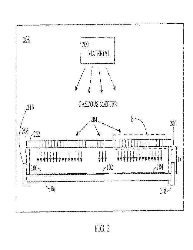
Figure 2 illustrates an example of a deposition process. Material 200
used to form at least one diffractive grating 100, 102, 104 is deposited onto
the
waveguide 106 or a preform of the waveguide 106 through perforations 204 of a
plate 202. During a manufacturing process, the term "waveguide" is also
considered to include the preform of the waveguide 106. The plate 202 is at a
non-
zero distance D from the waveguide 106. The distance D may be set using a
spacer
structure 206, for example. The plate 202 may be supported by the spacer
structure
206. If a shape of the waveguide 106 is a circle, the spacer structure 206 may
be a
ring that is around an outer contour of the waveguide 106. A total thickness
of the
structure including the spacer structure 206 may have a thickness larger than
the
distance D. The spacer structure 206 may have a shape with a circular outer
CA 03182746 2022- 12- 14
WO 2021/255332
PCT/F12021/050428
6
circumference and an inner side with a circular opening, rectangular
opening(s)
and/or other custom-shaped openings that support positioning of the plate
above
the waveguide 106 and screen other areas from getting material 200 deposited
thereon. Hence, the spacer structure 206 may have a thickness equal to the
distance
D. A material of the spacer structure 206 may comprise metal, glass, ceramic
or the
like for example. In an embodiment, the spacer structure 206 may comprise
anodized aluminum, for example.
In an embodiment, the spacer structure 206 may comprise at least one
adjustment arrangement 210. The adjustment arrangement 210 may be
mechanical, electro-mechanical, hydraulic and/or pneumatic, for example. A
mechanical adjustment arrangement may comprise a screw, for example. An
electro-mechanical adjustment arrangement may comprise an electric motor and
a screw that is rotated by the electric motor, for example.
The distance D is an important parameter that may be taken into
account depending on the following: a) type of deposition reactor, nature and
parameters of deposition process; b) thickness of the plate 202; c) feature
size
including height and/or width of the perforations 204 and structure of the
perforations 204 in the plate 202; d) particular DOE layout; e) arrangement of
DOEs on a wafer. Here the DOE layout means that different grating shapes are
possible and depending on the particular shape (e.g., rectangular, bowtie,
triangle,
etc.) the perforations 204 in the plate 202 would have different arrangement.
Arrangement of the DOEs implies that there are different options depending on
how e.g. several DOE with varying heights are positioned with respect to each
other
in order to adjust or control the height profile of the layer 300.
The distance D between the plate 202 and the waveguide 106 may be
set to a specific optimal value. In an embodiment, the distance D may be about
Smm, for example. If the distance D is too small, features of the perforations
204
may not even out sufficiently and the structure of a layer 300 may fail to be
conformal enough. If the distance D is too long, an accuracy of a local film
thickness
control may degrade. In an embodiment, the plate 202 may be tilted with
respect
to the waveguide 106.
CA 03182746 2022- 12- 14
WO 2021/255332
PCT/F12021/050428
7
In an embodiment, the spacer structure 206 may also include additional
elements that are case-specific and are not shown in the drawings. These
elements
may be: a) additional features supporting a shadow mask, b) additional
features
used to screen the areas of fabricated DOE (or around DOE) where high
refractive
materials should not be deposited, i.e. the areas that should stay clean from
the
deposited high refractive index layer.
The material of the plate 202 may comprise metal, glass, ceramic or the
like, for example. In an embodiment, the metal may be stainless steel that may
be
of a high purity, for example. In an embodiment, a thickness of the plate 202
may
between about 0.001 mm to about 1 mm, for example. In an embodiment, a typical
thickness may be about 0.01 mm to about 0.1 mm, for example. In an example,
the
thickness may be about 0.05mm.
In an embodiment, a diameter of the waveguide 106 and the plate 202
may vary from tens of millimeters to 450 mm, for example. A large waveguide
106
may be cut into pieces that are suitable for the eyewear. In an embodiment, a
diameter of the waveguide 106 and the plate 202 may be about 100mm, for
example. The deposition system 208 may be scaled/modified or scalable for
waveguides 106 of smaller/larger diameter.
As shown in an example of Figure 3A, which shows a section E of Figure
2, a cross sectional area of the perforations 204 vary in a determined manner
depending on a location in the plate 202 (only a few of the perforations have
reference number in Figure 3A because all the perforations cannot be marked
with
numbers). In the example of Figure 3A, the cross sectional area of the
perforations
204 varies in the direction of X-axis but keeps constant in the direction of Y-
axis.
In an embodiment, the variation of the cross sectional areas of the
perforations 204 may be one dimensional over a surface of the plate 202 while
the
cross sectional areas of the perforations 204 may remain constant in another
dimension (the perforations can be distributed spatially only in two
dimensions).
The dimensions, each of which can be considered a spatial extent orthogonal to
and/or independent from another dimension, may be those of a Cartesian
coordinate system or a polar coordinate system. In an embodiment, the cross
CA 03182746 2022- 12- 14
WO 2021/255332
PCT/F12021/050428
8
sectional areas of the perforations 204 may vary as a function of values of
both
dimensions.
Figure 3A shows hexagon-type perforation as an example, and
modulation of mask opening areas in the X-direction. Shapes of the
perforations
204 maybe: hexagonal, circular, rectangular, linear, star, any combination of
these,
for example. The shapes of the perforations 204 may also be custom-made.
The plate 202 with the perforations 204 can be made to fulfil a desired
opening-to-solid area ratio or a grating fill factor in the x-direction, the x-
and y-
directions, or custom patterns across the plate 202.
In an embodiment, the solid material 200 may be turned into a flowable
state, which may be a gaseous state or a vapor state, in order to allow its
passing
through the perforations 204 of the plate 202. Then the material 200 in the
flowable state solidifies on the waveguide 106.
In an embodiment, the material transfer for deposition onto a
waveguide may be performed in a vaporized state, for example. Then the solid
material 200 may be turned into a vapor state and the vapor is condensed as
layered or film structure on the waveguide 106 in a vapor deposition process,
for
example. The vapor deposition may be realized using sputtering, chemical vapor
deposition or physical vapor deposition, for example, without limiting to
these.
A person skilled in the art is familiar with various deposition systems
and processes that can be used as the deposition system 208.The solid material
200 may have a refractive index equal to or higher than that of the waveguide
106
in the visible range of light, for example. The refractive index of the
material 200
may in some cases be also lower than that of the waveguide 106. A refractive
index
of the solid material 200 may be in a range about 1.8 to about 2.7 or even
upto 3.5,
for example. However, it may also be lower than about 1.8. A high refraction
index
results in an effective scattering of light, and typically better DOE
performance over
a wide range of in-coupling and out-coupling angles which in turn results in
better
image quality for a user.
Figure 3B shows an example of how a perforated pattern of the plate
202 may be transformed into a specific height profile of a layer 300 of
material 200
CA 03182746 2022- 12- 14
WO 2021/255332
PCT/F12021/050428
9
on the waveguide 106. The distribution of the material 200 may be linear as in
this
example, or it may follow any shape such as that of a non-linear function.
The unit cell of features in the plate 202 should be small enough to
provide high control of local thickness and good uniformity of the layer 300.
As the
minimum feature size is limited among other factors by a thickness of the
plate 202
and a perforation technique, thin masks such as 0.1mm and below may be
generally
favorable. A required resolution of features of the plate 202 and a thickness
of the
plate 202 are dependent on the particular layout of the fabricated DOE.
In an embodiment, the distance D between the plate 202 and the
waveguide 106 may depend on the areas of the cross sections of the
perforations
204 of the plate 202. In an embodiment, the distance D between the plate 202
and
the waveguide 106 may depend on the smallest areas of the cross sections of
the
perforations 204 of the plate 202.
In an embodiment, the distance D may be the shorter the smaller the
area of the cross sections of the perforations 204 of the plate 202 is.
Correspondingly, the distance D may be the longer the larger the area of the
cross
sections of the perforations 204 of the plate 202 is. In this manner, the
material 200
may spread also to the areas of the waveguide 106 that are not directly
overlapping
or facing the perforations 204. Such a spread, in turn, results in a flat or
at least
fairly/reasonably flat layer 300 of the material 200 on the waveguide 106.
Figure 3C illustrates an example of a patterned resist or an etching mask
layer 302 on the layer 300 of material 200. The layer 300 of material 200 may
then
be etched in order to form features including ridges 304 and grooves 306 of a
grating (see Figure 4). In an embodiment, the etching may include dry etching.
Instead of etching, the features of the diffraction grating (100 to 104) may
be
formed by any other suitable prior art patterning method, for example.
As shown in an example of Figure 4, the at least one diffractive grating
100 to 104 is thus made of the layer 300 of the solid material 200, which is
transferred to the waveguide 106 in the deposition system 208. A material
removal
device, which may as explained above include etching device or any other
suitable
prior art material removal device, may remove the solid material 200 of the
layer
CA 03182746 2022- 12- 14
WO 2021/255332 PC
T/FI2021/050428
300 from locations of grooves 306 of the at least one diffractive grating 100
to 104
and keep the solid material 200 of the layer 300 at locations of the ridges
304 of
the at least one diffractive grating 100 to 104. The horizontal axis X denotes
a
location in one direction and the vertical axis denotes a height H. Both axes
are in
5 an arbitrary scale.
An amount of the solid material 200 of each of the ridges 304 of a grating
100 to 104 on the waveguide 106 varies in response to the cross sectional area
of
the perforations 204. Because of that, a height of each of the ridges 304 made
of the
solid material 200 on the waveguide 106 varies in response to the cross
sectional
10 area of the perforations 204. As a result of the variation of the cross
sectional area
of the perforations 204 depending a location, the height of the ridges 304
also
varies as a function of the location in the plate 202. The larger the cross-
sectional
area of perforations is, the higher the thickness of the ridge 304 of the
solid
material 200 is at a corresponding location on the waveguide 106. Different
solid
materials 200 may be deposited to different heights through a same cross-
sectional
area of perforations, but a person skilled in the art can easily find suitable
cross-
sectional areas for a desired solid material.
A grating period of the diffractive gratings 100 to 104 i.e. a distance
between the ridges 304 and/or grooves 306 may be from about 200nm to about
S 00nm, for example. A height of the ridges 304 of the diffractive grating 100
to 104
may vary between about 10nm to about 300nm and in some cases about 10 nm to
about 1000nm, for example.
The non-zero distance D between the plate 202 and the waveguide 106
makes a flowable state of the solid material 200 distribute over a larger area
than
the cross-sectional area of the perforations 204 on the waveguide 106 (see
Figure
3B). The solid material 200 namely deposits also the under the plate 202
beside a
perforation 204. Such a leakage is typically considered undesirable but for
the DOE
the leakage is advantageous because it allows to form a desired thickness
profile of
the layer 300 of the solid material 200 and the diffractive gratings 100, 102,
104.
Because of the leakage, a height of the layer 300 facing a perforation 204 and
a
height of the layer 300 facing a solid surface of the plate 202 right beside
that
CA 03182746 2022- 12- 14
WO 2021/255332 PC
T/FI2021/050428
11
perforation 204 has negligible or no difference. That is, the layer 300 may be
made
so smooth that it does not reveal the positions of the perforations 204 of the
plater
202. A profile of the layer 300 may be customized to have multiple higher and
lower
thickness areas, for example.
The shape of the thickness profile can also be changed by changing the
distance D between the waveguide 106 and the plate 202. In an embodiment, the
distance D may be different at opposite ends of the plate 202/waveguide 106.
Then
the height profile will follow more the perforated features at a side where
the
distance is smaller and the height profile will be more uniform at a side
where the
distance is larger.
Figure 5A illustrates an example of a distribution 400 of a height of the
layer 300 and of the corresponding ridges 304 of the diffraction grating on
the
waveguide 106 and a distribution 402 of an area of the cross-section of the
perforations 204 in the plate 202 in a direction of an X-axis based on
examples
Figures 3A to 4. The distributions 400 and 402 are linear in this example. The
Z-
axis at left represents height H and at right area A, and the X-axis
represents a
location (= distance from origin). All axes are in an arbitrary scale.
Figure 5B illustrates an example of a distribution 400 of a height of the
layer 300 and for example ridges 304 on the waveguide 106 and a distribution
402
of an area of the cross-section of the perforations 204 in the plate 202 in a
direction
of an X-axis. The distributions are not similar in this example, although the
distributions may also be similar. The result in Figure 5B may be based on a
feature
that the perforations 204 are larger in the middle but their density is lower.
In this
example the distributions 400, 402 resemble a form of a bell curve. The Z-axis
at
left represents height H and at right area A, and the X-axis represents a
location (=
distance from origin). All axes are in an arbitrary scale.
In an embodiment and example of which is illustrated in Figure 6, the
plate 202 may be curved i.e. a longitudinal profile of the plate 202 may be
curvy,
for example. The curved profile may be wavy, for example. In an embodiment,
the
plate 202 may be curvy in one dimension only. In an embodiment, the plate 202
may be curvy in two dimensions. In an embodiment, the curviness of the plate
202
CA 03182746 2022- 12- 14
WO 2021/255332
PCT/F12021/050428
12
may be similar in the two dimensions. In an embodiment, the curviness of the
plate
202 may be different in the two dimensions. In these manners, the leakage
under
the plate 202 beside the perforations 204 may be made in a controllable and
desirable manner in different locations of the plate 202/waveguide 106. The
curviness may be combined with a variation of the areas of the cross sections
of the
perforations 204 of the plate 202 such that a variation of the height of the
layer 300
may be controlled in a desired manner.
In an embodiment, an antireflection coating may be applied on the
diffractive grating 100 to 104.
As can be seen in Figures 4 and 5, it is possible, in an embodiment, to
make a diffraction grating 100, 102, 104, which fulfils the following three
definitions simultaneously:
1) There are a plurality of pairs of directly successive ridges 304 that
fulfill the following features
2) any of said pairs have no solid material 200 therebetween and the
ridges 304 of any of said pairs have no solid material 200
therebetween, and
3) the ridges 304 of any pair of said pairs have different heights in a
direction along which a height of the ridges 304 is either increasing
or decreasing.
For example, at a top of the bell curve of the distribution 400 in Figure
SB there may be a pair of ridges 304 directly adjacent to each other that have
the
same height. However, it may be possible to make a distribution in an
embodiment
that there is no pair of ridges 304 directly adjacent to each other on the
ascending
part the distribution 400 such that the pair has a same height. The same may
be
made true for the descending part of the distribution 400 in an embodiment.
The lateral size of one DOE can be about 10mm to about 20mm for
example and the period of the diffraction grating may be about 400nm for
example,
with the linear increase/decrease of grating height across the diffraction
grating
e.g. from about Onm to about 50nm.
CA 03182746 2022- 12- 14
WO 2021/255332
PCT/F12021/050428
13
The solid material 200 may be a compound of at least two elements. In
an embodiment the solid material may be titanium oxide (1102), for example.
The
titanium oxide may be amorphous. The refractive index of titanium oxide may be
about 2.4 at a wavelength within the visible range. The material 200 should be
enough optically transparent for visible light through the thicknesses of the
layer
300 depending on the particular type and application of DOE.
Figure 7 illustrates an example where the in-coupling diffraction
grating 102 may have varying heights of ridges 304 and the out-coupling
diffraction grating 100 may have constant heights of ridges 304.
In an alternative embodiment, it is also possible that the out-coupling
diffraction grating 100 may have varying heights of ridges 304 and the in-
coupling
diffraction grating 102 may have constant heights of ridges 304. Furthermore
in an
embodiment, both the out-coupling diffraction grating 100 and the in-coupling
diffraction grating 102 may have varying heights of ridges 304.
In an embodiment, the out-coupling diffraction grating 100 and the in-
coupling diffraction grating 102 may have different variation of heights of
ridges
304.
In an embodiment, a variation of heights of ridges 304 of the out-
coupling diffraction grating 100 and a variation of heights of ridges 304 of
the in-
coupling diffraction grating 102 may have a mirror symmetry.
In an embodiment, the out-coupling diffraction grating 100 and the in-
coupling diffraction grating 102 may have a similar variation of heights of
ridges
304.
A suitable combination of similar or different height distributions
between different diffraction gratings 100, 102, 104, where the combination
may
depend on an application, may improve a quality of the image transferred from
the
image generating unit 12 to the user's eyes 150, 152 allowing for better image
uniformity, better color distributions, and/or a deeper contrast. In these
manners,
the overall user's experience may be improved. Having a possibility to
increase
brightness allows the eyewear to be used in different environments such as
under
bright outdoor lighting conditions. Additionally, when an eyewear device has
high
CA 03182746 2022- 12- 14
WO 2021/255332
PCT/F12021/050428
14
optical efficiency, it consumes less electrical power thereby saving battery
and/or
allowing for a longer operating time.
As explained above, the deposition method comprises the plate 202,
which has perforations 204 and a non-zero distance is used between the plate
202
and the waveguide 106. The non-zero distance may be realized with a spacer
structure 206. The material 200 penetrates through the perforations 204 in a
gaseous state at a rate that depends on a size measurable as cross-sectional
area of
the perforations 204 at each location. The plate 202 is to be kept at a
specific
distance from the waveguide 106 in order to achieve a desired thickness
modulation across the waveguide 106 and similarly keep conformality of the
layer
300 and ridges 304.
What is taught above directly addresses the problem of scattering
efficiency modulation in the DOE with at least two significant benefits in
comparison to commonly-used methods. First, the performance of the DOE with
varying height of grating features can be improved. This is due to
controllable
changes in the grating height that results in an enhanced modulation of the
DOE
scattering strength unattainable by solely an in-plane variation of the
grating
pattern. Second, the manufacturability of such DOE components can
substantially
outperform the one of alternative widely used methods. In particular, the
proposed
solution allows to avoid additional deposition steps, additional etching
steps,
additional lithography steps, use of grayscale lithography, etc. in
fabrication of
DOEs with periodic features of varying height.
Figure 8 is a flow chart of a manufacturing method of an optical element
10 of an augmented reality eyewear, the optical element 10 comprising a
combination of a waveguide 106 for visible light and at least one diffractive
grating
100, 102, 104 configured to couple visible light between the waveguide 106 and
environment. In step 800, at least one layer 300 of a solid material 200
through
perforations 204 of a plate 202 at a non-zero distance D from the waveguide
106 is
deposited on the waveguide 106. In step 802, a height of the at least one
layer 300
is made to vary in response to cross sectional areas of the perforations 204,
the
cross sectional areas of the perforations 204 varying based on a location of
the
CA 03182746 2022- 12- 14
WO 2021/255332
PCT/F12021/050428
perforations 204 in the plate 202 for forming at least one diffractive grating
100,
102, 104 on the waveguide 106 from the at least one layer 300, the at least
one
diffractive grating 100, 102, 104 being configured to perform in-coupling
and/or
out-coupling of visible light between the waveguide 106 and environment.
5 In step 804, which is may be performed optionally, ridges 304 of the
at
least one diffractive grating 100, 102, 104 are formed by removing the solid
material 200 from the waveguide 106 at locations of periodical grooves 306
between the ridges 304.
It will be obvious to a person skilled in the art that, as technology
10 advances, the inventive concept can be implemented in various ways. The
invention and its embodiments are not limited to the example embodiments
described above but may vary within the scope of the claims.
CA 03182746 2022- 12- 14