Note: Descriptions are shown in the official language in which they were submitted.
ABSTRACT
A bismuth-substituted rare earth iron garnet single
crystal film production method that is resistant to cracking,
etc., is provided.
In the bismuth-substituted rare earth iron garnet single
crystal film production method according to the present
invention, the bismuth-substituted rare earth iron garnet
single crystal film expressed by the composition formula
(Ln3_aBia) (Fe5-bAb) 012 is grown using a substrate of paramagnetic
garnet with a lattice constant of Ls. The bismuth-substituted
rare earth iron garnet single crystal film production method
comprises a step of forming a buffer layer with an average
lattice constant of Lb (where Lb > Ls) on the surface of the
substrate with a thickness of 5 to 30 pm, and a step of growing
a target bismuth-substituted rare earth iron garnet crystal
film with an average lattice constant of Lf (where Lf > Lb) with
a thickness of 100 pm or more overlaid on the buffer layer. The
rate of lattice constant change in the buffer layer is steeper
than the rate of lattice constant change in the
bismuth-substituted rare earth iron garnet crystal film. In
the composition formula, Ln is selected from Y, elements
selected from lanthanides (La, Ce, Pr, Nd, Sm, Eu, Gd, Tb, Dy,
Ho, Er, Tm, Yb, and Lu) , and trace elements selected from Ca,
Mg, Zr, and Hf, and A is one or more elements selected from Al,
Ga, In, Sc, Ti, Si, Ge, and Sn.
CA 03183695 2022- 12- 21
1
SPECIFICATION
BISMUTH-SUBSTITUTED RARE EARTH IRON GARNET SINGLE CRYSTAL FILM
PRODUCTION METHOD, FARADAY ROTATOR, AND OPTICAL ISOLATOR
Technical Field
[0001]
The present invention relates to an optical isolator used
in opto-processing and optical measurement and a crystal for
a Faraday rotator used therein.
Background Art
[0002]
In a laser light source used in an opto-processing machine
or an optical measuring machine, the laser oscillation becomes
unstable when the emitted laser light is reflected on a surface
of a material provided in the propagation path, and the
reflected light returns to the laser light source. In order
to block such reflected and returned light, an optical isolator
using a Faraday rotator which non-reciprocally rotates the
polarization plane is used.
[0003]
Conventionally, as materials for a magneto-optical
element such as an optical isolator, a bismuth-substituted rare
earth iron garnet crystal grown on a substrate crystal by the
liquid phase epitaxial method is used (see, for example, Patent
Document 1) . The composition of the garnet crystal film is
highly constrained by the lattice constant of the base
substrate.
CA 03183695 2022- 12- 21
2
[0004]
In fact, 45deg Faraday rotators for optical isolators
used in optical communications at optical wavelengths such as
1310nm and 1550nm require a thickness of 250 to 600pm, and the
crystal film of 350 to 700pm must be grown if the polishing
allowance of the crystal film is taken into account. Factors
such as the chemical composition, film thickness, and thermal
expansion coefficient of the substrate and target garnet film
affect the growth of crystal films. It is difficult to obtain
a good quality single crystal thick film simply by matching
lattice constants, and if the conditions for growing crystal
films are not appropriate, cracks or other problems will occur
during thick film growth.
Prior Art References
Patent Documents
[0005]
Patent Document 1:JP2000-347135A
Summary of the Invention
Problems to be solved by the Invention
[0006]
The present invention was made in view of the above
circumstances, and it is an object to provide a
bismuth-substituted rare earth iron garnet single crystal film
production method that is less likely to crack and the like
Means for Solving the Problems
CA 03183695 2022- 12- 21
3
[0007]
To solve the above problem, the bismuth-substituted rare
earth iron garnet single crystal film production method
according to an embodiment of the present invention is to grow
the bismuth-substituted rare earth iron garnet single crystal
film expressed by the composition formula (Ln3-aBia) (Fe5-bAb) 012
using a substrate of paramagnetic garnet with a lattice constant
of Ls. The bismuth-substituted rare earth iron garnet single
crystal film production method comprises a step of forming a
buffer layer with an average lattice constant of Lb (where Lb
> Ls) on the surface of the substrate with a thickness of 5 to
30 pm, and a step of growing a target bismuth-substituted rare
earth iron garnet crystal film with an average lattice constant
of Lf (where Lf > Lb) with a thickness of 100 pm or more overlaid
on the buffer layer. In the present invention, the rate of
lattice constant change in the buffer layer is steeper than the
rate of lattice constant change in the bismuth-substituted rare
earth iron garnet crystal film. The rate of lattice constant
change in the buffer layer may be 10 x 10-4%/pm or more, and
the rate of lattice constant change in the bismuth-substituted
rare earth iron garnet crystal film may be 2.0 x 10⁻⁴%/pm or
less.
[0008]
In the present invention, Lb-Ls may be +0.001 to +0.005
A, and Lf-Ls may be +0.005 to +0.015 A at room temperature. In
the present invention, the rate of lattice constant change in
the buffer layer may be 10 x 10-4%/pm or more. In the present
invention, the crystal growth may be performed with a Pb0-free
CA 03183695 2022- 12- 21
4
melt composition.
[0009]
A Faraday rotator according to the present invention is
characterized in that it is obtained from the
bismuth-substituted rare earth iron garnet single crystal film
produced by any of the above methods by polishing and removing
the buffer layer. The optical isolator is characterized in that
it is composed of the Faraday rotator described above.
Effects of Invention
[0010]
According to the production method of the present
invention, when a garnet single crystal film is deposited on
a substrate by the liquid-phase epitaxial method, stress
generation in the target single crystal layer can be reduced,
and cracking can be prevented.
Brief Description of the Drawings
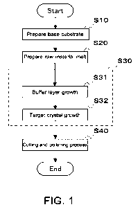
[0011]
Fig. 1 shows a flowchart of the production method for a
bismuth-substituted rare earth iron garnet single crystal.
Description of Embodiments
[0012]
Hereinafter, embodiments of the present invention will
be described in detail, but the present invention is not limited
thereto.
[0013]
CA 03183695 2022- 12- 21
5
In this embodiment, in growing single crystal film,
especially bismuth-substituted rare earth iron garnet crystal,
by epitaxial method on a crystal substrate, a buffer layer with
a large rate of lattice constant change is initially formed on
the substrate surface, and then the target garnet film is grown
with a low rate of lattice constant change. By forming the
buffer layer, it is possible to reduce the occurrence of cracks
and other problems during thick film growth. Details are
described below.
[0014]
<Composition of bismuth-substituted rare earth iron garnet
single crystal>
The bismuth-substituted rare earth iron garnet single
crystal produced by the production method of the present
embodiment will be described. This bismuth-substituted rare
earth iron garnet single crystal is suitable for use in a Faraday
rotator and an optical isolator. The bismuth-substituted rare
earth iron garnet single crystal is represented by the following
compositional formula (1) .
(Ln3-aBia) (Fe5-bAb) 012 . . . ( 1)
[0015]
In the composition formula (1) , Ln is one or more elements
selected from Y, lanthanides (La, Ce, Pr, Nd, Sm, Eu, Gd, Tb,
Dy, Ho, Er, Tm, Yb, Lu) , and trace elements such as Ca, Mg, Zr.
Multiple of these elements may be used as Ln simultaneously.
A is selected from Al, Ga, In, Sc, and Hf or trace elements such
as Ti, Si, Ge, and Sn. Multiple of these elements may be used
as A simultaneously.
CA 03183695 2022- 12- 21
6
[0016]
<Production method of bismuth-substituted rare earth iron
garnet single crystal>
The bismuth-substituted rare earth iron garnet single
crystal of the present invention may be grown with a Pb0-free
melt composition. A specific example of the production method
of bismuth-substituted rare earth iron garnet single crystal
is explained below with reference to the flowchart shown in Fig.
1.
[0017]
First, a substrate used as a base for the growth of
bismuth-substituted rare earth iron garnet single crystal is
prepared (Step S10) . The substrate to be prepared may be a
paramagnetic garnet substrate with a lattice constant of Ls.
Specifically, for example, a Gd3Ga50i2 (GGG; gadolinium, gallium,
garnet) single crystal substrate with Ca, Mg, Zr, Y, etc. added
(NOG: Shin-Etsu Chemical trademark, SGGG: Saint-Gobain
trademark) may be used. By using such a substrate, a single
crystal can be pulled up and obtained by liquid-phase epitaxy.
[0018]
Next, the metal oxide that will be the raw material for
the bismuth-substituted rare earth iron garnet single crystal
is melted in a platinum crucible to prepare the raw material
melt (Step S20) . The raw metal oxides include, for example,
Gd203, Ho203, Bi203, Fe2O3, Ga203, TiO2, and MgO. The raw material
melt is prepared by preparing these metal oxides in
predetermined molar weight ratios, putting them in the platinum
CA 03183695 2022- 12- 21
7
crucible, and heating and melting them at a predetermined
temperature.
[0019]
Then, a single crystal film is grown by the liquid-phase
epitaxy in which the substrate is brought in contact with the
prepared raw material melt and pulling it up (Step S30) . In
the liquid-phase epitaxy method, the growth temperature is
gradually lowered to continuously separate a single crystal
film on the substrate surface. In the present embodiment, the
buffer layer is formed by a short time and large temperature
drop width in the early stages of growth (Step S31) . The average
lattice constant Lb of the buffer layer is larger than the
average lattice constant Ls of the base substrate, and the
thickness of the buffer layer is preferably 5 to 30 pm. Then,
the target crystal (garnet crystal film) is grown by a gradual
temperature drop over a long period of time (Step S32) . Thereby,
a garnet crystal film is formed overlaid on the buffer layer.
The average lattice constant Lf of the garnet crystal film is
larger than the average lattice constant Lb of the buffer layer,
and the thickness of the garnet crystal film may be more than
100 pm. The rate of lattice constant change (the amount of
change in lattice constant per unit length in the thickness
direction) in the buffer layer is steeper than the rate of
lattice constant change in the garnet crystal film. The rate
of lattice constant change in the buffer layer may be 10 x
10-4%/pm or more, and the rate of lattice constant change in
the bismuth-substituted rare earth iron garnet crystal film may
be 2.0 x 10⁻⁴%/pm or less.
CA 03183695 2022- 12- 21
8
[0020]
The grown single crystal film is then cut and polished
(i.e., the buffer layer and substrate are removed from the
bismuth-substituted rare earth iron garnet single crystal film)
to obtain the bismuth-substituted rare earth iron garnet single
crystal that can be used for a Faraday rotator and an optical
isolator (Step S40) . The Faraday rotator can be configured
using the bismuth-substituted rare earth iron garnet single
crystal thus obtained. Furthermore, the optical isolator can
be configured using the Faraday rotator.
[EXAMPLES]
[0021]
[Example 1]
Gd203, Ho203, Fe2O3, and Ga203 with Bi203 added as a flux
were melt heated at 1080 C in a platinum crucible, and then the
temperature was lowered to 815 C. The weight (melt
composition) of the raw materials to be melted were Gd203: 68
g, Ho203: 72.8 g, Fe2O3: 520.8 g, Ga203: 17.4 g, and Bi203: 7800
g, respectively.
[0022]
A 3-inch NOG substrate with a lattice constant of 12.498
A was immersed in the melt to start crystal growth, and the
temperature was further rapidly lowered by a temperature range
of 4 C in 1 hour, and then the substrate was brought out of
the melt. By this rapid temperature drop, a buffer layer was
formed. The crystal film of the buffer layer was 10 pm, and
the lattice constant of the film surface was 12.502 A (the
average lattice constant was 12.500 A). For the thickness
CA 03183695 2022- 12- 21
9
direction (perpendicular to the substrate surface), the rate
of change of the lattice constant was 32.0 x 10⁻⁴ %/pm.
[0023]
The substrate surface/crystal growth surface of the grown
crystals was polished, and each substrate surface/crystal
growth surface was coated with an antireflective coating
against air. Measured using a 1550-nm laser source, the
insertion loss was 0.08 dB, and when the effect of reflection
at the substrate-crystal interface was removed by calculation,
the insertion loss was 0.04 dB. This was a significant
insertion loss per unit length. Since the buffer layer has a
high loss, it is practical to use a Faraday rotor with the buffer
layer polished off, which is required for low insertion loss.
[0024]
The same initial melt composition as above was melt heated
to 1080 C, and then the temperature was lowered to 815 C. A
3-inch NOG substrate with a lattice constant of 12.498 A was
immersed in the melt to start crystal growth, and the
temperature was further rapidly lowered by 4 C in 1 hour. The
temperature was then gradually lowered by 10 C for 40 hours
to allow the crystal to grow. The total thickness of the crystal
grown in this way was 610 pm, and the thickness excluding the
buffer layer was 600 pm. The lattice constant of the film
surface was 12.510 A (the average lattice constant was 12.506
A) .
For the thickness direction (perpendicular to the
substrate surface), the rate of change of the lattice constant
was 1.6 x 10⁻⁴ %/pm. No cracking occurred until the film grew
to this thickness.
CA 03183695 2022 12 21
10
[0025]
The substrate and buffer layer were then polished and
removed from the grown crystal. The crystal growth surface was
then polished to 440 pm, corresponding to the Faraday rotation
angle of 45deg. Both sides of the polished crystal were coated
with antireflective coatings against air. The Faraday rotor
thus obtained was measured using a 1550-nm laser light source,
and the insertion loss was found to be 0.02 dB, which is a loss
without practical problems.
[0026]
[Comparative Example 1]
The initial melt composition as in Example 1 was melt
heated to 1080 C, and then the temperature was lowered to 815 C.
A 3-inch NOG substrate with a lattice constant of 12.498 A was
immersed in the melt, and the crystal was grown by gradually
lowering the temperature by 14 C for 42 hours from start to
finish. The total thickness of the crystal grown in this way
was 625 pm. The lattice constant of the film surface was 12.511
A (the average lattice constant was 12.507 A). Cracks were
observed at the outer periphery of the substrate in a crystal
grown in this way. Cracks were also observed when a crystal
with a total growth film thickness of 475 pm was grown in a
similar manner.
[0027]
[Example 2]
Gd203, Y203, Fe2O3, and Ga203 with Bi203 and B203 added as
a flux were melt heated at 1080 C in a platinum crucible, and
then the temperature was lowered to 812 C. The weight (melt
CA 03183695 2022 12 21
11
composition) of the raw materials to be melted were Gd203: 22.2
g, Y203: 44.4 g, Fe2O3: 512.4 g, Ga203: 14.0 g, Bi203: 7820 g,
and B203: 14.0 g, respectively.
[0028]
A 3-inch NOG substrate with a lattice constant of 12.497
A was immersed in the melt to start crystal growth, and the
temperature was further rapidly lowered by a temperature range
of 2 C in 0.5 hours, and then the substrate was brought out
of the melt. By this rapid temperature drop, a buffer layer
was formed. The crystal film of the buffer layer was 6 pm, and
the lattice constant of the film surface was 12.498 A (the
average lattice constant was 12.498 A). For the thickness
direction (perpendicular to the substrate surface), the rate
of change of the lattice constant was 13.3 x 10⁻⁴ %/pm.
[0029]
The same initial melt composition as above was melt heated
to 1080 C, and then the temperature was lowered to 812 C. A
3-inch NOG substrate with a lattice constant of 12.497 A was
immersed in the melt to start crystal growth, and the
temperature was further rapidly lowered by 4 C in 0.5 hours.
The temperature was then gradually lowered by 10 C for 56 hours
to allow the crystal to grow. The total thickness of the crystal
grown in this way was 575 pm, and the thickness excluding the
buffer layer was 569 pm. The lattice constant of the film
surface was 12.511 A (the average lattice constant was 12.505
A) .
For the thickness direction (perpendicular to the
substrate surface), the rate of change of the lattice constant
was 1.9 x 10⁻⁴ %/pm. No cracking occurred until the film grew
CA 03183695 2022 12 21
12
to this thickness.
[0030]
[Comparative Example 2]
As in Example 2, the initial melt composition was melt
heated to 1080 C, and then the temperature was lowered to 811 C.
A 3-inch NOG substrate with a lattice constant of 12.498 A was
immersed in the melt, and the crystal was grown by gradually
lowering the temperature by 12 C for 43 hours from start to
finish. The total thickness of the crystal grown in this way
was 595 pm. The lattice constant of the film surface was 12.512
A (the average lattice constant was 12.505 A) . Cracks were
identified in the crystal grown in this way. No cracks were
observed when a crystal with a total growth film thickness of
345 pm was grown in the same way, but cracks were scattered when
a crystal with a total growth film thickness of 425 pm was grown.
[0031]
[Example 3]
Eu203, Tb407, Fe2O3, and Ga203 with Bi203 added as a flux
were melt heated at 1090 C in a platinum crucible, and then the
temperature was lowered to 790 C. The weight (melt
composition) of the raw materials to be melted were Eu203: 21.5
g, Tb407: 174.0 g, Fe2O3: 525.5 g, Ga203: 24.0 g, and Bi203: 10570
g, respectively.
[0032]
A 3-inch NOG substrate with a lattice constant of 12.497
A was immersed in the melt to start crystal growth, and the
temperature was further rapidly lowered by a temperature range
of 6 C in 1.5 hours, and then the substrate was brought out
CA 03183695 2022 12 21
13
of the melt. By this rapid temperature drop, a buffer layer
was formed. The crystal film of the buffer layer was 30 pm,
and the lattice constant of the film surface was 12.502 A (the
average lattice constant was 12.500 A). For the thickness
direction (perpendicular to the substrate surface), the rate
of change of the lattice constant was 13.3 x 10⁻⁴ %/pm.
[0033]
The same initial melt composition as above was melt heated
to 1090 C, and then the temperature was lowered to 790 C. A
3-inch NOG substrate with a lattice constant of 12.497 A was
immersed in the melt to start crystal growth, and the
temperature was further rapidly lowered by 6 C in 1.5 hours.
The temperature was then gradually lowered by 12 C for 39 hours
to allow the crystal to grow. The total thickness of the crystal
grown in this way was 625 pm, and the thickness excluding the
buffer layer was 595 pm. The lattice constant of the film
surface was 12.512 A (the average lattice constant was 12.507
A) .
For the thickness direction (perpendicular to the
substrate surface), the rate of change of the lattice constant
was 1.9 x 10⁻⁴ %/pm. No cracking occurred until the film grew
to this thickness.
[0034]
[Comparative Example 3]
As in Example 3, the initial melt composition was melt
heated to 1090 C, and then the temperature was lowered to 789 C.
A 3-inch NOG substrate with a lattice constant of 12.498 A was
immersed in the melt, and the crystal was grown by gradually
lowering the temperature by 16 C for 41 hours from start to
CA 03183695 2022 12 21
14
finish. The total thickness of the crystal grown was 635 pm.
The lattice constant of the film surface was 12.513 A (the
average lattice constant was 12.506 A) . Cracks were identified
in the crystal grown in this way. No cracks were observed when
a crystal with a total growth film thickness of 345 pm was grown
in the same way, but cracks were scattered when a crystal with
a total growth film thickness of 500 pm was grown.
[0035]
As explained above, according to the present invention,
when the garnet single crystal film is deposited on the
substrate by the liquid-phase epitaxial method, stress
generation in the target single crystal layer can be reduced,
and cracking can be prevented.
[0036]
Although embodiments are described above, the present
invention is not limited to these examples. For example, in
order to control the ionic valence in garnet and to adjust the
lattice constant, small amounts of elements such as Ca, Mg, Zr,
and Hf may be added to Ln, and Al, Ga, In, Sc, Ti, Si, Ge, or
Sn may be added to A. In this way, the insertion loss can be
further reduced by controlling ion valence. Any addition,
deletion, or design modification of components as appropriate
by those skilled in the art to the aforementioned embodiments,
as well as any combination of features of each embodiment as
appropriate, are included within the scope of the invention as
long as they provide the gist of the invention.
CA 03183695 2022- 12- 21