Note: Descriptions are shown in the official language in which they were submitted.
1
PROGRAMMABLE MULTICORE PHOTONIC INTEGRATED CIRCUIT AND
RELATED OPERATION METHOD
5 DESCRIPTION
OBJ ECT OF THE INVENTION
The present invention relates to a programmable multicore photonic
integrated circuit comprising at least one programmable photonic modules or
10 cores,
and/or other photonic units like specific high performance blocks, capable
of implementing multipurpose signal processing, by the appropriate programming
of its resources, routing within the circuits and the blocks to achieve multi-
functional operation and the selection of its input and output ports. The
invention
also relates to a scalable programmable photonic integrated circuits arranged
in
15 a modular
multicore approach to increase the processing power of the overall
system and/or adding a multitude of functionalities enabled by complex
photonics
circuitry and parallelization as well as the related operation methods.
BACKGROUND OF THE INVENTION
20
Programmable multifunctional photonics (P MP) seeks to design common,
multipurpose configurations of integrated optical hardware that can implement
a
wide variety of functionalities by means of suitable programming a large set
of
reconfigurable basic processing elements or units. Various authors have
covered
theoretical works proposing different configurations and design principles for
25
programmable circuits based on cascade beam splitters or Mach-Zehnder
interferometers (MZIs). These proposals offer versatile hardware solutions to
implement programmable circuits, but none of them address the scalability
challenges that limit their evolution and practical use.
The performance of programmable multifunctional photonics and its capability
to
30
accomplish complex operations is proportional to the number of tuneable units
and basic processing elements that can be integrated. These architectures are
plagued by the similar limitations that integrated electronics faced in
connection
to the number of transistors per chip.
In the case of programmable multipurpose integrated photonic circuits, the
35
experimental demonstrations reported so far are mainly proof of concepts with
CA 03185883 2023-1- 12
8119030
2
small-scale integration of tuneable elements. The scalability limits arise
from: the
maximum number of basic units, which are in turn limited by the footprint and
the
reticle size of the lithography process employed, the accumulated losses
inside
the circuit and the optical interfaces, the capability to interface and
package a
5 large number of electronic ports and finally, the capability to interface
a large
number of optical ports.
Regarding the accumulated loss, even considering an unlimited quantity of
programmable unit cells, the maximum size of the circuit will be limited by
the
optical power loss due to propagation through the waveguides and components
10 inside the processor's core.
With respect to electrical interfacing the electrical routing of control
signals
imposes a system overhead that consumes a valuable portion of the design
footprint. In some cases, the distribution of routing tracks demands an
expanded
re-distribution of the optical components over the circuit to ensure the match
15 between the on-chip electrical layer and the optical layer. This creates
footprint
issues and limits the final integration density.
Inefficient programming can be found in large-scale single-core programmable
photonic processors when the use of peripheral high-performance building
blocks
is required. This issue arises when the location of the high-performance
building
20 blocks is not optimal for the required functionality and the signal is
forced to travel
relatively long distances through the core. This introduces additional losses
to the
circuit and increases the need for resources in the processor, which are
employed
just for internal interconnection purposes.
25 In order to mitigate the aforementioned limitations, a solution is
required to
scale the number of programmable unit cells in the circuit.
Multicore processors are well-known in the realms of electronics where
these architectures revolve around the utilization of two or more computation
units or cores placed in one single processor. The architecture rests on a
"divide
30 and conquer" strategy within a given clock cycle whereby when physical
limitation
presented scale up challenges, a "scale-out" approach was adopted [Add ref.,
10.1.1.637.5977, (Venu, 2011)].
In Photonic Integrated Circuits (P ICs) a few multicore architectures have
been proposed, mainly to implement interconnection networks on chip, which are
35 in turn applied to datacenters and transceivers. They employ different
types of
CA 03185883 2023-1- 12
8119030
3
cores: photonic cross-point matrix switches, photonic broadcast and select and
Wavelength Division Multiplexing (WDM) circuit routers, and electronic
processors.
5 1. Cross-point switches [(A. Shacham, 2007), (Luca Ramini, 2012)]:
This approach relies on the connection of cores implementing cross-point
switching matrices. Each "basic unit" of this approach is usually composed of
ring
resonators disposed in a matrix layout, with the basic unit present at each
node.
Some implementations also include the use of a multi-channel waveguide buses
10 that integrate wavelength division multiplexing operation.
2. Broadcast and select, WDM circuit routing [(T. Alexoudi, 2019), (Martijn
Heck,
2014)]:
This approach relies on using MUX-DEMUX devices like arrayed-waveguide
15 gratings and/or trees of directional couplers or MMIs along with
selective units,
which can be in the form of semiconductor optical amplifiers or ring
resonators.
3. Photonic assisted electronic multicore processors.
This approach relies on electronic processors interconnected by photonic
links.
20 To do so, the architecture requires photonic components to transition
from the
electronic domain to the optical domain (modulators) and photodetectors to
translate the signal from the optical domain to the electronic domain found in
each
core. The interconnection between electronic cores is done by means of a
photonic network through different techniques.
These approaches have a few attributes in common, viz.:
a. Photonic cores:
1. Are based on fixed application specific blocks (switching matrices,
30 and/or
demultiplexers) usually applied to network routing or optical
interconnects (i.e. not carrying any optical signal processing tasks).
2. Rely on switches rather than tuneable couplers i.e. both cores operate
over on/off digital states of 1 or 0 with the switch being on or off, while
intermediate states as in a coupler are not used.
35 3. Are
fixed and rigid in their layouts. While both can be used to route the
CA 03185883 2023-1- 12
8119030
4
channel selectively to various outputs, they cannot be used to perform
any other function or replicate any other circuitry as per demand.
b. Electronic cores:
1. Photonics is only employed to assist for the interconnection between
5 electronic cores.
2. Electro-optic and opto-electronic photonic components are required at
each interface with the electronic core.
DESCRIPTION OF THE INVENTION
10 The
object of the invention described here solves the scalability and
performance problems described above for programmable photonic integrated
circuits and allows the design and implementation of scalable programmable
photonic integrated circuits by means of a multi-core architecture where two
or
more programmable photonic cores and/or additional high performance blocks
15 are
interconnected, thus providing a clear technical advantage to current
approaches in term of ease of fabrication of large-scale circuits,
performance,
electrical/optical interfacing and scalability. In addition, the multicore
modular
approach enables fast and efficient setting of parallel and multitask
computations
and/or processing operations and the exploitation of their inherent
advantages.
20 The
object of the invention is based on the Interconnection of cores of
multipurpose programmable photonic processors. Each core includes a
reconfigurable optical waveguide mesh arrangement of photonic gates that
perform basic optical analog operations (reconfigurable optical power and
energy
division as well as independent phase shifting). In addition, each core can
include
25 a set of
high-performance photonic blocks specifically designed to perform
complex photonic and electro-optic operations. The combination and
interconnection of the previous components/resources defines a single module
or core. Therefore, and in view of the foregoing, it can be observed that the
present object of the invention allows one or various simultaneous photonic
30 circuits
and/or linear multiport transformations by means of suitably programming
of their resources, that is to say the corresponding programmable photonic
circuits of each core, and the input and output ports.
The invention relates to a programmable multicore photonic integrated
circuit comprising:
35 - at
least two photonic blocks, wherein at least one of the at least two
CA 03185883 2023-1- 12
8119030
5
photonic blocks is a programmable photonic core comprising:
i. a reconfigurable optical waveguide mesh arrangement of
photonic gates configured to perform optical analog
operations;
5 wherein the at least one programmable photonic core is configured to be
programmed and reconfigured to offer signal processing tasks either via non-
recursive, recursive or combined recursive and non-recursive signal
propagation.
Optionally, each of the at least one programmable photonic core further
10 comprises a set of internal high-performance photonic blocks configured
to
perform photonic and electro-optic operations.
Optionally, each of the at least one programmable photonic core further
comprises optical I/0s ports, wherein each of the at least one programmable
15 photonic core is connected to at least one programmable photonic core
via the
optical I/0s ports.
Optionally, each of the at least one programmable photonic core further
comprises a set of transition high-performance photonic blocks configured to
20 perform photonic and electro-optic operations and additionally to be
connected
to the opticals I/0s ports.
Optionally, each of the at least one programmable photonic core is
combined with a communication network configured to route the optical signals
25 from each of the at least one programmable photonic core.
Optionally, each of the at least one programmable photonic core is
connected to an adjacent programmable photonic core.
30 Optionally, each of the at least one programmable photonic core further
comprises an auxiliary switching or routing layer.
Optionally, each of the at least one programmable photonic core is
connected to a non-adjacent programmable photonic core.
CA 03185883 2023-1- 12
8119030
6
Optionally, each of the at least one programmable photonic core is directly
connected through at least one optical I/0s port to a distribution network.
Optionally, the distribution network connecting the at least one
5 programmable photonic core is configured to distribute dedicated routing
blocks
on every programmable photonic core.
Optionally, the distribution network connecting the at least one
programmable photonic core is configured to distribute dedicated routing
blocks
10 on a centralized subsystem.
Optionally, the at least one programmable photonic core is distributed over
a two-dimensional layer.
15 Optionally, the at least one programmable photonic core is distributed
over
three-dimensional stacked layers, each layer comprising one programmable
photonic core.
Optionally, the at least one programmable photonic core is distributed over
20 three-dimensional stacked layers, each layer comprising at least one
programmable photonic core.
Optionally, the programmable multicore photonic integrated circuit further
comprises optical connectors or couplers configured to enable an
interconnection
25 between the at least one programmable photonic core of the layer/s.
Optionally, the programmable multicore photonic integrated circuit further
comprises an integrated platform wherein the at least two photonic blocks are
physically interconnected.
Optionally, the at least two photonic blocks are optically and electrically
connected.
Optionally, the programmable multicore photonic integrated circuit further
35 comprises at least one optical power monitor wherein the at least one
CA 03185883 2023-1- 12
8119030
7
programmable photonic core is connected.
Optionally, the programmable multicore photonic integrated circuit further
comprises application-oriented blocks such as sensors, detectors, antennas,
5
measurement, transmission blocks, electronics ICs selected from DACs or ADCs,
drivers, monitors and/or amplifiers wherein the at least one programmable
photonic core is connected.
Optionally, the programmable multicore photonic integrated circuit further
comprises an electrical subsystem driving actuators or to on-chip
actuators/receivers, to an electrical subsystem monitoring the optoelectronic
read-outs and to an electronic processor or microprocessor that run the
optimization and configuration programs.
15
Optionally, the programmable multicore photonic integrated circuit further
comprises a control plane and/or software layer distributed over different
subsystems which is configured to control the at least one programmable
photonic core.
20
Optionally, the programmable multicore photonic integrated circuit further
comprises a control plane and/or software layer aggregated on a single system
which is configured to control the at least one programmable photonic core.
Optionally, each one of the at least one programmable photonic core is
25 connected to multiple adjacent programmable photonic core.
Optionally, the communication network is a dedicated communication
network configured to route the optical signals from each one of the at least
one
programmable photonic core.
Optionally, the communication network is a dedicated communication
network configured to allow the interconnection of programmable photonic core
with other non-adjacent programmable photonic core through the auxiliary
switching or routing layer.
CA 03185883 2023-1- 12
8119030
8
Optionally, the programmable multicore photonic integrated circuit is
implemented and integrated on a chip.
Optionally, the chip follows a homogeneous PIC integration where the at
5 least one programmable photonic core is integrated on a same substrate.
Optionally, the chip follows a heterogeneous PIC integration where the at
least one programmable photonic core is integrated on a same substrate.
10 Optionally, the chip follows an on board integration (chiplet-like)
approach
where a common substrate or a common platform is used to apply a plug-and-
play connection for laying out the at least one programmable photonic core
based
on a desired performance of a processor.
15 The invention also relates to a method of operating the programmable
multicore photonic integrated circuit described above, wherein the method
comprises connecting and utilising the at least one programmable photonic core
so that a signal from one programmable photonic core, enters to at least other
programmable photonic core, in a particular sequence where the programmable
20 photonic integrated circuit progress in series.
Optionally, the method comprises connecting and utilising the at least one
programmable photonic core so that a signal from one programmable photonic
core, enters to at least other programmable photonic core, in a particular
25 sequence where the programmable photonic integrated circuit splits and
process
the signals over the at least one programmable photonic core before its
combination on a different programmable photonic core.
Optionally, the method comprises programming the at least one
30 programmable photonic core to perform independent tasks at the same
time,
running in parallel.
The proposed photonic architecture based on the programmable multicore
photonic integrated circuit of the invention drastically increments the series
of
35 advantages inherent to field programmable photonic hardware approaches,
CA 03185883 2023-1- 12
8119030
9
expanded by the circuit topologies introduced by the invention. These include:
= Scalability of multipurpose programmable photonic circuits.
= Shorter times for production and to market.
= Lower prototype development and non-recurring engineering costs.
5 = Reduced financial risk in developing ideas and translating them into
ASP ICs.
= Multifunctional and multitask operation.
= Circuit optimization.
= Regular layouts and reduced footprints.
10 = Better yield and reproducibility of the Programmable Photonic Analogue
Blocks.
= Larger number of alternative circuit topologies not constrained by
geometrical factors.
= Programming of more complex and versatile circuits. Larger number of
15 ports i.e. inputs and outputs
= Enhanced functionality
= Improved optical and electrical interfacing.
= Better performance when programming larger and complex circuits.
= Reduction and mitigation of optical crosstalk and tuning crosstalk.
20 = Future scalability with minor design and verification cost.
The proposed based on the programmable multicore photonic integrated circuit
of the invention is suitable for the following applications:
= Aerospace and Defence (Avionics, Communications, Secure Solutions,
25 Space)
= Automotive (High Resolution Video, Image Processing Vehicle Networking
and Connectivity, Automotive Infotainment)
= Data Centers (Servers, Routers, Switches, Gateways)
= High Performance Computing (Servers, Super Computers, SIGINT
30 Systems, RADARs, Beam Forming Systems, Quantum computing, Neural
networks)
= Integrated Circuit Design (ASPIC Prototyping, Hardware Emulation)
= Wired and Wireless Communications (Optical Transport Networks,
Network Processing 5G Connectivity Interfaces, Mobile Backhaul)
35 = Hardware accelerators.
CA 03185883 2023-1- 12
8119030
10
= Machine and Deep learning applications.
= Artificial Intelligence
= Smart transceivers.
= Quantum photonic processors
Thus, the technical innovation proposed in this invention proposes the
architectures along with the workflows and control protocols of multicore
programmable photonic integrated processors that enable large-scale
integration
of programmable processing cells and can exploit the parallelization of
multiple-
tasks. It brings at the same time a considerable performance improvement when
compared to current architectures. It achieves improvement in functionality
with
respect to several factors, including, but not limited to, scalability,
performance
and multi-tasking efficiency.
The photonic cores of the present invention are not mere programmable
interconnection subsystems that can not be programmed and reconfigured to
offer signal processing tasks either via non-recursive or recursive signal
propagation. Thus, these cores leverage on the extra degree of freedom being
application agnostic. The overall device here can be defined as a
reconfigurable
network of reconfigurable signal processing cores.
DESCRIPTION OF THE DRAWINGS
In order to complement the description being made and with the object of
helping to better understand the characteristics of the invention, in
accordance
with a preferred practical embodiment thereof, said description is
accompanied,
as an integral part thereof, by a set of figures where, in an illustrative and
non-
limiting manner, the following has been represented:
Figure 1 shows a non-limitative example of a schematic diagram of the
proposed photonic architecture of the invention, wherein the illustration
shows an
implementation example of a Multicore with seamless interconnect.
Figure 2 shows a non-limitative example of a schematic diagram of the
proposed photonic architecture of the invention.
Figure 3 shows non-limitative examples of schematic diagrams of the
proposed photonic architecture of the invention.
Figure 4 shows a non-limitative example of a schematic diagram of the
CA 03185883 2023-1- 12
8119030
11
proposed photonic architecture of the invention.
Figure 5 shows a non-limitative example of a schematic diagram of the
proposed photonic architecture of the invention.
Figure 6 shows a non-limitative example of a schematic diagram of the
5 proposed photonic architecture of the invention.
Figure 7 (left) shows a non-limitative example of a schematic diagram of
the proposed photonic architecture of the invention. Figure 7 (right) shows a
non-
limitative example of a schematic diagram of the proposed photonic
architecture
of the invention.
10 Figure 8 shows a non-limitative example of a schematic diagram of the
proposed photonic architecture of the invention.
PREFERRED EMBODIMENT OF THE INVENTION
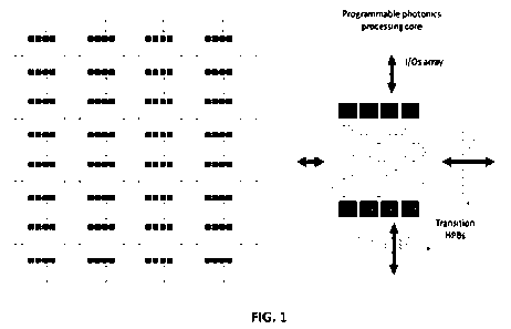
15 In a preferred embodiment of the object of the invention, a device is
provided as
shown in Figure 1 where a set of at least two, but preferably a large number
of
multipurpose programmable photonic circuits are aggregated and connected in
modules or cores, where each module or core of programmable photonic
integrated circuit is used in conjunction with other programmable photonic
20 circuits, or additional functional blocks which can be high performance
blocks,
specific functionality blocks or other such units. These blocks have
programmable characteristics and perform optical signal processing on a
photonic chip. Take into account that the design in Figure 1 does not assume
any
particular interconnection geometry or topology for the multipurpose
25 programmable photonic circuit present at each core or module and that
the
resulting design shown there is only for the purposes of illustration.
Although
various subcore architectures may be considered, here we are illustrating the
design with a very basic hexagonal waveguide mesh connected to a set of 8 high-
performance building blocks and transition high-performance building blocks.
30 Figure 1-3 shows examples of the possible interconnection and
architecture
options but they are not limited to only these examples. In particular, the
scheme
of said multipurpose multicore programmable photonic processor is shown in
Figure 1 for a particular Multicore with seamless interconnect architecture.
In this
architecture, each processing core is connected with up to 4 neighbouring
cores
35 through its optical I/0s ports. The replication and interconnection of
this module
CA 03185883 2023-1- 12
8119030
12
with its neighbouring cores leads to a straightforward processing network
being
characterized by its simplicity, scalability, design costs and versatility.
Some
designs variations can incorporate high-performance building blocks placed in
the optical interface to perform specific functions including but not limited
to
5 optical signal amplification and nonlinear operations.
In some cases, it is beneficial to access the cores without the need to
accessing directly to its internal resources or to have a hardware which can
support both as required through a software control. Figure 2 shows a non-
limitative example of a schematic diagram of the proposed photonic
architecture
10 of the invention, wherein the illustration shows an implementation
example of an
implementation of Multicore with distributed interconnect. In this
architecture,
each processing core is combined with a communication network that routes the
optical signals from each modular core. The replication and interconnection of
this module with its neighbouring cores leads to an on-chip communication and
15 processing network characterized by its efficiency, scalability, design
costs and
versatility. This architecture works similarly to the Field-Programmable
Photonic
Gate array architecture, where large quantities of general processing
resources
are accessible to the user. As in the previous approach, the design has no
centralized resource that can get larger and more complicated as the number of
20 cores increase. Thus, design complexity and verification complexity are
independent of core count.
The previous two approaches do not allow the direct interconnection of
cores that are not adjacent one to another. Figure 3 shows a non-limitative
example of a schematic diagram of the proposed photonic architecture of the
25 invention, wherein the illustration shows an implementation example of a
Multicore with centralized interconnect. This scheme allows the
interconnection
of a given core with other non-neighbouring cores employing an auxiliary
switching/routing layer. This design is interesting in multicores with a
reduced
number of cores, but it comes at the cost of scalability issues and require
30 additional verification and customization for each hardware upgrade.
By means of suitably programming each core or module, the multipurpose
multicore programmable photonic processor can implement complex
autonomous and/or parallel photonic circuits and signal processing
transformations by discretizing complex optical processing circuits into
different
35 interconnected modules of programmable photonic processors. The goal
then is
CA 03185883 2023-1- 12
8119030
13
to achieve a functional advantage given by the modular approach and increase
the performance, scalability, versatility and adding novel higher processing
capabilities.
In particular, the invention is illustrated in Figures 4-6, where it is shown
5 how complex optical signal processing circuits can be configured by means
of
the programming of the proposed device. In particular, we show how the
Multicore with seamless interconnect architecture programs a complex circuit
distributed in 4 cores, the capabilities of adding sections of the circuit
working in
parallel, and the capability to perform independent multitask operations.
10 The multipurpose multicore programmable photonic processor combines
the programmability of the basic programmable photonic processors in a
scalable
interconnection structure, allowing programmable circuits with scalable
processing capabilities and with added functionalities like enhanced circuit
parallelization. Thus, processing complexity comes from the interconnectivity
15 internal to the core and between cores. In addition, it solves the major
problems
related to the scalability of programmable photonic circuits, where increasing
the
density of its programmable unit cells comes at the cost of adversarial
effects like
optical crosstalk, tuning crosstalk, non-scalable optical and electrical
interfacing
and limited footprint for fabrication processes. Multicore programmable
photonic
20 processor architectures include the interconnection of several general-
purpose
cores and arise as an elegant solution to scale the performance of
conventional
photonic processors. Since the scalability limits of single-core processors is
exacerbated when a larger number of programmable unit cells are integrated in
the circuit, a straightforward approach is to use an architecture that
integrates
25 and interconnects several smaller cores.
The control of this whole device including all the interconnected blocks can
either
be carried out using the individual software for driving each core or can be
added
into one software interface leading to a common mean to drive, program,
control
30 and re-configure the whole hardware. A common software enables the smart
programming and management of resources to achieve optimal configurations in
terms of number of components employed, power consumption, programming
efficiency, mitigation of side effects (optical and tuning crosstalk).
35 OPERATION EXAMPLES
CA 03185883 2023-1- 12
8119030
14
The disaggregated nature of multicore photonic processors enables a wide set
of
modes of operations. In this section we illustrate some non-limiting examples:
Figure 4 shows a schematic of Programming of progressively distributed
circuits (Serialization) wherein the illustration shows a configuration
example of a
Multicore with seamless interconnect where a complex circuit is programmed
over 4 cores following a serial circuit. The circuit includes the programming
of
(first core) ring resonator, dispersive delay in a high-performance building
block,
optical amplifier in a transition HPB, (second core) an optical splitter, a
beamforming network, (third core) a 6th order Finite Impulse Response Filter,
and
(fourth core) a branch with an optical attenuator implemented by a high-
performance building block and a branch with a high-q filter and a
polarization
filter. The configuration of complex photonic circuit on a single-core
processor is
limited by the number of optical ports, programmable unit cells and high-
performance blocks available in the circuit. In addition, the accumulation of
non-
ideal effects (optical and crosstalk during phase tuning), and the large
number of
required programmable unit cells to perform complex operations might rapidly
limit the circuits that the inner core can implement. Figure 4 illustrates how
the
multicore architecture divides and distributes the circuit into the cores. The
programmed circuit does not target any application and is merely set to
highlight
the main capabilities of this mode of operation. In this case, the first core
(top left)
configures an optical ring resonator in the inner core, accesses a dispersive
delay
provided by the HPB 7 and amplifies the optical signal before connecting to
the
next core. The next core (top right) splits the optical signal into two paths.
The
first path feeds a programmed optical beamformer, demonstrating the benefits
of
the multicore approach for circuits that require multiple optical paths and
ports.
The other path is directed to the interconnected output to access the third
core.
The third core (bottom right) implements an optical lattice filter in its core
based
on three unbalanced MZIs and directs the two outputs of the filter to the next
and
the last core. The last core (bottom left) distribute one of the optical
interconnections to an optical attenuator and the other optical connection to
a
cascade of an HPB filter and a polarization filter, respectively.
Figure 5 shows a schematic of Programming of parallelly-distributed
circuits (Parallelization) wherein the illustration shows a configuration
example of
a Multicore with seamless interconnect where a complex circuit is programmed
over 4 cores following a parallel circuit. The circuit includes the
programming of
CA 03185883 2023-1- 12
8119030
15
(top left core) Mach-Zehnder Modulator, and optical splitter and an optical
amplifier, (top right core) an optical filter with two outputs, (bottom left
core) an
optical filter based on an MZI and four ring resonators, and (bottom right
core) a
combiner, and a photodetector. Some circuits include circuit divisions into
blocks
5 that run in parallel. Although possible in single-core processors, the
programming
of these circuits can be limited when programmed in single cores individually.
In
this case, the interference between the branches of the circuit that run in
parallel
can reduce the overall processing performance. In order to mitigate this
effect,
multicore-architectures can distribute sections of the same circuit that run
in
10 parallel over different processing cores. Figure 5 illustrates the
programming of a
circuit distributed over 4 cores. The first core (top left) gets the input
signal and
access to a MZI modulator before splitting and routing it to the second (top
right)
and third (bottom left) core. Each core contains a different optical filter.
In the first
case it is a third-order ring resonator architecture that extracts the
passband and
15 feeds it onto the fourth core (bottom right) and the stopband or
reflection response
to an external port. The second case (bottom left) is an optical filter that
combines
lattice filters and optical ring resonators before directing the two output
ports to
the fourth core. The last core (bottom right) receives the signal from two
different
cores. The signal coming from the bottom-left core is detected using a high-
speed
20 photodiode block. The second signal coming from the bottom left core is
combined with the optical signal coming from the top-right core before
accessing
to the optical output port.
Figure 6 shows a schematic of Programming independent circuits
(Multitask) wherein the illustration shows a configuration example of a
Multicore
25 with seamless interconnect where two independent complex circuit are
programmed over 4 cores following multitasking operation. The circuit includes
a
cascade of two unitary blocks with an intermediate nonlinear section (top
cores)
and another cascade of a filtering section of 4 rings in an array followed by
a 4x4
multiport interferometer. The last key advantage of multicore photonic
processors
30 resides in their capability to perform independent tasks at the same
time. This
capability can be exploited on single-core processors as well, but additional
optimization techniques need to be applied to mitigate the crosstalk between
both
circuits. In short, the processor programs two or more circuits running in
parallel
and performing independent tasks. The circuits can be of the same or a totally
35 different design. In addition, the circuits can be distributed over
different cores or
CA 03185883 2023-1- 12
8119030
16
can be programmed to share some of the resources available on the same core
for the cases including but not limited to exigent applications. Figure 6
illustrates
an example where the multicore architecture programs two independent circuits.
The upper cores configure a two-layer neural network of 6 modes. The cores
5 located at the bottom of the processor configure an initial filtering
stage before
accessing to a 4x4 interferometer followed by a non-linear array.
PHYSICAL IMPLEMENTATION
The physical implementation of the MULTIPURPOSE MULTICORE
PROGRAMMABLE PHOTONIC PROCESSOR calls for an integrated optics
approach either based on silicon photonics platform and/or a
hybrid/heterogeneous III-V, and/or group IIV-Vs and/or barium-titanate and/or
15 any other chalcogenide and/or II-VI platform. It is not only limited to
the integration
of programmable photonics ICs with other photonics ICs and/or blocks but also
with electronics ICs and subsequent blocks of such nature.
As for the programmable photonic blocks, the currently available photonics
technology options are based on any phase or amplitude tuning effect like:
20 MEMS, thermo-optic effects, electro-optic effects, opto-mechanics,
electro-
capacitive effects or non-volatile phase actuators. This phase shifters and
actuators are integrated in any interferometric structure with two or more
ports.
Different architecture and integration levels are included in the physical
25 implementation which can be classified as follows:
ARCHITECTURES:
Heterogeneous architectures: Although one of the key advantages of multicore
architectures is the replication of the same unit core, the range of
applications
30 can be expanded if each core employs different HP Bs as well as inner
core
topologies. As an illustrative example Figure 7(left) shows a configuration
example of a Multicore with seamless interconnect with a heterogeneous
architecture where 4 cores have a different internal composition. In
particular,
each core includes a set of high-performance processing blocks and a different
35 waveguide mesh arrangement (hexagonal, triangular, square and
feedforward).
CA 03185883 2023-1- 12
8119030
17
That is to say, it is a 4-core architecture with different inner cores for
each module:
hexagonal mesh architecture, triangular mesh architecture, square mesh
architecture and a rectangular multiport interferometer. Note as well, that
each
one can integrate different H PBs. The key advantage of this implementation
5 resides on the availability of specific resources required by some
applications.
For example, the feedforward mesh illustrated in the bottom right core can be
implemented by the hexagonal mesh, but in a less efficient way.
2D architectures: 2D architectures can be implemented considering the current
10 standards and state of PIC and their integration. The 2d architectures
would most
commonly come across as connecting a chip to another in the photonic
equivalent of making a "short" through connecting optical fibres or waveguides
coming off from the different chips. This can be done with a singular package
of
different photonics chips on the same or different integration platforms.
3D architectures (single and multi-core): Figure 7(right) shows a 3D
architecture
with 4 cores, each one connected to their neighbours through vertical
interconnections. That is to say, it is a multicore with seamless interconnect
programming 4 cascaded circuits on a 3D integration shape. The connections
20 between cores are done by waveguide couplers designed to couple the
light in
the vertical direction to an upper/lower waveguide layer.
3D stacking architectures rely on placing multiple cores in a 3D layout (as
shown
in Fig. 7 for performance enhancements in relation to the processing power.
Single core designs are limited in its scalability by the reticle size of the
fabrication
25 tools. Such core, post-assembly can be individually stacked together to
form
multiple cores to overcome such limits but then the form factor is
compromised.
A solution in which can drastically reduce the form factor while showing a
manifold increase in the performance is 3D stacking whereby such cores are
placed in layer stacks one on top of each other with interconnections running
30 through each to form a larger and more functionally potent unit. The
stacking can
be set in parallel to aid parallel processing leading to the possibility of
performing
functionalities in parallel.
A mixed architecture of 2D and 3D multicores can also be implemented.
CA 03185883 2023-1- 12
8119030
18
INTEGRATION LEVEL:
On chip integration: On-chip integration implies that the photonic core is
connected to neighbouring cores or additional functional blocks with all the
core
5 and elements being in the same substrate. The on-chip integration can be
carried
out in a multitude of approaches with the most common one's listed below:
= Homogeneous PIC Integration: In this approach, all the cores are realized
on the same fabrication run on a single die of the PIC. Multiple cores can
10 be implemented in such an approach and the key advantage of
homogenous integration comes from the very small form factor that can
be achieved. Single core implementation in programmable PICs are
limited by the sheer geometric constraints presented by the size of the
reticle. In this approach as presented in the present invention, a non-
15 limiting example is a multicore processor formed by fabricating the
same
core across a single wafer and with one or more cores core being defined
as the unit fabricated in one reticle. All or some of the different segments
of the wafer with the core(s) defined in a reticle are then left
interconnected
i.e. the different dies are not cleaved but left as a conglomerate
20 interconnection of multiple dies with cores to give rise to a
multicore
processor where all the cores are defined and set purely during fabrication
thus negating the need for interconnection of the different cores during
packaging. This approach then relaxes the demands on PIC packaging
and increases the throughput and facilitates the hardware realisation
25 through a more simplistic process flow.
Heterogeneous PIC Integration: Heterogenous PICs revolve around the
integration of two or more different materials on the same chip substrate.
The most common executions of such approach can be seen with active
30 devices in I nP integrated with small form factor SOI circuits or low
loss SiN
platform but can even extend to other materials such a Barium Titanate
(BTO), graphene, chalcogenides, etc. As a photonic gain medium does
not exist in pure SOI or SiN circuit, this adds a great deal of functionality,
including but not limited to, integration of on-chip laser as well as gain
35 elements which can then in turn aid in achieving several multi-core
CA 03185883 2023-1- 12
8119030
19
architectures. The implementation in itself is reliant on a thin layer of InP
or other III-V material being "attached" in specific sections, on top of a SOI
or SIN chip. The light, at these sections is evanescently coupled from the
SOI or SIN waveguides into the InP sections to induce gain or as an
5 efficient phase modulation sections. The process of "attaching" is
then
carried out through means like BCB or other polymers by wafer bonding
techniques or can involve other means such as micro-transfer printing.
On board integration (chiplet-like): The basis of this implementation is to
divide
10 chip design (co-design) and fabrication based on their basic
functionality, so for
example, that can come in the form of functional sub-system blocks like the
core,
active blocks like lasers and gain medium, non-linear blocks, etc. After these
said
blocks have been manufactured and the sub-assembly (individual chip
packaging) has been done, they will be placed on a platform which is an
15 interlinked substrate and then packaged into a single unit. Chiplets
address the
fact that there's no one-size-fits-all approach that works to meet current
demands.
This implementation is not only limited to the aggregation of photonic
multipurpose photonic blocks and/or other high-performance photonics blocks
but can also include pure electronic blocks including but not limited to
drivers,
20 monitors, ADCs, DACs, amplifiers, sensors and antennas.
Figure 8 shows a non-limitative example of a schematic diagram of the proposed
photonic architecture of the invention, wherein the illustration shows an
implementation example of a implementation of said MULTIPURPOSE
PROGRAMMABLE PHOTONIC PROCESSOR in a multicore layout were each
25 core can be connected in a plug-and-play or chiplet-like approach
whereby a
common platform shown in green is used to interconnect two or more
programmable photonic blocks with other programmable photonic blocks or
functional units. All these units are represented in the schematic as black
boxes
as they can include two or more programmable PICs and/or photonic high
30 performance building blocks which can be further extend to include pure
electronic ICs such as drivers, monitors, ADCs, DACs, sensors, antennas, etc.
In addition, all the previous implementations can employ a control and driving
subsystem to enable the control and driving of the multipurpose multicore
CA 03185883 2023-1- 12
8119030
20
programmable photonic processor. The control and driving circuitry enable the
extraction and reading of optical signals and the driving of the photonic
actuators.
CA 03185883 2023-1- 12
8119030