Note: Descriptions are shown in the official language in which they were submitted.
METHOD FOR PRODUCING A MICROOPTOELECTROMECHANICAL
COMPONENT, AND CORRESPONDING MICROOPTOELECTROMECHANICAL
COMPONENT
[0001] The present invention relates to a method for producing a
microoptoelectromechanical component and to a corresponding
microoptoelectromechanical
component.
Prior art
[0002] Photonic devices integrated into microelectromechanical
elements (M EMS)
belong to the next generation of communications and sensor systems. Thanks to
the MEMs
processes and the silicon-on-insulator (S01) technology, the miniaturization
of many elements,
such as lenses, mirrors, beam-splitters, gratings, filters, low-loss
waveguides, multiplexers, and
light switches, is possible, for example. These elements belong to the
category of
microoptoelectromechanical systems (MOEMS) and the reconfigurable optical
add/drop
multiplexers (ROADMs).
[0003] Optical light switches are currently being developed that
are compatible with
MEMs technology and produced with semiconductor processes, e.g., as optical
transceivers for
the 5G network.
[0004] Three relevant components are required for these optical
light switches:
[0005] Optical waveguides, which are typically produced from
three deposited layers. An
upper and a lower layer, also referred to as the bottom clad and top clad,
consist of silicon oxide
-1-
CA 03185931 2023- 1- 12
with a refractive index of approximately 1.45. A middle layer referred to as
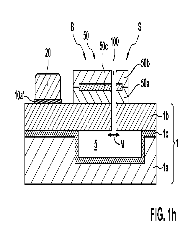
the core consists of a
material, typically silicon nitride, with a higher refractive index than the
bottom and top clads.
The layers are structured by photolithography so that the two clads completely
wrap around the
core. The optical waveguide is divided into a stationary portion and into a
deflectable portion,
wherein the deflectable portion can be docked onto the stationary portion for
switching by
applying an electrical voltage.
[0006] Cavity SOI device wafer, on which the optical waveguides
are situated. A
substrate wafer, to which the SOI wafer is attached, has a hollow space, i.e.,
a cavity. If the
region above the cavity is processed by DRIE processes, this region is exposed
and can therefore
assume its MEMs function, specifically without the usual gas phase etching
processes, which,
without a cavity, would otherwise be necessary.
[0007] Metal contact pads, which are necessary for the
electrical drive of the MEMs
element and must have a perfect electrical contact between the MEMS substrate.
[0008] In the case of light switches, the optical waveguides are
constructed on SOI
wafers by CMOS processes. In order to expose the movable parts of the chip,
structuring of the
optical waveguides and of the lower SOI region is necessary. These two
structurings are referred
to as a "vertical etch" and "DRIE trench."
[0009] In order to reduce the optical losses, the movable
portion of the waveguide must
dock very well on the stationary portion, which is why the walls of the
optical waveguide must
be as perpendicular as possible in this switching region. Since the thickness
of the optical
waveguide is several micrometers, the use of a soft mask (lacquer mask) is not
sufficient to
reproduce the required vertical flanks.
- 2 -
CA 03185931 2023- 1- 12
[0010] Since the traffic volumes transmitted by
telecommunications networks have
increased rapidly due to the bandwidth-intensive applications such as Internet
access, multimedia
applications for electronic commerce, and distributed computing, it is
absolutely necessary to use
the optical network for backbone, metropolitan, and local networks and
regional networks. The
optical networks using optical fibers as a transmission medium have shown a
superior
performance/cost ratio for both long-distance and short-distance routes, and
the up-and-coming
DWDM/all-optical networks (densight wavelength division multiplexing) have
shown a
promising improvement potential, speed, capacity, and connectivity of optical
telecommunications networks.
[0011] US 2004/0264847 Al discloses a microoptoelectromechanical
waveguide switch
(MOEM-WS) constructed by integrating MEMS actuators and microPLC on the same
substrate.
The MOEM-WS is an integrated hybrid microsystem: the
microoptoelectromechanical system
(MOEMS) is suitable in particular for optical cross-connect switches (OXC) and
optical
add/drop multiplexers (OADM). The MOEM-WS offers a significant fiber-switching
capability
for purely optical networks, with numerous advantages associated therewith,
such as low costs,
low crosstalk, reliability, compactness, high speed, reconfigurability,
modularity, scalability, and
insensitivity to signal wavelength and polarization.
Disclosure of the invention
[0012] The present invention relates to a method for producing a
microoptoelectromechanical component according to claim 1 and to a
corresponding
microoptoelectromechanical component according to claim 10.
- 3 -
CA 03185931 2023- 1- 12
[0013] The idea underlying the present invention is to use a
multilayer hard mask for the
"vertical etch."
[0014] Preferred developments are the subject matter of the
dependent claims.
Advantages of the invention
[0015] The production method according to the invention enables
the formation of very
perpendicular lateral walls of the trench that separates the stationary and
the deflectable portions.
The electrically conductive, first hard mask layer simultaneously enables good
electrical
connection of the electrical contact element to the covering substrate via the
contact pad
remaining from it.
[0016] According to a preferred embodiment, an insulation layer
is applied to the base
substrate and extends into the cavity. This allows direct bonding from the
covering substrate to
the base substrate.
[0017] According to a further preferred embodiment, the base
substrate and the covering
substrate are a silicon substrate.
[0018] According to a further preferred embodiment, the first
hard mask layer is a doped
polysilicon layer, and the second hard mask layer is a silicon oxide layer.
Thus, a desired etching
selectivity to the optical waveguide can be achieved.
[0019] According to a further preferred embodiment, the
formation of the etching
opening is carried out using a lacquer mask.
[0020] According to a further preferred embodiment, the optical
waveguide core is
formed from silicon nitride and is sheathed by a lower covering layer and an
upper covering
layer made of silicon oxide. Good optical waveguide properties can thus be
achieved.
- 4 -
CA 03185931 2023- 1- 12
[0021] According to a further preferred embodiment, trench
etching is carried out in a
two-stage etching process in which the optical waveguide is trenched in a
first etching step, and
the covering substrate located therebelow is trenched in a second etching
step. The etching
process for the respective material can thus be optimized.
[0022] According to a further preferred embodiment, the second
hard mask layer is at
least partially removed in the first etching step.
[0023] According to a further preferred embodiment, the
electrical contact element is
produced from aluminum. This enables a low-resistance coupling of the movable
MEMS portion.
Brief description of the drawings
[0024] The present invention is explained in more detail below
based upon the exemplary
embodiments indicated in the schematic figures of the drawings. In the
drawings:
[0025] Fig. la)-h) show schematic cross-sectional views for
illustrating a
microoptoelectromechanical component and a corresponding production method
according to
one embodiment of the present invention.
Embodiments of the invention
[0026] In the figures, identical reference signs denote
identical or functionally identical
elements.
[0027] Fig. la)-h) show schematic cross-sectional views for
illustrating a
microoptoelectromechanical component and a corresponding production method
according to
one embodiment of the present invention.
- 5 -
CA 03185931 2023- 1- 12
[0028] In Fig. la), reference sign 1 denotes an SOI substrate,
which has a base substrate
la having a cavity 5 which is formed therein and is closed by a covering
substrate lb. The
covering substrate lb is, for example, bonded by SOI direct bonding to an
insulation layer lc,
which is made of silicon oxide, applied to the base substrate la, and extends
continuously into
the cavity 5.
[0029] An optical waveguide 50 is formed on the covering
substrate lb above the
cavity 5 and has a sheathed waveguide core 50c. The optical waveguide core 50c
is formed, for
example, from silicon nitride and is sheathed by a lower covering layer 50a
and an upper
covering layer 50b, each made of silicon oxide.
[0030] Furthermore, with reference to Fig. lb), an electrically
conductive, first hard mask
layer 10a is formed above the optical waveguide 50 and the surrounding
covering substrate lb
and consists, for example, of a doped polysilicon layer.
[0031] Subsequently, according to Fig. 1c), a metallization,
e.g., of aluminum, is
deposited over the first hard mask layer 10a and is structured into an
electrical contact
element 50 on the first hard mask layer 10a in the region of the surrounding
covering
substrate lb.
[0032] As shown in Fig. 1d), a second hard mask layer 10b is
subsequently applied over
the first hard mask layer 10a and the electrical contact element 20 and
consists, for example, of
silicon oxide.
[0033] According to Fig. le), an etching opening 11 is
subsequently formed in the first
and second hard mask layers 10a, 10b for the purpose of partially exposing the
upper side of the
optical waveguide 50. This formation of the etching opening 11 can take place,
for example,
using a lacquer mask (not shown).
- 6 -
CA 03185931 2023- 1- 12
[0034] According to Fig. if), after removal of the lacquer mask,
trench etching of the
optical waveguide 50 is carried out in a first etching step. This first
etching step stops, for
example, on the underlying covering substrate lb and creates a partial trench
100a.
[0035] According to Fig. 1g), in a subsequent second etching
step, the covering
substrate lb located below the partial trench 100a is trenched up to the
cavity 5 in order to create
a continuous trench 100. This continuous trench 100 divides the optical
waveguide 50 and the
covering substrate lb located therebelow into a stationary portion S and into
a deflectable
portion B, as explained in more detail below.
[0036] Subsequently, according to Fig. 1h), the exposed first
and second hard mask
layers 10a, 10b are removed, wherein, below the electrical contact element 20,
an electrical
contact pad 10a' formed from the electrically conductive, first hard mask
layer 10a remains.
[0037] During operation, the deflectable portion B can be docked
onto the stationary
portion S by electrically deflecting the corresponding portion of the covering
wafer lb, as a
result of which a light switch function can be achieved. The movement
direction is denoted in
Fig. 1g) and 1h) by reference sign M. The electrical deflection takes place,
for example, by
applying a corresponding control voltage to the electrical contact element 20.
[0038] Due to the used multilayer hard mask with the first hard
mask layer 10a and the
second hard mask layer 10d, it can be ensured that the vertical walls of the
continuous trench 100
are oriented as perpendicularly as possible such that full-area docking and
thus an exact light
switch function can be achieved.
[0039] The contact pad 10a' formed, below the electrical contact
element 20 made of
aluminum, from the first electrically conductive hard mask layer 10a ensures
good electrical
application of the electrical contact element 20 to the underlying covering
substrate lb.
- 7 -
CA 03185931 2023- 1- 12
[0040] Although the present invention has been completely
described above with
reference to preferred exemplary embodiments, it is not limited thereto, but
can be modified in
many ways.
[0041] In particular, the materials and structures specified are
indicated only by way of
example and not in a limiting manner.
- 8 -
CA 03185931 2023- 1- 12