Note: Descriptions are shown in the official language in which they were submitted.
90305458
- 1 -
Systems and methods for performing microscopic
analysis of a sample
Technical field of the invention
The present description relates to systems and methods for
microscopic analysis of a sample and relates in particular to the
microscopic analysis of a biological tissue, in particular skin.
Prior art
In the context of a dermatological examination in particular, it is
known to carry out a dermoscopic examination, that is to say an
observation of the surface of the skin using a magnifying optical
instrument, and then to carry out a local microscopic analysis
according to the observations made on the wide-field image obtained
by the dermoscopic examination.
The microscopic analysis comprises, for example, microscopic imaging
or spectroscopic analysis.
Among the imaging techniques, there are known in particular, and in
a non-limiting manner, confocal microscopy techniques such as, for
example, the technique described in Rajadhyaksha et al. [Ref. 1] or
K. Konig et al. [Ref. 2] for nonlinear microscopy. Also known are
techniques of optical coherence tomographic microscopy (0CM), in the
time domain (time domain OCM) or in the frequency domain (frequency
domain OCM). The known OCM techniques include techniques that combine
optical coherence tomography and confocal microscopy (see, for
example, Schmitt et al. [Ref. 3]) in order to improve lateral
resolution.
More specifically, the patent application W02015092019 [Ref. 4]
describes a technique of visualizing the internal structure of a
semi-transparent object arranged at the focus of a microscope
objective, for example a biological tissue, in order to obtain
vertical sections or B-scans orthogonal to the surface of the object,
at a high rate (several sections per second), with high
Date Recue/Date Received 2023-09-15
CA 03189741 2023-01-17
WO 2022/017784 - 2 -
PCT/EP2021/068661
spatial resolution, that is to say of the order of 1 pm,
both axially and laterally, and a satisfactory depth of
penetration, of the order of a millimeter. This technique
is based on optical coherence microscopy but has a
confocal filtering configuration that is linear or one-
dimensional (in one direction); for this, the
illumination line is optically conjugated, in particular
by means of the microscope objective, with a linear
detector, the detection area of which has a width
substantially identical to a width of the image of the
line, resulting in a spatial filtering of a region of the
object that is to be observed. Such a technique is thus
known as line-field confocal optical coherence tomography
(LC-OCT).
The article by Y. Chen et al. [Ref. 5] has also proposed
a line-scanning optical coherence tomographic microscopy
device, but one in which a sample is moved in a plane
perpendicular to an optical axis of the microscope
objective, and in a direction perpendicular to the
illumination line, making it possible to form en-face
images of the sample (or C-scans).
Among the techniques for spectroscopic analysis of a
sample, and in particular of a biological tissue such as
skin, there is known for example, and in a non-limiting
manner, Raman spectroscopy, which makes it possible to
form a molecular fingerprint of biological tissues, as
described for example in Schleusener et al. [Ref. 6]. The
review article by E. Drakaki et al. [Ref. 7] generally
presents different spectroscopy techniques applied to the
microscopic analysis of skin.
All of the microscopic analysis techniques described
above, whether for imaging or for spectroscopy, use a
microscope objective having a considerable nominal
numerical aperture, typically greater than or equal to
0.5, for a given field of view, typically of between
about 0.2 mm and about 1.5 mm.
In practice, in order to obtain relevant information
during the microscopic analysis, it is important for the
practitioner to find, during the microscopic analysis,
Date Regue/Date Received 2023-01-17
CA 03189741 2023-01-17
WO 2022/017784 ¨ 3 ¨
PCT/EP2021/068661
the zone that appears to him to be suspect in the image
obtained during the dermoscopic examination.
However, precisely finding in microscopic analysis a
suspect zone that has been identified in dermoscopy is a
complex matter, because the images on which it is
possible to rely for sighting are obtained on much
smaller fields than in dermoscopy, and they have a very
different appearance. This is even more critical when the
microscopic analysis does not produce images, such as in
Raman microspectroscopy for example.
Different solutions have been proposed to allow a
practitioner to identify, on the dermoscopic image, the
field of analysis for the microscopic analysis.
The patent application W02017139712 [Ref. 8] describes,
for example, a system which combines confocal microscopy
(or reflectance confocal microscopy (RCM)) and wide-field
dermoscopy (WFD). For this, a micro-camera is directly
integrated in the microscope objective in order to form
a surface image in wide-field reflection. However, such
a system is complex to manufacture and to integrate;
moreover, the images obtained by the micro-camera are of
poor quality.
The patent US7864996 [Ref. 9] describes a confocal
imaging system coupled with a dermatoscope. The
dermatoscope is mounted on a module fixed to the skin and
makes it possible to image the same zone as the confocal
microscope, which can be fixed on the same module. The
acquisition of a dermoscopic image (or "macroscopic"
image) is performed, followed by the acquisition of
confocal images. A precise correlation between the images
is made in order to represent, on the dermoscopic image,
the position of the image formed by the confocal imaging
system. However, the system thus described requires an
additional module for fixing two separate probes, and it
may be difficult for this module to be fixed at any
location on the skin. In addition, a complex procedure
must be followed for the acquisition of the images in
order to obtain the correlation of the dermoscopic and
confocal images.
Date Regue/Date Received 2023-01-17
CA 03189741 2023-01-17
WO 2022/017784 - 4 -
PCT/EP2021/068661
In the case of Raman microspectroscopy, Z. Wu et al. [Ref
10] describe how to acquire and localize micro-Raman
signals in tissues by means of reflectance confocal
microscopy imaging, and using a single laser source.
However, a confocal image is less easy to use, as a
reference image for a practitioner, than a dermoscopic
image.
The present description proposes microscopic analysis
devices and methods allowing a user to locate with
precision, and by means of a simple acquisition method,
the field of the microscopic analysis in a wide-field
surface reflection image, in which the image quality is
close to the quality of a dermoscopic image.
Summary of the invention
In the present description, the term "comprise" signifies
the same thing as "include", "contain", and is inclusive
or open and does not exclude other elements which are not
described or shown. Moreover, in the present description,
the term "about" or "substantially" is synonymous
with (signifies the same thing as) an upper and/or lower
margin of 10%, for example 5%, of the respective value.
According to a first aspect, the present description
relates to a system for microscopic analysis of a sample,
comprising:
a microscopic analysis path comprising:
a microscope objective of given nominal numerical
aperture in a given field of view;
an illumination path configured to illuminate the
sample through the microscope objective according to a
first illumination pattern and in a first spectral band;
a detection path comprising said microscope
objective, said detection path being configured to detect
in said field of view, and according to a detection
pattern, a light beam emitted by the sample in response
to said illumination of the sample, and to generate a
detection signal;
Date Regue/Date Received 2023-01-17
CA 03189741 2023-01-17
WO 2022/017784 ¨ 5 ¨
PCT/EP2021/068661
- a processing unit configured to generate
information on microscopic analysis of the sample from
said detection signal;
- a sighting path comprising:
- said microscope objective;
- a full-field illumination device configured to
illuminate the sample in a second spectral band;
- a two-dimensional detector;
- one or more imaging elements forming, with said
microscope objective, a full-field imaging device
configured to optically conjugate a given effective field
of the sample encompassing said field of view with a
detection area of the two-dimensional detector, and to
form a sighting image in surface reflection of said
effective field;
- a beam splitter element arranged upstream of the
microscope objective in order to separate the analysis
path and the sighting path;
- a display module configured to show said sighting
image and, on said sighting image, an image element
indicating the position of said detection pattern.
In the present description, the term "field of view" of
the microscope objective refers to a region of a focal
plane of the microscope objective, located in the object
space (sample space) for which the manufacturer
guarantees a nominal numerical aperture. A nominal
numerical aperture is, for example, between about 0.1 and
about 1.4, for example between about 0.5 and about 0.9.
The field of view can be defined by a circle with a
diameter of between about 100 pm and about 5 mm, for
example between about 500 pm and about 1.5 mm.
The term "effective field" of the microscope objective
is a field in the object space (sample space) which is
included in a total field of the microscope objective,
which encompasses said field of view and whose dimensions
are limited by the full-field imaging device of the
sighting path. The effective field can be defined by a
circle with a diameter of between about 1 mm and about
10 mm, for example between about 2 mm and about 5 mm.
Date Regue/Date Received 2023-01-17
CA 03189741 2023-01-17
WO 2022/017784 ¨ 6 ¨
PCT/EP2021/068661
In the present description, the illumination pattern
depends on the illumination path of the microscopic
analysis path and can comprise an illumination point, an
illumination line or an illumination surface, for example
a rectangular surface resulting from the scanning of an
illumination point or of an illumination line. An
illumination point is more precisely defined as the
diffraction pattern resulting from the focusing, by the
microscope objective of the microscopic analysis path,
of a collimated light beam incident on said objective.
The illumination pattern can also comprise an
illumination surface which does not result from scanning,
for example a surface with circular geometry, in the case
of a full-field microscopic analysis path. The light beam
emitted by the sample in response to the illumination of
the sample can be a reflected beam, a backscattered beam,
or a beam resulting from an emission process at another
wavelength (for example fluorescence, Raman scattering,
etc.).
Moreover, the detection pattern is included in the field
of view and is included in the illumination pattern or
is of the same order of magnitude, and depends on the
detection path of the microscopic analysis path. The
detection pattern can comprise a detection point, a
detection line or a detection surface, for example a
rectangular surface resulting from the scanning of a
line, or, in the case of a full-field microscopic
analysis path, a surface optically conjugated with a
detection area of a detector. A detection point is here
defined in the object space by an elementary zone
optically conjugated with an elementary detector of a
detector of the detection path of the microscopic
analysis channel.
The applicant has shown that the system for microscopic
analysis of a sample according to the first aspect allows
a user to precisely locate the field of the microscopic
analysis in a wide-field surface reflection image or
"sighting image". Said wide-field surface reflection
image can present an image quality close to the quality
Date Regue/Date Received 2023-01-17
CA 03189741 2023-01-17
WO 2022/017784 - 7 -
PCT/EP2021/068661
of a dermoscopic image due to the fact that the sighting
path is moved apart. However, the system retains very
good compactness compared to the systems of the prior art
that require two probes ([Ref 911 for example).
According to one or more exemplary embodiments, the full-
field imaging device of the sighting path has, in the
object space of the microscope objective, a numerical
aperture strictly lower than the nominal numerical
aperture of the microscope objective. It is then possible
for the sighting path to benefit from an effective field
greater than the field of view while limiting aberrations
and potential vignetting, while at the same time
maintaining limited dimensions for the imaging element(s)
forming the full-field imaging device. The quality of the
sighting image is therefore further improved.
According to one or more exemplary embodiments, said
sighting path further comprises a diaphragm making it
possible to limit the numerical aperture of the full-
field imaging device. According to other exemplary
embodiments, it is directly one of said imaging elements
forming the full-field imaging device that is configured
to additionally form a diaphragm for limiting the
numerical aperture of the full-field imaging device.
According to one or more exemplary embodiments, the full-
field imaging device of said sighting path is adjustable
in focusing. This makes it possible to form a sighting
image in surface reflection of the sample even when the
microscopic analysis path images deep into the sample
(case of OCM imaging for example).
According to one or more exemplary embodiments, the full-
field illumination device of the sighting path comprises
a plurality of light sources arranged on a periphery of
a distal face of the microscope objective, that is to say
the face of the microscope objective in the sample space.
This configuration permits direct illumination of the
sample. Alternatively, the full-field illumination
device of the sighting path can comprise a source
arranged upstream of the microscope objective and a beam
splitter element, for example a splitter cube, configured
Date Regue/Date Received 2023-01-17
CA 03189741 2023-01-17
WO 2022/017784 ¨ 8 ¨
PCT/EP2021/068661
to direct an illumination beam through the microscope
objective, toward the sample.
According to one or more exemplary embodiments, the
second spectral band differs at least partially from the
first spectral band, and said sighting path comprises
means for reducing the light power at least in said first
spectral band. In some cases indeed, an illumination beam
of the sample in the illumination path of the microscopic
analysis path can have a light power strong enough to
dazzle the detector of the sighting path. By reducing the
light power at least in said first spectral band, such a
risk of glare is limited.
According to one or more exemplary embodiments, the
second spectral band differs at least partially from the
first spectral band, and said beam splitter element
comprises a plate or a dichroic cube, configured to
separate the beams in each of said first and second
spectral bands. The dichroic plate then forms means for
reducing the light power in said first spectral band.
According to one or more exemplary embodiments, the
microscopic analysis path comprises a device for scanning
an illumination beam of the sample and a beam emitted by
the sample in response to said illumination of the
sample, and said beam splitter element forms part of the
scanning device.
According to one or more exemplary embodiments, said
image element indicating the position of said detection
pattern comprises a graphic element determined by means
of a prior calibration. This configuration is
particularly advantageous in particular when the
illumination pattern is not detected by the detector of
the sighting path, for example either because the
detector of the sighting path is not sensitive in the
first spectral band or because the first spectral band
in the sighting path is cut in order to limit glare. This
configuration is also advantageous when the illumination
pattern is difficult to identify in the sighting image,
or if the detection pattern is substantially different
from the illumination pattern.
Date Regue/Date Received 2023-01-17
CA 03189741 2023-01-17
WO 2022/017784 ¨ 9 ¨
PCT/EP2021/068661
According to one or more exemplary embodiments, said
microscopic analysis path is a confocal and/or optical
coherence tomographic imaging path, and said information
on microscopic analysis of the sample comprises at least
one image of the sample. For example, the microscopic
analysis path is an optical coherence tomographic imaging
path as described in the prior art and is configured to
form B-scans, C-scans (or en-face images) of the sample
or 3D images of the sample. In known manner, a cross-
sectional image of the sample, called a B-scan, is an
image formed in a plane parallel to the optical axis of
the microscope objective; a cross-sectional image of the
sample called a C-scan, or en-face image, is an image
formed in a plane perpendicular to the optical axis of
the microscope objective, and a 3D image of the sample
results from the acquisition of a plurality of B-scan
images or C-scans images and thus permits an analysis of
the sample in a volume.
According to one or more exemplary embodiments, said
microscopic analysis path is a spectroscopic analysis
path, and said information on microscopic analysis of the
sample comprises at least one spectrum of said light beam
emitted by the sample at at least one point of the sample.
According to a second aspect, the present description
relates to a method for analysis of a sample, comprising:
a microscopic analysis of the sample by means of a
microscopic analysis path comprising a microscope
objective of given nominal numerical aperture in a given
field of view, said microscopic analysis comprising:
-
illuminating the sample through the microscope
objective according to a first given illumination pattern
and in a first spectral band;
detecting in said field of view, and according
to a detection pattern, a light beam emitted by the sample
in response to said illumination of the sample in order
to form a detection signal;
processing said detection signal in order to
generate information on microscopic analysis of the
sample;
Date Regue/Date Received 2023-01-17
CA 03189741 2023-01-17
WO 2022/017784 - 10 -
PCT/EP2021/068661
- the formation of a sighting image in surface
reflection of a given effective field of the sample
encompassing said field of view, by means of a sighting
path comprising said microscope objective, a two-
dimensional detector, one or more imaging elements
configured to form with said microscope objective a full-
field imaging device, the formation of the sighting image
comprising:
- full-field illumination of the sample in a second
spectral band;
- optical conjugation of the effective field of the
sample with a detection area of the two-dimensional
detector, by means of said full-field imaging device, in
order to form said sighting image;
- displaying said
sighting image and, on said sighting
image, displaying an image element indicating the
position of said detection pattern.
According to one or more exemplary embodiments, the
microscopic analysis of the sample and the formation of
a sighting image are carried out continuously, which
entails that the sources of illumination of the analysis
path and of the sighting path are both in operation when
the microscopic analysis system is in use. This
configuration is possible in the case in particular where
an illumination beam of the sample in the microscopic
analysis path is invisible or very attenuated in the
sighting path, or more generally when the illumination
beam of the sample in the microscopic analysis path does
not disturb the acquisition of the sighting image.
According to one or more exemplary embodiments, the
method for analysis of a sample according to the first
aspect comprises:
- a first step of forming a sighting image of the
sample without illumination of the microscopic analysis
path,
- the detection of an analysis zone of interest in the
sighting image of the sample, and
- the microscopic analysis of said sample in said zone
of interest.
Date Regue/Date Received 2023-01-17
CA 03189741 2023-01-17
WO 2022/017784 - 11 -
PCT/EP2021/068661
This configuration is interesting in particular in the
case where an illumination beam of the sample in the
microscopic analysis path can disturb the detection in
the sighting path but the illumination of the sample in
the sighting path does not disturb the detection in the
microscopic analysis path.
It is also possible to turn off the illumination of the
sighting path during the microscopic analysis of the
sample if the illumination of the sample in the sighting
path disturbs the detection in the microscopic analysis
path. In this case, the microscopic analysis of the
sample and the formation of a sighting image are carried
out successively.
According to one or more exemplary embodiments, the
microscopic analysis of the sample comprises confocal
and/or optical coherence tomographic imaging of the
sample, making it possible to form B-scan, C-scan or 3D
images of the sample.
According to one or more exemplary embodiments, the
method further comprises the display of at least one of
said B-scan and C-scan images, and/or, in the case of the
formation of a 3D image, the display of at least one of
said B-scan and C-scan images extracted from the 3D
image.
For example, the microscopic analysis of the sample
comprises the formation of B-scan images with a given
imaging rate, and said imaging rate is synchronized with
a rate of acquisition of sighting images. As the
acquisition of B-scan images may require scanning of the
illumination beam deep in the sample, for example by
means of an axial displacement of the microscope
objective, the synchronization ensures that the sighting
images are acquired with an identical position of the
microscope objective with respect to the surface of the
sample.
According to one or more exemplary embodiments, the
microscopic analysis of the sample comprises a
spectroscopic analysis of the sample.
Date Regue/Date Received 2023-01-17
CA 03189741 2023-01-17
WO 2022/017784 - 12 -
PCT/EP2021/068661
According to one or more exemplary embodiments, the
method according to the second aspect comprises a prior
calibration step making it possible to determine, for
said image element, a graphic element indicating the
position of said detection pattern.
According to one or more exemplary embodiments, the
method according to the second aspect further comprises
the display of a marker superimposed on said image
element of the sighting image, said marker allowing a
user to target a point of interest in the detection
pattern. Thus, in certain embodiments, a user is able to
position the marker on said image element in order to
obtain microscopic analysis information in the sample,
at the level of said marker. In certain exemplary
embodiments, a user is also able to select a point of
interest at the level of the microscopic analysis
information and see the marker position itself at the
corresponding location of the image element. Thus, for
example, in the case where the microscopic analysis of
the sample comprises the formation of B-scan and/or C-
scan images of the sample, a user will be able to target
a point in one of said images displayed simultaneously
with the sighting image, for example by means of a
reticle, and will be able to see the marker position
itself on the sighting image, the marker corresponding
to the projection of the targeted point on the surface
of the sample. The user will also be able to position the
marker on the target image and see a reticle position
itself on one of said images, in a position corresponding
to that of the marker.
According to one or more exemplary embodiments, the
sample is a biological tissue, for example skin.
Brief description of the figures
Other advantages and features of the invention will
become clear on reading the description, illustrated by
the following figures:
Date Regue/Date Received 2023-01-17
CA 03189741 2023-01-17
WO 2022/017784 - 13 -
PCT/EP2021/068661
[Fig. 1A]: a diagram illustrating a first example of a
system for microscopic analysis of a sample according to
the present description;
[Fig. 1B]: a diagram illustrating a second example of a
system for microscopic analysis of a sample according to
the present description;
[Fig. 1C]: a diagram illustrating a third example of a
system for microscopic analysis of a sample according to
the present description;
[Fig. 2]: a diagram illustrating an example of a sighting
path of a system for microscopic analysis of a sample
according to the present description;
[Fig. 3A]: a diagram illustrating a first example of a
device for full-field imaging of a sighting path of a
microscopic analysis system according to the present
description;
[Fig. 3B]: a diagram illustrating a second example of a
device for full-field imaging of a sighting path of a
microscopic analysis system according to the present
description;
[Fig. 4]: a diagram illustrating different examples of a
field of view, an effective field and a total field of
the microscope objective, and also different detection
patterns;
[Fig. 5A]: diagrams illustrating calibration steps for
determining, for said image element, a graphic element
indicating the position of said detection pattern,
according to an example applied to microscopic imaging;
[Fig. 5B]: diagrams illustrating calibration steps for
determining, for said image element, a graphic element
indicating the position of said detection pattern,
according to an example applied to spectroscopic
analysis;
[Fig. 6A]: a first image illustrating an example of the
display of a sighting image and a microscopic image (B-
scan) obtained by means of a method according to the
present description;
[Fig. 6B]: a second image illustrating the same example
of the display of a sighting image and a microscopic
Date Regue/Date Received 2023-01-17
CA 03189741 2023-01-17
WO 2022/017784 - 14 -
PCT/EP2021/068661
image (B-scan) obtained by means of a method according
to the present description;
[Fig. 7]: images illustrating an example of the display
of a sighting image and microscopic images (B-scan and
C-scan) obtained by means of a method according to the
present description.
Detailed description of the invention
In the following detailed description, many specific
details are set forth in order to provide a more in-depth
understanding of the present description. However, it
will be apparent to a person skilled in the art that the
present description can be implemented without these
specific details. In other cases, well-known features
have not been described in detail, so as to avoid
unnecessarily complicating the description.
Moreover, in order to ensure better clarity, the
features are not shown to scale in the figures.
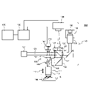
Fig. lA shows a first system 101 for microscopic analysis
of a sample S, in which the microscopic analysis path is
a confocal imaging path with scanning (point or line),
where the imaging may possibly be non-linear imaging.
The microscopic analysis system 101 comprises a
microscope objective 110 of given nominal numerical
aperture NA in a given field of view, a microscopic
analysis path 140, which is a scanning confocal imaging
path, and a sighting channel 150.
In this example, the microscopic analysis path 140
comprises an illumination path 120 configured to
illuminate the sample through the microscope objective
110 according to a given illumination pattern and in a
first spectral band, and a detection path 130 comprising
said microscope objective 110, said detection path being
configured to detect in the field of view, and according
to a given detection pattern, a light beam emitted by the
sample in response to said illumination of the sample.
The microscopic analysis path 140 also comprises a
processing unit 160 and a display module 170.
Date Regue/Date Received 2023-01-17
CA 03189741 2023-01-17
WO 2022/017784 - 15 -
PCT/EP2021/068661
In this example, the illumination path 120 of the
microscopic analysis path 140 comprises an illumination
source 121 and a cylindrical lens or deflection mirror
122 (optional). The illumination path also comprises a
splitter element 141 (splitter cube or splitter plate)
and a reflecting element 142 (optional) which are
configured to send an illumination beam, emitted by the
illumination source 121, toward the microscope objective
110, and also a device 143 for scanning the illumination
beam, configured to scan the illumination beam along one
or two dimensions. A splitter element 145 is configured
to separate the sighting path 150 and the microscopic
analysis path 140. The splitter element 145 is, for
example, a splitter cube or a splitter plate having a
reflection/transmission ratio of between 10/90 and 90/10;
it can be about 50/50. Moreover, a platform 111
(optional) rigidly connected to the microscope objective
110 permits an axial displacement 112 of the objective
with respect to the sample. The illumination source 121
can comprise, for example, a source of emission of
coherent (spatially), monochromatic and collimated
light. Optics and/or spatial filters (not shown) can make
the source collimated and/or coherent and/or
monochromatic. The wavelength of the source depends on
the application. For confocal microscopy using reflection
of the illumination beam off the sample, and applied to
imaging of the skin, a typical wavelength of the
illumination source is about 800 nm. For confocal
microscopy using fluorescence or nonlinear microscopy,
the wavelength can be adapted to the wavelength of
fluorescence excitation or of nonlinear emission of the
sample. Depending on the applications, a polychromatic
source can also be used. Moreover, in nonlinear
microscopy, for example in CARS or SRS microscopy, the
source 121 can comprise a plurality of distinct emission
sources (spatially coherent, monochromatic and
collimated), which are combined via a cube or a plate.
In the case of fluorescence/nonlinear microscopy, a
dichroic splitter element 141 will advantageously be used
Date Regue/Date Received 2023-01-17
CA 03189741 2023-01-17
WO 2022/017784 - 16 -
PCT/EP2021/068661
which reflects the excitation wavelength and transmits
the emission wavelength of the sample (or vice versa).
The cylindrical optical element 122 is optional and
permits microscopy with illumination along a line (so-
called "line-field" microscopy).
The illumination beam scanner 143 can be configured for
two-dimensional scanning in order to form an image from
the scanning of an illumination point. In the case of a
"line-field" system with a cylindrical lens or deflection
mirror 122, the illumination beam scanner 143 will be
able to be configured for one-dimensional scanning. The
scanning device can comprise one or more scanning
elements chosen from among the following elements:
galvanometric mirrors, polygonal mirrors, electrical or
acoustic-optical deflection systems, or a combination of
these various elements (in the case of bi-dimensional
scanning). The scanning device can also include optics
in order to conjugate at least one of said scanning
elements with an entrance pupil of the microscope
objective 110, for example in order to avoid vignetting.
In this example, the detection path 130 of the
microscopic analysis path 140 comprises a detector 138,
the microscope objective 110, the scanning device 143,
and the reflecting or partially reflecting elements 145,
142 (optional), 141 configured to send a beam, emitted
by the sample S in response to said illumination of the
sample, toward the detector 138. In this example, the
detection path 130 further comprises a lens 131
configured to optically conjugate, with the microscope
objective, a plane of the sample S with a detection area
of the detector 138. The lens 131 or "tube lens" can of
course be composed of several optical lenses and can also
be replaced by one or more reflecting elements, for
example a spherical or parabolic mirror.
The detector 138 comprises an optical sensor with a
detection area and can also include spatial filters for
confocal detection, if this is not ensured by the
detection area dimensions, and/or spectral filters to
limit the wavelength band detected to the emission band
Date Regue/Date Received 2023-01-17
CA 03189741 2023-01-17
WO 2022/017784 - 17 -
PCT/EP2021/068661
of the sample in the case of a fluorescence/nonlinear
microscopy system. The sensor can comprise an elementary
detection surface (e.g. a photodiode) in the case of a
point scanning system, a one-dimensional sensor (e.g. a
linear camera) in the case of a "line-field" system, or
a two-dimensional sensor of which only a region of
interest is considered in order to serve as an elementary
detection area or one-dimensional sensor. It will be
noted that a two-dimensional sensor can also be used in
a "conventional" way if a second scanning device similar
to device 143 is placed upstream of the sensor. The
processing unit 160 receives, in a known manner, a
detection signal generated by the detector 138 and
reconstructs microscopic images from the detection
signal, for example a 2D en-face image from a detection
signal resulting from scanning of a point or line
illumination pattern, for example.
The processing unit is connected to a display module 170
configured to represent a sighting image and, on the
sighting image, an image element indicating the position
of the detection pattern, as will be illustrated in more
detail below. The processing unit can also be connected
to a storage unit (not shown) for storing the images
and/or videos generated.
The microscopic analysis system 101 further comprises the
sighting path 150. As is illustrated in Fig. 1A, the
sighting path 150 comprises the microscope objective 110,
the beam splitter 145, a full-field illumination device
158 configured to illuminate the sample in a second
spectral band, a two-dimensional detector 155 with a
detection area 156, and one or more imaging elements
represented in Fig. lA by the elements 151, 152
configured to form, with said microscope objective 110,
a full-field imaging device which optically conjugates a
given effective field of the sample with the detection
area 156 of the two-dimensional detector 155. The
sighting path thus makes it possible to form a sighting
image in surface reflection of the effective field which,
Date Regue/Date Received 2023-01-17
CA 03189741 2023-01-17
WO 2022/017784 - 18 -
PCT/EP2021/068661
as will be described in more detail below, encompasses
the field of view of the microscope objective.
In this example, the full-field illumination device 158
comprises a plurality of light sources which are arranged
on a periphery of a distal face of the microscope
objective 110 and
allow direct illumination of the
sample S. The light sources are, for example, light-
emitting diodes emitting at wavelengths of between about
400 nm and about 800 nm. Of course, other illumination
devices are possible, for example a source arranged
upstream of the microscope objective and a beam splitter
element, for example a splitter cube, configured to
direct an illumination beam through the microscope
objective, toward the sample.
As is shown in Fig. 1A, the two-dimensional detector 155
is connected, in this example, to the processing unit 160
for the acquisition and display of the sighting image on
the display module 170.
In operation, the sighting path 150 thus makes it
possible to generate a sighting image in surface
reflection of the sample with a larger field than the
field of view of the microscope objective. Moreover, an
image element which indicates the position of the
detection pattern is shown on the sighting image, it
being possible for the detection pattern to be a point,
a line or a surface. It is thus possible for a user, for
example a practitioner, to precisely identify the field
of the microscopic analysis in the wide-field sighting
image.
Fig. 1B shows a second example of a system 102 for
microscopic analysis of a sample S, in which the
microscopic analysis path is an optical coherence
tomographic (OCT) microscopy path, for example a confocal
OCT channel, for example of the LC-OCT type as described,
for example, in [Ref. 4] or [Ref. 5].
As in the preceding example, the microscopic analysis
system 102 comprises a microscope objective 110 of given
nominal numerical aperture (NA) in a given field of view,
the microscopic analysis path 140, which is an optical
Date Regue/Date Received 2023-01-17
CA 03189741 2023-01-17
WO 2022/017784 - 19 -
PCT/EP2021/068661
coherence tomographic (OCT) path, the sighting channel
150, a processing unit 160, and a display module 170.
In this example, the sighting path 150 may be similar to
the sighting path described with reference to Fig. 1A,
only the microscopic analysis path 140 being different.
In the example of Fig. 1B, the microscopic analysis path
140 comprises an illumination path 120 configured to
illuminate the sample through the microscope objective
110 according to a given illumination pattern. In this
example, the illumination path comprises an illumination
source 121, a cylindrical lens or deflection mirror 122
(optional), a splitter element 141 (splitter cube or
splitter plate) and a reflecting element 142 (optional)
which are configured to send an illumination beam,
emitted by the illumination source 121, toward the
microscope objective 110. In this example, the
illumination path 120 also comprises a device 143 for
scanning the illuminating beam, configured to scan the
illumination beam along one or two dimensions, a splitter
element 145 configured to separate the sighting channel
150 and the microscopic analysis channel 140, and
(optionally) a platform 111 rigidly connected to the
microscope objective 110 and (for example) to the
splitter element 141, configured for an axial
displacement 112 of the objective with respect to the
sample.
The illumination source 121 can comprise, for example, a
source of emission of coherent (spatially),
polychromatic, collimated light. Optics and/or spatial
filters (not shown) can make the source collimated and/or
coherent and/or with a specific spectral distribution.
The central wavelength of the source depends on the
application, for example of between 600 nm and 1500 nm,
and the spectral width for example between 50 nm and
about 250 nm. In the case of an LC-OCT application as
described for example in Ref. 4, the illumination source
121 can comprise, for example, and in a non-limiting way,
a supercontinuum laser spectrally filtered by an optical
fiber for an emission of about 800 nm and collimated by
Date Regue/Date Received 2023-01-17
CA 03189741 2023-01-17
WO 2022/017784 - 20 -
PCT/EP2021/068661
an off-axis parabolic mirror. In the case of an
application to full-field tomographic imaging or FF-OCT
(full-field OCT), as described for example in the article
by E. Beaurepaire et al. [Ref. 11], the illumination
source 121 can be chosen to be spatially non-coherent and
to comprise means for full-field illumination of the
sample, for example a Kohler illumination system. The
cylindrical optical element 122 is optional and permits
microscopy with illumination along a line (line-field
microscopy).
The scanning device 143 for the illumination beam can be
configured for one-dimensional or two-dimensional
scanning of a point or a line in order to form, in a
known manner, a cross-sectional image of the so-called
B-scan sample, that is to say in a plane parallel to the
optical axis of the microscope objective, a cross-
sectional image of the sample called a C-scan, or en-
face image, that is to say in a plane perpendicular to
the optical axis of the microscope objective, or a 3D
image of the sample resulting from the acquisition of a
plurality of B-scan images or C-scan images. As before,
the scanning device can comprise one or more scanning
elements selected from among the following elements:
galvanometric mirrors, polygonal mirrors, electrical or
acousto-optical deflection systems, or a combination of
these different elements (in the case of two-dimensional
scanning). The scanning device can also include optics
for conjugating at least one of said scanning elements
with an entrance pupil of the microscope objective 110,
for example in order to avoid vignetting.
The detection path 130 of the microscopic analysis path
is configured to detect a light beam emitted by the sample
in response to said illumination of the sample, according
to a given detection pattern, but differs from the
detection path of the microscopic analysis path
illustrated in Fig. 1A. In particular, the detection path
comprises an interferometer for implementation of optical
coherence tomographic microscopy. More precisely, the
interferometer comprises an object arm with the
Date Regue/Date Received 2023-01-17
CA 03189741 2023-01-17
WO 2022/017784 - 21 -
PCT/EP2021/068661
microscope objective 110, the scanning device 143 and the
reflecting or partially reflecting elements 145, 142,
141, which are configured to send a beam, emitted by the
sample S in response to said illumination of the sample,
toward a detector 138.
The interferometer of the detection path further
comprises a reference arm, separated in this example from
the object arm by the splitter cube 141, and comprising
in a known manner a microscope objective 133 (optional),
for example similar to the microscope objective 110 in
order to provide dispersion compensation, a dispersion
compensation system (optional, not shown in Fig. 1B,
especially in the case where there is no microscope
objective 133), a reference mirror 135, a platform 134
(optional) configured for example to cause the reference
mirror 135 to move when a modulation of the optical path
on the reference arm is required. In this example, the
detection path further comprises an objective 131
configured to optically conjugate, with the microscope
objective, a plane of the sample S with a detection area
of the detector 138.
As in the preceding example, the detector 138 comprises
an optical sensor with a detection area, and it can also
include spatial filters for confocal detection, if this
is not ensured by the dimensions of the detection area,
and/or spectral filters in order to limit the detected
wavelength band. The sensor can comprise an elementary
detection surface (e.g. a photodiode) in the case of a
point scanning system, a one-dimensional sensor (e.g. a
linear camera) in the case of a line-field system, or a
two-dimensional sensor of which only a region of interest
is considered in order to serve as an elementary
detection area or as a one-dimensional sensor. In the
case of an FF-OCT application, a two-dimensional sensor
can be used conventionally.
In operation, interferences are created at the detection
area of the detector 138 between the light coming from
the reference arm and the light backscattered by the
sample illuminated according to the illumination pattern,
Date Regue/Date Received 2023-01-17
CA 03189741 2023-01-17
WO 2022/017784 - 22 -
PCT/EP2021/068661
optionally and in a known manner with a modulation of the
path length difference between the reference arm and the
object arm of the sample, for the formation of
tomographic images, in particular en-face images. The
processing unit 160 receives, in a known manner,
detection signals generated by the detector 138 and
resulting from the detection of interferences, and it is
configured for the reconstitution of microscopic images
from the detection signals, for example images in 2D
section (B-scan or C-scan). The processing unit 160 is
connected to a display module 170 configured to represent
the sighting image and, on the sighting image, an image
element indicating the position of the detection pattern,
as will be illustrated in more detail below. The
processing unit can also be connected to a storage unit
(not shown) for storing the images and/or videos
generated.
Such a microscopic analysis path 140 thus functions as a
known optical coherence tomographic microscopy channel
from the prior art. Although a particular example is
shown in Fig. 1B, a person skilled in the art will
understand that the microscopic analysis system according
to the present description applies to any assembly known
from the prior art for optical coherence tomographic
microscopy, and the optomechanical elements shown in Fig.
1B can be adapted accordingly.
According to exemplary embodiments, in the case of a
microscopic analysis path suitable for the formation of
vertical cross-sectional images of the sample (B-scan)
by scanning a line in depth, the formation of B-scan
images will be able to be synchronized with a rate of
acquisition of the sighting images. Indeed, when the
acquisition of B-scan images comprises scanning of the
illumination beam in depth in the sample by means of a
displacement of the microscope objective for example, the
synchronization makes it possible to ensure that the
sighting images are acquired with an identical position
of the microscope objective with reference to the surface
of the sample.
Date Regue/Date Received 2023-01-17
CA 03189741 2023-01-17
WO 2022/017784 - 23 -
PCT/EP2021/068661
Fig. 10 shows a third example of a system 103 for
microscopic analysis of a sample S, in which the
microscopic analysis path is a spectroscopy path, for
example Raman spectroscopy.
As in the preceding examples, the microscopic analysis
system 103 comprises a microscope objective 110 of given
nominal numerical aperture NA in a given field of view,
the microscopic analysis path 140, which is a
spectroscopy path, and the sighting path 150.
In this example, sighting path 150 may be similar to the
sighting path described with reference to Fig. 1A, only
the microscopic analysis path 140 being different.
The microscopic analysis path 140 comprises an
illumination path 120 comprising, in this example, an
illumination source 121, a cylindrical lens or deflection
mirror 122 (optional), a splitter element 141 (splitter
cube or splitter plate) and a reflecting element 142
(optional), which are configured to send an illumination
beam, emitted by the illumination source 121, toward the
microscope objective 110. In this example, the
illumination path 120 also comprises a scanning device
143 (optional) for the illumination beam, configured to
scan the illumination beam along one or two dimensions,
a splitter element 145 configured to separate the
sighting path 150 and the microscopic analysis path 140,
and (optionally) a platform 111 rigidly connected to the
microscope objective 110 and configured for axial
displacement 112 of the objective with respect to the
sample.
The illumination source 121 can comprise, for example, a
source of coherent (spatially), monochromatic and
collimated light. A polychromatic source can also be
used, for example in diffuse reflection micro-
spectroscopy. Optics and/or spatial filters (not shown)
can make the source collimated and/or coherent and/or
monochromatic. The wavelength of the source depends on
the application. In Raman microspectroscopy for example,
applied to imaging of the skin, a typical wavelength of
Date Regue/Date Received 2023-01-17
CA 03189741 2023-01-17
WO 2022/017784 - 24 -
PCT/EP2021/068661
the illumination source can be between about 780 nm and
about 830 nm.
The cylindrical optical element 122 is optional and
permits microscopy with illumination along a line (line-
field).
The detection path 130 of the microscopic analysis path
is configured to detect a light beam emitted by the sample
in response to said illumination of the sample, according
to a given detection pattern, but differs from the
detection path of the microscopic analysis path
illustrated in Fig. 1A or in Fig. 1B. In particular, the
detection path comprises, in addition to the microscope
objective 110, the scanning device 143 (optional) and
reflecting or partially reflecting elements 145, 142,
141, a spectrometer. The spectrometer comprises, in this
example and in a known manner, a spectral dispersion
element 132, for example a grating, an objective 133, and
a detector 134, comprising a sensor with a one-
dimensional or two-dimensional detection area. A two-
dimensional sensor makes it possible, in a line-field
configuration, to measure a spectrum for each point of
the detection pattern (measurement of several spectra in
parallel, each line of the 2D sensor thus corresponding
to the spectrum of a point in the detection pattern).
The processing unit 160 receives, in a known manner,
detection signals generated by the detector 134 of the
spectrometer for the reconstruction of spectroscopic
signals at one or more points of the sample. The
processing unit 160 is connected to a display module 170
configured to represent the sighting image and, on the
sighting image, an image element indicating the position
of the detection pattern, as will be illustrated in more
detail below. The processing unit can also be connected
to a storage unit (not shown) for storing the images
and/or videos generated.
Such a microscopic analysis path 140 therefore functions
as a spectroscopy path known from the prior art. Although
a particular example is shown in Fig. 1C, a person skilled
in the art will understand that the microscopic analysis
Date Regue/Date Received 2023-01-17
CA 03189741 2023-01-17
WO 2022/017784 - 25 -
PCT/EP2021/068661
system according to the present description applies to
any assembly known from the prior art for spectroscopy,
and in particular Raman spectroscopy, and the
optomechanical elements represented in Fig. 10 can be
adapted accordingly.
As before, in operation, the sighting path 150 makes it
possible to generate a sighting image in surface
reflection of the sample S with a larger field than the
field of view of the microscope objective. Moreover, an
image element which indicates the position of the
detection pattern of the microscopic analysis path is
represented on the sighting image, it being possible for
the detection pattern to be a point, a line or a surface.
It is thus possible for a user, for example a
practitioner, to precisely identify the field of the
microscopic analysis in the wide-field sighting image.
In each of the examples illustrated in Figures 1A, 1B or
1C, the splitter element 145 configured to separate the
sighting path 150 and the microscopic analysis path 140
is arranged to transmit a beam, emitted by the sample in
response to said illumination of the sample by the
illumination device 158 of the sighting path, toward the
two-dimensional detector 155 and to reflect a beam,
emitted by the sample in response to said illumination
of the sample by the illumination path 120 of the
microscopic analysis path, toward the detection path 140.
Of course, it would be possible to make the splitter
element 145 work in reflection on the sighting path and
in transmission on the microscopic analysis path.
Moreover, when the microscopic analysis path comprises a
scanning device (143, Figures 1A-1C), the beam splitter
element may form part of the scanning device.
Whether in one or other of the configurations, the
splitter element can be configured to limit the light
power in the sighting path 150 of the light coming from
the illumination path 120 of the microscopic analysis
path and reflected by the sample. Indeed, the light, for
example coming from a laser source, can be powerful and
likely to cause glare in the sighting path. Thus, it is
Date Regue/Date Received 2023-01-17
CA 03189741 2023-01-17
WO 2022/017784 ¨ 26 ¨
PCT/EP2021/068661
possible to use a splitter element with a reflection
coefficient different from the transmission coefficient
(for example a glass slide). To reduce the light power
in the sighting path, it is also possible to add an
optical density in the sighting path 150 (downstream of
the splitter element 145).
In the case where the spectral band of the illumination
source 121 of the illumination path 120 of the
microscopic analysis path is at least partially different
from the spectral band of the illumination device 158 of
the sighting path, it will be possible for the splitter
element to further comprise a dichroic element, for
example a plate or a dichroic cube.
It is also possible to provide means for reducing the
light power in the sighting path, these means for
reducing the light power possibly containing a spectral
filtering element when the spectral band of the
illumination source 121 of the illumination path 120 of
the microscopic analysis path is at least partially
different from the spectral band of the illumination
device 158 of the sighting path.
It is also possible not to activate the illumination of
the sighting and microscopic analysis paths continuously,
in the event that illumination of one of the paths could
interfere with detection on the other path.
Thus, in practice, the microscopic analysis of the sample
and the formation of a sighting image can be carried out
continuously. This is the case when the image element is
directly the image, formed by the wide-field imaging
device of the sighting path, of the illumination pattern
of the microscopic analysis path. This may also be the
case when the image element is a graphic element
indicating the position of the detection pattern and when
the illumination of the microscopic analysis path does
not interfere with the detection of the sighting path,
for example because it is greatly attenuated in the
sighting path, and reciprocally.
In other exemplary embodiments, the method can comprise
a first step of formation of a sighting image of the
Date Regue/Date Received 2023-01-17
CA 03189741 2023-01-17
WO 2022/017784 - 27 -
PCT/EP2021/068661
sample with the illumination of the microscopic analysis
path turned off, the detection of an analysis zone of
interest in the sighting image of the sample, then the
microscopic analysis of the sample in said zone of
interest, for example by moving the sample in order to
bring the graphic element, previously calibrated to
indicate the detection zone, to the level of the analysis
zone of interest.
This configuration is of interest in the case where the
illumination of the microscopic analysis path may
interfere with detection in the sighting path.
In some cases, the sighting channel can operate
continuously, both for illumination and for acquisition,
if the illumination of the sighting path does not
interfere with the detection of the microscopic analysis
path. This makes it possible to have a continuous
sighting image, even if it is degraded during the time
when the illumination of the microscopic analysis path
is activated.
In other cases, the illumination of the sighting path can
be turned off during the microscopic analysis of the
sample, for example when the illumination of one path
interferes with the detection on the other path and it
is not possible to simultaneously maintain the
illumination on both paths in order to obtain usable
results.
Fig. 2 shows a diagram which illustrates an example of a
sighting path of a system for microscopic analysis of a
sample according to the present description. The sighting
path shown in Fig. 2 is in particular configured to
operate with any of the systems shown as examples in
Figures 1A, 1B or 10. In Fig. 2, only the detection part
of the sighting path is shown, the illumination possibly
comprising, as illustrated in Figures lA to 1C, a set of
light sources arranged on the distal part of the
microscope objective, or any other device for full-field
illumination of the sample S.
As is illustrated in Fig. 2, the sighting path comprises
the microscope objective 110, of which the exit pupil is
Date Regue/Date Received 2023-01-17
CA 03189741 2023-01-17
WO 2022/017784 ¨ 28 ¨
PCT/EP2021/068661
indicated by reference sign 115, and a two-dimensional
detector, represented in Fig. 2 by a detection area 156,
and an objective 253.
In this example, the sighting path further comprises a
tube lens 251 and an eyepiece 252. These imaging elements
form, together with the objective 253 and the microscope
objective 110, a full-field imaging device 250 configured
to optically conjugate a given effective field of the
sample encompassing said field of view with the area of
detection 156 of the two-dimensional detector.
Thus, unlike certain systems known from the prior art and
in particular [Ref. 8], which describes a micro-camera
integrated in the object space of the microscope
objective, the sighting path according to the present
description, by virtue of being moved apart from the
object space, makes it possible to form a sighting image
in surface reflection of a field of the sample, called
the effective field in the present description, which
includes the field of view of the microscope objective,
the sighting image being able to have a very good optical
quality without affecting the object space of the
objective. The dimensions of the effective field are
limited by the full-field imaging device of the sighting
path. The effective field can be defined by a circle with
a diameter of between about 2 mm and about 5 mm.
To further improve the optical quality of the sighting
image, it is advantageous for the full-field imaging
device to have a numerical aperture, measured in the
object space of the microscope objective, strictly lower
than the nominal numerical aperture of the microscope
objective.
Indeed, in a conventional microscopic analysis path, it
is known to use a microscope objective with a high
numerical aperture (NA), for example an NA of between
about 0.5 and about 1.25. This numerical aperture is
guaranteed by the manufacturer for a nominal field,
called the field of view in the present description,
which can be between about 500 pm and about 1.5 mm.
Date Regue/Date Received 2023-01-17
CA 03189741 2023-01-17
WO 2022/017784 - 29 -
PCT/EP2021/068661
However, because the microscope objective 110 is not used
in the sighting path under nominal conditions of use, the
resolution accessible at the level of the sighting path
may differ from the one announced in the specifications
of the objective. In particular, by using the microscope
objective with an effective field greater than the
nominal field of view, aberrations and/or vignetting may
adversely affect the quality of the image. In order to
obtain a better image quality for the sighting path, it
is therefore possible to design a full-field imaging
device which has a numerical aperture strictly lower than
the nominal numerical aperture of the microscope
objective, for example a numerical aperture of between
about 0.05 and 0.1.
An originality of the microscopic analysis system
according to the present description is thus to be able
to use the same microscope objective in two different
optical paths, with possibly different numerical
apertures: in the microscopic analysis path in which the
microscope objective is used under nominal conditions
(high numerical aperture, high resolution and low field),
and in the sighting path in which the microscope
objective is combined with other optical elements to form
a full-field imaging device which optionally has a lower
numerical aperture, for example about 0.08, a lower
resolution and a wide field. The microscopic analysis
system according to the present description can thus be
seen as two microscopes operating in parallel via a
single microscope objective.
In practice, the numerical aperture of the full-field
imaging device 250 of the sighting path can be limited
by placing a diaphragm 255 in the sighting path, for
example in a plane substantially conjugate with a plane
of the exit pupil 115 of the microscope objective.
Figures 3A and 3B thus illustrate two examples for the
reduction of the numerical aperture of the full-field
imaging device 250. In these examples, the microscope
objective 110 is not shown.
Date Regue/Date Received 2023-01-17
CA 03189741 2023-01-17
WO 2022/017784 - 30 -
PCT/EP2021/068661
Fig. 3A shows a diagram illustrating a first example in
which the sighting path comprises a diaphragm 255 making
it possible to limit the numerical aperture of the full-
field imaging device.
Fig. 3B shows a diagram illustrating a second example in
which the numerical aperture of the full-field imaging
device 250 of the sighting path is limited by one of the
optical elements of the full-field imaging device, in
this example the objective 253 of the camera. This
configuration is particularly of interest because it
makes it possible to reduce the size of the full-field
imaging device 250 and thus to obtain a very compact
sighting path. Of course, the numerical aperture of the
full-field imaging device 250 of the sighting path could
be limited by another of the optical elements of the
full-field imaging device, for example the eyepiece 252.
It will be noted that it is not essential for the
diaphragm (255 in Fig. 3A or 253 in Fig. 3B) to be
perfectly conjugate with the plane of the pupil of the
microscope objective. However, if the plane of the
diaphragm is substantially conjugate with the plane of
the exit pupil of the microscope objective (as is shown
for example in Fig. 2), this makes it possible not to
lose the property of telecentricity of the microscope
objective and to prevent rays from being vignetted within
the microscope objective 110.
Moreover, the full-field imaging device 250 illustrates
an example of the design of the sighting path, but other
examples are possible. For example, the full-field
imaging device 250 of the sighting path might not
comprise an eyepiece 252, the camera objective 253
imaging a finite distance, or the eyepiece 252 might not
return the rays to infinity. In any case, as has been
explained above, it is advantageous to reduce the
numerical aperture (NA) of the device 250, in the object
space of the microscope objective, compared to the
nominal NA of the microscope objective, whether by means
of a diaphragm added in the sighting path or by means of
Date Regue/Date Received 2023-01-17
CA 03189741 2023-01-17
WO 2022/017784 - 31 -
PCT/EP2021/068661
one of the optical elements of the sighting path
configured to form a diaphragm.
Moreover, the full-field imaging device of the sighting
path can also be adjustable in focus. This makes it
possible to form a sighting image in surface reflection
of the sample even when the microscopic analysis path is
configured to form an image deep in the sample (case of
OCM imaging as illustrated in Fig. 1B for example).
Indeed, when the microscopic analysis path is an LC-OCT
path for example, the microscope objective 110 is caused
to be translated vertically, that is to say along its
optical axis. The translation can be dynamic in a mode
of vertical scanning of the illumination line (obtaining
B-scans), that is to say in a direction parallel to the
optical axis of the microscope objective, or controlled
by the user in a mode of horizontal scanning of the
illumination line, that is to say in a direction
contained in a plane perpendicular to the optical axis
of the microscope objective (obtaining C-scans). In the
sighting path, however, it is desired that the microscope
objective continues to image the surface of the sample,
for example the surface of the skin, which remains at the
same position when the microscope objective is
translated. In order to maintain optimal image quality
for the sighting image, it may therefore be useful to be
able to modify the focusing of the wide-field imaging
device 250 of the sighting path in order to maintain an
optical conjugation between the surface of the sample S
and the detection area 156 (Fig. 2).
To do this, it is possible to provide for one of the
optical elements, for example the objective 253, a lens
with variable focal length, or to provide that this
objective can be moved, for example using a piezoelectric
motor, the detection area being held fixed. In practice,
the adjustment of the focusing can be automatic
(autofocus), which makes it possible to limit the
adjustments that have to be made by the user. However,
when the sample is the skin for example, there are not
always enough clear structures to allow the autofocus to
Date Regue/Date Received 2023-01-17
CA 03189741 2023-01-17
WO 2022/017784 - 32 -
PCT/EP2021/068661
be performed in an effective way. Another possibility is
then to calibrate the adjustable focusing of the wide-
field imaging device 250 of the sighting path in such a
way as to associate the correct focusing position with
each position of the microscope objective within its
travel.
Fig. 4 shows, by way of illustration, various examples
showing the field of view 401 of the microscope objective
110, for which a nominal numerical aperture is guaranteed
by the manufacturer, the effective field 402 of the
sighting path, and a total field 403 of the microscope
objective. The total field of the microscope objective
is a region of a focal plane of the microscope objective
comprising all the points from which a light ray can be
collected by the objective. In practice, the effective
field 402 is chosen to be large enough to obtain a wide-
field sighting image, but smaller than the total field
in order to keep a sighting image of sufficient optical
quality.
On these three examples are shown three detection
patterns of the microscopic analysis path, namely a line
431, a surface 432, and a point 433. In all cases, the
detection pattern is included in the field of view of the
microscope objective.
A method for microscopic analysis according to the
present description can be implemented by means of a
microscopic analysis system as described, for example and
in a nonlimiting manner by means of one of the systems
101, 102, 103 described with reference to Figures 1A, 1B
and 1C respectively.
The method comprises the microscopic analysis of the
sample S, for example a biological tissue such as skin,
by means of a microscopic analysis path 140 as described
for example with reference to Figures 1A, 1B or 1C, and
the formation of a sighting image of the sample by means
of a sighting path 150 as described for example with
reference to Figures 1A-1C and Figures 2 and 3A-3B above.
The sighting image is a reflection image of an effective
Date Regue/Date Received 2023-01-17
CA 03189741 2023-01-17
WO 2022/017784 - 33 -
PCT/EP2021/068661
field 402 (Fig. 4) of the sample comprising the field of
view 401, as has been explained above.
The method for microscopic analysis according to the
present description further comprises the display, on the
sighting image, of an image element indicating the
position of the detection pattern (for example a
detection pattern 431, 432 or 433 as shown in Fig. 4).
In exemplary embodiments of a method according to the
present description, the image element can be directly
the image formed, by the wide-field imaging device of the
sighting path, of the illumination pattern formed on the
sample by the illumination path 120 of the microscopic
analysis path 140 (see Figures 1A, 1B and 1C).
However, in certain exemplary embodiments, the image
element can be a graphic element indicating the position
of the detection pattern and determined by means of a
prior calibration step.
This configuration is particularly advantageous
especially when the illumination pattern is not detected
by the detector of the sighting path, for example either
because the detector of the sighting path is not
sensitive in the spectral band of the illumination source
of the microscopic analysis path, or because the first
spectral band is cut in the sighting path in order to
limit glare. This configuration is also advantageous when
the illumination pattern is difficult to identify in the
sighting image, or if the detection pattern is
substantially different from the illumination pattern.
Fig. 5A thus shows diagrams illustrating, according to a
first exemplary embodiment applied to microscopic
imaging, calibration steps for determining, for said
image element, a graphic element indicating the position
of the detection pattern of the microscopic imaging path,
in this example a detection pattern formed of a
rectangular surface. The calibration method is
implemented with a calibration sample which has a sharp
edge, for example the edge of a glass slide cut "at right
angles", or the edge of a pattern printed by
photolithography on a glass slide.
Date Regue/Date Received 2023-01-17
CA 03189741 2023-01-17
WO 2022/017784 - 34 -
PCT/EP2021/068661
A first step 501 involves acquisition of a sighting image
510 of the calibration sample and a microscopic en-face
image 520 such that a sharp edge of the sample visible
on the sighting image is visible on an edge of the
microscopic image 520, in this example a right edge. The
line 531 of the sighting image is then recorded as being
the right edge of the detection area of the microscopic
analysis path. The method is repeated in a second step
502 by moving the sample so that this time the sharp edge
of the sample is situated on another side of the
microscopic image, in this example the left edge. In the
same way, the image 532 of the sighting image is recorded
as being the left edge of the detection area of the
microscopic analysis path. The method is repeated in
steps 503, 504 in the same way, each time moving the
sample in order to make the sharp edge appear on a new
side of the microscopic image 520. A corresponding line
534, 535 is recorded each time on the sighting image. As
is illustrated in diagram 505, starting from the 4 lines
recorded on the sighting image, it is possible to
reconstruct a graphic element which indicates the
position of the detection pattern, in this example a
rectangular surface which can be materialized by a
rectangle on the sighting image during the acquisition
of a microscopic image. The calibration thus makes it
possible to perfectly identify the detection pattern of
the microscopic analysis path in the sighting path, and
this independently of the sample that is analyzed. The
calibration can be adapted to a line or point detection
pattern.
Fig. 5B shows diagrams illustrating, according to a
second example applied to spectroscopic analysis, for
example Raman spectroscopic analysis, calibration steps
for determining, for said image element, a graphic
element indicating the position of the detection pattern,
in this example a detection point.
In a first step 541, a sighting image 510 of the
calibration sample is acquired, and a Raman signal (561)
is measured at the same time.
Date Regue/Date Received 2023-01-17
CA 03189741 2023-01-17
WO 2022/017784 ¨ 35 ¨
PCT/EP2021/068661
The reference sample is moved, for example from left to
right, until a strong Raman signal (562) is observed.
This corresponds to a first sharp edge of the calibration
sample 551 that is recorded. The method is repeated in a
second step 542 by moving the calibration sample, for
example from bottom to top, until again a strong Raman
signal appears (spectrum 562). This corresponds to a
second sharp edge of the calibration sample 552 that is
recorded. As is illustrated in step 543, starting from
the two straight lines 551, 552 recorded, it is possible
to determine a graphic element representative of the
detection pattern 530 (here a disk centered on the
detection point) and positioned at the intersection of
the two straight lines. It is possible to ensure the
precision of the calibration by repeating the steps 541,
542 but by going, for example, from right to left and
then from top to bottom. The calibration thus makes it
possible to perfectly identify the detection pattern of
the microscopic analysis path in the sighting path, and
this independently of the sample analyzed.
In practice, a method for the microscopic analysis of a
sample, for example the analysis of the skin of a patient,
can be carried out in the following way by a practitioner,
for example a dermatologist, by implementing the steps
of a method according to the present description.
In a first step, a visual examination of the skin is
carried out. Clinical images (photos) can be taken in
order to locate "suspect" structures on a body scale. A
dermoscopic examination follows. The dermatologist takes
images of the suspect structure using a magnifying
optical system, for example a dermatoscope, which
optically corresponds to a magnifying glass, either
digital or non-digital, with integrated illumination. The
field of view of the deimatoscope is typically 1 to 3 cm.
Dermoscopic images can be recorded directly with a
digital dermatoscope or with the aid of a camera.
If any doubt persists during the dermoscopic examination,
the dermatologist proceeds to a microscopic analysis of
the skin, for example by means of a system as illustrated
Date Regue/Date Received 2023-01-17
CA 03189741 2023-01-17
WO 2022/017784 - 36 -
PCT/EP2021/068661
in Fig. 1B, for example with a microscopic analysis path
of the LC-OCT type. The dermatologist positions the
manual probe head (that is to say the part of the system
in contact with the skin for imaging) as close as possible
to the suspect structure. He then moves the whole probe
(while keeping it in contact with the skin) until he
precisely locates the lesion previously identified in
dermoscopy, being guided by the sighting path.
Once the structure is identified on the sighting image,
the dermatologist proceeds to analyze the skin at the
cellular level and in depth by virtue of the LC-OCT
microscopic analysis path.
The examination begins, for example, with the vertical
section imaging mode (B-scan), which gives access
directly to the entire depth of the structure. By virtue
of the image element displayed on the macro image
indicating the position of the detection pattern (a line
in the case of the cross-sectional imaging mode), the
practitioner knows perfectly at what level in the
structure he is in the process of observing a vertical
section at the cellular scale.
The dermatologist may also be interested in the LC-OCT
image in order to search for pathological markers at the
cellular level/deep within the skin, in order to enrich
the information already obtained by dermoscopy. At this
stage, it is possible to move around in the structure in
order to look for these pathological markers or to study
them.
This movement can be done in two ways. Laterally by virtue
of the scanning device (143 in Fig. 1B) present in the
device, which makes it possible to scan the detection
pattern. The amplitude of this scan is quite low (-500
pm), and in only one direction. The second way is to move
the whole probe or the skin under the probe. This
displacement will a priori be less fine (its precision
will depend on the control that the user is able to
exercise), but the dermatologist will have as much
amplitude as he wishes to target any zone in LC-OCT. For
this type of movement, the sighting image is important
Date Regue/Date Received 2023-01-17
CA 03189741 2023-01-17
WO 2022/017784 - 37 -
PCT/EP2021/068661
because it allows the dermatologist to ensure that he
always remains at the level of the structure during his
action in moving the probe or the skin.
Once the markers have been identified by LC-OCT, several
options are possible. The dermatologist can switch to
horizontal section mode (C-scan or en-face) in order to
enrich his understanding of the structure (with the same
approach to navigating the structure as in vertical
section mode).
It is also possible to acquire information within a
volume of the sample in order to study pathological
markers in 3D in a zone of interest. Following the
acquisition of one or more volumes, the dermatologist can
stop the acquisition system and study the volumes
acquired for analysis. It should be noted that the
recording of a volume is accompanied by the recording of
a certain number of sighting images acquired during the
3D acquisition (similarly, the recording of any
image/video is accompanied by the recording of the
associated sighting image/video). Several sighting
images are recorded during a 3D acquisition in the case
where the practitioner has moved during the acquisition
(3D acquisitions can be relatively long).
Figures 6A, 6B and 7 show images illustrating examples
of sighting images and microscopic B-scan and C-scan
images recorded during an acquisition of a volume by
means of a method according to the present description.
In these examples, the microscopic analysis path is an
LC-OCT type analysis path, as shown for example in Fig.
1B, configured for acquisition of 3D images. To obtain
these images, the source used (121 in Fig. 1B) is a
supercontinuum laser filtered by an optical fiber for an
emission at about 800 nm and collimated by an off-axis
parabolic mirror. The microscope objective 110 is an
objective immersed in silicone oil with 20x magnification
and a numerical aperture NA-0.5. A cylindrical lens 122
with a focal length of 50 mm permits illumination along
a line of -1.5 mm x 1.5 lam at skin level, with a power
of -10 mW. A galvanometric scanner (143 in Fig. 1B) is
Date Regue/Date Received 2023-01-17
CA 03189741 2023-01-17
WO 2022/017784 - 38 -
PCT/EP2021/068661
used for lateral scanning of the illumination line. The
fold mirror 142 is mounted on a piezoelectric actuator
for the modulation of the interferences for the
generation of the C-scan images. A microscope objective
133 identical to objective 110 is used in the reference
arm for dispersion compensation. The reference surface
135 of the interferometer is an air/glass interface of a
glass slide made of fused silica. The tube lens 131 has
a focal length of 150 mm, and detector 138 comprises a
CMOS line-scan camera. A 90:10 splitter plate (145) is
mounted on the scanning device 143 in order to separate
the microscope and sighting paths. The sighting path 150
comprises a camera 155 equipped with miniature optics of
a few mm, serving as a diaphragm, as described in Fig.
3B. The camera is equipped with focus/autofocus
adjustment.
Figures 6A and 6B thus illustrate, by way of example, a
B-scan image 620 displayed with a sighting image 610. On
the sighting image 610, the graphic element 630 indicates
the position of the detection pattern (line) of the
microscopic analysis path. The graphic element is
determined by virtue of a prior calibration, as described
for example with reference to Fig. 5A.
A marker 640 can further be superimposed on the sighting
image 610 in order to mark a point on the graphic element,
or more generally on the image element, so as to allow a
user to target a point in the B-scan image 620 and to
visualize the position of the point thus targeted at the
level of the surface of the sample on the sighting image.
For example, the targeted point in the image 620 is
indicated by a reticle 641. The marker is calibrated to
position itself at the level corresponding to the
position of the targeted point via the reticle, projected
onto the surface of the sample. Similarly, it is possible
to leave the possibility to the user of targeting a point
in the sighting image, within the detection pattern,
directly via the marker 640, so as to visualize to which
position corresponds a point of the detection pattern
Date Regue/Date Received 2023-01-17
CA 03189741 2023-01-17
WO 2022/017784 - 39 -
PCT/EP2021/068661
within the B-scan image (marked in this case by the
vertical axis of the reticle).
Fig. 6B illustrates the same image with movement of the
marker 640 and of the reticle 641, the user being able
either to move the reticle 641 so as to see the marker
reposition itself on the sighting image 610, or to move
the marker 640 so as to see the reticle reposition itself
on the B-Scan image 620.
Fig. 7 shows two images extracted from a volume, namely
a B-scan image 721 and a C-scan image 722. The sighting
image 710 is displayed at the same time with a detection
pattern 730 corresponding to a detection surface of the
C-scan.
Just as in the case of the B-scan image (Fig. 6A and Fig.
6B), a marker 740 can be superimposed on the graphic
element of the sighting image, or more generally on the
image element. The marker is calibrated so as to be able
to associate a point of the volume, marked here by a
reticle 741, with a point of the detection pattern marked
by the marker, at the level of the surface of the sample.
The user can then target a point via the marker 740,
respectively via the reticle 741, so as to visualize to
which position corresponds a point of the volume
projected onto the surface of the sample, within the
detection pattern, respectively to which position
corresponds a point of the detection pattern within the
volume, marked in this case by the axes of the reticle
that can be viewed in the C-scan images extracted from
the volume.
As is illustrated in these images, the method according
to the present description allows the practitioner to
precisely identify the field of the microscopic analysis
(in this example B-scans and C-scans) in the sighting
image, which has an image quality close to the quality
of a dermoscopic image.
Although described through a number of exemplary
embodiments, the method and the system for microscopic
analysis according to the present description include
variants, modifications and improvements which will be
Date Regue/Date Received 2023-01-17
CA 03189741 2023-01-17
WO 2022/017784 ¨ 40 ¨
PCT/EP2021/068661
obvious to a person skilled in the art, it being
understood that these variants, modifications and
improvements form part of the scope of the invention as
defined by the claims that follow.
Date Regue/Date Received 2023-01-17
CA 03189741 2023-01-17
WO 2022/017784 - 41 -
PCT/EP2021/068661
References
Ref. 1: M. Rajadhyaksha et a!, "In vivo confocal scanning laser microscopy of
human skin II: Advances in instrumentation and comparison with histology", J
Invest Dermatol, 1999.
Ref 2: K. K6nig et al, "High-resolution multiphoton tomography of
human skin with subcellular spatial resolution and picosecond time
resolution," J.
Biomed. Opt. 8, 432-439 (2003).
Ref. 3: Schmitt et al., "Subsurface Imaging of Living Skin with Optical
Coherence
Microscopy", Dermatology 1995;191:93-98.
Ref. 4: Published patent application W02015092019.
Ref. 5: Y. Chen et al. "High-resolution line-scanning optical coherence
microscopy", Optics Letters, vol. 32, no. 14, 1971-1973 (2007).
Ref. 6: J. Schleusener et al., "Raman spectroscopy for the discrimination of
cancerous and normal skin", Photon Lasers Med (2015).
Ref. 7: E. Drakaki et al. "Spectroscopic methods for the photodiagnosis of
nonmelanoma skin cancer", Journal of Biomedical Optics 18(6), 061221 (June
2013).
Ref. 8: Published patent application W02017139712.
Ref. 9: Granted patent U57864996.
Ref. 10: Z. Wu et al. "Precise in vivo tissue micro-Raman spectroscopy with
simultaneous reflectance confocal microscopy monitoring using a single laser",
vol. 44, no. 6 /15 March 2019 /Optics Letters.
Ref. 11: E. Beaurepaire et al. "Full-field optical coherence microscopy" Opt.
Lett.
23, 244-246 (1998)
Date Recue/Date Received 2023-01-17