Note: Descriptions are shown in the official language in which they were submitted.
CA 03189846 2023-01-23
STORAGE AND TRANSDUCTION OF QUANTUM INFORMATION
[0001]
Field
[0002] The present technology relates to the storage and manipulation of
quantum
information. Some embodiments provide methods and apparatus for transducing
quantum information between qubits having quantum states separated by
different
energies. For example, an application of the present technology is to
transduce
quantum information from qubits having energy level separations corresponding
to
microwave wavelengths to optical photons. Another application of the present
technology is to store quantum information. Another application of the present
invention is to create quantum entanglement among plural qubits.
Background
[0003] Quantum computing has the potential to revolutionize computer science.
In
quantum computing states of a quantum system are used to represent data. For
example, the direction of spin of a particle, such as an electron, relative to
a magnetic
field may represent a binary value of 'I or 0 depending on whether the spin is
oriented
parallel to (spin down) or anti-parallel to (spin up) a magnetic field. One
advantage of
quantum computing is that a quantum system may be in a superposition of
states. For
example, in some sense the quantum system may simultaneously be spin up and
spin down. Another advantage of quantum computing comes from the fact that the
states of different quantum systems may be entangled.
[0004] One difficulty in making quantum computers is that after a quantum
system is
set to be in a particular desired state and also while the quantum system is
being
manipulated in an attempt to place it in the desired state the quantum system
may
lose coherence by interacting with its environment. This results in the
quantum
system no longer being in the desired state. Some quantum systems undergo
decoherence in very short times (e.g. times on the order of a nanosecond). The
effects of decoherence on a particular quantum system may be reduced by
keeping a
quantum system at very cold (e.g. mK) temperatures.
[0005] There remains a need for technological advances that will further the
progress
of quantum computing.
I
Date Recue/Date Received 2023-01-23
CA 03189846 2023-01-23
Definitions
[0006] "Quantum system" is a system that has two or more states and can exist
in a
superposition of the two or more states. A quantum system may, for example
comprise a particle such as an electron, proton, neutron, atomic nucleus,
atom, group
of atoms, pseudo particle (e.g. a phonon, exciton, magneton), photon, or the
like.
[0007] "Quantum interaction" includes interactions between quantum states of
two or
more qubits. Examples of quantum interactions include state transfer
interactions and
quantum entangling operations.
[0008] "Quantum coherence" means the degree to which the relationship between
the
phases of different quantum states of a quantum system, for example a qubit,
is
preserved.
[0009] "Quantum decoherence" is the change in the quantum state of a quantum
system that results from interactions between the system and its environment.
[0010] "Entanglement" when applied to two or more quantum systems means that
the
quantum state of any one of the entangled quantum systems cannot be described
independently of the state of the other one(s) of the entangled quantum
systems.
[0011] "Luminescent center" means a quantum system that has an excited state
which can decay to a lower energy state with the emission of an optical photon
by a
transition which has a transition dipole moment of at least 0.1 Debye. In
preferred
embodiments the luminescent center, when in the excited state will undergo the
transition in 50 ps or less and emit the optical photon with a relatively high
probability
(e.g. 1% or greater).
[0012] "Optical photon" means a photon of electromagnetic radiation that has a
wavelength in the range between far infrared and ultraviolet. Photons having
wavelengths in the range of 15pm to 10 nm are examples of optical photons.
Photons
having wavelengths in the range of 2 pm to 380 nm are examples of optical
photons.
[0013] "Qubit" means a quantum system that can exist in a superposition of
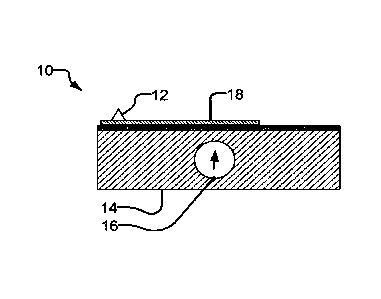
states
that can represent data. An example of a qubit is the quantum spin of a
particle that
can be oriented parallel to ("spin down") or anti-parallel to ("spin up") a
magnetic field.
The spin up state may, for example, be associated with a logical "1" and the
spin
down state may be associated with a logical "0".
[0014] "Quantum measurement" means a process by which a value is determined
for
a measurable quantity of a quantum system. An example of quantum measurement
is
a process that determines whether a spin of a quantum particle is spin up or
spin
2
Date Recue/Date Received 2023-01-23
CA 03189846 2023-01-23
down. Where a quantum system is in a superposition of quantum states and the
measurable quantity has a different value for each of the quantum states then
a result
of quantum measurement is that the quantum system will be in the one of the
quantum states corresponding to the determined value immediately after the
quantum
measurement.
[0015] "Superposition" when applied to a quantum particle or other quantum
system
means that the quantum system exists in two or more separate quantum states at
the
same time. For example, a quantum particle that has non-zero spin in a
magnetic
field may simultaneously be in two different spin states.
Summary
[0016] The present technology has various aspects. These include, without
limitation:
= systems and methods for extending coherence times of qubits in quantum
computers;
= systems and methods for providing data to and reading data from qubits in
quantum computers;
= systems and methods for using optical photons to interact with qubits in
which
states are separated by sub-optical energies;
= systems and methods for quantum computing;
= systems and methods for entangling microwave and optical photons;
These aspects may be applied individually or in any combinations.
[0017] One aspect of the invention provides a method for storing quantum
information. The method comprises providing a first qubit in a first quantum
state that
encodes first quantum information. The first qubit has first and second
quantized
energy levels separated by an energy AEscl corresponding to a microwave
frequency.
In some embodiments the first qubit comprises a superconducting qubit. The
method
comprises coupling the first qubit to a first luminescent center in silicon by
way of a
microwave photon state such that quantum states of the first qubit and the
first
luminescent center undergo a quantum interaction wherein the quantum state of
the
first luminescent center encodes the first quantum information.
[0018] Some embodiments comprise uncoupling the first qubit from the first
luminescent center.
[0019] Some embodiments comprise coupling the first qubit to the first
luminescent
center for a time that is substantially equal to n half periods of a two qubit
Rabi
3
Date Recue/Date Received 2023-01-23
CA 031.89846 2023-01-23
frequency of the first qubit and the first luminescent center wherein n is an
odd
integer.
[0020] In some embodiments the first luminescent center has first and second
quantized energy levels separated by an energy AELC1 and coupling the first
qubit to
the first luminescent center comprises adjusting one or both of the energy
AELci and
the energy ilEsci so that LiELci and LlEsci are substantially equal.
[0021] Some embodiments comprise adjusting the energy AEL.ci by applying an
electric field to the first luminescent center. Some embodiments comprise
adjusting
the energy AELci by applying an RF driving signal to the first luminescent
center.
Some embodiments comprise adjusting the energy AELci by applying a strain to
the
silicon in which the first luminescent center is located. In some embodiments
the first
luminescent center is in a magnetic field and the method comprises adjusting
the
energy AELci by varying a strength of the magnetic field at the luminescent
center.
[0022] In some embodiments the first luminescent center possesses a third
energy
level separated from the first energy level by an energy difference AEL.c2 and
the
method comprises coupling the quantum state of the first luminescent center to
a
photon state in a first resonator having a resonant frequency corresponding to
LiELc2
such that the photon state in the first resonator encodes the first quantum
state. In
some embodiments the photon state in the first resonator is an optical photon
state.
In some embodiments the photon state in the first resonator corresponds to an
optical
wavelength in the range of about 1pm to about 5pm.
[0023] Some embodiments comprise delivering a photon of the photon state to a
second resonator and coupling the second resonator to a second luminescent
center
such that a quantum state of the second luminescent center encodes the first
quantum information.
[0024] In some embodiments the photon state in the first resonator is
entangled with
another photon state in a second resonator and the method comprises coupling
the
second resonator to a second luminescent center such that a quantum state of
the
second luminescent center encodes the first quantum information.
[0025] Some embodiments comprise encoding the first quantum information in a
quantum state of a second matter qubit by coupling the second luminescent
center to
the second matter qubit by way of another microwave photon state wherein
quantum
states of the second matter qubit and the second luminescent center engage in
a
quantum interaction such that the quantum state of the second matter qubit
encodes
4
Date Recue/Date Received 2023-01-23
CA 03189846 2023-01-23
the first quantum information. Some embodiments comprise uncoupling the second
matter qubit from the second luminescent center. Some embodiments comprise
entangling the photon state with three or more luminescent centers. Some
embodiments comprise returning the first quantum information to the first
qubit by
coupling the first luminescent center to the first qubit by way of another
microwave
photon state such that quantum states of the first qubit and the first
luminescent
center engage in a quantum state transfer interaction such that the quantum
state of
the first qubit encodes the first quantum information.
[0026] In some embodiments the first luminescent center comprises a crystal
defect
in a silicon crystal. In some embodiments the first luminescent center
comprises an
ensemble of luminescent centers wherein each of the luminescent centers in the
ensemble comprises a crystal defect in a silicon crystal.
[0027] In some embodiments the crystal defect comprises a T center. In some
embodiments the crystal defect has an unpaired ground state spin and comprises
an I
center or an M center or an All center or a Gal center or a Nitrogen-Carbon
center or
a silicon damage center.
[0028] In some embodiments wherein the crystal defect comprises at least one
of an
electron having an electron spin and a hole having a hole spin and the first
and
second quantized energy levels of the first luminescent center respectively
comprise
spin down and spin up states of the electron or hole. In some embodiments the
crystal defect comprises at least one nuclear spin and the method further
comprises
encoding a quantum state of the electron or hole in a quantum state of the
nuclear
spin such that the nuclear spin encodes the first quantum information.
[0029] In some embodiments the crystal defect comprises at least one unpaired
electron or hole spin and at least one nuclear spin and the method further
comprises
encoding the first quantum information in a joint quantum state of the at
least one
unpaired electron or hole spin and the at least one nuclear spin. In some
embodiments encoding the first quantum information in the joint quantum state
of the
unpaired electron or hole spin and the nuclear spin comprises causing a cross
transition. In some embodiments the cross transition comprises an electron
dipole
spin resonance (EDSR) transition. Some embodiments comprise recovering the
first
quantum information by setting the unpaired electron or hole spin to have an
initialized quantum state and causing a spin transition of the unpaired
electron or hole
spin and/or the nuclear spin.
Date Recue/Date Received 2023-01-23
CA 03189846 2023-01-23
[0030] In some embodiments the crystal defect comprises a plurality of nuclear
spins
and the method comprises:
encoding the first quantum information in a first one of the nuclear spins;
causing the first qubit to encode second quantum information;
coupling the first qubit to the first luminescent center by way of a second
microwave
photon state such that quantum states of the first qubit and an electron or
hole of the
first luminescent center undergo a quantum interaction and the quantum state
of the
electron or hole of the first luminescent center encodes the second quantum
information;
uncoupling the first qubit from the first luminescent center; and
encoding the quantum state of the electron or hole in a quantum state of a
second
one of the nuclear spins such that the second one of the nuclear spins encodes
the
second quantum information.
[0031] Some embodiments comprise creating a bound exciton by illuminating the
crystal defect center with an optical pulse prior to coupling the first qubit
to the first
luminescent center. Some embodiments comprise encoding the first quantum
information in a spin state of the hole. In some embodiments the luminescent
center
comprises an impurity atom in a silicon crystal.
[0032] In some embodiments the impurity atom comprises a double donor atom. In
some embodiments the double donor is a selenium, tellurium or sulphur atom.
[0033] In some embodiments at least 95% of silicon atoms in the silicon
crystal are
silicon-28.
[0034] In some embodiments the first qubit is in a first refrigerator and the
second
matter qubit is in a second refrigerator and the first and second resonators
are
connected by an optical path that passes outside of the first and second
refrigerators.
In some embodiments at least a portion of the optical path that is outside of
the first
and second refrigerators is at a temperature that is greater than AEsct kB
where kB is
Boltzmann's constant In some embodiments the optical path comprises an optical
fiber. In some embodiments AEBQ is 1.3 meV or less.
[0035] In some embodiments the first qubit is a superconducting qubit In some
embodiments the first qubit comprises a quantum dot or an ion trap.
[0036] Another aspect of the invention provides a method for transferring a
quantum
state of a superconducting qubit to an optical photon. The method comprises
coupling
a superconducting qubit having two quantum states having corresponding energy
6
Date Recue/Date Received 2023-01-23
CA 031.89846 2023-01-23
levels separated by an energy AEI to a luminescent center in silicon having
first and
second quantum states having corresponding energy levels separated by an
energy
near AEi and third and fourth quantum states having corresponding energy
levels that
are respectively separated from the energy levels corresponding to the first
and
second states by energies AE2 and AE3 and subsequently coupling the
luminescent
center to an optical structure that supports a photon mode having a frequency
corresponding to the energy AE2 and/or AE3.
[0037] In some embodiments AE2 #AE3 .
[0038] In some embodiments coupling the superconducting qubit to the
luminescent
center is performed by way of a resonator having a microwave resonant
frequency
corresponding to the energy AEi .
[0039] Some embodiments comprise maintaining the coupling between the
superconducting qubit and the luminescent center for a time equal to an odd
number
of periods of a two qubit Rabi frequency for the coupled superconducting qubit
and
the luminescent center and then uncoupling the superconducting qubit and the
luminescent center.
[0040] In some embodiments the optical structure is an optical resonator.
[0041] Some embodiments comprise detecting a photon in the optical structure.
[0042] Another aspect of the invention provides a method for transferring a
quantum
state of a superconducting qubit to an optical photon. The method comprises
entangling the quantum state of the superconducting qubit with a quantum state
of a
luminescent center by way of a microwave photon; and subsequently entangling
the
quantum state of the luminescent center with an optical photon state.
[0043] Some embodiments comprise manipulating the quantum state of the
luminescent center prior to entangling the quantum state of the luminescent
center
with the optical photon state.
[0044] Another aspect of the invention provides a method for storing first
quantum
information. The method comprises coupling a qubit having a first quantum
state with
an electron spin or a hole spin in a T center in silicon to transfer the first
quantum
state to a quantum state of the electron spin or hole spin; and, uncoupling
the
electron spin or hole spin from the qubit.
[0045] Some embodiments comprise subsequently causing a quantum interaction
between the quantum state of the electron spin or hole spin with a quantum
state of a
first nuclear spin of a plurality of nuclear spins of the T center such that
some or all of
7
Date Recue/Date Received 2023-01-23
CA 03189846 2023-01-23
the first quantum information is encoded in the first nuclear spin.
[0046] Some embodiments comprise setting the qubit to have a second quantum
state; and
coupling the qubit with the electron spin or hole spin in the T center to
transfer the
second quantum state to the electron spin or hole spin.
[0047] Some embodiments comprise uncoupling the electron spin or hole spin
from
the qubit; and
subsequently transferring the quantum state of the electron spin or hole spin
to a
quantum state of a second nuclear spin of the plurality of nuclear spins of
the T
center.
[0048] Another aspect of the invention provides an apparatus for storing
quantum
information. The apparatus comprises: a first qubit having first and second
quantized
energy levels separated by an energy AESQ corresponding to a microwave
frequency;
a luminescent center in silicon having first and second quantized energy
levels
separated by an energy ZIELci; and means for coupling the first qubit to the
luminescent center by way of a microwave photon.
[0049] In some embodiments the first qubit is a superconducting qubit.
[0050] In some embodiments the first qubit is a quantum dot or an ion trap.
[0051] In some embodiments the means for coupling comprises a microwave
resonator.
[0052] In some embodiments the means for coupling comprises a means for
adjusting one or both of the energy AELci and the energy AEsQ so that AELc,
and
LEso are substantially equal.
[0053] Some embodiments comprise means for coupling the first qubit to the
luminescent center for a time that is substantially equal to n half periods of
a two qubit
Rabi frequency of the first qubit and the luminescent center wherein n is an
odd
integer.
[0054] In some embodiments the luminescent center comprises a T center.
[0055] In some embodiments the luminescent center comprises an ensemble of T
centers.
[0056] Some embodiments comprise means for selectively coupling an unpaired
electron of the T center to a nuclear spin of the T center.
[0057] In some embodiments the luminescent center is in a silicon substrate
and the
first qubit is supported on the silicon substrate.
8
Date Recue/Date Received 2023-01-23
CA 03189846 2023-01-23
[0058] Another aspect of the invention provides an apparatus for transferring
a
quantum state of a superconducting qubit to an optical photon. The apparatus
comprises: a superconducting qubit having two quantum states having
corresponding
energy levels separated by an energy AE1; a luminescent center in silicon
having first
and second quantum states having corresponding energy levels separated by an
energy near AEi and third and fourth quantum states having corresponding
energy
levels that are respectively separated from the energy levels corresponding to
the first
and second quantum states by energies AE2 and AE3; means for coupling the
superconducting qubit to the luminescent center; and, means for coupling the
luminescent center to an optical structure that supports a photon mode having
a
frequency corresponding to the energy AE2 and/or AE3.
[0059] Another aspect of the invention provides a method for creating quantum
entanglement among a plurality of spaced-apart qubits. Each of the qubits have
first
and second quantized energy levels separated by an energy AEso corresponding
to a
microwave frequency. The method comprises coupling each of the qubits to a
corresponding luminescent center in silicon by way of microwave photon states,
the
luminescent center having at least first, second and third quantized energy
levels
wherein the first and second energy levels are separated by an energy
difference
corresponding to an energy of the microwave photon states and the first and
third
energy levels are separated by an energy difference corresponding to an energy
of
optical photons; and, coupling each of the luminescent centers to the other
ones of
the corresponding luminescent centers by way of an optical structure that
supports
one or more optical photon states having energies corresponding to a quantum
transition of the luminescent center between the first and third energy
levels.
[0060] Another aspect of the invention provides a method for quantum
computing.
The method comprises: storing quantum information as a qubit state in a defect
in a
silicon crystal wherein the defect comprises a plurality of impurity atoms
that
collectively include at least one unpaired electron having a corresponding
electron
spin state and a plurality of nuclear spins each having a corresponding
nuclear spin
state; and setting one of the spin states to represent the qubit information
and using a
plurality of the nuclear spins for quantum error correction or error detection
for the
qubit information.
[0061] Some embodiments comprise using the plurality of nuclear spins for
majority
voting local error correction.
9
Date Recue/Date Received 2023-01-23
CA 03189846 2023-01-23
[0062] Some embodiments comprise using the plurality of nuclear spins as
ancillas
for encoding the qubit information in a logical qubit.
[0063] In some embodiments the defect comprises a T center, an I center or an
M
center.
[0064] In some embodiments the defect comprises a T center.
[0065] In some embodiments energy levels of transitions between different
nuclear
spin states of the nuclear spins are different for different ones of the
nuclear spins.
[0066] Another aspect of the invention provides a method for quantum
entanglement
purification. The method comprises: providing first and second defects in a
silicon
crystal wherein the first and second defects each comprise an operational
qubit
comprising an electron or hole spin and at least one memory qubit comprising a
nuclear spin; and entangling quantum states of the operational qubits of the
first and
second defects; transferring the entanglement to the at least one memory qubit
of
each of the first and second defects by state transfer.
[0067] Some embodiments comprise repeating the steps of: entangling quantum
states of the operational qubits of the first and second defects; and
transferring the
entanglement to the at least one memory qubit of each of the first and second
defects
by state transfer.
[0068] In some embodiments the defect comprises a T center, an I center or an
M
center. In some embodiments the defect comprises a T center.
[0069] Another aspect of the invention provides a method for storing quantum
information in a defect in a silicon crystal. The method comprises: setting a
quantum
state of an electron or hole spin of the defect to encode first quantum
information and
initializing a first nuclear spin of the defect to a first initial nuclear
spin state; and
illuminating the defect with first photons that have a first wavelength
matching the
energy of a first spin transition that involves the electron or hole spin and
the first
nuclear spin.
[0070] Some embodiments comprise setting a quantum state of the electron or
hole
spin of the defect to encode second quantum information and initializing a
second
nuclear spin of the defect to a second initial nuclear spin state; and
illuminating the
defect with second photons that have a second wavelength matching the energy
of a
second spin transition that involves the electron or hole spin and the second
nuclear
spin.
[0071] In some embodiments the first transition is a cross transition.
Date Recue/Date Received 2023-01-23
CA 03189846 2023-01-23
[0072] In some embodiments the first photons are provided in the form of a
coherent
pi pulse.
[0073] In some embodiments the defect comprises a T center, an I center or an
M
center.
[0074] In some embodiments the defect comprises a T center.
[0075] Further aspects and example embodiments are illustrated in the
accompanying drawings and/or described in the following description.
[0076] It is emphasized that the invention relates to all combinations of the
above
features, even if these are recited in different claims.
Brief Description of the Drawings
[0077] The accompanying drawings illustrate non-limiting example embodiments
of
the invention.
[0078] Fig 'I illustrates schematically a system that includes a short lived
qubit and
apparatus for extending a lifetime of the short lived qubit.
[0079] Fig. 'IA schematically illustrates energies of quantum states of a
short lived
qubit and a long lived qubit and the interactions of photons with the short
lived and
long lived qubits.
[0080] Fig. 2 is a graph illustrating the evolution of probability densities
for two
coupled quantum systems.
[0081] Fig. 3 is a flow chart illustrating an example method for preserving a
quantum
state of a short lived qubit
[0082] Fig. 4 is a schematic illustration showing a construction for an
example system
that includes a short lived qubit and a long lived qubit.
[0083] Fig. 5 is a schematic illustration showing a qubit that couples to both
microwave and optical photons arranged to couple quantum information to an
external system.
[0084] Fig 6 is an example energy level diagram for quantum states in a qubit
that
may couple to both microwave and optical photons.
[0085] Fig. 6A is a schematic view showing long lived qubits located to couple
to
microwave photons by electric field or magnetic field interactions.
[0086] Fig. 6B is a schematic view showing energy levels for a quantum system
that
can include a bound exciton in which a hole spin state can serve as a long
lived qubit
[0087] Figs. 7A and 7B are respectively cross section and plan views that
schematically illustrate a system in which a qubit is arranged for coupling to
optical
11
Date Recue/Date Received 2023-01-23
CA 03189846 2023-01-23
photons.
[0088] Fig. 8 is a schematic view showing a system in which qubits in plural
refrigerators can be coupled by optical photons.
[0089] Fig. 9 shows the structure of a T center in silicon.
Detailed Description
[0090] Throughout the following description, specific details are set forth in
order to
provide a more thorough understanding of the invention. However, the invention
may
be practiced without these particulars. In other instances, well known
elements have
not been shown or described in detail to avoid unnecessarily obscuring the
invention.
Accordingly, the specification and drawings are to be regarded in an
illustrative, rather
than a restrictive sense.
[0091] One aspect of this invention provides apparatuses which extend
lifetimes of
qubits. The qubits may, for example comprise superconducting qubits. One
disadvantage of superconducting qubits is that their lifetime is undesirably
short
(usually with coherence times on the order of 100 ps or shorter). This
interferes with
the ability to process quantum information using superconducting qubits.
[0092] Fig. 1 illustrates schematically a system 10 that includes a short
lived qubit 12.
Short lived qubit 12 may, for example comprise a superconducting qubit such as
a
transmon or other charge-based or flux-based superconducting qubit.
[0093] System 10 takes advantage of the fact that qubits provided in a silicon
crystal
can have lifetimes several orders of magnitude longer than short lived qubits
such as
superconducting qubits. System 10 includes a body 14 made of silicon.
Preferably but
optionally body 14 comprises the purified isotope of silicon that has an
atomic weight
of 28 ("silicon 28"). Body 14 may, for example, be a part of a substrate on
which short
lived qubit 12 is formed. Body 14 includes at least one long lived qubit 16.
[0094] Long lived qubit 16 may, for example comprise an unpaired spin (e.g. an
electron spin or a nuclear spin or a hole spin in an exciton) or a number of
excitons.
An exciton may, for example, be created by illuminating a luminescent center
with
optical radiation having a frequency corresponding to an energy of the
exciton.
[0095] Long lived qubit 16 may be provided by one or more particles or quasi
particles in a luminescent center. In some embodiments a luminescent center is
provided by a crystal defect in body 14 such as a color center that has an
unpaired
ground state spin (e.g. a T center, an I center, or an M center, an All center
or a Gal
center, or a Nitrogen-Carbon centre, or a spin-active silicon radiation damage
center
12
Date Recue/Date Received 2023-01-23
CA 03189846 2023-01-23
or a silicon color center with an unpaired ground state spin). Where the
luminescent
center is a crystal defect the particles or quasi particles may, for example,
be
electrons, holes, atomic nuclei, or excitons of the luminescent center. Some
types of
crystal defects provide plural particles or quasi particles that may be used
individually
or in groups to provide long lived qubits. For example, a T centre has at
least three
nuclear spins, an electron spin, a possibility of a hole spin in a bound
exciton and an
exciton number which may all be used as long lived qubits 16.
[0096] In some cases a crystal defect may include one or more impurity atoms.
In
some embodiments a luminescent center is provided by an impurity atom in which
case long lived qubit 16 may be provided by one or both of an electron spin
and a
nuclear spin of the impurity atom.
[0097] In some embodiments long lived qubit 16 comprises an unpaired spin
provided
by an atom of an impurity such as selenium or sulphur or tellurium in a
silicon crystal.
[0098] System 10 also includes a controllable coupling 18. Coupling between
short
lived qubit 12 and long lived qubit 16 by way of coupling 18 can be controlled
to
selectively allow short lived qubit 12 and long lived qubit 16 to interact
with one
another.
[0099] Coupling 18 is configured to permit sufficiently strong coupling
between short
lived qubit 12 and long lived qubit 16 to facilitate state-transfer between or
entanglement of short lived qubit 12 and long lived qubit 16. The coupling
may, for
example, comprise a resonator designed to accommodate photons having energies
corresponding to quantum transitions of short lived qubit 12 and long lived
qubit 16.
[0100] One measure of the strength of coupling between short lived qubit 12
and long
lived qubit 16 is the two-qubit Rabi frequency which is described elsewhere
herein.
The two qubit Rabi frequency increases as the coupling between the two qubits
becomes stronger. To facilitate efficient quantum interaction between short
lived qubit
12 and long lived qubit 16 the period of the Rabi frequency should be larger
than the
coherence times of short lived qubit 12 and long lived qubit 16. For example,
one can
define "cooperativity" as follows:
2
C = __________________________________ j
RSL * RLL
where C is the cooperativity, fR is the Rabi frequency, RSL is the decoherence
rate
(i.e. the inverse of the decoherence time) for the short lived qubit and RLL
is the
decoherence rate for the long lived qubit. In some embodiments the strength of
the
13
Date Recue/Date Received 2023-01-23
CA 03189846 2023-01-23
coupling is given by a cooperation value C.1 when coupling 18 is coupling
short lived
qubit 12 to long lived qubit 16.
[0101] In some embodiments C>1 is achieved with a two-qubit Rabi frequency of
less
than 50 kHz. For example, where short lived qubit 12 has a coherence time of 1
ps
(which is typical for some superconducting qubits) and long lived qubit 16 has
a
coherence time of 1 ms (which is typical for an electron spin in a T center)
then C>1
can be achieved with a two qubit Rabi frequency of 30 kHz or more. As another
example, where short lived qubit 12 has a coherence time of 1 ps and long
lived qubit
has a coherence time on the order of Is (which is typical for a nuclear spin
in a T
center in silicon) a two qubit Rabi frequency of 1 kHz or more is sufficient
to achieve
c>1-
[0102] The Rabi frequency may be increased by increasing the strength of
coupling
between short lived qubit 12 and long lived qubit 16. This may be achieved,
for
example by one or more of:
= making transition energies of short lived qubit 12 and long lived qubit
16 match
more closely;
= making short lived qubit 12 and long lived qubit 16 physically closer to
one
another;
= more closely matching a resonant frequency of a coupling 18 (e.g. a
resonator) to the transition energies of short lived qubit 12 and long lived
qubit
16;
= providing a geometry in which short lived qubit 12 and long lived qubit
16 can
each couple to antinodes of electromagnetic modes that couple short lived
qubit 12 and long lived qubit 16.
[0103] Short lived qubit 12 may represent qubit values in various ways, for
example,
constructions of superconducting qubits in which quantum information is stored
by
phase, charge or flux are all known.
[0104] In some embodiments, coupling 18 comprises a resonator arranged so that
a
maximum of an electromagnetic field associated with a short lived qubit 12
couples to
the resonator. For example, where short lived qubit 12 is a superconducting
flux qubit,
the resonator may be inductively coupled to a magnetic field antinode of the
superconducting flux qubit. As another example, where short lived qubit 12 is
a
superconducting charge qubit or a superconducting phase qubit the resonator
may be
capacitively coupled at an electric field antinode of short lived qubit 12.
14
Date Recue/Date Received 2023-01-23
CA 03189846 2023-01-23
[0105] A resonator of coupling 18 may be arranged so that an electromagnetic
field
maximum of a photonic mode supported by the resonator is located at or close
to the
location of long lived qubit 16.
[0106] In some embodiments coupling 18 is provided by a direct interaction of
an
electromagnetic field of short lived qubit 12 with long lived qubit 16. In
such
embodiments, coupling 18 is provided by the relative physical arrangement of
short
lived qubit 12 relative to long lived qubit 16 which allows them to be coupled
for
quantum interaction as described herein. Long lived qubit 16 may be located at
or
near to a point at which the electromagnetic field associated with short lived
qubit 12
has a maximum. For example, where short lived qubit 12 comprises a
superconducting flux qubit comprising a flux loop, a long lived qubit 16 (e.g.
a T
centre) may be located inside the flux loop where it can couple directly to a
magnetic
field produced by the flux loop. Where short lived qubit 12 is a charge or
phase qubit,
long lived qubit 16 may be located at or close to an electric field maximum of
the
electric field produced by the short lived qubit 12. In some embodiments, long
lived
qubit 16 is at a location where the electromagnetic field of short life qubit
12 with
which long life qubit 16 interacts has a strength that is no more than 3 dB
lower or 2
dB lower than a strength of the electromagnetic field at a location where the
electromagnetic field has maximum strength.
[0107] In some embodiments the energy difference between quantum states of
each
of short lived qubit 12 and long lived qubit 16 correspond to photon
frequencies in the
radiofrequency (RF) or microwave region. For example, in some embodiments
photon
frequencies are in the range of about 1 MHz to 100 GHz. In some embodiments
the
photon frequencies are in the range of 1 GHz to 100GHz. In some embodiments
the
photon frequencies are in the range of 3 GHz to 8 GHz.
[0108] The relationship between energy and photon frequency is given by the
relationship:
E =1w
Where E is the energy difference, h is Planck's constant and v is the photon
frequency. Photon frequency is related to photon wavelength by:
U¨ ch
Where c is the speed of light and A is the photon wavelength.
[0109] System 10 may comprise a mechanism operative to cause the energy
difference AEs between quantum states in short lived qubit 12 and the energy
Date Recue/Date Received 2023-01-23
CA 03189846 2023-01-23
difference AEL between quantum states in long lived qubit 16 to be equal or
close to
equal. Those of skill in the art will understand that short lived qubit 12 and
long lived
qubit 16 can engage in quantum interactions (e.g. state transfer or quantum
entangling operations) even if there are small differences between AEs and AEL
. For
convenience, in this disclosure when two energies are stated to be "equal"
(e.g. as in
AEs=AEL) what is meant is that the two energies are exactly equal or close
enough to
being equal for the described purpose (e.g. entanglement of two quantum
systems).
Similarly, when two frequencies are said to be equal or to match (e.g. a
resonant
frequency of a resonator and a frequency of a photon) what is meant that the
two
frequencies are exactly equal or close enough to being equal for the desired
purpose
(e.g. excitation of a photon mode in the resonator).
[0110] How closely AEs and AEL need to be made to be equal to one another to
achieve desired quantum interactions will depend on factors such as the
strength of
coupling between short lived qubit 12 and long lived qubit 16 and linewidths
of the
quantized transitions of short lived qubit 12 and long lived qubit 16. In some
embodiments the energy difference AEs between quantum states in short lived
qubit
12 and the energy difference AEL between quantum states in long lived qubit 16
are
made to be equal within 1% or 1/2% or 1 part in 10000.
[01111 In some embodiments AEs and AEL are non-equal unless one or both are
controlled to achieve AEs=AEL. Such a mechanism may adjust one or both of AEs
and AEL for example by applying magnetic, electric, or RF control fields to
short lived
qubit 12 and/or long lived qubit 16 and/or by applying strain to a substrate
in which
long lived qubit 16 is located.
[0112] System 10 optionally also includes a mechanism for adjusting the
coupling
between short lived qubit 12 and long lived qubit 16. This mechanism may, for
example comprise an adjustable resonator that has a resonant frequency that is
adjustable to either match or not match the frequency of photons having
energies
equal to AEs and AEI._
[0113] When AEs# AEL and/or the coupling between short lived qubit 12 and long
lived qubit 16 is disabled in some other manner then quantum states of short
lived
qubit 12 and long lived qubit 16 can evolve essentially independently of one
another.
[0114] When AEs= AEL and the coupling between short lived qubit 12 and long
lived
qubit 16 is sufficient the quantum states of short lived qubit 12 and long
lived qubit 16
may become entangled by way of microwave photons. This is illustrated in Fig.
1A.
16
Date Recue/Date Received 2023-01-23
CA 03189846 2023-01-23
[0115] Fig. IA shows schematically states 12H and 12L of short lived qubit 12
and
states 16H and 16L of long lived qubit 16. Short lived qubit 12 can emit a
photon 19
and transition from state 12H to 12L. Short lived qubit 12 can absorb a photon
19 and
transition from state 12L to 12H. Long lived qubit 16 can emit a photon 19 and
transition from state 16H to 16L. Long lived qubit 16 can absorb a photon 19
and
transition from state 16L to 16H.
[0116] Because qubits 12 and 16 are quantum systems, in the absence of a
quantum
measurement, a larger system including qubit 12, qubit 16 and photons 19 can
exist
in a superposition of states which may include states in which either or both
of qubits
12 and 16 has emitted a photon 19 and states in which either or both of qubits
12 and
16 has absorbed a photon 19. The states of qubits 12 and 16 are entangled with
one
another and with the states of photons 19 by which their quantum states are
coupled.
[0117] Coherent coupling of short lived qubit 12 and long lived qubit 16 may
be
selectively enabled, for example to entangle quantum states of short lived
qubit 12
and long lived qubit 16 and/or to transfer a quantum state of short lived
qubit 12 to
long lived qubit 16 and/or to transfer a quantum state of long lived qubit 16
to short
lived qubit 12, by adjusting one or more of:
=
= AEL and
= the coupling between qubits 12 and 16.
[0118] In some embodiments, coupling between short lived qubit 12 and long
lived
qubit 16 is facilitated by a resonator 20 that has a resonant frequency
corresponding
to the frequency of microwave photons 19 that are emitted/absorbed when short
lived
qubit 12 and long lived qubit 16 transition between quantum states. Resonator
20
may, for example comprise a patch of superconducting material in a circuit
designed
to have a resonant frequency corresponding to photons 19. Resonator 20 may,
for
example, comprise a coplanar waveguide resonator or an LC resonator.
[0119] Resonator 20 may be positioned close enough to each of qubits 12 and 16
to
provide a sufficient level of coupling between each of qubits 12, 16 and
photons 19 in
resonator 20. Capacitive or inductive coupling between a superconducting qubit
12
and resonator 20 can have a relatively long range such that a spacing between
such
a qubit 12 and a resonator 20 can be e.g. a few pm. As another example,
coupling
between a quantum dot used as qubit 12 and resonator 20 typically has a much
shorter range such that resonator 20 is best located closer than about 1 pm or
closer
17
Date Recue/Date Received 2023-01-23
CA 03189846 2023-01-23
than 100 nm to the quantum dot. Coupling between resonator 20 and a long lived
qubit 16 may have a range of a few microns in which case resonator 20 may be
located within a few pm of the long lived qubit 16.
[0120] A mechanism may be provided for adjusting the energy gap between
quantum
states of a qubit. The nature and construction of the mechanism will depend on
the
nature of the quantum system on which the qubit is based. For example:
= Where the qubit is provided by an electron spin or a hole spin or a
nuclear spin
in a magnetic field the energy difference between spin up and spin down
states may be adjusted by changing a strength of the magnetic field at the
location of the electron or nucleus.
= Where the qubit is a superconducting qubit the energy difference between
states may be adjusted by adjusting the quantized magnetic flux through a
superconducting circuit that implements the superconducting qubit This may
be done, for example, by altering a capacitance or inductance of the
superconducting circuit.
= Where the qubit is provided by an atom or defect in a crystal lattice
then
energy levels of the qubit may be altered by applying strain to the crystal
lattice.
= Where the qubit is provided by an electron spin or a hole spin or a
nuclear spin
in a magnetic field the energy levels of the qubit may be adjusted by applying
an RF driving field to the qubit. The frequency of the RF driving field may,
for
example be set to be in a range such that the energy of photons of the RF
driving field is at least approximately equal (e.g. within about 1% or 4% or
one
part in 10000) to the energy difference between the energy levels of the
qubit.
The energy levels of the qubit may be varied by adjusting the frequency of the
RF driving field and/or the amplitude of the RF driving field.
= Where the qubit is provided by an electron spin or a hole spin or a
nuclear spin
in a magnetic field the energy levels of the qubit may be adjusted by applying
an electric field at the location of the qubit. In some embodiments the
electric
field is oriented to be parallel to an orientation of the magnetic field.
[0121] When short lived qubit 12 and long lived qubit 16 are coupled by
coupler 18 as
described above, energy can be transferred back and forth between short lived
qubit
12 and long lived qubit 16 by way of photons 19. The possibility for such
energy
transfer results in an oscillation of a probability density function which
indicates the
18
Date Recue/Date Received 2023-01-23
CA 03189846 2023-01-23
probability of finding short lived qubit 12 in a particular quantum state
(e.g. 12H or
12L). This oscillation occurs at the so-called two-qubit Rabi frequency which
depends
on the coupling between short lived qubit 12 and long lived qubit 16.
[0122] The Rabi frequency can be determined in advance. The two-qubit Rabi
frequency may be measured in a calibration step. The calibration step may, for
example, comprise initializing long lived qubit 16 and short lived qubit 12
into known
quantum states, turning on the coupling for some time 'tau', turning off the
coupling,
and then independently measuring both of qubits 12 and 16. By repeating this
measurement sequence for different values of tau one can obtain a plot like
that
shown in Fig. 2 from which the Rabi frequency can be readily determined. The
Rabi
frequency determined by the calibration step may be stored in a data store for
future
use. For example, the data store may comprise a memory location accessible to
a
control circuit connected to control the coupling between long lived qubit 16
and short
lived qubit 12 using any of the mechanisms described herein.
[0123] Fig. 2 is a graph showing the probability density for short lived qubit
12 being
in the higher-energy level of two non-degenerate binary quantum states (curve
22A)
and the probability for long lived qubit 16 being in the higher-energy level
one of two
non-degenerate binary quantum states (curve 22B).
[0124] In Fig. 2, at time 0 short lived qubit 12 is in its higher-energy
quantum state
and long lived qubit 16 is in its lower-energy quantum state. This may be
caused by
making a quantum measurement at time 0 or by manipulating the states of qubits
12,
16. At time 0, system 10 is configured to couple the states of short lived
qubit 12 and
long lived qubit 16.
[0125] The probability density represented by curve 22A cycles with a period
T. At
time T/2 long lived qubit 16 has a high probability of being in its higher
energy state
and short lived qubit 12 has a low probability of being in its lower-energy
quantum
state. In essence, the quantum state of short lived qubit 12 has been
transferred to
long lived qubit 16 and vice versa.
[0126] The principle illustrated in Fig. 2 also applies to other quantum
states of short
lived qubit 12 and long lived qubit 16 and their superpositions.
[0127] As described above, a state of short lived qubit 12 (which may be a
superconducting qubit) can be transferred to a long lived qubit 16 (which may
be a
spin qubit for example), stored in long lived qubit 16 for a period of time
that is longer
than the lifetime of short lived qubit 12, and then returned to short lived
qubit 12 for
19
Date Recue/Date Received 2023-01-23
CA 03189846 2023-01-23
further processing.
[0128] Fig. 3 illustrates a method 30 for extending the lifetime of a quantum
state of
short lived qubit 12. In block 32A short lived qubit 12 is placed into a
desired quantum
state. The quantum state may be a superposition of a higher-energy state and a
lower-energy state. Block 32A may, for example, comprise performing a quantum
computation in a quantum computer of which short lived qubit is a part.
[0129] In block 32B, short lived qubit is coupled to long lived qubit 16, for
example by
a coupler 18 as described above. Block 32B may, for example, comprise
adjusting an
energy difference AEL between the higher-energy and lower energy quantum
states
of long lived qubit 16 and/or adjusting an energy difference MS between the
higher-
energy and lower energy quantum states of short lived qubit 12 to achieve
AEs=AEL.
[0130] In block 32C, the coupling between short lived qubit 12 and long lived
qubit 16
is maintained for a time t equal to an odd number, N (N=1, 3, 5, ...) of half
periods T/2
of the Rabi period (e.g. one half period) and then discontinued (e.g. coupling
may be
discontinued by adjusting one or both of AEs and AEL. so that AEs#AEL and/or
by
changing a resonant frequency of a resonator 20). Time t is significantly
shorter than
the decoherence time of short lived qubit 12.
[0131] The time T for maintaining the coupling between short lived qubit 12
and long
lived qubit 6 may be controlled by a timer that uses a stored value equal to
or derived
from the two-qubit Rabi frequency for the particular pair of short lived qubit
12 and
long lived qubit 16 determined in a calibration step to set the time for which
the
coupling is maintained.
[0132] At the end of block 32C the desired quantum state of short lived qubit
12 has
been transferred to long lived qubit 16.
[0133] In block 32D a time period passes. The time period may have a length
that is
longer than a decoherence time of short lived qubit 12. The time period has a
length
that is shorter than a decoherence time of long lived qubit 16. In some
embodiments
the time period has a length of more than 10 ps or more than 100 ps or more
than Is
or more than 1 minute.
[0134] In block 32E short lived qubit 12 is once again coupled to long lived
qubit 16,
for example by a coupler 18 as described above. Block 32E may operate in the
same
manner described herein for block 32B, for example.
[0135] In block 32F the coupling between short lived qubit 12 and long lived
qubit 16
is maintained for an odd number (N=1, 3, 5, ...) of half periods T/2 of the
Rabi period
Date Recue/Date Received 2023-01-23
CA 03189846 2023-01-23
and then discontinued. Block 32F may be performed as described above for block
32C, for example.
[0136] At the end of block 32F short lived qubit 12 has been restored to the
desired
quantum state.
[0137] Fig. 4 shows a possible simplified physical structure for a system 40
that
provides a short lived qubit 12 and a long lived qubit 16 which can be
selectively
coupled and uncoupled to perform method 30 or other similar methods. System 40
includes a silicon substrate 42. Substrate 42 is preferably purified silicon
28 (i.e.
silicon that is more than 92.23% silicon 28). In some embodiment the material
of
substrate 42 is at least 96% or 99% or 99.5% or 99.9% (by number of atoms)
silicon
28.
[0138] Long lived qubit 16 may be provided by a luminescent center 43 in
substrate
42. For example, the luminescent center may comprise a luminescent center
selected
from: a defect such as a T center, an I center, or an M center, or a Nitrogen-
Carbon
center, or an All or a Gal center, or a radiation damage center with an
unpaired
ground state spin; or an impurity such as an atom of selenium or tellurium or
sulphur
or other double donor impurity.
[0139] Short lived qubit 12 may be provided by a superconducting structure 44
that is
supported on substrate 42. Structure 44 may comprise a patterned layer of a
metal
that is superconducting at low temperatures that has been deposited on
substrate 42.
The layer may, for example comprise a superconducting loop that includes a
Josephson junction. An electrically insulating layer 45 may be present between
superconducting structure 44 and the body of substrate 42 in which luminescent
center 43 is located.
[0140] A coupler (that performs the role described above for coupler 18) may
be
provided by a part 44A of superconducting structure 44 that is designed to
provide a
resonance at a frequency corresponding to an energy to which both of energy
differences AEs and AEL can be made to equal. Part 44A may for example,
comprise
a tab of superconducting material that is in a circuit that has a resonant
frequency in
the microwave range. Part 44A may physically overlie luminescent center 43.
[0141] Luminescent center 43 should be spaced closely enough to part 44A to
couple
to electric or magnetic field components of photons in part 44k To couple to
electric
fields, a luminescent center 43 should have a non-negligible capacitance with
part
44A. In some embodiments, luminescent center 43 is spaced apart from part 44A
by
21
Date Recue/Date Received 2023-01-23
CA 03189846 2023-01-23
a distance on the order of about 1 pm or less or a distance on the order of
100 nm or
less. Preferably part 44A is aligned relative to crystallographic axes of
substrate 42 so
that the electric or magnetic field of the photon mode in part 44A couples
well to
luminescent center 43. In some embodiments the magnetic field of the photon
mode
is non-parallel (e.g. orthogonal) to an external magnetic field applied to
luminescent
center 43.
[0142] Fig 4 also shows an adjustable magnet 46 that is operable to change a
magnitude of a magnetic field at the location of luminescent center 43 (and to
therefore change a difference in energies between spin up and spin down states
of a
spin such as an electron spin used to provide long lived qubit 16). A control
circuit
46A is connected to control adjustable magnet 46 (for example to turn on and
off
coupling between long lived qubit 16 and short lived qubit 12). One or more
permanent magnets 46B in the vicinity of luminescent center 43 may augment the
magnetic field from adjustable magnet 46. Magnets 46B may be deposited on or
in or
near substrate 42.
[0143] It is generally beneficial to minimize the component of the magnetic
field
produced by magnets 46 and 46B that is transverse to a plane of
superconducting
structure 44. This is because the critical magnetic field for thin film
superconductors
(i.e. the magnetic field strength above which the superconductor stops being
superconductive) is typically much lower for transverse (perpendicular)
magnetic
fields than for fields in which field lines are parallel to superconducting
structure 44.
[0144] Fig 4 also shows coils 47 that may be driven by an RF signal source 47A
to
manipulate a quantum state of long lived qubit 16 by a resonance effect (e.g.
electron
spin resonance ¨ "ESR") as is known to those of skill in the art. RF signal
source may
be controlled to produce pulses of radiation such as pi pulses or pi/2 pulses
which,
when delivered, manipulate the quantum state of long life qubit 16.
[0145] Fig. 4 also shows an optional light source 48 arranged to illuminate a
location
of long lived qubit 16. Light source 48 may, for example, emit light having a
wavelength that corresponds to an optical transition of long lived qubit 16,
for
example creation of an exciton. For example, long lived qubit 16 may comprise
an
exciton in a crystalline defect such as a T center. Light source 48 may be
operated to
create the exciton by issuing a pulse of light of the appropriate wavelength.
Quantum
information may then be stored in the exciton, for example in a spin state of
the
exciton. Light source 48 may, for example, comprise a laser. The laser may be
22
Date Recue/Date Received 2023-01-23
CA 03189846 2023-01-23
tunable to emit light having wavelengths corresponding to different optical
transitions
of long life qubit 16.
[0146] Substrate 42 is contained within a refrigerator 49 capable of reaching
cryogenic temperatures at which structure 44 is superconducting. In some
embodiments the operating temperature of structure 44 may be very low (e.g. a
few
mK or a few Kelvins).
[0147] In addition to or as an alternative to storing quantum information, a
system as
described herein may be used as a pathway for transferring quantum information
to
or from a quantum information processing system of which short lived qubit 12
is a
part and/or as a mechanism for generating optical photons which represent a
quantum state of short lived qubit 12.
[0148] Fig. 5 schematically illustrates apparatus 50 according to an example
embodiment in which a quantum communication pathway 52 connects long lived
qubit 16 to an external system 54.
[0149] Quantum information pathway 52 may, for example, carry quantum
information
in the form of optical photons. Quantum information pathway 52 may, for
example
comprise a waveguide 53 which can carry photons that carry quantum
information. In
some advantageous embodiments the optical photons have wavelengths in the
range
of about 1.3 to about 1.7 pm or about 1 pm to about 3 pm.
[0150] Quantum information pathway 52 may be coupled to long lived qubit 16 by
way of an optical resonator 55 that is located in proximity to long lived
qubit 16. To
facilitate coupling of long lived qubit 16 to optical photons in optical
resonator 55, long
lived qubit 16 should have available quantum states that have energy levels
that can
be separated by an energy difference that corresponds to an energy of optical
photons. In this case long lived qubit 16 can undergo allowable transitions in
which it
emits or absorbs optical photons.
[0151] In some cases the photons that can be emitted or absorbed in different
allowable transitions of long lived qubit 16 have different polarizations. In
such cases
the polarization of emitted photons may encode a quantum state of the long
lived
qubit 16 from which the photons are emitted. In some cases long lived qubit 16
becomes entangled with photons that have a certain polarization state and as a
result, quantum information that was represented by the spin state of qubit 16
can be
accessed via the polarization state of the entangled photons.
[0152] Fig. 6 shows a simplified example structure of energy levels for long
lived qubit
23
Date Recue/Date Received 2023-01-23
CA 03189846 2023-01-23
16. Levels 16H and 16L may, for example, correspond to spin up and spin down
states of an unpaired spin (e.g. of an electron or a hole), for example levels
16H and
16L may be the result of hyperfine splitting caused by interactions between
nuclear
and electronic spins at the location of long lived qubit 16. The energy
difference
between levels 16H and 16L may correspond to the energy of photons at
microwave
wavelengths.
[0153] Long lived qubit 16 also has states 17H and 17L that may correspond
respectively to spin up and spin down states of an unpaired spin (e.g. of an
electron
or a hole). States 17H and 17L may be related respectively to states 16H and
16L by
an orbital or an excitonic transition. The energy differences between states
17H and
16H or between states 17L and 16L may correspond to the energy of photons at
optical wavelengths.
[0154] As shown in Fig, 6 the energy difference AE1 between states 16H and 17H
is
different from the energy difference AE2 between states 16L and 17L. In some
embodiments the difference between /1,E1 and AE2 corresponds to a frequency
difference of at least about 1 MHz. (i.e. about 6.6x10-28.1). This creates an
opportunity to provide optical photons that probably will or probably will not
interact
with long lived qubit 16 depending on whether the unpaired spin is spin up or
spin
down.
[0155] For example, when optical photons 66 which have a wavelength
corresponding to an energy that is equal to /1E1 are provided, long lived
qubit 16 may
absorb one of the photons 66 and transition from state 16H to state 17H. Long
lived
qubit 16 may subsequently transition from state 17H to 16H and emit a photon
66
having the same energy AE1.
[0156] Since, however, long lived qubit 16 is a quantum system, long lived
qubit 16 is
not necessarily in a definite quantum state. Instead long lived qubit may be
in a
superposition of states. Also, long lived qubit 16 and optical photons 66 may
together
be in a superposition of states in which long lived qubit 16 has or has not
interacted
with a photon. In general, the quantum state of the quantum system made up of
long
lived qubit 16 and optical photons 66 encompasses a wide variety of possible
interactions between long lived qubit 16 and optical photons 66. Consequently
the
quantum states of long lived qubit 16 and optical photons 66 can be entangled.
[0157] It can be seen that energy structures such as those illustrated in Fig.
6 can be
used to couple a long lived qubit 16 to other quantum objects by either of
microwave
24
Date Recue/Date Received 2023-01-23
CA 03189846 2023-01-23
photons and optical photons. This property may be exploited to store quantum
information in long lived qubit 16 from a selected one of plural sources
and/or to
transfer quantum information from long lived qubit 16 to a selected one or
more of
plural destinations. This property may be exploited to transform quantum
information
from a microwave photon to an optical photon by way of long lived qubit 16
and/or to
transform quantum information from an optical photon to a microwave photon by
way
of long lived qubit 16.
[0158] Long lived qubit 16 may be coupled to microwave photons and/or a short
lived
qubit 12 by various mechanisms. These include:
= coupling via an electrical field; and
= coupling via a magnetic field;
Some embodiments have physical constructions which optimize one or more of
these
coupling mechanisms.
In some embodiments the coupling promotes electron dipole spin resonance
("EDSR") interactions.
[0159] Long lived qubit 16 may couple to an electric field component of a
microwave
photon. To optimize electrical coupling the microwave photon may be present as
a
standing wave mode in a resonator wherein the standing wave mode has one or
more antinodes of maximum electric field strength. Long lived qubit 16 may be
located in close proximity to an antinode of maximum electric field strength
(e.g.
within a few pm of the antinode).
[0160] In apparatus 60 according to an example embodiment illustrated in Fig.
6A
microwave photons may be present in a metallic resonator structure 61 on a
silicon
layer 63. An electrically insulating layer 62, for example, a layer of silicon
dioxide,
separates resonator structure 61 from layer 63. Microwave photons in resonator
structure 61 have a standing wave mode in which an electric field strength is
greatest
at an antinode 64. Long lived qubit 16-1 is located in or on silicon substrate
63
proximate to node 64.
[0161] Electric field interactions have a long enough range that in some
embodiments
a long lived qubit couples to the electric field of a photon that is not in a
resonant
cavity (e.g a photon in an optical waveguide that is proximate to the long
lived qubit
16).
[0162] Long lived qubit 16 may couple to a magnetic field component of a
microwave
photon. To optimize electromagnetic coupling the microwave photon may be
present
Date Recue/Date Received 2023-01-23
CA 03189846 2023-01-23
as a standing wave mode in a resonator wherein the standing wave mode has one
or
more antinodes of maximum magnetic field strength and/or one or more antinodes
of
maximum electric field strength. For example, long lived qubit 16 may be
located in
close proximity to (e.g. within a few pm of) an anti node of maximum magnetic
field
strength. For example, Fig. 6A shows a long lived qubit 16-2 located in or on
silicon
substrate 63 in close proximity to an antinode 65 at which magnetic field
strength for
the standing wave mode is maximized.
[016311n some embodiments resonator structure 61 comprises a coplanar
waveguide
("CPW") resonator. A CPW resonator may comprise a coplanar waveguide with a
signal pin segmented into a stub that is capacitively coupled to signal
feedlines. A
CPW resonator can support standing wave resonance at a frequency that depends
on the length of the stub. Electric field antinodes are located at ends of the
stub.
[0164] In some embodiments, resonator structure 61 has a high quality factor
("Q
factor"). The Q factor is the ratio of the center frequency of the resonator
to the
bandwidth of the resonator. In some embodiments resonator structure 61 has a Q
factor of at least 105 or at least 106.
[0165] The notation I a) indicates a quantum state where an electron (or hole)
represented by a first arrow is spin down and a nucleus represented by a
second
arrow is spin up.
[0166] Spin transitions can occur in a system in which a bound exciton may be
created. The quantum number 0 may indicate no bound excitons and the quantum
number 1 may indicate that one bound exciton is present In notation indicating
the
quantum state of a system that can include an exciton state, an electron (or
hole) spin
state and a nuclear spin state the exciton quantum number may be followed by
the
electron (hole) spin followed by the nuclear spin. For example the notation 11
141)
indicates a quantum state in which there is one bound exciton, a hole is spin
down
and a nuclear spin is spin up. This notation is used in the right hand column
of Fig.
6B.
[0167] In the system illustrated in Fig. 6B a bound exciton may be created
when a
photon having energy AEA is absorbed. In a T center AEA corresponds to a
photon
wavelength of about 1326 nm. A bound exciton may be created by directing light
having this wavelength at a T center. When a bound exciton is present the
system of
upper energy levels 67A, 67B, 67C, 67D shown on the right side of Fig 6B is
available. When a bound exciton is not present, only the lower energy levels
66A,
26
Date Recue/Date Received 2023-01-23
CA 03189846 2023-01-23
66B, 66C, 66D are available. It is possible for a T center to be in a
supersposition of
states including a state in which a bound exciton is present and another state
in which
the bound exciton is not present.
[0168] Transitions are possible between any of the energy levels on the right
hand
side of Fig. 6B. These transitions can be categorized as:
= transitions which flip an electron or hole spin but not a nuclear spin
(e.g.
electron paramagnetic resonance (EPR) transitions). Transitions 69C1, 69C2,
6901 and 6902 are examples of transitions in which only an electron or hole
spin flips;
= transitions which flip a nuclear spin but not an electron spin (e.g.
nuclear
magnetic resonance (NMR) transitions). Transitions 69C3, 69C4, 6903 and
6904 are examples of transitions in which only a nuclear spin flips;
= cross transitions in which both an electron or hole spin and a nuclear
spin flip.
(e.g. EDSR transitions). Transitions 69C5, 69C6, 6905 and 6906 are
examples of cross transitions.
= transitions are also possible between states which include a bound
exciton
and states which do not include a bound exciton (e.g. transitions from one of
states 66A, 66B, 66C, 66D to one of states 67A, 67B, 67C, 670).
[0169] In a quantum system such as a T center which includes plural nuclear
spins,
the energy levels of the transitions will, in general, be different for
different ones of the
nuclear spins. A particular available nuclear spin may be selected for a
quantum
interaction with another qubit by a selected one of the above transitions by
coupling
the nuclear spin to the other qubit as described herein such that a transition
between
quantum states of the other qubit involves an energy difference that matches
the
energy difference of the selected transition.
[0170] In a quantum system such as a T center which has an unpaired electron
and
supports bound exciton states quantum information may be stored in the
unpaired
electron or in a hole of the bound exciton. As described below the energy
differences
of transitions involving a hole are different from the energy differences of
transitions
involving the electron. The electron or hole spin may be selected for a
quantum
interaction with another qubit by a selected one of the above transitions by
coupling
the system which includes the electron or hole to the other qubit as described
herein
such that a transition between quantum states of the other qubit involves an
energy
difference that matches the energy difference of the selected transition for
the
27
Date Recue/Date Received 2023-01-23
CA 03189846 2023-01-23
electron or the hole.
[0171] Any of transitions 69C1, 69C2, 69C3, 69C4, 69C5, 69C6, 6901,6902, 6903,
6904, 6905, and 6906 may be used to encode quantum information in an electron
or
hole spin or in a nuclear spin or in a combination of two or more of these.
These
transitions respectively correspond to energies .8,Eci, 11Ec2, AEc.3, Ec4,
Ec5, .6Ec6,
AEDi, /1E02, AE03, LIEN, AED5, and AED6. For a T center, these energies
correspond
to photons having frequencies of about 1MHz to 100MHz for AEc5, AEC6 , ED5,
and
AE06 and of about 1GHz to about 100GHz for AEci, AEc2, AEc3, AEcA, LED., ,
AED2,
AE03, and AE.
[0172] In some embodiments, a nuclear spin and an electron or hole spin in a T
center are initialized to a known quantum state. A spin may be set to a
desired state,
for example by optically pumping the spin to a desired energy level and/or by
applying
pulses to flip the spin ("pi pulses"). For example, the initial state may be
1044).
Subsequently the T center is coupled to a waveguide that may contain a photon
having energy /XEci. The coupling may be achieved by controlling the
wavelength of
the photon, controlling AEci and/or controlling a coupling mechanism as
described
elsewhere herein.
[0173] The photon may cause a transition to the state 10 111). The photon may
be in a
superposition of states (e.g. present and not present). The result is that the
system of
the nuclear spin and the electron or hole spin may end up in a specific
superposition
of states 10 JAI) and 10 TO that encodes quantum information from the photon
state. If
the photon couples to the luminescent centre via an available cross
transition, both
the nuclear spin and the electron or hole spin flip upon the absorption or
emission of a
photon. These transitions can thus be used to generate specific superpositions
of
states 10 it) and 10 11). As part of the entangled state, the nuclear spin,
considered
on its own is in a spin mixture of the states 14) and 1 if).
[0174] Another example applies a driven-transition to store a quantum state in
a
nuclear spin of a T center or other crystal defect that includes a nuclear
spin and an
electron or hole spin. In this example an electron or hole spin is initially
in a particular
quantum state (e.g. spin up, spin down or a superposition of spin up and spin
down).
The quantum state of the electron or hole spin may be set, for example, by
causing a
quantum state transfer between a short lived qubit and the electron or hole
spin as
described elsewhere herein.
[0175] If desired, an available nuclear spin may be initialized to a known
state e.g.
28
Date Recue/Date Received 2023-01-23
CA 03189846 2023-01-23
spin down or spin up. The T center may then be illuminated with photons from
an
external source (e.g. a laser) that have a wavelength matching the energy of a
spin
transition that involves the nuclear spin. In some cases the transition is a
cross
transition that also involves the electron or hole. In a T center or other
crystalline
defect where there are plural nuclear spins, Which one of the nuclear spins
undergoes
quantum interaction with the electron or hole spin may be selected by the
energy of
the photons that illuminate the T center. The photons may be provided in the
form of
a coherent pi pulse. Using a transition triggered by a pi pulse is an
efficient way to
store an electron or hole spin state in a nuclear spin.
[0176] In EDSR a transition occurs in which both an electron spin and a
nuclear spin
flip. An EDSR transition starting with the state 11:11) will yield the state 1
111). EDSR
transitions advantageously couple strongly to electrical fields. Some
embodiments
apply EDSR transitions to transfer a quantum state of an electron spin to a
nuclear
spin state and/or to transfer a quantum state of the nuclear spin to an
electron or hole
spin state and/or to entangle quantum states of an electron or hole spin and a
nuclear
spin. In some such embodiments the nuclear spin and the electron or hole spin
are in
a T center.
[0177] The present description explains various ways to use an electron spin
by
coupling the quantum state of the electron spin with the quantum state of a
nuclear
spin. In general, where a bound exciton that includes a hole spin is present,
the hole
spin may be coupled with the nuclear spin in the same ways described herein
except
that the energy levels of a hole spin in a bound exciton will generally differ
from the
energy levels of an electron spin.
[0178] A main reason for the difference in energy levels between an electron
spin and
a hole spin is that, depending on the environment of the hole, the g-factor
for the hole
can differ from the g factor for an electron by up to at least a factor of two
(e.g. while
the g factor for an electron is 2; the g factor for a hole may be in the range
of about 'I
to 4 depending on the environment of the hole). The energy levels typically
scale
roughly linearly with the g factor. The same mechanisms described herein for
varying
LIE for flipping the spin of an electron may also be applied for varying LE
for flipping
the spin of a hole.
[0179] As another example one could use the transition 10 Ift) to 10 111.)
using a
photon having energy AEe5. The coupling may be achieved by controlling the
wavelength of the photon, controlling AEcs and/or controlling a coupling
mechanism
29
Date Recue/Date Received 2023-01-23
as described elsewhere herein.
[0180] Figs. 7A and 7B schematically illustrate a system 70 in which a long
lived qubit
16 is arranged for coupling to optical photons 66. System 70 has elements in
common with system 40 of Fig. 4. These elements are referred to by the same
references in Fig. 7 as in Fig. 4.
[0181] In system 70 long lived qubit 16 is provided by a luminescent center 43
that is
located in or very close to an optical resonator 72. Optical resonator 72 is
designed to
have a resonant frequency that corresponds to the frequency of photons having
energy AE1 or AE2 (see Fig. 6). Advantageously, long lived qubit 16 may be
located
inside the optical resonator at a mode maximum of the optical electric field.
[0182] Optical resonator 72 may have any suitable structure. Various designs
of
optical resonator are known. System 70 may incorporate any optical resonator
suitable for integration with a substrate 42 which includes a luminescent
center 43. In
Fig. 7A, optical resonator 72 comprises a ring resonator. Resonator 72 may,
for
example, be made as described in Tait, et al, arXiv:2001.05100. A microring
resonator may, for example, be fabricated on a silicon-on-insulator (S01)
platform that
comprises a thin (e.g. -200-500nm thick) silicon layer (ideally silicon-28).
The
silicon-28 layer may be formed on a thicker (e.g. -3pm thick) silicon oxide
layer on a
host silicon wafer (the silicon wafer may have a natural isotopic
concentration of
silicon). In some embodiments photons at or very close to the resonant
frequency of
resonator 72 have whispering gallery modes.
[0183] Optical resonator 72 is optically coupled to an optical waveguide 74 by
way of
which optical photons 66 can be introduced into resonator 72 or carried from
resonator 72 to other locations.
[0184] Long lived qubit 16 has a location and orientation that are selected to
permit
sufficient coupling between photons 66 and long lived qubit 16. For example,
in some
embodiments, long lived qubit 16 is located on an axis that corresponds to a
center of
a microring resonator and extends perpendicular to a plane of the microring
resonator. In some embodiments, long lived qubit 16 has a depth that is 500 nm
or
less from a material interface. In some embodiments, long lived qubit 16 has a
depth
in a silicon on insulator device layer that is approximately half way through
the silicon
on insulator device layer.
[0185] The coupling between long lived qubit 16 and photons 66 in optical
resonator
Date Recue/Date Received 2023-03-14
CA 03189846 2023-01-23
72 may be adjusted by controlling AE1 or AE2 and/or the resonant frequency of
optical resonator 72 such that the optical frequency of optical resonator 72
closely
matches one of AEI and AE2.
[0186] AE1 and LXE2 may be adjusted, for example, by varying the strength of
an
electromagnetic field at the location of long lived qubit 16. In the
illustrated
embodiment this is achieved by controlling a power supply 75 to apply an
electrical
potential difference between part 44A and an electrical conductor 75k
[0187] The resonant frequency of resonator 72 may be adjusted, for example,
by:
= varying optical properties of a boundary of resonator 72, for example, by
operating a micro electromechanical system (MEMS);
= changing the structural properties such as introducing a gas which
attaches to
the boundary of resonator 72 and alters its interaction with photons 66;
= straining resonator 72 by applying a force to substrate 42 or to
resonator 72
itself.
= changing a driving strength and/or a coupling of long lived qubit 16 to
resonator 72 to exploit nonlinear effects in resonator 72.
= applying an electromagnetic field to resonator 72.
= changing a temperature of resonator 72.
[0188] In some embodiments the resonant frequency of optical resonator 72 is
swept
through a range of frequencies that include AE1 or AE2.
[0189] System 70 applies a quantum transition having an energy difference
corresponding to frequencies in the optical range for coupling to optical
photons 66.
This transition may, for example, include an orbital transition or a
transition that
creates an exciton. The transition affects the quantum state of a quantum
system
(e.g. an electron spin, a hole spin, a nuclear spin, a combination of spins,
an exciton)
that quantum information is stored in. The transition can cause the quantum
state of
long lived qubit 16 to be entangled with a photon state in optical resonator
72.
[0189A] In some embodiments long lived qubit 16 comprises plural quantum
particles that can individually or collectively store quantum information. For
example,
long lived qubit 16 may comprise both an electron or hole spin and at least
one
nuclear spin. The nuclear spin may have a longer coherence time than the
electron or
hole spin. It may be desirable to store the quantum state of superconducting
qubit 12
as a quantum state of the nuclear spin.
[0190] In some embodiments quantum state transfer is used to cause a state of
a
31
Date Recue/Date Received 2023-01-23
CA 03189846 2023-01-23
superconducting qubit to be transferred to a quantum state of a nuclear spin.
An
example way to do this is to transfer the quantum state of superconducting
qubit 12 to
the quantum state of the electron or hole spin, for example as described
above, and
to then transfer the quantum state of the electron or hole to the quantum
state of the
nuclear spin.
[0191] Similar methods to the state transfer process described above can be
used to
cause quantum interactions such as a state transfer or entanglement between
the
long lived spin qubit with a short lived superconducting qubit. For example,
both the
spin qubit and the superconducting qubit can be prepared into appropriate
eigenstates. They can then be made to coherently interact by methods described
above, generating two qubit Rabi oscillations similar to those shown in Fig.
2. If this
interaction is stopped after an odd number of half Rabi periods, state
transfer is
achieved. If instead the interaction is stopped after (N/2+114) Rabi periods
where N is
an integer, then an entangled state is generated between the two qubits.
[0192] An electron spin or hole spin qubit can be used to teleport the quantum
state
of a superconducting qubit 12 to an optical photon. For example, the electron
spin of
the long lived qubit can become entangled with an incident photon by
initializing the
electron into the spin-up state and allowing it to interact with one of the
two photons in
an entangled pair. This interaction will transfer the entanglement to the
electron spin
creating a spin-photon entangled state. The electron spin can then be
entangled with
the superconducting qubit 12 in a method like that described above. After this
entanglement has been established, one can make a joint measurement of
superconducting qubit 12 and the electron spin qubit in the Bell-State
(entangled)
basis. The results of those measurements may be applied to select operations
to
perform on the second photon from the original entangled pair to "feed
forward" the
state of superconducting qubit 12 to the photon qubit. For example, the result
of the
measurement may be supplied to classical control electronics which may look up
a
feed forward operation in a look up table and then control electrical circuits
to
implement the feed forward operation. The photonic qubit can then transfer
that
quantum information to a distant electron spin qubit, which can in turn
transfer the
state to a distant superconducting qubit.
[0193] Entanglement of the state of long lived qubit 16 and optical photons 66
facilitates a mechanism for coupling long lived qubit 16 to an external
system. Optical
photons have energies significantly higher than the thermal energy at room
32
Date Recue/Date Received 2023-01-23
CA 03189846 2023-01-23
temperature (about 26 meV - given by kBT where kB is Boltzmann's constant and
T is
the temperature in Kelvins). For example, the energy of a near infrared
optical photon
having a wavelength of 1 pm wavelength is about 1.2 eV. In this example, the
optical
photon has an energy that is larger than the room temperature thermal energy
by a
factor of more than 40. Because of this, optical photons 66 can be transported
outside
of a refrigerator in which long lived qubit 16 is located without being unduly
affected
by thermal noise. Using suitable optical fibers or other known photon
transport
mechanisms, photons 66 may be carried over long distances.
[0194] This mechanism may be used to create entanglement between long lived
qubit
16 and one, two or more other qubits that may be located remotely from qubit
16. In
some embodiments the other qubit(s) with which long lived qubit 16 is caused
to be
entangled are other long lived qubits 16 as described herein. The long lived
qubits 16
may be the same. For example the entangled long lived qubits 16 may be T
centers.
[0195] In the descriptions above, long lived qubit 16 has been described as
being
provided by a single luminescent center such as an impurity atom or a crystal
defect.
This is possible but not required. In any embodiment a long lived qubit may be
provided by a plurality of identical or nearly identical luminescent centers.
Some
advantages of this are better coupling to photons and less need to precisely
place an
individual luminescent center. An ensemble of long lived qubits 16 can
effectively
behave as a single more strongly coupled long lived qubit 16.
[0196] As an example of the use of an ensemble of long lived qubits which
function
effectively as a single long lived qubit, in some embodiments a plurality of
long lived
qubits 16 are located in or closely adjacent to optical resonator 72. The
plurality of
long lived qubits 16 may, for example, comprise T centers. The plurality of
long lived
qubits 16 may, for example, be located inside a ring of an optical ring
resonator at a
mode maximum of the optical electric field of photons at a resonant frequency
of the
ring resonator.
[0197] In some embodiments a long lived qubit is provided by a number of
luminescent centers in the range of 1 to about 105 or about 1 to 2000 or about
40 to
1000. The coupling of a photon to an ensemble of N identical long lived qubits
tends
to increase as V. However, the larger the number N, the more difficult it is
to make
the long lived qubits behave identically or nearly identically. If the long
lived qubits do
not behave identically the coherence time of the ensemble can be reduced. For
larger
values of N a larger number of spaced apart long lived qubits may have a wider
range
33
Date Recue/Date Received 2023-01-23
CA 03189846 2023-01-23
of environments and may be exposed to the fields of a photon to which they
couple at
locations where the fields have different strengths than a smaller number of
long lived
qubits. As a result, N may be chosen to be large enough to attain a desired
strength
of coupling to photons (microwave or optical photons) while the ensemble still
has a
coherence time long enough for an intended application.
[0198] Where it is desired to use an ensemble of luminescent centers for a
long lived
qubit it is beneficial for the luminescent centers to be the same as one
another and for
the luminescent centers to be placed so that the strength of the magnetic or
electric
fields by way of which the luminescent centers are coupled to photons is
similar for all
of the luminescent centers included in the long lived qubit 16.
[0199] Defect centers, for example, T centers can have any of a number of
orientations relative to the crystal lattice in which they are located. For
example, T
centers can have any of 12 orientations. In some embodiments defect centers
having
a plurality of different orientations are included in an ensemble which
provides a long
lived qubit. In some embodiments, defect centers having certain selected
orientations
are excluded from participating in an ensemble that provides a long lived
qubit. This
may be done, for example, by selectively shifting energy levels for defect
centers
having the selected orientations so that these defect centers cannot couple to
the
photons that the defect centers included in the ensemble can couple to. Energy
levels
may be shifted for selected orientations of defect centers, for example, by
straining
the crystal lattice in selected directions.
[0200] Fig. 8 schematically illustrates an example architecture for a quantum
computer system 80 made up of plural modules 82 (modules 82-1, 82-2 to 82-N
are
illustrated). Each module 82 comprises a refrigerator 82A which cools a
quantum
computing subsystem 82B that includes one or more short lived qubits 12 each
coupled to a corresponding long lived qubit 16 according to any embodiment
described herein. Modules 82 may include other environmental control systems
such
as high vacuum systems, electromagnetic radiation shielding, vibration
isolation as
required. Short lived qubit 12 may be part of a quantum information processing
system 13 that includes other qubits, apparatus for manipulating quantum
states of
the qubits, information for coupling the qubits in different ways etc. In the
illustrated
example, long lived qubit 16 is coupled to short lived qubit 12 by a microwave
resonator 20.
[0201] A photon carrier 84 extends between a long lived qubit 16 of one module
82-1
34
Date Recue/Date Received 2023-01-23
CA 03189846 2023-01-23
and a long lived qubit of another module 82-2. Photon carrier 84 may, for
example,
comprise an optical fiber, optical waveguide, an optical system made up of
optical
elements such as mirrors, lenses, refractive elements etc. that guides photons
56
through free space etc. Photon carrier 84 provides a path by way of which
photons 56
can travel from near one long lived qubit 16, exiting the refrigerator 82A
that houses
the one long lived qubit 16, passing to the refrigerator 82A that houses a
second long
lived qubit 16, enter the refrigerator that houses second long lived qubit 16
and
interact with the second long lived qubit 16. Through this mechanism quantum
states
of the first and second long lived qubits 16 may be entangled. Photon carrier
84 may
optionally be connected to carry photon states to plural destinations which
collectively
host plural remote qubits so that long lived qubit 16 can be simultaneously
entangled
with the plural remote qubits by optical photon states in photon carrier 84.
[0202] In some embodiments any module 82 may include two or more long lived
qubits 16 that are coupled to corresponding long lived qubits 16 in one or
more other
modules 82. In such embodiments a single photon may entangle two, three, four
or
more long lived qubits 16 some or all of which may be in different modules 82.
[0203] The general architecture of system 80 is advantageous because it allows
the
qubits (e.g. short lived qubits 12) of a quantum computer to be distributed
among
plural refrigerators 82A. This is beneficial because making a refrigerator
large enough
to house a large quantum computer while cooling components of the quantum
computer to necessary low temperatures presents extreme difficulties and also
presents operational challenges. In addition, the possibility of making system
80 with
photon carriers 84 that have extended length may be used to distribute modules
82
widely. System 80 may, for example, have application in securely distributing
quantum information among widely distributed modules 82.
[0204] In the embodiments discussed above, it has been found that T centers
can be
advantageous for use as long lived qubits 16. Fig. 9 illustrates the structure
of a T
center 90. The T center is a location where a silicon atom in a silicon
crystal has been
replaced by two carbon atoms 91A and 91B and a hydrogen atom 92 bonded to
carbon atom 91B. Carbon atom 91A has one unpaired electron. The spin state of
the
unpaired electron of carbon atom 91A may be used as a long lived qubit 16.
[0205] A T center can also host bound excitons. A number of bound excitons
(e.g. 0
or 1) may be used as a long lived qubit 16. A spin state of a hole in a bound
exciton
Date Recue/Date Received 2023-01-23
CA 03189846 2023-01-23
may also be used as a long lived qubit 16 or as an intermediate state used to
encode
quantum information in a nuclear spin.
(0206] Bound excitons may be created and destroyed so that they are present
only
when desired. An exciton may be used to receive quantum information from an
external source (such as an optical photon or microwave photon) and to
transfer that
quantum information to a spin manifold such as a nuclear spin which has a very
long
coherence time for quantum information. The wave function for a hole in a
bound
exciton has a relatively large spatial extent which facilitates coupling of
the spin of the
hole to photons as described elsewhere herein.
[02071T centers have the following properties that make them particularly good
for
use as long lived qubit 16:
= T centers exhibit long spin coherence times (>2.1ms electron and >1s
nuclear
spin);
= T centers have narrow optical linewidths (<30MHz);
= T centers can couple to 0-band photons (wavelengths including about
1326nm);
= A T center can provide multiple (e.g. 4) accessible spin manifolds;
= A T center couples weakly but controllably to lattice strain;
= A T center couples weakly but controllably to electric fields;
= A T center can support excitons which may be used to store quantum
information (e.g. in hole spins).
[0208] T centers may be formed in a silicon body by irradiating the silicon
body with
high energy carbon and high energy hydrogen. This irradiation is followed by
high
temperature annealing to activate T center formation. In some embodiments T
centers are formed at desired locations within a silicon body by applying a
hard mask
to the silicon body and irradiating the desired locations through apertures in
the hard
mask.
[0209] As mentioned above, T centers have several accessible spin manifolds.
These
include:
= one unpaired electron spin;
= one exciton hole spin (if an exciton is present);
= one hydrogen nuclear spin; and
= two carbon nuclear spins.
It is possible to store quantum information as in quantum states of any of
these spins.
36
Date Recue/Date Received 2023-01-23
CA 03189846 2023-01-23
[0210] Quantum information may be stored in any of the nuclear spin manifolds.
This
may be done by various methods. These methods may be applied to store the same
or different quantum information in each of two or more of the nuclear spin
manifolds.
In some embodiments, quantum information from a microwave or optical photon is
encoded in the quantum state of an electron or hole spin state as described
elsewhere herein. Subsequently, the quantum information is encoded in the spin
state
of one of the nuclear spins. In some embodiments, quantum information from a
microwave or optical photon is simultaneously encoded in spin states of an
electron
or hole spin and one or more nuclear spins.
[0211] In general, in a quantum system which includes an electron or hole spin
and a
plurality of different nuclear spins (a T center being one example of such a
system)
the various spin transitions can be selected by the frequency of photons
involved in
the interaction. For each pair of an electron or hole spin and a nuclear spin
a set of
energy levels is available. These energy levels may be identified for example
as:
= I 111r> with energy = 0;
= I 14> with energy = NMR1 ;
= I Ill> with energy = EPR1; and
= I 111> with energy = NMR2 + EPR1;
where the single arrow represents electron or hole spin and the double arrow
represents nuclear spin. These energy levels are usually different for
different nuclear
spins which allows individual nuclear spins to be selected for such
transitions.
Transitions between these energy levels may be combined with orbital
transitions
and/or creation or annihilation of a bound exciton. Such combinations will
also usually
correspond to different energies depending on which of the plurality of
nuclear spins
is participating.
[0212] Individual nuclear spins may be selectively initialized to have a
desired spin
state (e.g. spin up) by, for example, optically cycling the spin-down electron
state
while simultaneously applying RF tones selected to stimulate an electron flip
transition (e.g. tones having frequencies corresponding to energy EPR2 that
connect
3> to 10 tll>). Relaxation from the excited state 11 1> may occur by a
mechanism
that flips either the nuclear spin or the electron spin, the electron will
eventually
accumulate probability of having flipped, but if the nuclear spin is spin up
when the
electron flips to a spin up state the EPR1 RF tones will drive the electron to
return
back to the spin down state. If the resulting state has a spin-down electron,
it is
37
Date Recue/Date Received 2023-01-23
rapidly re-excited by the optical field. Similarly, if the system relaxes into
10 ill>, then
the EPR2 field returns the electron to the spin-down state at which point it
is rapidly
re-excited. Only the 10 Tft> state is not rapidly re-excited so the system
initializes into
that state. Where there are plural nuclear spins the energy EPR2 will be
different for
different nuclear spins. It is possible to select which of the plural nuclear
spins to
initialize by applying RF tones which correspond to the value of EPR2 for the
selected
nuclear spin.
[0213] Another way to initialize a nuclear spin to a desired state is to
measure the
nuclear spin and, if the nuclear spin is not already in a desired spin state,
apply pi
pulses to cause the nuclear spin to be in the desired spin state.
[0214] As an example application of the technology described herein, one could
place
a superconducting qubit into a particular state. This may be done, for
example, by
performing quantum computations in a quantum computer of which the
superconducting qubit is a part. One could then store the quantum state of the
superconducting qubit in the electron spin of a T center and then transfer the
quantum state to the longer-lived hydrogen nuclear spin of the T center. One
could
repeat this process for each of the carbon nuclear spins of the T center. This
process
can store up to three states of the superconducting qubit, optionally operate
on the
stored states as spins, and subsequently retrieve any of the three states to
the
superconducting qubit as needed. In addition, any of the three states could be
transferred to an optical photon and transported anywhere.
[0215] In some embodiments plural nuclear spins in a T center or other crystal
defect
are applied for quantum error correction. For example, the techniques
described
herein may be applied to use plural nuclear spins for majority voting local
error
correction. The qubit state of interest may be stored in one nuclear spin
according to
any of the examples described herein. Two or more other nuclear spins may then
be
used as ancillas for encoding the state of interest in a logical qubit for
error correction
or error detection. The error correction may operate, for example, as
described in
Waldherr, et al Quantum error correction in a solid-state hybrid spin
register, Nature
506, 204-207 (2014).
[0216] In some embodiments long lived qubits 16 such as T centers are applied
for
entanglement purification. In such embodiments electron or hole spins may be
used
as operational qubits and nuclear spins may be used as memory qubits.
Consider, for
example the case where it is desired to create entanglement among quantum
states
38
Date Recue/Date Received 2023-03-14
at two or more nodes, which may be distant from one another. Each node may
include a long lived qubit 16 which includes an electron or hole spin and at
least one
nuclear spin. One can establish entanglement between the operational qubits
(e.g.
using optical photons as described herein). The resulting entanglement may
then be
transferred to the memory qubits via state transfer as described herein. The
operational qubits are then entangled again, but this time that entanglement
is
mapped onto each memory qubit via a conditional operation at each node. By
repeating this sequence, and by performing appropriate measurements, the
memory
qubits at different nodes can be caused to be entangled with a very high
purity. That
entanglement can then be mapped back on to the operational qubit(s) if
desired. A
reference that describes the basic principles of quantum purification that may
be
applied using long lived qubits 16 as described herein is Kalb, et al, Science
356,
928-932 (2017).
[0217] In some of the examples given above the short lived qubit is a
superconducting qubit. The present technology may also be applied in the case
where the short lived qubit is another type of qubit such as a quantum dot or
an ion
trap. For the case where the short lived qubit is provided by a quantum dot
the
quantum dot may be located relative to other structures (e.g. resonators,
optical
structures, a long lived qubit, a silicon substrate in which the long lived
qubit is
located, etc.) as described herein. In the case where the short lived qubit
comprises
an ion trapped by magnetic fields (i.e. an ion trap qubit) the magnetic fields
may be
configured to trap the ion adjacent to a surface of a device that includes the
long lived
qubit at a location that is near to a resonator and/or the long lived qubit
such that the
ion trap qubit may be coupled to the long lived qubit as described herein.
[0218] The methods and systems described herein may be applied to any quantum
information processing system. For example, short lived qubits 12 may be part
of any
currently known or future developed quantum information processing system.
[0219] A system which includes the technology described herein may also
include a
non-quantum computer system configured to control a set of qubits to perform
quantum computations by performing functions such as:
= setting states of the qubits,
= manipulating states of the qubits,
= causing quantum states of different ones of the qubits to become
entangled
with one another, and/or
39
Date Recue/Date Received 2023-03-14
CA 03189846 2023-01-23
= performing quantum measurements.
[0220] Such a non-quantum computer system may be configured to perform the
above functions to implement commands in a programming language suitable for
quantum computing. The non-quantum computer system may be implemented using
specifically designed hardware, configurable hardware, programmable data
processors configured by the provision of software (which may optionally
comprise
"firmware") capable of executing on the data processors, special purpose
computers
or data processors that are specifically programmed, configured, or
constructed to
perform one or more steps in a method as explained in detail herein and/or
combinations of two or more of these. Examples of specifically designed
hardware
are: logic circuits, application-specific integrated circuits ("ASICs"), large
scale
integrated circuits ("LSIs"), very large scale integrated circuits ("VLSI?),
and the like.
Examples of configurable hardware are: one or more programmable logic devices
such as programmable array logic ("PALs"), programmable logic arrays ("PLAs"),
and
field programmable gate arrays ("FPGAs"). Examples of programmable data
processors are: microprocessors, digital signal processors ("DSPs"), embedded
processors, graphics processors, math co-processors, general purpose
computers,
server computers, cloud computers, mainframe computers, computer workstations,
and the like. For example, one or more data processors in a control circuit
for a
device may implement methods as described herein by executing software
instructions in a program memory accessible to the processors.
[0221] The non-quantum computer system may be centralized or distributed.
Where
processing is distributed, information including software and/or data may be
kept
centrally or distributed. Such information may be exchanged between different
functional units by way of a communications network, such as a Local Area
Network
(LAN), Wide Area Network (WAN), or the Internet, wired or wireless data links,
electromagnetic signals, or other data communication channel.
[0222] The skilled person reading this disclosure will understand that the
technology
described above has many aspects and applications. These include, without
limitation:
A. Apparatuses and methods operative to transduce quantum information from a
first qubit to one or more third qubits using a second qubit provided by a
quantum system which has a first pair of quantum states having a first energy
difference corresponding to a microwave frequency and a second pair of
Date Recue/Date Received 2023-01-23
CA 03189846 2023-01-23
quantum states having a second energy difference corresponding to an optical
frequency. The method causes quantum interaction between the first and
second qubits mediated by microwave photon states at the microwave
frequency to entangle the first and second qubits and/or to transfer all or
part
of a quantum state of the first qubit to the second qubit. The method
subsequently causes quantum interaction between the second qubit and one
or more third qubits mediated by optical photon states at the optical
frequency
to entangle the second and third qubits and/or to transfer a quantum state of
the second qubit to the third qubit. The first qubit may, for example, be
provided by a superconducting circuit, a quantum dot or an ion trap, In some
embodiments the second qubit is provided by a defect center in silicon such as
a T center. The first pair of quantum states may, for example, comprise: up
and down spin states of an unpaired electron in the T center, up and down
spin states of a nuclear spin in the T center, spin states of a multi-particle
spin
system (e.g. a spin state of an unpaired electron spin and a nuclear spin)
separated by a spin flip transition. The second pair of quantum states may,
for
example comprise states separated by an orbital transition or a transition
which creates an exciton where the transition has an energy that is different
if
the transition is performed when the second qubit is in one of the quantum
states of the first pair than if the transition is performed when the second
qubit
is in the other one of the quantum states of the first pair. In some
embodiments
the first second and third qubits are parts of a quantum computer.
B. Apparatus and methods which store quantum information in a defect center in
silicon. In some embodiments the defect center is a T center. In some
embodiments quantum information is received from a first qubit, stored in the
defect center and subsequently returned to the first qubit. In some
embodiments the quantum information is stored in the defect center for a time
longer than a coherence time of the first qubit. In some embodiments the first
qubit comprises a superconducting circuit or a quantum dot or an ion trap. In
some embodiments the quantum information is transferred from the defect
center to a third qubit. In some embodiments the quantum information is
manipulated while it is being stored in the defect center.
C. Apparatus and methods which store quantum information in a T center in
silicon. In some embodiments the quantum information is stored in a spin state
41
Date Recue/Date Received 2023-01-23
CA 03189846 2023-01-23
of an unpaired electron in the T center. In some embodiments the quantum
information is stored in a spin state of an nuclear spin in the T center. In
some
such embodiments the quantum information is transferred directly to the
nuclear spin from a first qubit. In some embodiments the quantum information
is transferred from the first qubit to a spin state of an unpaired electron in
the T
center and subsequently transferred from the spin state of the unpaired
electron to the nuclear spin state. In some embodiments a T center is used to
simultaneously store two or three or four sets of quantum information in two
or
three or four of the four spin states of a T center (three nuclear spins and
one
unpaired electron spin). In some embodiments the same quantum information
is stored in two or three or four of the spin states of the T center. In some
embodiments the same quantum information is stored in three or more spin
states of the T center and two or more of the spin states are used for quantum
error correction.
D. Apparatus and methods which use an ensemble of atomically identical crystal
defects in silicon to store quantum information. In some embodiments the
crystal defects are T centers.
E. Apparatus and methods for quantum computing in a quantum computer
system having a plurality of qubits distributed among a plurality of
physically
separate controlled environments. The controlled environments may, for
example comprise ultra low temperature and/or high vacuum environments.
The quantum information may be transferred among qubits in different ones of
the separate controlled environments using the technology as described
herein.
F. Apparatus and methods for entangling or transferring quantum interaction
between physically separated qubits that store quantum information in
quantum states that are separated by energies of 1.3 meV or less. The
methods involve transducing some or all of the quantum information from a
first qubit into optical photons by coupling the first qubit to a second qubit
by
microwave photons and then coupling the second qubit to the optical photons.
In some embodiments the second qubit is a luminescent center in silicon. For
example, the second qubit may comprise an impurity atom, a defect center
(e.g. a T center), or an ensemble of atoms or defect centers.
42
Date Recue/Date Received 2023-01-23
CA 03189846 2023-01-23
Interpretation of Terms
[0223] Unless the context clearly requires otherwise, throughout the
description and
the claims:
= "comprise", "comprising", and the like are to be construed in an
inclusive
sense, as opposed to an exclusive or exhaustive sense; that is to say, in the
sense of "including, but not limited to";
= "connected", "coupled", or any variant thereof, means any connection or
coupling, either direct or indirect, between two or more elements; the
coupling
or connection between the elements can be physical, logical, or a combination
thereof;
= "herein", "above", "below", and words of similar import, when used to
describe
this specification, shall refer to this specification as a whole, and not to
any
particular portions of this specification;
= "or", in reference to a list of two or more items, covers all of the
following
interpretations of the word: any of the items in the list, all of the items in
the
list, and any combination of the items in the list;
= the singular forms "a", "an", and "the" also include the meaning of any
appropriate plural forms.
[0224] Words that indicate directions such as "vertical", "transverse",
"horizontal",
"upward", "downward", "forward", "backward", "inward", "outward", "left",
"right", "front",
"back", "top", "bottom", "below", "above", "under", and the like, used in this
description
and any accompanying claims (where present), depend on the specific
orientation of
the apparatus described and illustrated. The subject matter described herein
may
assume various alternative orientations. Accordingly, these directional terms
are not
strictly defined and should not be interpreted narrowly.
[0225] Where a component (e.g. a software module, processor, assembly, device,
circuit, etc.) is referred to above, unless otherwise indicated, reference to
that
component (including a reference to a "means") should be interpreted as
including as
equivalents of that component any component which performs the function of the
described component (i.e., that is functionally equivalent), including
components
which are not structurally equivalent to the disclosed structure which
performs the
function in the illustrated exemplary embodiments of the invention.
[0226] Where a method is described herein that includes a sequence of steps
and/or
acts, alternative examples may perform the steps and/or acts in a different
order.
43
Date Recue/Date Received 2023-01-23
CA 03189846 2023-01-23
Some processes or blocks may be deleted, moved, added, subdivided, combined,
and/or modified and/or taken in subcombinations to provide alternative
embodiments.
Also, each step or act may be implemented in a variety of different ways.
Also, while
steps or acts are at times shown as being performed in series, these steps or
acts
may instead be performed in parallel, or may be performed at different times.
[0227] Specific examples of systems, methods and apparatus have been described
herein for purposes of illustration. These are only examples. The technology
provided
herein can be applied to systems other than the example systems described
above.
Many alterations, modifications, additions, omissions, and permutations are
possible
within the practice of this invention. This invention includes variations on
described
embodiments that would be apparent to the skilled addressee, including
variations
obtained by: replacing features, elements and/or acts with equivalent
features,
elements and/or acts; mixing and matching of features, elements and/or acts
from
different embodiments; combining features, elements and/or acts from
embodiments
as described herein with features, elements and/or acts of other technology;
and/or
omitting combining features, elements and/or acts from described embodiments.
[0228] Various features are described herein as being present in "some
embodiments". Such features are not mandatory and may not be present in all
embodiments. Embodiments of the invention may include zero, any one or any
combination of two or more of such features. This is limited only to the
extent that
certain ones of such features are incompatible with other ones of such
features in the
sense that it would be impossible for a person of ordinary skill in the art to
construct a
practical embodiment that combines such incompatible features. Consequently,
the
description that "some embodiments" possess feature A and "some embodiments"
possess feature B should be interpreted as an express indication that the
inventors
also contemplate embodiments which combine features A and B (unless the
description states otherwise or features A and B are fundamentally
incompatible).
[0229] It is therefore intended that the following appended claims and claims
hereafter introduced are interpreted to include all such modifications,
permutations,
additions, omissions, and sub-combinations as may reasonably be inferred. The
scope of the claims should not be limited by the preferred embodiments set
forth in
the examples, but should be given the broadest interpretation consistent with
the
description as a whole.
44
Date Recue/Date Received 2023-01-23