Note: Descriptions are shown in the official language in which they were submitted.
WO 2022/127344
PCT/CN2021/124804
WRAP-AROUND CONTACTS INCLUDING LOCALIZED METAL SILICIDE
BACKGROUND
[0001] The present invention relates generally to the electrical, electronic
and computer arts
and, more particularly, to field-effect transistors (FETs) including wrap-
around contacts and
their fabrication.
[0002] With shrinking dimensions of various integrated circuit components,
transistors such
as field-effect transistors (FETs) have experienced dramatic improvements in
both
performance and power consumption. These improvements may be largely
attributed to the
reduction in dimensions of components used therein, which in general translate
into reduced
capacitance, resistance, and increased through-put current from the
transistors. Metal oxide
semiconductor field-effect transistors (MOSFETs) are well suited for use in
high-density
integrated circuits. As the size of MOSFETs and other devices decreases, the
dimensions of
source/drain regions, channel regions, and gate electrodes of the devices,
also decrease.
[0003] FinFET, nanosheet and other FETs have been under development for
possible use in
tight pitch applications. Nanosheet FETs include multiple channel layers, each
channel layer
being separated by a gate stack including a layer of electrically conductive
gate material and
a gate dielectric layer. The gate stacks wrap around all sides of the channel
layers, thereby
forming a gate-all-around (GAA) structure. Epitaxial regions on the ends of
the nanosheet
channel layers foim source/drain regions of the nanosheet FETs. Spacers are
employed for
electrically isolating the gates from the source/drain regions of nanosheet
transistors. Fin-type
field-effect transistors (FinFETs) have three-dimensional, non-planar
configurations
including fin-like structures extending above substrates. The substrates may
include
semiconductor on insulator (SOI) substrates or bulk semiconductor substrates.
Silicon fins are
formed in some FinFETs on substrates via known technology such as sidewall
image transfer
(SIT). FinFET structures including SOI substrates can be formed, in part, by
selectively
etching the crystalline silicon layers down to the oxide or other insulating
layers thereof
following photolithography. Active fin heights are set by SOI thickness when
employing SOI
substrates. In bulk FinFETs, active fin height is typically set by oxide
thickness and etched
fin height.
[0004] The contribution of middle-of-line (MOL) contact resistance to the
total parasitic
resistance is increasing due to aggressive dimensional scaling in advanced
CMOS devices.
CA 03192555 2023- 3- 13
WO 2022/127344
PCT/CN2021/124804
Silicide/source-drain interface resistance can be a major contributor to the
total external
parasitic resistance. Increasing suicide contact length by wrapping around the
total source-
drain surface can reduce the overall contact resistance. Trench suicide (TS)
liner coverage of
a source-drain epitaxy as a wrap-around contact (WAC) to reduce spreading
resistance may
be important for designing advanced semiconductor devices. Conformal
metallization
processes using chemical vapor deposition (CVD) or atomic layer deposition
(ALD) have
been employed for forming metal contacts.
BRIEF SUMMARY
[0005] In accordance with one aspect of the invention, a method of forming a
semiconductor
structure including wrap-around contacts is provided. The method includes
conformally
depositing a metal liner on a monolithic structure, the monolithic structure
including first and
second active regions and field-effect transistors on the first and second
active regions
including gate structures and epitaxial source/drain regions. A metal suicide
liner is formed
on the epitaxial source/drain regions from the metal liner and wraps around
these regions.
The method further includes protecting the first and second active regions
with a patterned
block mask, selectively removing the metal liner from a region exposed by the
patterned
block mask between the first and second active regions, and removing the
patterned block
mask. A protective mask is formed on the monolithic structure such that the
epitaxial
source/drain regions are entirely beneath the top surface of the protective
mask and portions
of the metal liner above the first and second active regions are exposed. The
exposed portions
of the metal liner above the first and second active regions are selectively
removed and the
protective mask is then removed.
[0006] A further method of forming a semiconductor structure including wrap-
around
contacts includes obtaining a monolithic structure that includes first and
second active
regions, field-effect transistors on the first and second active regions
including gate structures,
gate caps above the gate structures, gate sidewall spacers on sidewalls of the
gate structures,
and epitaxial source/drain regions between pairs of gate structures, and a
contiguous liner
including first liner portions on and wrapping around the epitaxial
source/drain regions and a
metal liner extending between the first and second active regions and over the
gate caps and
gate sidcwall spacers. The first and second active regions are protected with
a patterned block
mask. The metal liner is selectively removed from a region exposed by the
patterned block
2
CA 03192555 2023- 3- 13
WO 2022/127344
PCT/CN2021/124804
mask between the first and second active regions followed by removal of the
patterned block
mask. A protective mask is formed on the monolithic structure such that the
gate caps and top
portions of the gate sidewall spacers extend above a top surface of the
protective mask and
the epitaxial source/drain regions are beneath the top surface of the
protective mask. The
metal liner is selectively removed from the top portions of the gate sidewall
spacers and the
gate caps and the protective mask is removed.
[0007] In a further aspect of the invention, a semiconductor structure is
provided that
includes a semiconductor substrate including a first active region and a
second active region,
a shallow trench isolation region between the first active region and the
second active region,
and a plurality of gate structures on the first active region. A first field-
effect transistor on the
first active region includes one of the gate structures on the first active
region, a channel
region, and a pair of epitaxial source/drain regions on opposite sides of the
channel region,
each epitaxial source/drain region being located between a pair of the gate
structures on the
first active region. A wrap-around metal silicide liner adjoins each epitaxial
source/drain
region. A dielectric layer extends over the semiconductor substrate and the
first field-effect
transistor. The semiconductor structure further includes metal liner portions
contiguous,
respectively, with each metal silicide liner, each metal liner portion
including a vertically
extending portion located between a pair of the gate structures on the first
active region and
extending above the source/drain regions and a horizontally extending portion
below the
source/drain regions of the first field-effect transistor and positioned
between the shallow
trench isolation region and the dielectric layer. The horizontally extending
portion of each
metal liner portion extends laterally beyond one of the source/drain regions
of the first field-
effect transistor.
[0008] A semiconductor structure in accordance with a further aspect includes
a
semiconductor substrate including a first active region and a second active
region, a plurality
of parallel gate structures extending across the semiconductor substrate, a
first field-effect
transistor on the first active region, the first field-effect transistor
comprising one of the gate
structures, a channel region, and a first pair of epitaxial source/drain
regions on opposite sides
of the channel region. Each epitaxial source/drain region is located between a
first pair of the
gate structures. The semiconductor structure further includes a second field-
effect transistor
on the second active region wherein the second field-effect transistor
includes one of the gate
structures, a channel region, and a second pair of epitaxial source/drain
regions on opposite
sides of the channel region, each epitaxial source/drain region being located
between a
3
CA 03192555 2023- 3- 13
WO 2022/127344
PCT/CN2021/124804
second pair of the gate structures. A dielectric liner encases the first field-
effect transistor and
the second field-effect transistor. A metal silicide layer is wrapped around
each of the
source/drain regions of the first and second field-effect transistors. A
conformal metal liner
extends from and is contiguous with each metal silicide liner. Each conformal
metal layer
includes a vertically extending portion confined between a pair of the gate
structures and
extending vertically above one of the source/drain regions, the pair of the
gate structures
extending vertically above the vertically extending portion of each conformal
metal liner.
Source/drain contact metal extends vertically through the dielectric layer and
contacts the
metal silicide liner.
[0009] Techniques and structures as disclosed herein can provide substantial
beneficial
technical effects. By way of example only and without limitation, one or more
embodiments
may provide one or more of the following advantages:
= Discrete wrap-around contacts with robust and simple integration;
= Reducing number of extreme ultraviolet lithography (EUVL) levels;
= Circumventing possible issues associated with inverse tone patterning.
[0010] These and other features and advantages will become apparent from the
following
detailed description of illustrative embodiments thereof, which is to be read
in connection
with the accompanying drawings.
BRIEF DESCRIPTION OF THE DRAWINGS
[0011] The following drawings are presented by way of example only and without
limitation,
wherein like reference numerals (when used) indicate corresponding elements
throughout the
several views, and wherein:
[0012] FIG. 1 is a schematic, top plan view showing selected elements of a
monolithic
semiconductor structure;
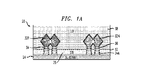
[0013] FIG. lA is a schematic, cross-sectional view taken along line X of FIG.
1 showing
further elements of the monolithic semiconductor structure;
[0014] FIG. 1B is a schematic, cross-sectional view taken along line Y of FIG.
1 showing
further elements of the monolithic semiconductor structure;
4
CA 03192555 2023- 3- 13
WO 2022/127344
PCT/CN2021/124804
[0015] FIG. 2A is a schematic, cross-sectional view of the structure shown in
FIG. 1 A
following a selective oxide etch;
[0016] FIG. 2B is a schematic, cross-sectional view of the structure shown in
FIG. 1B
following the selective oxide etch;
[0017] FIG. 3A is a schematic, cross-sectional view of the structure as shown
in FIG. 2A
following removal of a contact etching stop layer (CESL);
[0018] FIG. 3B is a schematic, cross-sectional view of the structure as shown
in FIG. 2B
following removal of a contact etching stop layer (CESL);
[0019] FIG. 4A is a schematic, cross-sectional view of the structure as shown
in FIG. 3A
following formation of a suicide liner around source/drain regions thereof;
[0020] FIG. 4B is a schematic, cross-sectional view of the structure as shown
in FIG. 3B
following deposition of a metal liner;
[0021] FIG. 5A is a schematic, cross-sectional view of the structure as shown
in FIG. 4A
following deposition and patterning of a block mask thereon;
[0022] FIG. 5B is a schematic, cross-sectional view of the structure as shown
in FIG. 4B
following deposition and patterning of a block mask thereon;
[0023] FIG. 6A is a schematic, cross-sectional view of the structure as shown
in FIG. 5A
following selective removal of the metal liner in between active regions
thereof;
[0024] FIG. 6B is a schematic, cross-sectional view of the structure as shown
in FIG. 5B
following selective removal of the metal liner in between active regions
thereof;
[0025] FIG. 7A is a schematic, cross-sectional view of the structure as shown
in FIG. 7A
following removal of the patterned block mask;
[0026] FIG. 7B is a schematic, cross-sectional view of the structure as shown
in FIG. 6B
following removal of the patterned block mask;
[0027] FIG. 8A is a schematic, cross-sectional view of the structure as shown
in FIG. 7A
following deposition of the organic planarization layer (OPL) and partial etch-
back thereof;
[0028] FIG. 8B is a schematic, cross-sectional view of the structure as shown
in FIG. 7B
following deposition of the organic planarization layer (OPL) and partial etch-
back thereof;
CA 03192555 2023- 3- 13
WO 2022/127344
PCT/CN2021/124804
[0029] FIG. 9A is a schematic, cross-sectional view of the structure as shown
in FIG. 8A
following selective chamfering of the metal liner on the gates thereof;
[0030] FIG. 9B is a schematic, cross-sectional view of the structure as shown
in FIG. 8B
following selective chamfering of the metal liner on the gates thereof;
[0031] FIG. 10A is a schematic, cross-sectional view of the structure as shown
in FIG. 9A
following removal of the OPL;
[0032] FIG. 10B is a schematic, cross-sectional view of the structure as shown
in FIG. 9B
following removal of the OPL;
[0033] FIG. 11A is a schematic, cross-sectional view of the structure as shown
in FIG. 10A
following deposition and planarization of an interlevel dielectric (ILD) layer
thereon;
[0034] FIG. 11B is a schematic, cross-sectional view of the structure as shown
in FIG. 10B
following deposition and planarization of an ILD layer thereon;
[0035] FIG. 12A is a schematic, cross-sectional view of the structure as shown
in FIG. 11A
following contact trench formation in the ILD layer;
[0036] FIG. 12B is a schematic, cross-sectional view of the structure as shown
in FIG. 11B
following contact trench formation in the ILD layer;
[0037] FIG. 13A is a schematic, cross-sectional view of the structure as shown
in FIG. 12A
following contact metallization;
[0038] FIG. 13B is a schematic, cross-sectional view of the structure as shown
in FIG. 12B
following contact metallization;
[0039] FIG. 14A is a schematic, cross-sectional view of the structure as shown
in FIG. 13A
following planarization; and
[0040] FIG. 14B is a schematic, cross-sectional view of the structure as shown
in FIG. 13B
following planarization.
[0041] It is to be appreciated that elements in the figures are illustrated
for simplicity and
clarity. Common but well-understood elements that may be useful or necessary
in a
commercially feasible embodiment may not be shown in order to facilitate a
less hindered
view of the illustrated embodiments.
6
CA 03192555 2023- 3- 13
WO 2022/127344
PCT/CN2021/124804
DETAILED DESCRIPTION
[0042] Principles of the present invention will be described herein in the
context of
illustrative embodiments. It is to be appreciated, however, that the specific
embodiments
and/or methods illustratively shown and described herein are to be considered
exemplary as
opposed to limiting. Moreover, it will become apparent to those skilled in the
art given the
teachings herein that numerous modifications can be made to the embodiments
shown that
are within the scope of the claims. That is, no limitations with respect to
the embodiments
shown and described herein are intended or should be inferred.
[0043] An exemplary sequence of steps that may be employed for forming wrap-
around
contacts (WACs) is shown in the figures. While the disclosed method and the
resulting
structure relate to GAA nanosheet architectures, the principles of the
inventions can also be
applied to other 1-i'ET architectures such as FinFETs.
[0044] An exemplary monolithic structure 20 as shown in FIGS. 1, lA and 1B may
be
obtained during a fabrication process in which GAA nanosheet architectures are
provided.
Various techniques are known to the art for fabricating such architectures and
similar
architectures and new techniques continue to be developed. The exemplary
structure 20
includes pFETs and nFETs, each including a stack of alternating semiconductor
channel
layers 21 (shown in cross-section in FIG. 1B). The semiconductor channel
layers 21 may be,
for example, silicon nanosheets. The nanosheets can be formed on a
semiconductor-on-
insulator substrate or on a bulk semiconductor substrate such as a bulk
silicon substrate.
Shallow trench isolation (STI) regions 26 formed within the substrate 24
provide electrical
isolation of active regions including neighboring transistors or other devices
that may be
formed on the substrate. In an exemplary embodiment, the active regions 24A of
the substrate
24 comprise monocrystalline silicon fins, though impurities may be present
within the
crystalline structure. Single crystal silicon wafers are commercially
available and are
characterized by a diamond cube lattice structure. As known in the art, the
Miller indices of a
substrate are determined from the reciprocals of the points at which the
crystal plane of
silicon intersects the principal crystalline axes. Exemplary embodiments as
described herein
relate to structures including doped or undoped (100) silicon as a substrate
material.
[0045] In one or more exemplary embodiments, the semiconductor channel layers
21 each
have a thickness in the range of four to ten nanometers (4-10nm). The number
of
7
CA 03192555 2023- 3- 13
WO 2022/127344
PCT/CN2021/124804
semiconductor (channel) layers in the semiconductor layer stack may vary
depending on the
desired uses and capabilities of the nanosheet transistors to be fabricated.
The channel layers
21 may consist essentially of monocrystalline silicon layers, possibly
including impurities,
and are spaced six to twenty nanometers (6-20 nm) apart in some embodiments.
The width of
each semiconductor channel layer 21 is about twenty to fifty nanometers (20-50
nm) in some
embodiments, though this range should be considered exemplary as opposed to
restrictive.
[0046] Fabrication of the structure 20 may include replacing sacrificial
silicon germanium
layers (not shown) between the channel layers 21 by metal gate and gate
dielectric materials
that form gate-all-around structures (gate stacks) 28 as schematically
illustrated in FIGS. 1
and 1B. Silicon and silicon germanium layers can be epitaxially grown in
alternating
sequence to obtain a vertical stack having the desired number of silicon
(channel) layers. The
terms "epitaxially growing and/or depositing" and "epitaxially grown and/or
deposited" mean
the growth of a semiconductor material on a deposition surface of a
semiconductor material
in which the semiconductor material being grown has the same crystalline
characteristics as
the semiconductor material of the deposition surface. In an epitaxial
deposition process, the
chemical reactants provided by the source gases are controlled and the system
parameters are
set so that the depositing atoms arrive at the deposition surface of the
semiconductor substrate
with sufficient energy to move around on the surface and orient themselves to
the crystal
arrangement of the atoms of the deposition surface. Therefore, an epitaxial
semiconductor
material has the same crystalline characteristics as the deposition surface on
which it is
formed.
[0047] The gate structures 28 may have a thickness in the range of six to
twenty nanometers
(6-20 nm). The dimension ranges of the channel layers and gate structures
should be
considered exemplary as opposed to limiting. A gate dielectric layer forms
portions of the
gate stacks 28 that replace the sacrificial silicon germanium layers. The gate
stacks adjoin the
silicon nanoshcct channel layers 21 and extend down to a bottom dielectric
isolation (BDI)
layer 36 and/or the ST1 region 26. Non-limiting examples of suitable materials
for the gate
dielectric layer include oxides, nitrides, oxynitrides, silicates (e.g., metal
silicates),
aluminates, titanates, nitridcs, or any combination thereof. Examples of high-
k gate dielectric
materials (with a dielectric constant greater than 7.0) include, but are not
limited to, metal
oxides such as hafnium oxide, hafnium silicon oxide, hafnium silicon
oxynitridc, lanthanum
oxide, lanthanum aluminum oxide, zirconium oxide, zirconium silicon oxide,
zirconium
silicon oxynitride, tantalum oxide, titanium oxide, barium strontium titanium
oxide, barium
8
CA 03192555 2023- 3- 13
WO 2022/127344
PCT/CN2021/124804
titanium oxide, strontium titanium oxide, yttrium oxide, aluminum oxide, lead
scandium
tantalum oxide, and lead zinc niobate. The high-k material may further include
dopants such
as, for example, lanthanum and aluminum.
[0048] The gate dielectric layer may be formed by suitable deposition
processes, for example,
chemical vapor deposition (CVD), plasma-enhanced chemical vapor deposition
(PECVD),
atomic layer deposition (ALD), evaporation, physical vapor deposition (PVD),
chemical
solution deposition, or other like processes. The thickness of the gate
dielectric material may
vary depending on the deposition process as well as the composition and number
of high-k
dielectric materials used. In one exemplary embodiment, a high-k dielectric
layer having a
thickness of 2.5 nm is employed. In some embodiments, the gate dielectric
layer incudes
multiple layers.
[0049] Source/drain regions 32P, 32N are epitaxially grown on the exposed
edges of the
silicon (channel) layers 21 and may be merged. The source/drain regions are
electrically
isolated from the substrate 24 by the bottom dielectric isolation (BD1) layer
36. Dopants
within the source/drain regions 32 may be incorporated in situ using
appropriate precursors,
as known in the art. By "in-situ" it is meant that the dopant that dictates
the conductivity type
of a doped layer is introduced during the process step, for example epitaxial
deposition, that
forms the doped layer. As used herein, the term "conductivity type" denotes a
dopant region
being p-type or n-type. As used herein, "p-type" refers to the addition of
impurities to an
intrinsic semiconductor that creates deficiencies of valence electrons. In a
silicon-containing
substrate, examples of p-type dopants, i.e., impurities include but are not
limited to: boron,
aluminum, gallium and indium. As used herein, "n-type' refers to the addition
of impurities
that contribute free electrons to an intrinsic semiconductor. In a silicon-
containing substrate,
examples of n-type dopants, i.e., impurities, include but are not limited to
antimony, arsenic
and phosphorous. Exemplary cpitaxial growth processes that arc suitable for
use in forming
silicon and/or silicon germanium cpitaxy include rapid thermal chemical vapor
deposition
(RTCVD), low-energy plasma deposition (LEPD), ultra-high vacuum chemical vapor
deposition (UHVCVD), atmospheric pressure chemical vapor deposition (APCVD)
and
molecular beam epitaxy (MBE). An nFET region(s) includes transistors having n-
type
source/drain regions while the pFET region(s) includes p-type source/drain
regions. The use
of a BDI layer 36 is optional to the fabrication of nFET and pFET transistors
as described
herein.
9
CA 03192555 2023- 3- 13
WO 2022/127344
PCT/CN2021/124804
[0050] The monolithic structure 20 further includes a contact etching stop
layer (CESL) that
is formed as a liner thereon subsequent to source/drain epitaxy. The CESL
liner 37 is formed,
in some embodiments, by depositing a conformal layer of silicon nitride, low-k
dielectric
materials such as silicon-carbon-boron-nitrogen (SiCBN), silicon oxycarbide
(Si0C) or
silicon-carbon-oxynitride (SiCON), over and between source-drain regions 32P,
32N.
[0051] Next, an interlayer dielectric (ILD) 38, for example silicon dioxide
(SiO2) or any
other material with similar functional properties, is formed by chemical vapor
deposition
(CVD) or any other suitable deposition technique, over the source-drain
regions and the
CESL liner 37. The structure 20 further includes dielectric gate sidewall
spacers 42 and gate
caps 44, as shown in FIG. 1B. Techniques for forming such spacers and gate
caps are known
to the art. The CESL liner 37 also extends over the gate sidewall spacers and
the gate caps.
Following planarization of the gate cap layer from which the gate caps are
formed and
deposition of an oxide fill, the elements discussed above are embedded within
the ILD layer
38 as shown in FIGS. lA and 1B.
[0052] Referring to FIGS. 2A and 2B, the ILD layer 38 is selectively removed
using, for
example, a wet hydrofluoric (HF) acid etch or any other suitable etch. The
CESL liner 37 is
then selectively removed to obtain a structure 30 as schematically illustrated
in cross-section
in FIG. 3A and FIG. 3B. A wet phosphoric acid etch or other suitable etch may
be employed
to selectively remove the CESL liner 37 in one or more embodiments.
[0053] A TS liner wrapping around the source/drain regions 32P, 32N may be
foimed by
conformal deposition of a titanium (Ti) liner 46 or other suitable metal liner
using CVD.
Deposition of the liner 46 may be followed by an annealing step at this stage
of the process or
later to form titanium silicide and/or titanium-based germano-silicide layers
on the
source/drain regions. A conformal film is understood as having substantially
uniform
thickness. In some exemplary structures including both nFET and pFET regions,
annealing
causes the source/drain regions within the nFET region to include TiS2 layers
while titanium
germano-silicide (Ti(SiGe)?) layers are formed on the source/drain regions in
the pFET
region. The terms titanium silicide and metal silicide as used hereafter are
intended to
encompass silicides formed on either silicon or silicon germanium. The
thickness of the Ti
liner 46 may, for example, be in the range of two to five nanometers (2 nm to
5 nm). The
liner further extends over the STI region 26, the gate sidewall spacers 42,
and the gate caps
44 as illustrated in FIGS. 4A and 4B. A structure 40 is thereby obtained.
CA 03192555 2023- 3- 13
WO 2022/127344
PCT/CN2021/124804
[0054] An organic planarization layer (OPL) 48 is deposited on the structure
40 and
patterned to form a block mask. In accordance with an embodiment of the
present invention,
the OPL 48 may be an organic polymer including carbon, hydrogen and nitrogen.
Non-
limiting examples of the OPL material include JSR HM8006, JSR HM8014, AZ
UM10M2,
Shin Etsu ODL 102, or other similar commercially available materials from such
vendors as
JSR, TOK, Sumitomo, and Rohm & Haas. The OPL 48 can be deposited, for example,
by
spin coating and excess material is etched back. As shown in FIGS. 5A and 5B,
the
remaining portions of the OPL form a block mask that extends over and protects
the active
regions 24A of the substrate 24. The source/drain regions 32P, 32N, the
portions of the liner
46 wrapping around the source/drain regions, and the gate structures on the
active regions are
embedded within the patterned OPL and therefore protected. The patterned OPL
extends over
as well as laterally beyond the source/drain regions, as shown in FIG. 5A,
while leaving a
horizontal portion of the titanium liner 46 between the pFET and nFET active
regions
exposed. The portions of the titanium liner 46 extending over the STI region
26 and gate
structures 28 located between the active regions are exposed following OPL
patterning in the
resulting structure 50.
[0055] The exposed portions of the titanium liner 46 between active regions
24A are
selectively removed. The selective removal of titanium-based material may be
conducted by
a wet process using, for example, sulfuric peroxide mixture (SPM), which
combines the use
of sulfuric acid and hydrogen peroxide. As used herein, the term "selective"
in reference to a
material removal process (e.g., etching) denotes that, with an appropriate
etchant choice, the
material removal rate (i.e., etch rate) for the targeted material is greater
than the removal rate
for at least another material exposed to the material removal process and
preferably much
greater. A structure 60 as schematically illustrated in cross-section in FIGS.
6A and 6B may
accordingly be obtained. Removal of the OPL 48 from the structure 60 re-
exposes titanium-
covered source/drain regions 32P, 32N and other structures above the active
regions 24A of
the substrate 24. A structure 70 as schematically illustrated in FIGS. 7A and
7B may be
obtained. As shown in FIG. 7A, the metal liner 46 now includes horizontal
segments 46A
extending partially over the STI region 26 and laterally beyond the lateral
end portions of the
source/drain regions directly above them.
[0056] A further organic planarization layer 48' is deposited and etched back
to obtain a
structure 80 as schematically illustrated in FIGS. 8A and 8B. The OPL 48' may,
but does not
necessarily comprise the same materials as the OPL 48 discussed above. It may
be deposited
11
CA 03192555 2023- 3- 13
WO 2022/127344
PCT/CN2021/124804
in the same manner or using a different technique. As shown in FIG. 8A and 8B,
the
thickness of the OPL 48' is sufficient that the source/drain regions 32P, 32N,
including the
titanium (silicide) layer 48 thereon, are embedded within the OPL and are
therefore protected.
Portions of the gate structures 28 and the gate sidewall spacers 42 extend
above the top
surface of the OPL. The titanium-covered gate caps 44 formed over the active
regions 24A
are entirely exposed. By providing sufficient uniformity of the recessed OPL
48' below the
top surfaces of the gate caps 44 across a wafer on which the field-effect
transistors are formed,
the portions of the titanium layer 46 on the gate caps 44 are entirely exposed
while none of
the titanium (or silicide) on the epitaxial source/drain regions 32P, 32N is
exposed.
[0057] Selective titanium chamfering causes removal of the exposed portions of
the titanium
liner 46 above the top surface of the OPL 48'. As discussed above, the
selective removal of
titanium-based material may be conducted by a wet process using, for example,
sulfuric
peroxide mixture (SPM). A structure 90 as schematically illustrated in cross-
section in FIGS.
9A and 9B may accordingly be obtained. The remaining vertical portions 46B of
the titanium
liner adjoin the gate sidewall spacers 42 and terminate below the gate caps
44. The gate
structures 28, having top end portions adjoining the gate caps 44, extend
above the vertical
portions 46B of the titanium layer 46.
[0058] The second OPL 48' may be removed by ashing or other suitable process
to obtain a
structure 100 as schematically illustrated in cross-section in FIGS. 10A and
10B. The liner 46
now comprises a plurality of discrete, contiguous segments, each segment
including a metal
silicide portion and metal portions extending from the silicide portion. As
shown in FIG. 10A,
the titanium silicide portions of the liner 46 wrap around the source/drain
regions 32P, 32N.
Laterally extending metal (non-silicide) portions 46A of the liner 46 extend a
limited distance
horizontally from sub-fin regions below the bottom dielectric isolation layer
36 and over
portions of the STI region 26. As discussed above, the laterally extending
portions 46A of the
liner 46 segments further extend laterally beyond the source/drain regions
32P, 32N of the
associated field-effect transistors. Vertical portions 46B of the titanium
liner 46 segments are
localized between pairs of the gate structures 28, as illustrated in FIG. 10B.
Each vertical
portion 46B includes a pair of metal segments adjoining gate sidewall spacers
42. The
vertical portions 46B are located entirely beneath the top surfaces of the
gate structures 28
and the gate caps 44.
[0059] An interlevel dielectric (ILD) layer 52 is deposited on the structure
90 and planarized.
The ILD layer may be deposited using, for example, deposition techniques
including, but not
12
CA 03192555 2023- 3- 13
WO 2022/127344
PCT/CN2021/124804
necessarily limited to, chemical vapor deposition (CVD), plasma enhanced CVD
(PECVD),
radio-frequency CVD (RFCVD), physical vapor deposition (PVD), atomic layer
deposition
(ALD), molecular beam deposition (MBD), pulsed laser deposition (PLD), and/or
liquid
source misted chemical deposition (LSMCD), spin-on coating, sputtering, and/or
plating. The
ILD layer 52 may include, but is not limited to, low-k materials (e.g., k less
than about 4.0),
such as, for example, porous silicates, carbon doped oxides, silicon dioxides,
silicon
oxynitrides, carbon-doped silicon oxide (SiCOH) and porous variants thereof,
silsesquioxanes, siloxanes, or other dielectric materials having, for example,
a dielectric
constant in the range of about 2 to about 4.
[0060] The interlevel dielectric (ILD) layer 52 is confat
__________________________ mally deposited on the structure 90,
thereby filling the spaces between the elements comprising the nFETs and pFETs
above the
substrate 24. The interlevel dielectric layer may, for example, comprise a
conformal oxide
such as ALD silicon dioxide in one exemplary embodiment. Flowable ILD
materials may be
employed in one or more embodiments. A substantially carbon free silicon oxide
(SiO2)
material can, for example, be deposited using FCVD. Flowable chemical vapor
deposition
(FCVD) provides for a liquid-like film that flows freely into trench-like
geometries to
provide a bottom up, void-free and seam-free fill. Other dielectric materials
may alternatively
be employed in some embodiments, though etch selectivity between the ILD layer
52 and the
gate sidewall spacers 42, the gate caps 44 and the metal silicide should be
provided. The ILD
layer 52 can be optionally cured using various known curing techniques
including UV-light-
assisted cure at below 400 C. The resulting structure is then subjected to
chemical
mechanical planarization (CMP). A structure 110 as schematically illustrated
in FIGS. 11A
and 11B can thereby be obtained wherein the horizontal portions 46A of the
metal liner 46
are localized between the ILD layer 52 and the STI region 26.
[0061] Trench openings are conventionally formed in an ILD layer 52 by using,
for example,
known damascene techniques. Photolithography and etching steps follow ILD
layer
deposition. Specifically, a photoresist (not shown) is applied over the 1LD
layer. The
photoresist can be applied by any suitable technique, including, but not
limited to coating or
spin-on techniques. A mask (not shown), which is patterned with shapes
defining trench
openings and/or contact holes to be formed, is provided over the photoresist,
and the mask
pattern is transferred to the photorcsist using a photolithographic process,
which creates
recesses in the uncovered regions of the photoresist. The patterned
photoresist is
subsequently used to create the same pattern of recesses in the ILD dielectric
layer through
13
CA 03192555 2023- 3- 13
WO 2022/127344
PCT/CN2021/124804
conventional etching typically used for forming trenches and contact holes. A
dry etch (for
example, a reactive ion etch) may he employed to form such trenches and
contact holes. The
etching selectively removes a portion of the ILD layer 52. After formation of
the trench
openings 54, the photoresist may be stripped by ashing or other suitable
process from the ILD
layer. The resulting structure 120, as schematically illustrated in FIGS. 12A
and 12B, may he
subjected to a wet clean.
[0062] After the resist is stripped, the trench (via) openings are cleaned and
then lined with,
for example, a thin PVD (e.g. sputtered) titanium (Ti) layer (not shown). The
Ti film serves
as an adhesion layer and also decreases contact resistance to underlying
conductors by
reducing interfacial oxides. Titanium nitride (TiN) (not shown) is
subsequently deposited
either by sputtering or by CVD. A contact metal layer 56, for example tungsten
(W) or cobalt
(Co), is conformally deposited on the structure, filling the trenches 54
formed the ILD layer
52 and directly contacting the metal silicide and/or metal germano-silicide
layers formed on
the source/drain regions 32N, 32P from the metal liner 46. The vertically
extending portions
46B of the liner are also in contact with the metal contact layer 56, as shown
in FIG. 13B. In
some embodiments, the contact metal layer is a tungsten (W) layer that is
deposited using a
tungsten hexafluoride source with silane. Chemical vapor deposition conducted
between 300-
400 C and using tungsten hexafluoride precursor chemistry may, for example, be
employed
to deposit a tungsten layer. Contact material may, for example, alternatively
include tantalum
(Ta), aluminum (Al), platinum (Pt), gold (Au), titanium (Ti), palladium (Pd)
or any
combination thereof. The contact material may be deposited by, for example,
CVD, PECVD,
PVD, plating, thermal or e-beam evaporation, or sputtering. A structure 130 as
schematically
illustrated in FIGS. 13A and 13B may be obtained following trench silicide
metallization as
describe above.
[0063] A planarization process such as CMP is performed to remove any
electrically
conductive material (overburden) from the top surface of the structure. The
thickness of the
ILD layer 52 may also be reduced using CMP to obtain a structure 140 as
schematically
illustrated in FIGS. 14A and 14B. As shown in FIG. 14A, metal silicide wraps
around the
source/drain regions 32P, 32N. As shown in FIG. 14B, the metal silicide around
the
source/drain regions and the contiguous portions 46B of the liner 46 extending
above the
source/drain regions arc localized between the gate structures 28. All
remaining portions of
the liner 46 are located beneath the top surfaces of the gate structures 28. A
semiconductor
structure 140 including gate-all-around (GAA) architecture, wrap-around
source/drain
14
CA 03192555 2023- 3- 13
WO 2022/127344
PCT/CN2021/124804
contacts, and localized metal/silicide may be provided. Moreover, the
combination of block
mask patterning and chamfering to fabricate such a structure obviates the need
for inverse
tone patterning.
[0064] The drawing figures as discussed above depict exemplary processing
steps/stages in
the fabrication of exemplary structures. Although the overall fabrication
methods and the
structures formed thereby are entirely novel, certain individual processing
steps required to
implement the method may utilize conventional semiconductor fabrication
techniques and
conventional semiconductor fabrication tooling. These techniques and tooling
will already be
familiar to one having ordinary skill in the relevant arts given the teachings
herein. Moreover,
one or more of the processing steps and tooling used to fabricate
semiconductor devices are
also described in a number of readily available publications, including, for
example James D.
Plummer et al., Silicon VLSI Technology: Fundamentals, Practice, and Modeling
Pr Edition,
Prentice Hall, 2001, which is hereby incorporated by reference herein. It is
emphasized that
while some individual processing steps are set forth herein, those steps are
merely illustrative,
and one skilled in the art may be familiar with several equally suitable
alternatives that would
be applicable.
[0065] It is to be appreciated that the various layers and/or regions shown in
the
accompanying figures may not be drawn to scale. Furthermore, one or more
semiconductor
layers of a type commonly used in such integrated circuit devices or other
layers may not be
explicitly shown in a given figure for ease of explanation. This does not
imply that the
semiconductor layer(s) or other layer(s) not explicitly shown are omitted in
the actual
integrated circuit device.
[0066] Given the discussion thus far, it will be appreciated that, in general
terms, an
exemplary method of forming a semiconductor structure including wrap-around
contacts
includes conformally depositing a metal liner on a monolithic structure that
includes first and
second active regions 24A and field-effect transistors (FETs) on the first and
second active
regions. FIGS. 3A and 3B show an exemplary monolithic structure 30 including
nanosheet
FETs. The FETs include gate structures 28 and epitaxial source/drain regions
32P and/or 32N.
A metal suicide liner is formed on the epitaxial source/drain regions from the
metal liner and
wraps around the source/drain regions. The first and second active regions are
protected with
a patterned block mask 48 as schematically illustrated in FIGS. 5A and 5B. The
metal liner is
selectively removed from a region exposed by the patterned block mask between
the first and
second active regions. A structure 70 as shown in FIGS. 7A and 7B is obtained
following
CA 03192555 2023- 3- 13
WO 2022/127344
PCT/CN2021/124804
removal of the patterned block mask 48. As schematically illustrated in FIGS.
8A and 8B, a
protective mask 48' is formed on the monolithic structure. The protective mask
protects the
epitaxial source/drain regions, which are entirely beneath the top surface of
the protective
mask. Portions of the metal liner 46 above the first and second active regions
are exposed.
The exposed portions of the metal liner 46 above the active regions are
removed followed by
removal of the protective mask 48'. A monolithic semiconductor structure 100
as shown in
FIGS. 10A and 10B may accordingly be obtained, it being appreciated that the
exemplary
method can be applied with respect to nanosheet transistors as shown as well
as other types of
FETs such as FinFETs.
[0067] In an exemplary embodiment, forming the protective mask includes
depositing an
organic planarization layer on the monolithic structure and etching back the
organic
planarization layer to expose the top portions of the gate structures 28 and
associated gate
sidewall spacers 42 and gate caps 44. The method may include forming an
interlevel
dielectric layer 52 on the monolithic structure, patterning the interlevel
dielectric layer,
thereby exposing the metal silicide liner on the epitaxial source/drain
regions 32P, 32N as
shown in FIGS. 12A and 12B, and forming metal contacts 56 within the
interlevel dielectric
layer and directly contacting the metal silicide liner on the epitaxial
source/drain regions.
FIGS. 13A and 13B illustrate an exemplary structure 130 following contact
metallization.
The monolithic structure 30 in one or more exemplary embodiments further
includes gate
caps 44 and gate sidewall spacers 42 adjoining the gate structures, wherein
selectively
removing the metal liner 46 above the top portions of the gate structures
includes removing
the metal liner from the gate caps and portions of the gate sidewall spacers.
The monolithic
structure includes a shallow trench isolation region 26 in one or more
embodiments, wherein
selectively removing the metal liner 46 from a region between the first and
second active
regions includes removing the metal liner from a top surface of the shallow
trench isolation
region 26.
[0068] A semiconductor structure provided in accordance with one or more
embodiments
includes a semiconductor substrate 24 including a first active region 24A and
a second active
region 24A and a shallow trench isolation region 26 between the first active
region and the
second active region. A first field-effect transistor on the first active
region includes a gate
structure 28 on the first active region, a channel region (the region of layer
21 adjoining the
gate structure), and a pair of epitaxial source/drain regions 32P or 32N on
opposite sides of
the channel region. Each epitaxial source/drain region is located between a
pair of gate
16
CA 03192555 2023- 3- 13
WO 2022/127344
PCT/CN2021/124804
structures on the first active region. A wrap-around metal silicide liner (the
silicide portion of
conformal metal layer 46) adjoins each epitaxial source/drain region of the
first field-effect
transistor. A dielectric layer 52 extends over the semiconductor substrate and
the first field-
effect transistor. Metal liner portions are contiguous, respectively, with
each metal silicide
liner. Each metal liner portion includes a vertically extending portion 46B
located between a
pair of the gate structures 28 on the first active region and extending above
the source/drain
regions. The gate structures 28 on the first active region extend vertically
above the vertically
extending portion 46B. A horizontally extending metal liner portion 46A
extends below the
source/drain regions of the first field-effect transistor and is positioned
between the shallow
trench isolation region 26 and the dielectric layer 52. As shown, for example,
in FIG. 14A the
horizontally extending portion 46A of each metal liner portion extends
laterally beyond one
of the source/drain regions of the first field-effect transistor directly
above.
[0069] At least a portion of the techniques described above may be implemented
in an
integrated circuit. In forming integrated circuits, identical dies are
typically fabricated in a
repeated pattern on a surface of a semiconductor wafer. Each die includes a
device described
herein, and may include other structures and/or circuits. The individual dies
are cut or diced
from the wafer, then packaged as an integrated circuit. One skilled in the art
would know how
to dice wafers and package die to produce integrated circuits.
[0070] Those skilled in the art will appreciate that the exemplary structures
discussed above
can be distributed in raw form (i.e., a single wafer having multiple
unpackaged chips), as bare
dies, in packaged form, or incorporated as parts of intermediate products or
end products that
benefit from having nanosheet or other FET devices having wrap-around contacts
formed in
accordance with one or more of the exemplary embodiments.
[0071] There are numerous techniques used by those skilled in the art to
remove material at
various stages of creating a semiconductor structure. As used herein, these
processes are
referred to generically as "etching". For example, etching includes techniques
of wet etching,
dry etching, chemical oxide removal (COR) etching, and reactive ion etching
(RIE), which
are all known techniques to remove select material when forming a
semiconductor structure.
The Standard Clean 1 (SC1) contains a strong base, typically ammonium
hydroxide, and
hydrogen peroxide. The SC2 contains a strong acid such as hydrochloric acid
and hydrogen
peroxide. The techniques and application of etching is well understood by
those skilled in the
art and, as such, a more detailed description of such processes is not
presented herein.
17
CA 03192555 2023- 3- 13
WO 2022/127344
PCT/CN2021/124804
[0072] The illustrations of embodiments described herein are intended to
provide a general
understanding of the various embodiments, and they are not intended to serve
as a complete
description of all the elements and features of apparatus and systems that
might make use of
the circuits and techniques described herein. Many other embodiments will
become apparent
to those skilled in the art given the teachings herein; other embodiments are
utilized and
derived therefrom, such that structural and logical substitutions and changes
can he made
without departing from the scope of this invention. It should also be noted
that, in some
alternative implementations, some of the steps of the exemplary methods may
occur out of
the order noted in the figures. For example, two steps shown in succession
may, in fact, he
executed substantially concurrently, or certain steps may sometimes be
executed in the
reverse order, depending upon the functionality involved. The drawings are
also merely
representational and are not drawn to scale. Accordingly, the specification
and drawings are
to be regarded in an illustrative rather than a restrictive sense.
[0073] Embodiments may be referred to herein, individually and/or
collectively, by the term
"embodiment" merely for convenience and without intending to limit the scope
of this
application to any single embodiment or inventive concept if more than one is,
in fact, shown.
Thus, although specific embodiments have been illustrated and described
herein, it should be
understood that an arrangement achieving the same purpose can be substituted
for the
specific embodiment(s) shown. Combinations of the above embodiments, and other
embodiments not specifically described herein, will become apparent to those
of skill in the
art given the teachings herein.
[0074] The terminology used herein is for the purpose of describing particular
embodiments
only and is not intended to be limiting. As used herein, the singular forms -
a," -an" and "the"
are intended to include the plural forms as well, unless the context clearly
indicates otherwise.
It will be further understood that the terms "comprises" and/or "comprising,"
when used in
this specification, specify the presence of stated features, steps,
operations, elements, and/or
components, but do not preclude the presence or addition of one or more other
features, steps,
operations, elements, components, and/or groups thereof Terms such as "above"
and "below"
and "vertical" arc used to indicate relative positioning of elements or
structures to each other
as opposed to relative elevation.
[0075] The corresponding structures, materials, acts, and equivalents of any
means or step-
plus-function elements in the claims below are intended to include any
structure, material, or
act for performing the function in combination with other claimed elements as
specifically
18
CA 03192555 2023- 3- 13
WO 2022/127344
PCT/CN2021/124804
claimed. The description of the various embodiments has been presented for
purposes of
illustration and description, but is not intended to be exhaustive or limited
to the forms
disclosed. Many modifications and variations will be apparent to those of
ordinary skill in
the art without departing from the scope thereof. The embodiments were chosen
and
described in order to best explain principles and practical applications, and
to enable others of
ordinary skill in the art to understand the various embodiments with various
modifications as
are suited to the particular use contemplated.
[0076] The abstract is provided to comply with 37 C.F.R. 1.72(b). It is
submitted with the
understanding that it will not be used to interpret or limit the scope or
meaning of the claims.
In addition, in the foregoing Detailed Description, it can be seen that
various features are
grouped together in a single embodiment for the purpose of streamlining the
disclosure. This
method of disclosure is not to be interpreted as reflecting an intention that
the claimed
embodiments require more features than are expressly recited in each claim.
Rather, as the
appended claims reflect, the claimed subject matter may lie in less than all
features of a single
embodiment. Thus, the following claims are hereby incorporated into the
Detailed
Description, with each claim standing on its own as separately claimed subject
matter.
[0077] Given the teachings provided herein, one of ordinary skill in the art
will be able to
contemplate other implementations and applications of the techniques and
disclosed
embodiments. Although illustrative embodiments have been described herein with
reference
to the accompanying drawings, it is to be understood that illustrative
embodiments are not
limited to those precise embodiments, and that various other changes and
modifications are
made therein by one skilled in the art without departing from the scope of the
appended
claims.
19
CA 03192555 2023- 3- 13