Note: Descriptions are shown in the official language in which they were submitted.
WO 2022/070104
PCT/1B2021/058950
METHOD AND SYS IBM FOR CLEANING A FIELD EMISSION CATHODE DEVICE
BACKGROUND
Field of the Disclosure
The present application relates to field emission cathode devices and, more
particularly, to a method
and system for cleaning a field emission cathode device.
Description of Related Art
A field emission cathode device generally includes a cathode substrate
(usually comprised of a
metal or other conducting material such as stainless steel, tungsten,
molybdenum, doped silicon), a layer of a
field emission material (e.g., nanotubes, nanowires, graphene, amorphous
carbon) disposed on the substrate,
and, if necessary, an additional layer of an adhesion material disposed
between the substrate and the field
emission material (see, e.g., FIG. 1). Some typical applications of a field
emission cathode device include,
for example, electronics operable in a vacuum environment, field emission
displays, and X-ray tubes. in
some such applications, the field emission cathode device(s) must be clean or
be thoroughly cleaned in order
to be used effectively in ultra-clean and/or high vacuum environments.
With field emission materials and adhesion materials deposited on a surface of
the cathode substrate,
however, it may be difficult to clean the field emission cathode device prior
to or after use. The surface
deposition (field emission) material typically includes a mixture of
nanomatcrials (e.g., nanotubcs, graphcnc,
nanowires, etc.) and adhesive materials (e.g., glass particles, metal
particles, etc.). Even after cleaning the
field emission cathode device using standard cleaning processes (e.g., blowing
the field emission material
surface with dry air, contacting the field emission material surface with
adhesive tape and then removing the
tape, etc.), the field emission material surface is still capable of releasing
small loose particles (e.g., particles
that are not securely embedded in or adhered to the field emission material
and/or the adhesive layer)
through actual operation or even just over time. Such dislodged particles lead
to contamination of the
vacuum environment, causing, for example, electrical arcing and electrode
short-circuiting within the
vacuum environment. Generally, a source of loose particles in the context of
such field emission cathode
devices includes lack of adhesion of some of the surface deposition / field
emission material to the adhesive
layer or to the substrate itself, which may cause the non-embedded particles
to work loose during device
operation. Also, the cathode surface (e.g., the field emission material layer)
is generally not smooth, and
includes uneven surface morphology, such as peaks, valleys, and caves (see,
e.g., FIG. 1), which can trap
and hold non-embedded particles that are not readily or completely removed by
standard cleaning
procedures.
Thus, there exists a need for a method and system for effectively cleaning a
field emission cathode
device so as to desirably- remove particles that are not securely embedded in
or adhered to the cathode
surface, wherein such improvements would minimize or eliminate electrical
arcing and/or electrode short-
circuiting within the vacuum environment.
1
CA 03194247 2023- 3- 29
WO 2022/070104
PCT/IB2021/058950
SUMMARY OF THE DISCLOSURE
The above and other needs are met by aspects of the present disclosure which
includes, without
limitation, the following example embodiments and, in one particular aspect,
provides a method of cleaning
a field emission cathode device, wherein the field emission cathode device
includes a substrate having a
field emission layer engaged therewith. Such a method comprises engaging the
field emission cathode
device with a vibration device such that the substrate is disposed above the
field emission layer (e.g., such
that the cathode, namely the field emission layer deposited on the substrate,
is "upside down"); and vibrating
the field emission cathode device with the vibration device in an X, Y, or Z
direction at a predetermined
frequency and at a predetermined amplitude for a predetermined time duration
so as to clean the field
emission cathode device by dislodging non-embedded particles from the field
emission layer.
Another example aspect provides a system for cleaning a field emission cathode
device, wherein the
field emission cathode device including a substrate having a field emission
layer engaged therewith. Such a
system comprises a vibration device arranged to receive the field emission
cathode device such that the
substrate is disposed above the field emission layer (e.g., such that the
cathode, namely the field emission
layer deposited on the substrate, is "upside down"). The vibration device is
further arranged to vibrate the
field emission cathode device in an X, Y, or Z direction at a predetermined
frequency and at a predetermined
amplitude for a predetermined time duration so as to clean the field emission
cathode device by dislodging
non-embedded particles from the field emission layer.
The present disclosure thus includes, without limitation, the following
example embodiments:
Example Embodiment 1: A method of cleaning a field emission cathode device,
the field emission
cathode device including a substrate having a field emission layer engaged
therewith, said method
comprising engaging the field emission cathode device with a vibration device
such that the substrate is
disposed above the field emission layer; and vibrating the field emission
cathode device with the vibration
device in an X, Y, or Z direction at a predetermined frequency and at a
predetermined amplitude for a
predetermined time duration so as to clean the field emission cathode device
by dislodging non-embedded
particles from the field emission layer.
Example Embodiment 2: The method of any preceding example embodiment, or
combinations
thereof, comprising directing a pressurized airstream toward the field
emission layer in association with
vibrating the field emission cathode device.
Example Embodiment 3: The method of any preceding example embodiment, or
combinations
thereof, comprising removing electrostatic charges from the field emission
layer, the electrostatic charges
normally retaining the non-embedded particles in engagement with the field
emission layer, in association
with vibrating the field emission cathode device.
Example Embodiment 4: The method of any preceding example embodiment, or
combinations
thereof, comprising applying a voltage of at least about 1 kV to an electrode
disposed adjacent to and in
spaced apart relation with the field emission layer, in association with
vibrating the field emission cathode
2
CA 03194247 2023- 3- 29
WO 2022/070104
PCT/IB2021/058950
device, an electric field generated by the electrode attracting the non-
embedded particles from the field
emission layer.
Example Embodiment 5: The method of any preceding example embodiment, or
combinations
thereof, wherein vibrating the field emission cathode device comprises
vibrating the field emission cathode
device in the X, Y, or Z direction at the predetermined frequency of between
about 1 Hz and about 1 kHz
and at the predetermined amplitude of between about 1 mm and about 1 cm for
the predetermined time
duration of between about 1 minute and about 10 hours.
Example Embodiment 6: A system for cleaning a field emission cathode device,
the field emission
cathode device including a substrate having a field emission layer engaged
therewith, said system
comprising a vibration device arranged to receive the field emission cathode
device such that the substrate is
disposed above the field emission layer, the vibration device being further
arranged to vibrate the field
emission cathode device in an X, Y, or Z direction at a predetermined
frequency and at a predetermined
amplitude for a predetermined time duration so as to clean the field emission
cathode device by dislodging
non-embedded particles from the field emission laver.
Example Embodiment 7: The system of any preceding example embodiment, or
combinations
thereof, comprising an air emission device arranged adjacent to the vibration
device to direct a pressurized
airstream toward the field emission layer in association with the vibration
device vibrating the field emission
cathode device.
Example Embodiment 8: The system of any preceding example embodiment, or
combinations
thereof, comprising an ionizer or an electrostatic elimination device disposed
adjacent to the vibration device
and arranged to remove electrostatic charges from the field emission layer,
the electrostatic charges normally
retaining the non-embedded particles in engagement with the field emission
layer, in association with the
vibration device vibrating the field emission cathode device.
Example Embodiment 9: The system of any preceding example embodiment, or
combinations
thereof, comprising an electrode disposed adjacent to the vibration device in
spaced apart relation with the
field emission layer; and a voltage source arranged to apply a voltage of at
least about 1 kV to the electrode
in association with the vibration device vibrating the field emission cathode
device, an electric field
generated by the electrode attracting the non-embedded particles from the
field emission layer.
Example Embodiment 10: The system of any preceding example embodiment, or
combinations
thereof, wherein the vibration device is arranged to vibrate the field
emission cathode device in the X, Y, or
Z direction at the predetermined frequency of between about 1 Hz and about 1
kHz and at the predetermined
amplitude of between about 1 mm and about 1 cm for the predetermined time
duration of between about 1
minute and about 10 hours.
These and other features, aspects, and advantages of the present disclosure
will be apparent from a
reading of the following detailed description together with the accompanying
drawings, which are briefly
described below. The present disclosure includes any combination of two,
three, four, or more features or
elements set forth in this disclosure, regardless of whether such features or
elements are expressly combined
3
CA 03194247 2023- 3- 29
WO 2022/070104
PCT/IB2021/058950
or otherwise recited in a specific embodiment description herein. This
disclosure is intended to be read
holistically such that any separable features or elements of the disclosure,
in any of its aspects and
embodiments, should be viewed as intended, namely to be combinable, unless the
context of the disclosure
clearly dictates otherwise.
It will be appreciated that the summary herein is provided merely for purposes
of summarizing some
example aspects so as to provide a basic understanding of the disclosure. As
such, it will be appreciated that
the above described example aspects are merely examples and should not be
construed to narrow the scope
or spirit of the disclosure in any way. it will be appreciated that the scope
of the disclosure encompasses
many potential aspects, some of which will be further described below, in
addition to those herein
summarized. Further, other aspects and advantages of such aspects disclosed
herein will become apparent
from the following detailed description taken in conjunction with the
accompanying drawings which
illustrate, by way of example, the principles of the described aspects.
BRIEF DESCRIPTION OF THE SEVERAL VIEWS OF THE DRAWING(S)
Having thus described the disclosure in general terms, reference will now be
made to the
accompanying drawings, which are not necessarily drawn to scale, and wherein:
FIG. 1 schematically illustrates an example of a field emission cathode device
and the nature of the
field emission material deposition layer engaged with the cathode substrate;
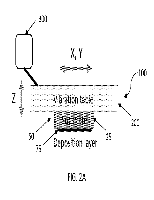
FIG. 2A schematically illustrates a side view of a vibration device for
receiving and cleaning a field
emission cathode device, according to one aspect of the present disclosure;
FIG. 2B schematically illustrates a bottom plan view of a vibration device for
receiving and cleaning
a field emission cathode device, according to the aspect of the present
disclosure shown in FIG. 2A;
FIG. 3 schematically illustrates a side view of a system for receiving and
cleaning a field emission
cathode device, according to one aspect of the present disclosure,
FIG. 4 schematically illustrates a side view of a system for receiving and
cleaning a field emission
cathode device, according to an alternate aspect of the present disclosure;
and
FIG. 5 schematically illustrates a side view of a system for receiving and
cleaning a field emission
cathode device, according to another alternate aspect of the present
disclosure.
DETAILED DESCRIPTION OF THE DISCLOSURE
The present disclosure now will be described more fully hereinafter with
reference to the
accompanying drawings, in which some, but not all aspects of the disclosure
are shown. Indeed, the
disclosure may be embodied in many different forms and should not be construed
as limited to the aspects
set forth herein; rather, these aspects are provided so that this disclosure
will satisfy applicable legal
requirements. Like numbers refer to like elements throughout.
FIGS. 2A, 2B, and 3-5 illustrate various aspects of a method and system for
cleaning a field
emission cathode device (see, e.g., FIG. 1), wherein such a field emission
cathode device generally includes
4
CA 03194247 2023- 3- 29
WO 2022/070104
PCT/IB2021/058950
a cathode comprising a substrate (usually comprised of a metal or other
conducting material such as stainless
steel, tungsten, molybdenum, doped silicon), a layer of a field emission
material disposed on the substrate,
and, if necessary, an additional layer of an adhesion material (not shown)
disposed between the substrate and
the field emission material.
In one example aspect, as shown in FIGS. 2A and 2B, the system 100 for
cleaning a field emission
cathode device 50, comprises a vibration device 200 (e.g., a vibration table)
arranged to receive the field
emission cathode device 50 such that the substrate 25 thereof is disposed
above the field emission layer 75
(e.g., such that the cathode 50, namely the field emission layer 75 deposited
on the substrate 25, is "upside
down"). The cathode device 50 can be, but does not have to be, disposed in a
horizontal plane in order for
the substrate 25 to be disposed above the field emission layer 75 (e.g., such
that the cathode 50 is considered
to be "upside down"). For example, the cathode device 50 may be tilted or
inclined with respect to the
horizontal plane, with the substrate 25 disposed between the vibration table
200 and the field emission layer
75, such that at least a portion of the substrate 25 is disposed above at
least a portion of the field emission
layer 75 (e.g., such that the cathode device 50 is considered to be -upside
down"). In other instances, for
example, where the substrate 25 is cylindrical and the field emission layer 75
is deposited on the cylindrical
surface of the substrate 25, and the cathode device 50 is received by the
vibration table 200 in a horizontal
orientation, at least a portion of the substrate 25 will be disposed above at
least a portion of the field
emission layer 75 (e.g., such that the cathode device 50 is considered to be
"upside down").
Once the cathode device 50 is received and supported by the vibration device
200, the vibration
device 200 is further arranged to vibrate the field emission cathode device 50
in an X, Y, or Z direction at a
predetermined frequency and at a predetermined amplitude for a predetermined
time duration so as to clean
the field emission cathode device 50 by dislodging non-embedded particles from
the field emission layer 75.
For example, the vibration device 200 is arranged to vibrate the field
emission cathode device 50 in the X, Y,
and/or Z direction at a predetermined frequency of between about a few Hz
(e.g., 1 Hz) and about a few
hundred Hz (e.g., 1 kHz) and at a predetermined vibration / displacement
amplitude of between about 1 mm
and about 1 cm for a predetermined time duration of between about a few
minutes (e.g., 1 minute) and about
a few hours (e.g., 10 hours). One skilled in the art will appreciate that the
vibration of the field emission
cathode device 50 can be performed under many different conditions and
combinations of conditions of or
related to any or all of the direction, frequency, amplitude, and time
duration parameters noted herein.
Moreover, the vibration device 200 (e.g., vibration table) can have a suitable
programmable controller 300 in
communication therewith for selecting any or all of the vibration parameters.
As previously noted, one purpose / function of the cleaning methods disclosed
herein is to remove
non-embedded or loose particles from the Field emission cathode device 50 and,
more particularly, from the
field emission 75 and/or adhesion layers thereof. Accordingly, in sonic
aspects, the vibration of the cathode
device 50 using the vibration device 200 (e.g., a vibration table) can be
accompanied by (or preceded by or
followed by) other cleaning steps using other cleaning devices.
5
CA 03194247 2023- 3- 29
WO 2022/070104
PCT/IB2021/058950
For example, in one aspect (see, e.g., FIG. 3), an air emission device 400 is
arranged adjacent to the
vibration device 200, and to direct a pressurized airstream 450 toward the
field emission layer 75 such that
the airstrcam 450 impinges upon the surface having the field emission 75
and/or adhesion layers deposited
thereon. As disclosed, the airstream 450 (or any suitable gas stream) is
applied to the cathode device 50 in
association with the vibration device 200 vibrating the field emission cathode
device 50, wherein said
association of the airstream 450 can be contemporaneous or sequential (either
before or after) with the
vibration by the vibration table 200.
in another aspect, an ionizer or an electrostatic elimination device 500 (see,
e.g., FIG. 4) is disposed
adjacent to the vibration device 200 and is arranged to remove electrostatic
charges 550 from the field
emission layer 75. Normally, such electrostatic charges 550 tend to retain the
non-embedded / loose
particles in engagement with the field emission 75 and/or adhesion layer. As
disclosed, the removal of the
electrostatic charges 550 is performed on the cathode device 50 in association
with the vibration device 200
vibrating the field emission cathode device 50, wherein said association of
the electrostatic charge removal
can be contemporaneous or sequential (either before or after) with the
vibration by the vibration table 200.
In yet another aspect, an electrode 600 (see, e.g., FIG. 5) is disposed
adjacent to the vibration device
200 in spaced apart relation with the field emission layer 75, and a voltage
source 650 is arranged to apply a
voltage of at least about a few thousand Volts (e.g., at least 1 kV) to the
electrode 600. An electric field
generated by the electrode 600 having the high voltage applied thereto thus
attracts the non-embedded /
loose particles from the field emission 75 and/or adhesion layer. As
disclosed, applying the electric field
attracting the non-embedded / loose particles away from the cathode device 50
is performed in association
with the vibration device 200 vibrating the field emission cathode device 50,
wherein said association of the
electric field particle removal measure can be contemporaneous or sequential
(either before or after) with the
vibration by the vibration table 200.
One skilled in the art will further appreciate that any or all of these
additional cleaning measures can,
separately or in combination, be combined with the vibration by the vibration
table 200 to accomplish the
cleaning of the cathode device 50. Such aspects of the present disclosure thus
provide a method and system
for effectively cleaning a field emission cathode device so as to effectively
remove particles that are not
securely embedded in or adhered to the cathode surface, wherein such improved
cleaning methods and
systems contribute to minimizing or eliminating electrical arcing and/or
electrode short-circuiting within the
vacuum environment in which example field emission cathode devices operate.
Many modifications and other embodiments of the inventions set forth herein
will come to mind to
one skilled in the art to which these disclosed embodiments pertain having the
benefit of the teachings
presented in the foregoing descriptions and the associated drawings.
Therefore, it is to be understood that
embodiments of the invention are not to be limited to the specific embodiments
disclosed and that
modifications and other embodiments are intended to be included within the
scope of the invention.
Moreover, although the foregoing descriptions and the associated drawings
describe example embodiments
in the context of certain example combinations of elements and/or functions,
it should be appreciated that
6
CA 03194247 2023- 3- 29
WO 2022/070104
PCT/1B2021/058950
different combinations of elements and/or functions may be provided by
alternative embodiments without
departing from the scope of the disclosure. In this regard, for example,
different combinations of elements
and/or functions than those explicitly described above are also contemplated
within the scope of the
disclosure. Although specific terms are employed herein, they are used in a
generic and descriptive sense
only and not for purposes of limitation.
It should be understood that although the terms first, second, etc. may be
used herein to describe
various steps or calculations, these steps or calculations should not be
limited by these terms. These terms
are only used to distinguish one operation or calculation from another. For
example, a first calculation may
be termed a second calculation, and, similarly, a second step may be termed a
first step, without departing
from the scope of this disclosure. As used herein, the term "and/or" and the
"/" symbol includes any and all
combinations of one or more of the associated listed items.
As used herein, the singular forms -a", -an" and -the" are intended to include
the plural forms as
well, unless the context clearly indicates otherwise. It will be further
understood that the terms "comprises",
"comprising", "includes", and/or "including", when used herein, specify the
presence of stated features,
integers, steps, operations, elements, and/or components, but do not preclude
the presence or addition of one
or more other features, integers, steps, operations, elements, components,
and/or groups thereof. Therefore,
the terminology used herein is for the purpose of describing particular
embodiments only and is not intended
to be limiting.
7
CA 03194247 2023- 3- 29