Note: Descriptions are shown in the official language in which they were submitted.
INFORMATION TRANSMISSION METHOD, CONTROL
APPARATUS, ELECTROMAGNETIC SIGNAL TRANSCEIVER
APPARATUS, AND SIGNAL PROCESSING DEVICE
TECHNICAL FIELD
[0001] This application relates to the field of information transmission
technologies, and in
particular, to an information transmission method, a control apparatus, an
electromagnetic signal
transceiver apparatus, and a signal processing device.
BACKGROUND
[0002] A millimeter-wave radar system has attracted more and more
attention due to low costs
and a mature technology. The millimeter-wave radar system has but is not
limited to the following
advantages: A bandwidth is large, frequency domain resources are rich, and an
antenna side lobe
is low, which are conducive to implementation of imaging or quasi-imaging. A
wavelength is short,
so that a size of a radar device and an antenna diameter can be decreased, and
a weight can be
reduced. A beam is narrow, and a beam of a millimeter wave is much narrower
than a beam of a
microwave in a case of a same antenna size, so that radar resolution is high.
The millimeter-wave
radar system has strong penetration and has a stronger capability of
penetrating smoke, dust, and
fog than a laser radar and an optical system, and can work throughout the day.
Based on the
advantages of the millimeter-wave radar system, the millimeter-wave radar
system has been
widely applied to a plurality of fields, for example, the vehicle-mounted
field. A wavelength of a
millimeter wave ranges from 1 millimeter (mm) to 10 millimeters, and a
corresponding frequency
range is from 30 gigahertz (GHz) to 200 gigahertz. Therefore, in this
frequency band, a millimeter
wave-related feature is very suitable for the vehicle-mounted field.
Generally, frequencies of a
vehicle-mounted millimeter-wave radar system are 24 GHz and 77 GHz.
[0003] Fault processing in an electrical and electronic system in
the vehicle-mounted
millimeter-wave radar system is indispensable. Fault behavior of the
electrical and electronic
system is mainly caused by a random hardware failure and a system failure.
Random hardware
failures are further classified into a single-point failure, a dual-point
failure (or referred to as a
dual-point fault), and a multi-point failure (also referred to as a security
failure) including a three-
point failure. The dual-point failure means two faults occurred in a same task
periodicity, and the
CA 03197021 2023- 4- 28 1
three-point failure means three faults occurred in a same task periodicity. A
probability that the
multi-point failure including the three-point failure occurs is very low, and
therefore the failure
basically can be ignored. For the dual-point failure, a new fault cannot be
processed in time, which
may cause a short circuit of a system, occurrence of incorrect data, or the
like.
SUMMARY
[0004] This application provides an information transmission
method, a control apparatus, an
electromagnetic signal transceiver apparatus, and a signal processing device,
to process each fault
in a dual-point fault in time.
[0005] According to a first aspect, this application provides an
information transmission
method. The method may be applied to a control apparatus, and the control
apparatus may include
a first processor and a second processor. The method may include: The first
processor obtains first
fault information of an electromagnetic signal transceiver apparatus through a
first channel, and
the second processor obtains second fault information that is from the
electromagnetic signal
transceiver apparatus and that is transmitted through a second channel, where
the first fault
information corresponds to a first fault, and the second fault information
corresponds to a second
fault.
[0006] Based on the solution, the first processor may obtain the
first fault information through
the first channel, and the second processor may obtain the second fault
information through the
second channel. In this way, the first processor may process the first fault
corresponding to the
first fault information in time, and the second processor may process the
second fault
corresponding to the second fault information in time. In other words, the
second processor may
process the second fault simultaneously when the first processor processes the
first fault, so that
each fault in a dual-point fault can be processed in time.
[0007] In a possible implementation, the first channel may be a
serial peripheral interface
(serial peripheral interface, SPI), and/or the second channel may be a low
voltage differential
signaling (low voltage differential signaling, LVDS) channel.
[0008] Further, optionally, the first channel may be the SPI, and
the second channel may be
the LVDS channel.
[0009] A manner of sending the second fault information by
multiplexing the LVDS channel
is a heterogeneous redundancy manner, which helps avoid a case in which all
communication
channels fail because a single SPI communication manner is used.
[0010] In a possible implementation, the control apparatus may
further include a first memory,
the second fault information is stored in the first memory, and the second
processor may obtain
CA 03197021 2023- 4- 28 2
the second fault information from the first memory.
[0011] For example, the second processor may obtain the second
fault information from the
first memory in the following two possible implementations.
[0012] Implementation 1: The second processor periodically queries
the first memory, and
obtains the second fault information from the first memory.
[0013] Implementation 2: The second processor detects a second
fault indication (fault
indication, Fl) hardwire flag, and obtains the second fault information from
the first memory,
where the second Fl hardwire flag is used to indicate the second fault.
[0014] In Implementation 2, after the second processor detects the
second Fl hardwire flag, it
indicates that the second fault has occurred. In this case, the second
processor further obtains the
second fault information from the first memory, which helps reduce power
consumption of the
second processor.
[0015] In a possible implementation, the second processor
processes the second fault in
response to at least one of uncompleted processing of the first fault, a first
instruction, or detection
of the second Fl hardwire flag, where the first instruction is used to
instruct the second processor
to process the second fault.
[0016] For example, the second processor processes the second
fault when determining that
processing of the first fault is uncompleted and detecting the second Fl
hardwire flag.
[0017] In a possible implementation, the first processor detects a
first Fl hardwire flag, and
sends the first instruction to the second processor, where the first
instruction is used to instruct the
second processor to process the second fault, and the first Fl hardwire flag
is used to indicate the
first fault.
[0018] The first processor sends the first instruction to the
second processor, so that the second
processor can process the generated second fault in time. This helps avoid
that the second
processor cannot process the second fault in time because the second processor
processes another
task, thereby helping further improve processing efficiency of a dual-point
fault.
[0019] In a possible implementation, the second processor sends a
second instruction to the
electromagnetic signal transceiver apparatus, where the second instruction is
used to instruct the
electromagnetic signal transceiver apparatus to clear the second Fl hardwire
flag and/or the second
fault information.
[0020] The second Fl hardwire flag and the second fault
information that correspond to the
second fault are cleared in time after the second processor completes
processing of the second
fault, so that a newly generated fault can be processed in time in a next task
periodicity.
[0021] In a possible implementation, the first processor receives
the first Fl hardwire flag from
the electromagnetic signal transceiver apparatus, where the first Fl hardwire
flag is used to indicate
CA 03197021 2023- 4- 28 3
the first fault. When the first processor receives the first FT hardwire flag,
it indicates that the first
fault occurs in the electromagnetic signal transceiver apparatus. The first
processor sends a first
request message to the electromagnetic signal transceiver apparatus, where the
first request
message is used to request the first fault information. The first processor
receives the first fault
information from the electromagnetic signal transceiver apparatus through the
first channel.
[0022] According to a second aspect, this application provides an
information transmission
method, and the method includes: An electromagnetic signal transceiver
apparatus detects a first
fault, and transmits first fault information to a control apparatus through a
first channel, where the
first fault information corresponds to the first fault; and the
electromagnetic signal transceiver
apparatus detects a second fault, and transmits second fault information to
the control apparatus
through a second channel, where the second fault information corresponds to
the second fault.
[0023] Based on the solution, the electromagnetic signal
transceiver apparatus may transmit
different fault information (that is, the first fault information and the
second fault information) to
the control apparatus through two different channels (that is, the first
channel and the second
channel). This helps improve timeliness of transmitting fault information to
the control apparatus
by the electromagnetic signal transceiver apparatus, thereby helping further
improve timeliness of
processing each fault in a dual-point fault.
[0024] In a possible implementation, the first channel may be an
SPI, and/or the second
channel may be an LVDS channel.
[0025] Further, optionally, the first channel may be the SPI, and the
second channel may be
the LVDS channel.
[0026] A manner of sending the second fault information by
multiplexing the LVDS channel
is a heterogeneous redundancy manner, which helps avoid a case in which all
communication
channels fail because a single SPI communication manner is used.
[0027] In a possible implementation, the electromagnetic signal transceiver
apparatus may
transmit the second fault information to a first memory in the control
apparatus through the second
channel.
[0028] When the second fault occurs on the electromagnetic signal
transceiver apparatus, the
electromagnetic signal transceiver apparatus may transmit the second fault
information to the first
memory through the second channel. Herein, the electromagnetic signal
transceiver apparatus may
directly transmit the second fault information to the first memory without
waiting for an instruction
of a processor. This helps improve efficiency of transmitting the second fault
information by the
electromagnetic signal transceiver apparatus, thereby helping improve
timeliness of processing the
second fault.
[0029] In a possible implementation, the electromagnetic signal transceiver
apparatus may
CA 03197021 2023- 4- 28 4
send a second FT hardwire flag to a second processor in the control apparatus,
where the second
FT hardwire flag is used to indicate the second fault.
[0030] Further, optionally, when detecting the second fault, the
electromagnetic signal
transceiver apparatus may send, to the second processor in the control
apparatus, the second FT
hardwire flag used to indicate the second fault.
[0031] In a possible implementation, the electromagnetic signal
transceiver apparatus may
send a first FT hardwire flag to a first processor in the control apparatus,
where the first FT hardwire
flag is used to indicate that the first fault is generated.
[0032] Further, optionally, when detecting the first fault, the
electromagnetic signal transceiver
apparatus may send, to the first processor in the control apparatus, the first
FT hardwire flag used
to indicate that the first fault is generated.
[0033] The electromagnetic signal transceiver apparatus triggers
the first FT hardwire flag
when detecting the first fault, and triggers the second FT hardwire flag when
detecting the second
fault. In this way, after detecting the two faults, the electromagnetic signal
transceiver apparatus
can notify the control apparatus of both the faults in time, so that the
control apparatus can process
the faults in time.
[0034] In a possible implementation, the electromagnetic signal
transceiver apparatus receives
a second instruction from the second processor, and clears the second FT
hardwire flag and/or the
second fault information based on the second instruction.
[0035] The electromagnetic signal transceiver clears, in time, the second
FT hardwire flag
and/or the second fault information corresponding to the second fault, to
prevent impact on a newly
generated fault in a next task periodicity.
[0036] In a possible implementation, the electromagnetic signal
transceiver apparatus may
receive a first request message from the first processor in the control
apparatus, and obtain the first
fault information based on the first request message. For example, the
electromagnetic signal
transceiver apparatus may query a fault register based on the first request
message, to obtain the
first fault information from the fault register.
[0037] According to a third aspect, this application provides an
information transmission
apparatus or a control apparatus. The information transmission apparatus or
the control apparatus
is configured to implement any method in the first aspect or the first aspect,
and includes
corresponding functional modules that are separately configured to implement
steps in the
foregoing method. Functions may be implemented by hardware, or may be
implemented by
executing corresponding software by hardware. The hardware or software
includes one or more
modules corresponding to the foregoing functions.
[0038] The control apparatus includes a first processor, a second
processor, a first interface
CA 03197021 2023- 4- 28 5
circuit, and a second interface circuit. The first processor is configured to
obtain first fault
information of an electromagnetic signal transceiver apparatus by using the
first interface circuit
corresponding to a first channel, where the first fault information
corresponds to a first fault. The
second processor is configured to obtain second fault information of the
electromagnetic signal
transceiver apparatus, where the second fault information corresponds to a
second fault, and the
second fault information is from the electromagnetic signal transceiver
apparatus and is
transmitted by using the second interface circuit corresponding to a second
channel.
[0039] In a possible implementation, the first channel is an SPI,
and/or the second channel is
an LVDS channel.
[0040] In a possible implementation, the control apparatus further includes
a first memory, the
second fault information is stored in the first memory, and the second
processor is configured to
obtain the second fault information from the first memory.
[0041] In a possible implementation, the second processor is
configured to periodically query
the first memory, and obtain the second fault information from the first
memory.
[0042] In a possible implementation, the second processor is configured to
detect a second Fl
hardwire flag, and obtain the second fault information from the first memory,
where the second Fl
hardwire flag is used to indicate the second fault.
[0043] In a possible implementation, the second processor is
further configured to process the
second fault in response to uncompleted processing of the first fault, a first
instruction, or detection
of the second Fl hardwire flag, where the first instruction is used to
instruct the second processor
to process the second fault.
[0044] In a possible implementation, the control apparatus further
includes a third interface
circuit. The first processor is further configured to detect a first Fl
hardwire flag, and send the first
instruction to the second processor by using the third interface circuit,
where the first instruction
is used to instruct the second processor to process the second fault, and the
first Fl hardwire flag
is used to indicate the first fault.
[0045] In a possible implementation, the second processor is
further configured to send a
second instruction to the electromagnetic signal transceiver apparatus by
using the first interface
circuit corresponding to the first channel, where the second instruction is
used to instruct the
electromagnetic signal transceiver apparatus to clear the second Fl hardwire
flag and/or the second
fault information.
[0046] In a possible implementation, the first processor is
configured to: receive the first Fl
hardwire flag from the electromagnetic signal transceiver apparatus by using a
first Fl hardwire
pin, where the first Fl hardwire flag is used to indicate the first fault; and
send a first request
message to the electromagnetic signal transceiver apparatus by using the first
interface circuit
CA 03197021 2023- 4- 28 6
corresponding to the first channel, where the first request message is used to
request the first fault
information.
[0047] Further, optionally, the first processor may be configured
to receive the first fault
information from the electromagnetic signal transceiver apparatus by using the
interface circuit
corresponding to the first channel.
[0048] According to a fourth aspect, this application provides an
information transmission
apparatus or an electromagnetic signal transceiver apparatus. The information
transmission
apparatus or the electromagnetic signal transceiver apparatus is configured to
implement any
method in the second aspect or the second aspect, and includes corresponding
functional modules
that are separately configured to implement steps in the foregoing method.
Functions may be
implemented by hardware, or may be implemented by executing corresponding
software by
hardware. The hardware or software includes one or more modules corresponding
to the foregoing
functions.
[0049] The electromagnetic signal transceiver apparatus includes a
controller, a fourth
interface circuit, and a fifth interface circuit. The controller is configured
to detect a first fault, and
transmit first fault information to a control apparatus by using the fourth
interface circuit
corresponding to a first channel, where the first fault information
corresponds to the first fault. The
controller is further configured to detect a second fault, and transmit second
fault information to
the control apparatus by using the fifth interface circuit corresponding to a
second channel, where
the second fault information corresponds to the second fault.
[0050] In a possible implementation, the first channel may be an
SPI, and/or the second
channel may be an LVDS channel.
[0051] Further, optionally, the first channel may be the SPI,
and/or the second channel may be
the LVDS channel.
[0052] In a possible implementation, the controller is configured to
transmit the second fault
information to a first memory in the control apparatus by using the fifth
interface circuit
corresponding to the second channel.
[0053] In a possible implementation, the controller is further
configured to send a second Fl
hardwire flag to a second processor in the control apparatus by using a second
FT hardwire pin,
where the second FT hardwire flag is used to indicate the second fault.
[0054] Further, optionally, the controller is configured to: when
detecting the second fault,
send, to the second processor in the control apparatus by using the second FT
hardwire pin, the
second FT hardwire flag used to indicate the second fault.
[0055] In a possible implementation, the controller is further
configured to clear the second FT
hardwire flag and/or the second fault information based on a second
instruction from the second
CA 03197021 2023- 4- 28 7
processor in the control apparatus.
[0056] Further, optionally, the controller may be configured to
receive the second instruction
from the second processor in the control apparatus by using the fourth
interface circuit
corresponding to the first channel.
[0057] In a possible implementation, the controller is further configured
to send a first FT
hardwire flag to a first processor in the control apparatus by using a first
FT hardwire pin, where
the first FT hardwire flag is used to indicate that the first fault is
generated.
[0058] Further, optionally, the controller is configured to: when
detecting the first fault, send,
to the first processor in the control apparatus by using the first FT hardwire
pin, the first FT hardwire
flag used to indicate that the first fault is generated.
[0059] In a possible implementation, the controller is configured
to obtain the first fault
information in a fault register based on a first request message from the
first processor in the
control apparatus.
[0060] Further, optionally, the controller may be configured to
receive the first request
message from the first processor in the control apparatus by using the fourth
interface circuit
corresponding to the first channel.
[0061] According to a fifth aspect, this application provides a
signal processing device. The
signal processing device includes the control apparatus in the third aspect or
any possible
implementation of the third aspect and/or the electromagnetic signal
transceiver apparatus in the
fourth aspect or any possible implementation of the fourth aspect. The control
apparatus may be
configured to perform any method in the first aspect or the first aspect, and
the electromagnetic
signal transceiver apparatus may be configured to perform any method in the
second aspect or the
second aspect.
[0062] According to a sixth aspect, this application provides a
terminal device. The terminal
device may include the signal processing device in the fifth aspect.
[0063] In a possible implementation, the terminal device may be an
intelligent transportation
device (a vehicle or an unmanned aerial vehicle), a smart home device, an
intelligent
manufacturing device, a robot, or the like.
[0064] The intelligent transportation device maybe, for example,
an automated guided vehicle
(automated guided vehicle, AGV) or an unmanned transportation vehicle.
[0065] According to a seventh aspect, this application provides a
computer-readable storage
medium. The computer-readable storage medium stores a computer program or
instructions. When
the computer program or the instructions are executed by a control apparatus,
the control apparatus
is enabled to perform the method in the first aspect or any possible
implementation of the first
aspect. Alternatively, when the computer program or the instructions are
executed by an
CA 03197021 2023- 4- 28 8
electromagnetic signal transceiver apparatus, the electromagnetic signal
transceiver apparatus is
enabled to perform the method in the second aspect or any possible
implementation of the second
aspect.
[0066] According to an eighth aspect, this application provides a
computer program product.
The computer program product includes a computer program or instructions. When
the computer
program or the instructions are executed by a control apparatus, the control
apparatus is enabled
to perform the method in the first aspect or any possible implementation of
the first aspect.
Alternatively, when the computer program or the instructions are executed by
an electromagnetic
signal transceiver apparatus, the electromagnetic signal transceiver apparatus
is enabled to perform
the method in the second aspect or any possible implementation of the second
aspect.
[0067] For technical effects that can be achieved in the third
aspect, refer to descriptions of
beneficial effects in the first aspect. For technical effects that can be
achieved in the fourth aspect,
refer to descriptions of beneficial effects in the second aspect. For
technical effects that can be
achieved in the fifth aspect to the eighth aspect, refer to descriptions of
beneficial effects in the
first aspect and the second aspect. Details are not described herein again.
BRIEF DESCRIPTION OF DRAWINGS
[0068] FIG. lA and FIG. 1B are a schematic flowchart of an
information transmission method
in the conventional technology;
[0069] FIG. 2 is a schematic flowchart of another information
transmission method in the
conventional technology;
[0070] FIG. 3 is a schematic diagram of a millimeter-wave radar
system according to this
application;
[0071] FIG. 4 is a schematic flowchart of an information
transmission method according to
this application;
[0072] FIG. 5 is a schematic flowchart of another information transmission
method according
to this application;
[0073] FIG. 6 is a schematic flowchart of still another
information transmission method
according to this application;
[0074] FIG. 7 is a schematic flowchart of still another
information transmission method
according to this application;
[0075] FIG. 8 is a schematic diagram of a structure of a control
apparatus according to this
application;
[0076] FIG. 9 is a schematic diagram of a structure of an
electromagnetic signal transceiver
CA 03197021 2023- 4- 28 9
apparatus according to this application; and
[0077] FIG. 10 is a schematic diagram of a structure of a signal
processing device according
to this application.
DESCRIPTION OF EMBODIMENTS
[0078] The following describes in detail embodiments of this application
with reference to the
accompanying drawings.
[0079] The following describes some terms in this application. It
should be noted that these
explanations are intended to facilitate understanding by a person skilled in
the art, but do not
constitute a limitation on the protection scope claimed in this application.
[0080] I. Rising edge and falling edge
[0081] The rising edge means that in a digital circuit, a level of
a voltage is represented by a
logical level. The logical level includes two types: a high level and a low
level. For digital circuits
including different elements, voltages also correspond to different logical
levels. It may be
stipulated that a logical high level is represented by a digit 1 and a logical
low level is represented
by a digit 0. A moment at which a digital level changes from a low level (the
digit "0") to a high
level (the digit "1") is referred to as the rising edge, and a moment at which
the digital level changes
from the high level (digit "1") to the low level (digit "0") is referred to as
the falling edge.
[0082] II. Random access memory (random access memory, RAM)
[0083] The random access memory is also referred to as a main
memory, which is an internal
memory that directly exchanges data with a CPU. The random access memory may
be read and
written at any time (except during refreshing) and has a high speed, and is
usually used as a
temporary data storage medium for an operating system or another running
program. During
working, information may be written (stored) into any specified address in the
RAM at any time
or information may be read (obtained) from any specified address in the RAM at
any time. After
the RAM is powered on, data information can be accessed at any location at any
time. After the
RAM is powered off, internal information disappears accordingly.
[0084] III. Register
[0085] Registers are some small storage areas used to store data
in a CPU, and are used to
temporarily store data participating in calculation and a calculation result.
This may also be
understood as that the register is usually a sequential logic circuit, but the
sequential logic circuit
includes only a storage circuit. The storage circuit of the register includes
a latch or a flip-flop.
Because one latch or flip-flop can store a 1-bit binary number, N latches or
flip-flops may form an
N-bit register. The register is a component of a central processing unit.
Registers are high-speed
CA 03197021 2023- 4- 28 10
storage components with a limited storage capacity, and can be used to
temporarily store
instructions, data, and addresses. Triggers in the registers are only required
to have a function of
setting 1 and setting 0. Therefore, both a level-triggered trigger and a pulse-
triggered or edge-
triggered trigger can form the register.
[0086] N. Serial peripheral interface (serial peripheral interface, SPI)
[0087] The serial peripheral interface is a synchronous peripheral
interface, which enables a
single-chip microcomputer (or a monolithic microwave integrated circuit) to
communicate with
various peripheral devices in a serial manner to exchange information. The
peripheral devices
include but are not limited to a microprocessing unit (microcontroller unit,
MCU) and the like.
[0088] The SPI may be applied to various systems under control of software,
for example, a
multi-host system (distributed system) formed by connecting one primary
controller and several
secondary controllers or connecting several secondary controllers, or various
systems including
one primary controller and one or several secondary I/0 devices. In some
application scenarios, a
primary controller may be used as a primary control machine to control data
and transmit the data
to one or several peripheral devices. A secondary controller can receive or
send data only when
the primary controller sends a command. A data transmission format of the
secondary controller is
that a most significant bit (MSB) is located before a least significant bit
(LSB).
[0089] V. Hardwire pin
[0090] The hardwire pin means that two pins are connected by using
a hardwire, to transmit a
high level and a low level.
[0091] FIG. 1A and FIG. 1B are a schematic flowchart of an
information processing method
in the conventional technology. In the method, a CPU is a CPU in an MCU, and a
control unit is a
control unit included in an MMIC. The method includes the following steps.
[0092] Step 101: The control unit in the MMIC detects that the
MMIC is faulty, and sends an
Fl hardwire flag to the MCU.
[0093] Herein, the control unit detects that the MMIC is faulty
and triggers the Fl hardwire
flag.
[0094] Step 102: The CPU detects the Fl hardwire flag, and sends
an instruction b to the
control unit through an SPI, where the instruction b is used to instruct the
MMIC to stop receiving
and sending service data (that is, stop collecting normal service data of a
millimeter-wave radar
system), and discard service data obtained in a current task periodicity.
[0095] Step 103: The control unit in the MMIC stops, based on the
instruction b, receiving and
sending service data, stops transmitting service data to a RAM in the MCU, and
discards (clears)
service data obtained by a RAM in the MMIC in the current task periodicity.
[0096] Step 104: The control unit in the MMIC periodically sends an
execution process of the
CA 03197021 2023- 4- 28 11
instruction b to the CPU through the SPI. Correspondingly, the CPU receives
the execution process
of the instruction b from the control unit. Herein, a first process flag may
be used to indicate the
execution process of the instruction b, and the first process flag may be
identified by 0 and 1,
where 0 indicates that execution of the instruction b is uncompleted, and 1
indicates that execution
of the instruction b is completed.
[0097] Step 105: The CPU may determine, based on the first process
flag, whether the MMIC
completes execution of the instruction b; and if the MMIC completes execution
of the instruction
b, perform step 106; or if the MMIC does not complete execution of the
instruction b, continue to
detect the execution process of the instruction b, that is, repeat step 105.
Herein, when the first
process flag received by the CPU is 0, it may be determined that execution of
the instruction b is
uncompleted; or when the first process flag received by the CPU is 1, it may
be determined that
execution of the instruction b is completed.
[0098] Step 106: The CPU clears (or referred to as "discards")
service data received by the
RAM in the MCU in the current task periodicity.
[0099] Herein, clearing the service data received by the RAM in the MCU in
the current task
periodicity means clearing all data stored in the RAM in the MCU.
[00100] Step 107: The CPU sends an instruction c to the control unit through
the SPI.
Correspondingly, the control unit receives the instruction c from the CPU
through the SPI, where
the instruction c is used to instruct the control unit to query a fault
register.
[00101] Step 108: The control unit in the MMIC queries the fault register
based on the
instruction c, to obtain information in the fault register.
[00102] Step 109: The control unit in the MMIC sends the found information in
the fault register
to the CPU through the SPI. Correspondingly, the CPU may receive the
information in the fault
register from the control unit through the SPI.
[00103] Step 110: The CPU identifies a first fault based on the information in
the fault register.
For example, if the information in the fault register that is received by the
CPU is
0100000000000000000000000000000000, the CPU may identify that a fault occurs
in the second
bit.
[00104] Step 111: The CPU processes the identified first fault.
[00105] After the CPU completes processing of the first fault through step
111, an FT hardwire
flag corresponding to the first fault and fault information corresponding to
the first fault need to
be cleared.
[00106] Step 112: The CPU sends an instruction d to the control unit through
the SPI.
Correspondingly, the control unit receives the instruction d from the CPU
through the SPI, where
the instruction d is used to instruct the control unit to clear the FT
hardwire flag bit and the fault
CA 03197021 2023- 4- 28 12
information corresponding to the first fault.
[00107] Step 113: Based on the instruction d, the control unit in the MMIC
clears the fault
information corresponding to the first fault and clears the Fl hardwire flag.
[00108] Step 114: The control unit in the MMIC periodically sends a response d
to the CPU
through the SPI. Correspondingly, the CPU receives the response d from the
control unit. Herein,
the response d includes an execution process of the instruction d, where 0
indicates that execution
of the instruction d is uncompleted, and 1 indicates that execution of the
instruction d is completed.
[00109] Step 115: The CPU determines, based on the received response d, that
the MMIC
completes execution of the instruction d, and exits a fault processing task.
[00110] Based on FIG. 1A and FIG. 1B, a single-point fault can be processed.
To process a dual-
point fault, in the conventional technology, after completing processing of
the first fault, the CPU
actively queries whether a second fault is generated and processes the second
fault. FIG. 2 shows
an information processing method in the conventional technology. The
information processing
method may be used to resolve a dual-point fault.
[00111] In the conventional technology, during processing of a dual-point
fault, the Pt fault
(referred to as a first fault) generated in an MMIC is first processed. For a
specific processing
process, refer to step 101 to step 114 in FIG. lA and FIG. 1B. After step 115
in which the CPU
determines that the MMIC completes execution of the instruction d, the
following step 201 to step
207 are performed.
[00112] Step 201: The CPU sends an instruction e to the control unit through
an SPI.
Correspondingly, the control unit receives the instruction e from the SPI
through the SPI, where
the instruction e is used to instruct the control unit to query fault
information.
[00113] Step 202: The control unit in the MMIC may query a fault register
based on the
instruction e, to obtain information in the fault register. Herein, the
information in the fault register
that is found by the control unit includes fault information of two faults.
For example, if the found
information in the fault register is 0100100000000000000000000000000000, it
indicates that a
fault occurs in the second bit and a fault occurs in the fifth bit.
[00114] Step 203: The control unit in the MMIC sends the found information in
the fault register
to the CPU through the SPI. Correspondingly, the CPU may receive the
information in the fault
register from the control unit through the SPI. For step 203, refer to the
description of step 109.
Details are not described herein again.
[00115] Step 204: The CPU detects whether a second fault in the information in
the fault register
is a valid fault; and performs step 205 if the second fault in the information
in the fault register is
a valid fault; or performs step 206 if the second fault in the information in
the fault register is not
a valid fault.
CA 03197021 2023- 4- 28 13
[00116] Because the CPU actively periodically queries whether there is a
fault, the MMIC may
not be faulty during query by the CPU. Therefore, whether the second fault is
a valid fault needs
to be determined. Herein, the CPU needs to identify the second fault from the
information in the
fault register. For example, if the found information in the fault register is
0100000000000000000000000000000000, and it can be determined that the fault in
the second
bit has been processed, it indicates that the second fault does not occur or
is an invalid fault.
Alternatively, if the found information in the fault register is
0100100000000000000000000000000000, and it can be determined that the fault in
the second
bit has been processed, it indicates that the fault in the fifth bit is a
valid fault, that is, the second
fault.
[00117] Step 205: The CPU may process the second fault.
[00118] Step 206: The CPU exits a fault processing task.
[00119] Based on the existing information processing method, after generating
a fault, an
MMIC triggers an Fl hardwire flag bit, and sends the Fl hardwire flag to a CPU
in an MCU. After
detecting the Fl hardwire flag, the CPU sends, to the MMIC, an instruction of
querying a fault
register. The MMIC sends found information in the fault register to the CPU.
The CPU identifies
the information in the fault register, and processes the Pt fault after
identifying the Pt fault. The
Fl hardwire flag is cleared only after the 15t fault is processed. Based on
this, if the MMIC generates
a new fault in a task periodicity in which the Pt fault is processed, and the
Fl hardwire flag of the
Pt fault is not cleared, the CPU cannot learn of the new fault and does not
process the new fault.
As a result, the new fault cannot be processed in time, which causes a short
circuit of a system,
occurrence of incorrect data, or the like.
[00120] In view of the foregoing problem, this application provides an
information transmission
method. Refer to FIG. 4 below. The information transmission method enables
each fault in a dual-
point fault to be processed in time as much as possible.
[00121] The following describes a system architecture to which the information
transmission
method provided in this application may be applied.
[00122] FIG. 3 is a schematic diagram of a possible architecture of a
millimeter-wave radar
system according to this application. As shown in FIG. 3, the millimeter-wave
radar system may
include a microcontroller unit (microcontroller unit, MCU) 301 and a
monolithic microwave
integrated circuit (monolithic microwave integrated circuit, MMIC) 302. The
MCU 301 may
include at least two central processing units (central processing unit, CPU)
(an example in which
a CPU 3011 and a CPU 3012 are included is used in FIG. 3), a RAM 3013, an SPI
module 3014,
and an LVDS module 3015. The MMIC 302 may include a control unit (control
unit) 3021, an
LVDS module 3022, an SPI module 3023, a fault register 3024, a fault register
3025, and the like.
CA 03197021 2023- 4- 28 14
The SPI module 3014 corresponds to the SPI module 3023. The SPI module 3014,
the SPI module
3023, and a physical connection line (for example, a cable or a PCB wire)
between the SPI module
3014 and the SPI module 3023 may form a channel between the MCU 301 and the
MMIC 302,
for example, the channel is referred to as an SPI. The LVDS module 3015
corresponds to the LVDS
module 3022. The LVDS module 3015, the LVDS module 3022, and a physical
connection line
(for example, a cable or a PCB wire) between the LVDS module 3015 and the LVDS
module 3022
may also form a channel between the MCU 301 and the MMIC 302, for example, the
channel may
be referred to as an LVDS channel. The LVDS module 3015 may be referred to as
a differential
signaling transmitter, and may be configured to convert a TTL signal in
unbalanced transmission
into an LVDS signal in balanced transmission. The LVDS module 3022 may be
referred to as a
differential signaling receiver, and may be configured to convert an LVDS
signal in balanced
transmission into a TTL signal in unbalanced transmission. It should be
understood that the SPI
module may be an interface circuit or referred to as an input/output
interface, and the LVDS
module may be an interface circuit or referred to as an input/output
interface. The CPU 3011 (or
the CPU 3012) may communicate with the control unit 3021 through the SPI, and
the RAM 3013
may communicate with the control unit 3021 through the LVDS channel. For
example, an
electromagnetic wave or the like received by the MMIC 302 may be transmitted
to the RAM 3013
through the LVDS channel. The MCU may further include a plurality of pins, and
a function of
each pin may be controlled by software to implement a specific function. For
example, an interrupt
pin in the MCU can implement an interrupt function through software control.
It should be noted
that the MMIC 302 is a passive component, and needs to be controlled by the
MCU 301 to execute
a task. It should be noted herein that various elements included in the
architecture are merely
examples for description. For example, the CPU, the fault register, and the
like all may be replaced
with other elements with equivalent functions. A specific element type is not
specifically limited
in this application.
[00123] The control unit 3021 is configured to control working of the MMIC
302, for example,
may control the MMIC 302 to detect service data, detect a fault in the MMIC,
and so on. The
control unit 3021 may generate a radar signal (that is, an electromagnetic
wave), and send the radar
signal by using a transmitter. The radar signal includes one or more burst
(burst) packets, and each
burst includes a plurality of chirp signals. After the radar signal is sent,
an echo signal is formed
after the radar signal is reflected by one or more targets, and the echo
signal is received by a
receiver. The MMIC 302 is further configured to perform processing such as
conversion and
sampling on the echo signal received by the receiver, and transmit a processed
echo signal to the
MCU 301.
[00124] Both the CPU 3011 and the CPU 3012 are configured to process a fault,
for example,
CA 03197021 2023- 4- 28 15
process a fault generated by the MMIC 302.
[00125] The RAM 3013 is configured to temporarily store data (for example, an
electromagnetic wave), fault information, and/or transmitted from the MMIC
302.
[00126] Further, optionally, the millimeter-wave radar system may further
include a transmitter
1031, a receiver 1032, and the like. The transmitter may include a transmit
antenna and a transmit
channel in the MMIC, and the receiver may include a receive antenna and a
receive channel in the
MMIC. The transmit antenna and the receive antenna may be located on a printed
circuit board
(printed circuit board, PCB), and the transmit channel and the receive channel
may be located in a
chip, that is, AOB (antenna on PCB). Alternatively, the transmit antenna and
the receive antenna
may be located in a chip package, and the transmit channel and the receive
channel may be located
in a chip, that is, AIP (antenna in package). A combination form is not
specifically limited in this
embodiment of this application.
[00127] The millimeter-wave radar system shown in FIG. 3 may be applied to a
plurality of
fields, for example, a vehicle-mounted radar (that is, the millimeter-wave
radar system is mounted
on a vehicle), a roadside traffic radar (that is, the millimeter-wave radar
system is mounted on a
roadside traffic device), and an unmanned aerial vehicle radar (that is, the
millimeter-wave radar
system is mounted on an unmanned aerial vehicle). Alternatively, the
millimeter-wave radar
system shown in FIG. 3 may be applied to a terminal device or disposed in a
component of the
terminal device. The terminal device may be, for example, a smart home device,
an intelligent
manufacturing device, a robot, or an intelligent transportation device. The
intelligent transportation
device may be, for example, an automated guided vehicle (automated guided
vehicle, AGV) or an
unmanned transportation vehicle.
[00128] When the millimeter-wave radar system is applied to a vehicle, that
is, a vehicle-
mounted millimeter-wave radar, the millimeter-wave radar system may further
include a connector
(connector), a control area network (controller area network, CAN),
electromagnetic compatibility
(electromagnetic compatibility, EMC) protection, and a power management module
(power
management ICs, PMIC). The connector may be configured to connect the
millimeter-wave radar
system to an electrical and electronic system in the entire vehicle. The
control area network can be
used for information exchange between electrical and electronic systems in the
entire vehicle. For
example, fault information can be reported to the electrical and electronic
systems in the entire
vehicle by using the CAN. The control area network is a serial communication
protocol in an ISO
international standard, and can be configured to directly communicate with an
external control end.
Electromagnetic compatibility protection can be used for electromagnetic
compatibility protection
of a power supply. The power management module may be configured to convert
power that is
input into the entire vehicle into 3.3 V and 1.25 V, and supply the power to
the CAN, the MCU,
CA 03197021 2023- 4- 28 16
the MMIC, and the like.
[00129] The vehicle-mounted millimeter-wave radar system can measure a
distance, an angle,
and a relative speed between the millimeter-wave radar system and a measured
object. Specifically,
the vehicle-mounted millimeter-wave radar system may transmit a millimeter
wave by using the
transmitter 1031 and receive a target reflected signal by using the receiver
1032, and after
processing the target reflected signal, may quickly and accurately obtain
physical environment
information around a vehicle body of the vehicle (for example, a relative
distance, a relative speed,
an angle, and a moving direction between the vehicle and another object), and
then perform target
tracking, identification, and classification based on the detected object
information, to perform
data fusion in combination with dynamic information of the vehicle body. After
making a proper
decision, the vehicle-mounted millimeter-wave radar system may notify or warn
a driver in a
plurality of manners, such as sound, light, and a tactile manner, or perform
active intervention for
the vehicle in time, to ensure safety and comfort in a driving process and
reduce a probability of
occurrence of an accident. Currently, the vehicle can use the millimeter-wave
radar system to
implement functions of an advanced driver assistant system (advanced driving
assistant system,
ADAS), such as adaptive cruise control (adaptive cruise control), forward
collision warning
(forward collision warning), blind spot detection (blind spot detection),
parking aid (parking aid),
and lane change assist (lane change assistant).
[00130] It should be noted that the system architecture and the applicable
scenario described in
this application are intended to describe the technical solutions in this
application more clearly,
and do not constitute a limitation on the technical solutions provided in this
application. A person
of ordinary skill in the art may know that, with evolution of the system
architecture and emergence
of a new service scenario, the technical solutions provided in this
application are also applicable
to the following similar technical problems.
[00131] Transmission and processing of information about the electrical and
electronic system
in the millimeter-wave radar system is indispensable, especially transmission
and processing of
fault information of the electrical and electronic system. Fault behavior of
the electrical and
electronic system is mainly caused by a random hardware failure and a system
failure. Random
hardware failures are further classified into a single-point failure, a dual-
point failure (or referred
to as a dual-point fault), and a multi-point failure (also referred to as a
security failure) including
a three-point failure. The single-point failure means one fault occurred in a
same task periodicity,
and the task periodicity means duration from occurrence of a fault to
completion of processing of
the fault. The dual-point failure means two faults occurred in a same task
periodicity, and the three-
point failure means three faults occurred in a same task periodicity. A
probability that the multi-
point failure occurs is very low, and therefore the failure basically can be
ignored.
CA 03197021 2023- 4- 28 17
[00132] To ensure function safety of components in the millimeter-wave radar
system, a fault
generated by the electrical and electronic system needs to be processed in
time. FIG. 4 shows an
information transmission method according to this application. The method may
be applied to the
millimeter-wave radar system shown in FIG. 3 or a related apparatus in the
millimeter-wave radar
system. For example, the method may be applied to an electromagnetic signal
transceiver
apparatus and a control apparatus. The control apparatus includes a first
processor and a second
processor, and optionally, may further include at least one memory. The
electromagnetic signal
transceiver apparatus includes a controller, and optionally, may further
include at least one register.
The method includes the following steps.
[00133] Step 401: The electromagnetic signal transceiver apparatus detects a
first fault, and may
transmit, to the control apparatus through a first channel, first fault
information corresponding to
the first fault. Correspondingly, the control apparatus obtains the first
fault information of the
electromagnetic signal transceiver apparatus through the first channel.
[00134] In a further optional design of step 401, the first fault information
is transmitted to the
first processor in the control apparatus through the first channel, and/or the
first processor in the
control apparatus obtains the first fault information through the first
channel.
[00135] In a possible implementation, the first channel may be a control
channel, for example,
an SPI, an inter-integrated circuit (inter-integrated circuit, ITC) interface,
or a serial communication
interface (serial communication interface, SCI); or a channel corresponding to
the interface may
be referred to as the channel. Optionally, the control apparatus is a
microcontroller unit, for
example, the MCU 301, and the electromagnetic signal transceiver apparatus is
a monolithic
microwave integrated circuit, for example, the MMIC 302.
[00136] In a possible implementation, when detecting the first fault, the
electromagnetic signal
transceiver apparatus may send, to the first processor in the control
apparatus, a first Fl hardwire
flag used to indicate that the first fault is generated. For example, when
detecting the first fault,
the electromagnetic signal transceiver apparatus may set an Fl hardwire flag
to a high level (for
example, 1), and send the Fl hardwire flag set to the high level to the
control apparatus, where the
Fl hardwire flag set to the high level is the first Fl hardwire flag.
Optionally, the Fl hardwire flag
is represented by 1 after being triggered. It should be understood that the Fl
hardwire flag may
also be a rising edge or a falling edge.
[00137] Correspondingly, the first processor in the control apparatus receives
the first Fl
hardwire flag from the electromagnetic signal transceiver apparatus. Further,
the first processor
sends a first request message to the electromagnetic signal transceiver
apparatus, where the first
request message is used to request the first fault information. In a possible
implementation, the
electromagnetic signal transceiver apparatus may obtain the first fault
information in a fault
CA 03197021 2023- 4- 28 18
register based on the first request message. Specifically, the electromagnetic
signal transceiver
apparatus may query fault registers based on the first request message in a
sequence of the fault
registers, to obtain information in the fault registers, where the information
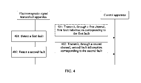
in the fault register
includes the first fault information. The information in the fault register
may have 32 bits or 64
bits, and the following uses an example in which the information in the fault
register has 32 bits.
If no fault occurs, the information in the fault register is
0000000000000000000000000000000000.
If one fault occurs, 1 bit in the 32 bits changes from 0 to 1, for example,
00000100000000000000000000000000. If two faults occur, 2 bits in the 32 bits
change from 0 to
1, for example, 00100100000000000000000000000000. In other words, 1 indicates
that a fault
occurs, and 0 indicates that no fault occurs.
[00138] Further, the electromagnetic signal transceiver apparatus may send the
information in
the fault register to the control apparatus, where the information in the
fault register includes the
first fault information. Correspondingly, the control apparatus may receive
the information in the
fault register from the electromagnetic signal transceiver apparatus. Further,
optionally, the first
processor in the control apparatus may identify the first fault information in
the information in the
fault register. For example, if the information in the fault register that is
received by the first
processor is 000001000000000000000000000 00000, the first processor may
identify that the sixth
bit is the first fault information, that is, the first fault information is in
the sixth bit. For another
example, if the information in the fault register that is received by the
first processor is
00100100000000000000000000000000, the first processor performs identification
in sequence,
and identifies that the third bit is the first fault information, that is, the
first fault information is in
the third bit.
[00139] Step 402: The electromagnetic signal transceiver apparatus detects a
second fault, and
may transmit, to the control apparatus through a second channel, second fault
information
corresponding to the second fault. Correspondingly, the control apparatus
obtains the second fault
information through the second channel.
[00140] In a further optional design of step 402, the second fault information
is transmitted to
the second processor in the control apparatus through the second channel,
and/or the second
processor in the control apparatus obtains the second fault information
transmitted through the
second channel.
[00141] Herein, the second channel may be a data channel, for example, an LVDS
channel or a
mobile industry processor interface (mobile industry processor interface,
MIPI).
[00142] In an optional design, the first channel is an SPI, and the second
channel is an LVDS
channel. In this way, when being applied to a millimeter-wave radar, the
solution can be compatible
with the SPI and the LVDS channel in the existing millimeter-wave radar.
CA 03197021 2023- 4- 28 19
[00143] In a possible implementation, the second fault information may be
stored in a first
memory in the control apparatus. In other words, the electromagnetic signal
transceiver apparatus
transmits the second fault information to the first memory in the control
apparatus through the
second channel.
[00144] The following shows two example possible implementations of obtaining
the second
fault information by the second processor.
[00145] Implementation 1: The second processor detects a second Fl hardwire
flag, where the
second Fl hardwire flag is used to indicate that the second fault occurs on
the electromagnetic
signal transceiver apparatus. The second processor obtains the second fault
information from the
first memory.
[00146] Implementation 2: The second processor periodically queries the first
memory, and
obtains the second fault information from the first memory. For example, the
second processor
may periodically query the first memory, and identify the second fault
information. For a possible
identification manner, refer to related description of step 509 in FIG. 5. In
this case, no Fl hardwire
flag needs to be triggered.
[00147] Based on Implementation 1 or Implementation 2, when detecting the
second fault, the
electromagnetic signal transceiver apparatus may send the information in the
fault register to the
control apparatus through the LVDS channel. Correspondingly, the control
apparatus may receive
the information in the fault register from the electromagnetic signal
transceiver apparatus through
the LVDS channel. Further, the second processor in the control apparatus may
obtain (or referred
to as "identify") the information in the fault register, and identify the
second fault information from
the information in the fault register.
[00148] For example, the information in the fault register that is obtained by
the second
processor from the first memory in the control apparatus is
00100100000000000000000000000000, and the second processor reads, from a cache
of the first
processor, that the sixth bit (that is, the first fault information) in the
information in the fault register
has been processed by the first processor. When identifying the information
00100100000000000000000000000000 in the fault register, the second processor
shields the sixth
bit, that is, skip identifying the first fault information in the sixth bit.
The second processor
identifies the third bit and determines the third bit as the second fault
information.
[00149] For another example, the information in the fault register that is
read by the second
processor from the first memory in the control apparatus is
00000100010000000000000000000000, and the second processor reads, from the
cache of the
first processor, that a fault (that is, the first fault information) in the
sixth bit of the information in
the fault register has been processed by the first processor. When identifying
the information
CA 03197021 2023- 4- 28 20
00000100010000000000000000000000 in the fault register, the second processor
shields the sixth
bit, that is, skip identifying the fault information in the sixth bit. The
second processor continues
to identify bits after the sixth bit until identifying the tenth bit, and
determines the tenth bit as the
second fault information.
[00150] It can be learned from step 401 and step 402 that, the second
processor may process
the second fault simultaneously when the first processor processes the first
fault, so that each fault
in a dual-point fault can be processed in time as much as possible. In
addition, the first fault
information and the second fault information are sent through two channels,
which helps avoid a
case in which a communication channel fails because a single channel is used.
[00151] After obtaining the second fault information, the control apparatus
may process the
second fault corresponding to the second fault information. The following
shows three example
possible manners of triggering the second processor to process the second
fault.
[00152] Manner 1: The second processor receives a first instruction from the
first processor.
[00153] In a possible implementation, when detecting the first Fl hardwire
flag, the first
processor may further send the first instruction to the second processor,
where the first instruction
is used to instruct the second processor to process the second fault.
Correspondingly, the second
processor may receive the first instruction from the first processor, and
process the second fault in
response to the first instruction.
[00154] It should be understood that if the first processor in the control
apparatus detects the Fl
hardwire flag, it indicates that a fault (referred to as the first fault) has
occurred in the
electromagnetic signal transceiver apparatus. In this case, the first
processor needs to process the
first fault. To avoid that a new fault generated by the electromagnetic signal
transceiver apparatus
in a task periodicity in which the first processor processes the first fault
cannot be processed in
time, the second processor needs to start a fault processing interrupt task to
process, in time, the
new fault (referred to as the second fault) generated by the electromagnetic
signal transceiver
apparatus. Based on this, the first instruction may be used to instruct the
second processor to
process the second fault. Specifically, the first instruction may directly
instruct the second
processor to process the second fault; or the first instruction indirectly
instructs the second
processor to process the second fault. For example, the first instruction
indicates that the first
processor is occupied to process the first fault, or instructs the second
processor to start a fault
processing task, so that when the second fault is generated, the second
processor can process the
second fault.
[00155] In a possible implementation, the first instruction may trigger a
software flag bit in the
second processor, and the second processor reads, in a storage area
corresponding to the software
flag bit, a fault processing task corresponding to the software flag bit.
CA 03197021 2023- 4- 28 21
[00156] Manner 2: The second processor detects a second Fl hardwire flag.
[00157] Based on Manner 2, the second processor may process the second fault
in response to
detection of the second Fl hardwire flag. It should be understood that if the
second processor
detects the second Fl hardwire flag, it indicates that the second fault has
occurred, and the second
processor may be triggered herein to process the second fault.
[00158] Manner 3: The second processor determines that processing of the first
fault is
uncompleted.
[00159] Based on Manner 3, the second processor may process the second fault
in response to
uncompleted processing of the first fault. It should be understood that the
first processor does not
complete processing of the first fault. In this case, the first processor
needs to process the first fault.
To avoid that a new fault generated by the electromagnetic signal transceiver
apparatus in a task
periodicity in which the first processor processes the first fault cannot be
processed in time, the
second processor needs to start a fault processing task.
[00160] It should be noted that any combination of the foregoing three manners
may
alternatively trigger the second processor to process the second fault. For
example, when the
second processor determines that processing of the first fault is uncompleted
and detects the second
Fl hardwire flag (that is, a combination of Manner 2 and Manner 3), the second
processor processes
the second fault in response to uncompleted processing of the first fault and
detection of the second
Fl hardwire flag. It should be understood that if the second processor detects
the second Fl
hardwire flag, it indicates that the second fault has occurred. In addition,
the first processor does
not complete processing of the first fault. To enable the first fault and the
second fault to be
processed in time as much as possible, the second processor needs to process
the second fault.
[00161] The following description is provided by using an example in which the
first Fl
hardwire flag is an Fl hardwire flag, the second Fl hardwire flag is a second
fault indication (fault
second indication, FSI) hardwire flag, the first memory is a RAM in an MCU,
the electromagnetic
signal transceiver apparatus is an MMIC, the control apparatus is the MCU, the
first processor is
a first CPU, the second processor is a second CPU, the first channel is an
SPI, and the second
channel is an LVDS channel. In other words, in subsequent description of this
application, each
RAM may be replaced with the first memory, each MMIC may be replaced with the
electromagnetic signal transceiver apparatus, each MCU may be replaced with
the control
apparatus, each first CPU may be replaced with the first processor, each
second CPU may be
replaced with the second processor, each Fl hardwire flag may be replaced with
the first Fl
hardwire flag, each FSI hardwire flag may be replaced with the second Fl
hardwire flag, each SPI
may be replaced with the first channel, and each LVDS channel may be replaced
with the second
channel. The following is merely an example description for ease of
description.
CA 03197021 2023- 4- 28 22
[00162] FIG. 5 shows another information transmission method according to this
application.
The information transmission method may be applied to the millimeter-wave
radar system shown
in FIG. 3. The method may include the following steps.
[00163] Step 501: An MMIC detects a first fault, and sends an Fl hardwire flag
to a first CPU.
[00164] With reference to FIG. 3, the control unit 3021 in the MMIC 302 may
detect the first
fault, and send an Fl hardwire flag to the CPU 3011 by using an Fl hardwire
pin connected to a
pin of the MCU 301.
[00165] It should be understood that the MMIC may start to detect a fault
based on an
instruction a sent by the first CPU.
[00166] Step 502: The first CPU in an MCU detects the Fl hardwire flag, and
sends a first
instruction to a second CPU in the MCU. Correspondingly, the second CPU
receives the first
instruction from the first CPU.
[00167] Herein, each pin of the MCU has a corresponding flag, and the flag
corresponding to
the pin may be stored in a register of the MCU. A pin of the MCU is connected
to an Fl hardwire
pin, and the register stores a flag bit (referred to as an Fl hardwire flag
bit) of the pin connected to
the Fl hardwire pin. The first CPU may periodically detect the Fl hardwire
flag bit in the register
of the MCU, to determine whether the MMIC is faulty. For example, if the CPU
detects that the
Fl hardwire flag is 1, it indicates that a fault occurs in the MMIC. For
description of the first
instruction, refer to the foregoing related content. Details are not described
herein again.
[00168] Step 503: The first CPU in the MCU sends a first request message to
the MMIC.
Correspondingly, the MMIC receives the first request message from the first
CPU in the MCU.
[00169] The first request message is used to request first fault information,
or the first request
message is used to request the MMIC to query a fault register, to obtain the
first fault information.
[00170] Step 504: The MMIC queries the fault register based on the first
request message.
[00171] Herein, the MMIC may query information in the fault register based on
the first request
message. It should be noted that the MMIC is a passive component, and can only
determine that a
fault occurs, but cannot identify a specific faulty bit in the fault register.
[00172] Step 505: The MMIC may send the information in the fault register to
the first CPU.
Correspondingly, the first CPU may receive the information in the fault
register from the MMIC
and buffer the information.
[00173] Herein, the information in the fault register includes the first fault
information.
[00174] In a possible implementation, the MMIC may send the information in the
fault register
to the first CPU through an SPI. Correspondingly, the first CPU may receive
the information in
the fault register from the MMIC through the SPI and buffer the information.
[00175] When a data amount of the found information in the fault register is
relatively large,
CA 03197021 2023- 4- 28 23
the MMIC may need to send the information in the fault register to the first
CPU a plurality of
times. For the information in the fault register, refer to the foregoing
related description. Details
are not described herein again.
[00176] Step 506: The first CPU in the MCU determines (or referred to as
"identifies") the first
fault information in the information in the fault register.
[00177] Herein, for a process in which the first CPU identifies the first
fault information in the
information in the fault register, refer to the foregoing related description.
Details are not described
herein again. It should be noted that after identifying the first fault
information, the first CPU does
not continue to identify a subsequent bit, and may perform the following step
507.
[00178] Step 507: The first CPU in the MCU processes the first fault.
[00179] In a possible implementation, fault processing software deployed in
the first CPU
includes a fault processing policy, and the fault processing policy includes
but is not limited to a
correspondence between a fault level and a processing method. For example, if
the fault level is a
minor fault, the MMIC is reset; if the fault cannot be recovered for three
times, the MMIC is
powered off; or if the fault level is a critical fault, the MMIC is directly
powered off For example,
the first CPU may first determine a level of the first fault, and perform
corresponding processing
on the first fault based on the level of the first fault.
[00180] Step 508: The MMIC detects a second fault, and may send the
information in the fault
register to the MCU through an LVDS channel. Correspondingly, the MCU may
receive the
information in the fault register from the MMIC through the LVDS channel.
[00181] Herein, the information in the fault register may be stored in a RAM
of the MCU, and
the information in the fault register includes second fault information.
[00182] With reference to FIG. 3, when detecting the second fault, the MMIC
302 may send the
information in the fault register to the RAM 3013 in the MCU 301 through the
LVDS channel.
Correspondingly, the RAM 3013 in the MCU 301 stores the information in the
fault register. In
other words, when the MMIC 302 detects the second fault, the LVDS channel is
no longer used to
transmit normal service data to the RAM 3013 in the MCU 301, and instead, the
LVDS channel is
multiplexed to transmit the information in the fault register to the RAM 3013
in the MCU 301.
[00183] Herein, when detecting the second fault, the MMIC can only determine
that two faults
occur, and cannot determine two specific bits that are faulty in the fault
register. For example, the
information in the fault register is 00100100000000000000000000000000, and the
MMIC sends
the information 00100100000000000000000000000000 in the fault register to the
RAM in the
MCU through the LVDS channel. Correspondingly, the RAM in the MCU may store
00100100000000000000000000000000. For another example, the information in the
fault register
is 00000100010000000000000000000000, and the MMIC sends the information
CA 03197021 2023- 4- 28 24
00000100010000000000000000000000 in the fault register to the RAM in the MCU
through the
LVDS channel. Correspondingly, the RAM in the MCU may store
00000100010000000000000000000000.
[00184] In a possible implementation, after detecting the Pt fault, the MMIC
keeps continuing
to detect a fault, and the 2nd fault may be detected at any time in a task
periodicity of the 1' fault
after the 1' fault is detected.
[00185] It should be noted that step 508 may be any step after step 501 and
before step 509.
[00186] Step 509: The second CPU in the MCU obtains (or referred to as
"identifies") the
second fault information in the information in the fault register.
[00187] The following shows two example possible implementations in which the
second CPU
in the MCU obtains the second fault information in the information in the
fault register.
[00188] Implementation 1: The second CPU detects an FSI hardwire flag, and
obtains the
second fault information from a RAM in the MCU.
[00189] With reference to FIG. 3, the CPU 3011 is connected to the control
unit 3021 by using
an Fl hardwire pin, and the CPU 3012 is connected to the control unit 3021 by
using an FSI
hardwire pin. In other words, an FSI hardwire flag used for fault indication
is set between the
MMIC 302 and the MCU 301. The control unit 3021 in the MMIC 302 detects the
second fault,
and sends an FSI hardwire flag to the CPU 3012 by using an FSI hardwire pin
connected to a pin
of the MCU 301. For example, two hardwire flag bits (that is, an Fl hardwire
flag bit and an FSI
hardwire flag bit) are preconfigured in firmware deployed in the MMIC, and a
function of an FSI
hardwire pin and a function of an Fl hardwire pin are controlled by using
software. That is, when
the firmware deployed by the MMIC detects a fault for the first time, the Fl
hardwire flag bit is
triggered; and when the firmware detects a fault for the second time, the FSI
hardwire flag bit is
triggered.
[00190] Based on Implementation 1, after detecting the 2nd fault, the MMIC
triggers the FSI
hardwire flag bit, for example, sets the FSI hardwire flag bit to a high level
(for example, 1).
[00191] Herein, the second CPU executes tasks in serial, and detecting the FSI
hardwire flag is
one of the tasks. Generally, a task of processing an FSI hardwire flag
interrupt has a highest priority.
For example, the second CPU needs to execute a task 1 (that is, detecting the
FSI hardwire flag),
a task 2, and a task 3, and the second CPU may run the three tasks in sequence
based on priorities.
For example, a priority of the task 1 is higher than that of the task 2, and a
priority of the task 2 is
higher than that of the task 3. The first CPU runs the task 1, the task 2, and
the task 3 in sequence.
When detecting that the task 1 occurs, the second CPU may enter the task 1,
that is, execute a
procedure of the task 1.
[00192] When detecting the FSI hardwire flag, the second CPU in the MCU reads
the
CA 03197021 2023- 4- 28 25
information in the fault register from the RAM in the MCU, and reads, from a
cache (cache) of the
first CPU, the first fault information in the information in the fault
register. In addition, when
determining that the first fault has been processed by the first CPU, the
second CPU shields the
first fault information, and identifies the second fault information from the
information in the fault
register.
[00193] For a possible implementation in which the second CPU identifies the
second fault
information from the information in the fault register, refer to the foregoing
related descriptions.
Details are not described herein again.
[00194] Implementation 2: The second CPU periodically queries the RAM in the
MCU, and
obtains the second fault information from the RAM in the MCU.
[00195] Based on Implementation 2, the second CPU periodically reads the
information in the
fault register from the RAM in the MCU, and reads, from a cache of the first
CPU, the first fault
information in the information in the fault register. In addition, when
determining that the first
fault has been processed by the first CPU, the second CPU shields the first
fault information, and
identifies the second fault information from the information in the fault
register.
[00196] For an example in which the second CPU identifies the second fault
information from
the read information in the fault register, refer to related descriptions in
Implementation 1. Details
are not described herein again.
[00197] In a possible implementation, the second CPU may periodically query
the RAM in the
MCU, for example, query the RAM every 1 ms.
[00198] Step 510: The second CPU in the MCU processes the second fault.
[00199] For step 510, refer to step 507. Details are not described herein
again.
[00200] It can be learned from step 501 to step 510 that the first CPU
processes the first fault,
and the second CPU processes the second fault, so that the first fault and the
second fault can be
processed in time. In addition, a manner of sending the information in the
fault register by
multiplexing the LVDS channel is a heterogeneous redundancy manner, which
helps avoid a case
in which all communication channels fail because a single SPI communication
manner is used.
[00201] After step 502, that is, after receiving the first instruction, the
second CPU may start a
fault processing task in response to the first instruction. FIG. 6 is a
schematic flowchart of another
information transmission method according to this application. In the method,
for example, that
an Fl hardwire flag bit is 1 indicates an Fl hardwire flag interrupt (that is,
an Fl hardwire flag is
triggered), and that an FSI hardwire flag bit is 1 indicates an FSI hardwire
flag interrupt (that is,
an FSI hardwire flag is triggered).
[00202] Step 601: A second CPU clears data in a RAM in an MCU.
[00203] Herein, the second CPU may send a data clear instruction to the RAM in
the MCU, and
CA 03197021 2023- 4- 28 26
the RAM in the MCU clears stored data based on the data clear instruction. In
this way, original
data in the RAM in the MCU can be prevented from interfering with a fault
interrupt processing
task.
[00204] It should be noted that after the second CPU receives a first
instruction, the RAM in
the MCU has not received information about a fault register from an MMIC. In
other words, before
the information in the fault register is received, the data in the RAM in the
MCU is cleared first,
so that after receiving the information in the fault register, the RAM in the
MCU stores only the
information in the fault register.
[00205] Step 602: The second CPU determines whether the Fl hardwire flag is 1;
and performs
step 603 if the Fl hardwire flag is 1; or performs step 604 if the Fl hardwire
flag is not 1.
[00206] Herein, if the Fl hardwire flag is 1, it indicates that a first CPU
does not complete
processing of a first fault. If a second fault occurs in the MMIC, the first
CPU cannot process the
second fault in time. Therefore, the second CPU needs to process the second
fault. If it is
determined that the Fl hardwire flag is 0, it indicates that the first CPU has
processed the first fault.
In this case, if the second fault occurs in the MMIC, the first CPU may
directly process the second
fault, and the second CPU does not need to process the second fault. Herein,
the second CPU may
perform subsequent step 604 and step 605.
[00207] Step 603: The second CPU determines whether the FSI hardwire flag is
1; and performs
the following step 606 if the FSI hardwire flag is 1; or returns to perform
step 602 if the FSI
hardwire flag is not 1.
[00208] Herein, if the FSI hardwire flag is 1, it indicates that the second
CPU does not complete
processing of the second fault, and therefore the second CPU needs to process
the second fault,
that is, perform step 606. If the FSI hardwire flag is 0, it indicates that
the second fault has been
processed, and the second CPU returns to step 602 to wait for a new fault
processing task again.
[00209] Step 604: The second CPU clears the RAM in the MCU. Step 605 is
performed after
step 604.
[00210] Step 605: The second CPU exits a fault processing task.
[00211] Step 606: The second CPU processes the second fault.
[00212] If the second CPU obtains the second fault information based on
Implementation 1,
after completing processing of the second fault, the second CPU further needs
to clear the FSI
hardwire flag corresponding to the second fault and/or the second fault
information in the
information in the fault register. Refer to the description in FIG. 7.
[00213] Step 701. The second CPU may send a second instruction to the MMIC.
Correspondingly, the MMIC receives the second instruction from the second CPU
by using the
SPI.
CA 03197021 2023- 4- 28 27
[00214] In a possible implementation, the second CPU may send the second
instruction to the
MMIC through an SPI.
[00215] Herein, the second instruction is used to instruct the MMIC to clear
the FSI hardwire
flag and/or the second fault information. With reference to FIG. 3, the CPU
1302 may send the
second instruction to the control unit 3021 in the MMIC 302. The second
instruction is used to
instruct the control unit 3021 to clear the second fault information and/or
clear the FSI hardwire
flag. For example, the control unit 3021 may restore the second fault
information 1 to 0, and set
the FSI hardwire flag bit to a low level (for example, 0).
[00216] Step 702: The MMIC may clear, based on the second instruction, the
second fault
information included in the information in the fault register and/or the FSI
hardwire flag.
[00217] With reference to step 509 in FIG. 5, for example, the information in
the fault register
is 001001000000000000000000000 00000, and the second fault information is the
third bit in the
information in the fault register. The MMIC may restore 1 in the third bit to
0 based on the second
instruction. For another example, the information in the fault register is
00000100010000000000000000000000, and the second fault information is the
tenth bit in the
information in the fault register. The MMIC may restore 1 in the tenth bit to
0 based on the second
instruction.
[00218] Herein, if "the Fl hardwire flag is 1" indicates interruption, the
MMIC may restore the
Fl hardwire flag to 0 based on the second instruction.
[00219] Step 703: The MMIC may send a third response to the second CPU.
[00220] In a possible implementation, the MMIC may send the third response to
the second
CPU through an SPI.
[00221] Herein, the third response includes an execution process of the second
instruction. For
example, the execution process of the second instruction may be identified by
0 and 1, where 0
indicates that execution of the second instruction is uncompleted, and 1
indicates that execution of
the second instruction is completed. It should be noted that execution of the
second instruction
may alternatively be represented by another identifier, provided that the
identifier can distinguish
whether the second instruction is completed or uncompleted. This is not
limited in this application.
[00222] It should be understood that the second CPU needs to determine a
process of executing
the second instruction by the MMIC. Therefore, the MMIC periodically feeds
back an execution
process of the second instruction to the second CPU. For example, the MMIC may
feed back the
execution process of the second instruction to the second CPU once every 10
us.
[00223] Step 704: The second CPU determines, based on the received third
response, whether
the MMIC completes execution of the second instruction; and performs step 705
if execution of
the second instruction is completed; or if execution of the second instruction
is uncompleted,
CA 03197021 2023- 4- 28 28
continues to detect the execution process of the second instruction, that is,
cyclically performs step
704.
[00224] For example, the second CPU sends the second instruction at a moment
tl , and views
the third response at a moment t2. The moment tl and the moment t2 may be
preset. That is, the
CPU usually sends an instruction and receives a response based on fixed
duration.
[00225] Step 705: The second CPU exits a fault processing task.
[00226] It can be learned from step 701 to step 705 that, after completing
processing of the
second fault, the second CPU clears, in time, the FSI hardwire flag and/or the
second fault
information corresponding to the second fault, so that a newly generated fault
can be processed in
time in a next task periodicity.
[00227] It should be noted that in the foregoing embodiment, execution
processes of steps in
the first CPU are serial, execution processes of steps in the second CPU are
serial, and execution
processes of the first CPU and the second CPU may be serial or parallel. It
should be noted that
the execution processes of the foregoing steps are described for clearly
explaining a solution.
Based on a requirement in an actual scenario, one or more steps in the
foregoing steps may not
need to be performed, or a plurality of steps may be combined for execution.
This depends on
specific execution in an actual scenario.
[00228] It may be understood that, to implement the functions in the foregoing
embodiments,
the control apparatus includes corresponding hardware structures and/or
software modules for
performing the functions. A person skilled in the art should be easily aware
that, modules and
method steps in the examples described with reference to embodiments disclosed
in this
application can be implemented in this application by hardware or a
combination of hardware and
computer software. Whether a function is performed by hardware or hardware
driven by computer
software depends on particular application scenarios and design constraint
conditions of the
technical solutions.
[00229] Based on the foregoing content and a same concept, FIG. 8 is a
schematic diagram of
a possible structure of a control apparatus according to this application. The
control apparatus can
be configured to implement functions of the control apparatus in the foregoing
method
embodiments, and therefore beneficial effects of the foregoing method
embodiments can also be
implemented. In this application, the control apparatus may be the MCU 301
shown in FIG. 3.
[00230] As shown in FIG. 8, the control apparatus 800 includes a first
processor 801 and a
second processor 802. Further, the control apparatus 800 may include a first
interface circuit 803
and a second interface circuit 804. Optionally, the control apparatus 800 may
further include a first
memory 805 and/or a second memory 806. The first memory 805 may be configured
to store
instructions executed by the first processor 801 and the second processor 802.
The second memory
CA 03197021 2023- 4- 28 29
806 may be configured to store second fault information received by the
control apparatus 800.
The control apparatus 800 may be configured to implement functions of the
control apparatus or
the MCU in the method embodiment shown in FIG. 4, FIG. 5, FIG. 6, or the
figure. It should be
noted that the first interface circuit 803 may also be referred to as a first
input/output interface 803,
and the second interface circuit 804 may also be referred to as a second
input/output interface 804.
The interface circuit is introduced herein to better describe a hardware
structure of a product. A
person skilled in the art may understand that the interface circuit may be a
hardware circuit or a
logic circuit that implements a corresponding channel. "By using an interface
circuit corresponding
to a channel" appears in the following may also be directly understood or
replaced with "through
a channel".
[00231] When the control apparatus 800 is configured to implement functions of
the control
apparatus in the method embodiment shown in FIG. 4, the first processor 801 is
configured to
obtain first fault information of an electromagnetic signal transceiver
apparatus by using the first
interface circuit 803 corresponding to a first channel, where the first fault
information corresponds
to a first fault; and the second processor 802 is configured to obtain second
fault information of
the electromagnetic signal transceiver apparatus, where the second fault
information corresponds
to a second fault. The second fault information is from the electromagnetic
signal transceiver
apparatus and is transmitted by using the second interface circuit 804
corresponding to a second
channel.
[00232] More detailed descriptions of the first processor 801 and the second
processor 802 may
be directly obtained by referring to related descriptions in the method
embodiment shown in FIG.
4. Details are not described one by one herein again.
[00233] Based on the foregoing content and a same concept, FIG. 9 is a
schematic diagram of
a possible structure of an electromagnetic signal transceiver apparatus
according to this application.
The electromagnetic signal transceiver apparatuses can be configured to
implement functions of
the electromagnetic signal transceiver apparatus in the foregoing method
embodiments, and
therefore beneficial effects of the foregoing method embodiments can also be
implemented. In this
application, the electromagnetic signal transceiver apparatus may be the MMIC
302 shown in FIG.
3.
[00234] As shown in FIG. 9, the electromagnetic signal transceiver apparatus
900 includes a
controller 901, and may further include a fourth interface circuit 902 and a
fifth interface circuit
903. Optionally, the control apparatus 900 may further include a memory 904,
and the memory
904 may be configured to store fault information. It should be noted that
instructions executed by
the controller 901 are usually firmware (firmware) programs, that is, the
instructions executed by
the controller 901 are usually fixed in the electromagnetic signal transceiver
apparatus 900. The
CA 03197021 2023- 4- 28 30
electromagnetic signal transceiver apparatus 900 is configured to implement
functions of the
electromagnetic signal transceiver module or the MMIC in the method embodiment
shown in FIG.
4, FIG. 5, FIG. 6, or the figure. It should be noted that the fourth interface
circuit 902 may also be
referred to as a fourth input/output interface 902, and the fifth interface
circuit 903 may also be
referred to as a fifth input/output interface 903. For explanation of the
interface circuit herein, refer
to the foregoing description. Further, optionally, the memory 904 may include
a register.
[00235] When the electromagnetic signal transceiver apparatus 900 is
configured to implement
functions of the electromagnetic signal transceiver apparatus in the method
embodiment shown in
FIG. 4, the controller 901 is configured to detect a first fault, and transmit
first fault information
to a control apparatus by using the fourth interface circuit 902 corresponding
to a first channel,
where the first fault information corresponds to the first fault; and the
controller 901 is further
configured to detect a second fault, and transmit second fault information to
the control apparatus
by using the fifth interface circuit 903 corresponding to a second channel,
where the second fault
information corresponds to the second fault.
[00236] More detailed descriptions of the controller 901 may be directly
obtained by referring
to related descriptions in the method embodiment shown in FIG. 4. Details are
not described one
by one herein again.
[00237] Based on the foregoing content and a same concept, as shown in FIG.
10, this
application further provides a signal processing device 1000. The signal
processing device 1000
may include at least one of the control apparatus 800 or the electromagnetic
signal transceiver
apparatus 900. For the control apparatus 800, refer to related descriptions in
FIG. 8. For the
electromagnetic signal transceiver apparatus 900, refer to related
descriptions in FIG. 9.
[00238] When the signal processing device 1000 is configured to implement the
method shown
in FIG. 4, the control apparatus 800 is configured to perform functions of the
control apparatus,
and the electromagnetic signal transceiver apparatus 900 is configured to
perform functions of the
electromagnetic signal transceiver apparatus.
[00239] It may be understood that the processor in embodiments of this
application may be a
central processing unit (central processing unit, CPU), or may be another
general-purpose
processor, a digital signal processor (digital signal processor, DSP), an
application-specific
integrated circuit (application-specific integrated circuit, ASIC), a field
programmable gate array
(field programmable gate array, FPGA) or another programmable logic device, a
transistor logic
device, a hardware component, or any combination thereof The general-purpose
processor may
be a microprocessor or may be any conventional processor. The controller may
be, for example, a
control unit (control unit) in a millimeter-wave radar system, an application-
specific integrated
circuit (application-specific integrated circuit, ASIC), a field programmable
gate array (field
CA 03197021 2023- 4- 28 31
programmable gate array, FPGA) or another programmable logic device, a
transistor logic device,
a hardware component, or any combination thereof
[00240] The method steps in embodiments of this application may be implemented
by using
hardware, or may be implemented by executing software instructions by the
processor. The
software instructions may include a corresponding software module. The
software module may be
stored in a random access memory (random access memory, RAM), a flash memory,
a read-only
memory (read-only memory, ROM), a programmable read-only memory (programmable
ROM,
PROM), an erasable programmable read-only memory (erasable PROM, EPROM), an
electrically
erasable programmable read-only memory (electrically EPROM, EEPROM), a
register, a hard
disk, a removable hard disk, a CD-ROM, or any other form of storage medium
well-known in the
art. An example storage medium is coupled to the processor, so that the
processor can read
information from the storage medium and write information into the storage
medium. Certainly,
the storage medium may be a component of the processor. The processor and the
storage medium
may be located in an ASIC. In addition, the ASIC may be located in a control
apparatus or an
electromagnetic signal transceiver apparatus. Certainly, the processor and the
storage medium may
exist in a network device or a terminal device as a discrete component.
[00241] All or some of the foregoing embodiments may be implemented by using
software,
hardware, firmware, or any combination thereof When software is used to
implement the
embodiments, all or some of the embodiments may be implemented in a form of a
computer
program product. The computer program product includes one or more computer
programs or
instructions. When the computer programs or instructions are loaded and
executed on a computer,
all or some of the procedures or functions in embodiments of this application
are performed. The
computer may be a general-purpose computer, a dedicated computer, a computer
network, a
network device, user equipment, or another programmable apparatus. The
computer programs or
instructions may be stored in a computer-readable storage medium or may be
transmitted from one
computer-readable storage medium to another computer-readable storage medium.
For example,
the computer programs or instructions may be transmitted from one website,
computer, server, or
data center to another website, computer, server, or data center in a wired or
wireless manner. The
computer-readable storage medium may be any available medium accessible by a
computer or a
data storage device, such as a server or a data center, that integrates one or
more available media.
The available medium may be a magnetic medium, for example, a floppy disk, a
hard disk, or a
magnetic tape; may be an optical medium, for example, a digital video disc
(digital video disc,
DVD); or may be a semiconductor medium, for example, a solid state drive
(solid state drive, SSD).
[00242] In embodiments of this application, unless otherwise stated or there
is a logic conflict,
terms and/or descriptions between different embodiments are consistent and may
be mutually
CA 03197021 2023- 4- 28 32
referenced, and technical features in different embodiments may be combined
based on an internal
logical relationship of the embodiments, to form a new embodiment.
[00243] In this application, the word "example" is used to represent giving an
example, an
illustration, or a description. Any embodiment or design solution described as
an "example" in this
application should not be explained as being more preferred or having more
advantages than
another embodiment or design solution. Alternatively, this may be understood
as that use of the
word "example" is intended to present a concept in a specific manner, and does
not constitute a
limitation on this application.
[00244] It may be understood that various numerical numbers in embodiments of
this
application are merely used for differentiation for ease of description, and
are not used to limit the
scope of embodiments of this application. Sequence numbers of the foregoing
processes do not
mean execution sequences. The execution sequences of the processes should be
determined based
on functions and internal logic of the processes. The terms "first", "second",
and another similar
expression are used to distinguish between similar objects but are
unnecessarily used to describe
a specific order or sequence. In addition, the terms "include", "have", and
any variant thereof are
intended to cover non-exclusive inclusion, for example, include a series of
steps or modules.
Methods, systems, products, or devices are unnecessarily limited to those
steps or modules that
are clearly listed, but may include other steps or modules that are not
clearly listed or that are
inherent to these processes, methods, products, or devices.
[00245] Apparently, a person skilled in the art can make various modifications
and variations
to this application without departing from the protection scope of this
application. This application
is intended to cover these modifications and variations of this application
provided that they fall
within the scope of the claims of this application and an equivalent
technology thereof
CA 03197021 2023- 4- 28 33