Note: Descriptions are shown in the official language in which they were submitted.
PHASE-LOCKED LOOP CIRCUIT AND SIGNAL PROCESSING
DEVICE
CROSS-REFERENCE TO RELATED APPLICATIONS
This application claims priority to Chinese Patent Application No.
202110848675.1,
entitled "PHASE-LOCKED LOOP CIRCUIT AND SIGNAL PROCESSING DEVICE", and
filed on July 27, 2021, the disclosure of which is incorporated herein by
reference in its entirety.
TECHNICAL FIELD
The present disclosure relates to the technical field of electronic circuits,
and in particular,
to a phase-locked loop circuit and a signal processing device.
BACKGROUND
A phase-locked loop circuit is a feedback control circuit which can control
the frequency
and the phase of the oscillation signal inside the loop with the reference
signal input outside,
to achieve the automatic tracking of the output frequency to the input
frequency. A plurality of
signal processing devices such as a mobile communication base station and a
frequency
hopping communication system have the strict requirement for the locking time
of the phase-
locked loop circuit. Since the locking time of the phase-locked loop circuit
is directly related
to the loop bandwidth thereof, the locking time can be reduced by increasing
the loop
bandwidth, thereby speeding up the frequency locking. However, the change in
the loop
bandwidth may lead to the change in other parameter in the phase-locked loop
circuit, which
leads to the deterioration of the performance.
SUMMARY
The present disclosure is intended to provide a phase-locked loop circuit and
a signal
processing device.
According to a first aspect of the present disclosure, the phase-locked loop
circuit is
provided, including: a charge pump configured with a charge pump current; and
a loop filter
connected to the charge pump and configured with a first resistance value, a
first capacitance
value, and a second capacitance value, wherein a zero frequency of the phase-
locked loop
circuit is configured to be determined by the first resistance value and the
first capacitance
1
CA 03202290 2023- 6- 14
value, and a pole frequency of the phase-locked loop circuit is configured to
be determined by
the first resistance value and the second capacitance value; wherein at least
two of the charge
pump current, the first resistance value, the first capacitance value, and the
second capacitance
value are adjustable, to change a loop bandwidth of the phase-locked loop
circuit, to maintain
a first ratio between the zero frequency and the loop bandwidth unchanged, and
to maintain a
second ratio between the pole frequency and the loop bandwidth unchanged.
According to a second aspect of the present disclosure, the signal processing
device is
provided, including the phase-locked loop circuit as described above.
Through detailed description of exemplary embodiments of the present
disclosure with
reference to the following drawings, other features and advantages of the
present disclosure
will become clear.
BRIEF DESCRIPTION OF THE DRAWINGS
The drawings that constitute a part of the description describe embodiments of
the present
disclosure, and are used to explain the principle of the present disclosure
together with the
description.
The present disclosure can be understood more clearly according to the
following detailed
description with reference to the accompanying drawings.
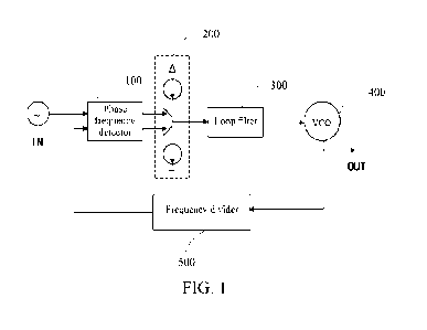
FIG. 1 shows a structural block diagram of a phase-locked loop circuit.
FIG. 2 shows a schematic circuit diagram of a charge pump and a loop filter in
a phase-
locked loop circuit.
FIG. 3 shows a schematic circuit diagram of a charge pump in a phase-locked
loop circuit
according to an exemplary embodiment of the present disclosure.
FIG. 4 shows a schematic diagram of a bias potential generation circuit
according to an
exemplary embodiment of the present disclosure.
FIG. 5 shows a schematic circuit diagram of a charge pump in a phase-locked
loop circuit
according to another exemplary embodiment of the present disclosure.
FIG. 6 shows a schematic circuit diagram of a loop filter in a phase-locked
loop circuit
according to an exemplary embodiment of the present disclosure.
FIG. 7 shows a schematic circuit diagram of a loop filter in a phase-locked
loop circuit
according to another exemplary embodiment of the present disclosure.
FIG. 8 shows a schematic circuit diagram of a loop filter in a phase-locked
loop circuit
according to still another exemplary embodiment of the present disclosure.
2
CA 03202290 2023- 6- 14
It is to be noted that in the implementations illustrated below, sometimes the
same
reference numeral is used in different drawings to represent the same part or
a part with the
same function, and repeated illustration thereof is omitted. In the
description, similar numbers
and letters are used to represent similar items. Therefore, once an item is
defined in a drawing,
the item in subsequent drawings is not further discussed.
For ease of understanding, the locations, sizes, ranges, and the like of
various structures
shown in the drawings sometimes do not represent the actual locations, sizes,
ranges, and the
like. Therefore, the disclosed invention is not limited to the locations, the
sizes, the ranges, and
the like disclosed in the drawings. Moreover, the drawings are not necessarily
drawn to scale,
and some features may be exaggerated to show the details of specific
components.
DETAILED DESCRIPTION
Various exemplary embodiments of the present disclosure will be described in
detail with
reference to the drawings now. It is to be noted that unless otherwise
specified in detail, the
relative deployment, the numerical expression, and values of the components
and steps stated
in these embodiments do not limit the scope of the present disclosure.
In fact, the following description of at least one exemplary embodiment is
merely
illustrative, and does not put any limitation on the present disclosure and
the application or use
thereof. That is, chip measuring method and computing chip in the present
disclosure are shown
in an exemplary manner to describe different embodiments of the circuits or
the methods in the
present disclosure, and to not intend to impose limitations. One skilled in
the art may
understand that the circuits and the methods only illustrate the exemplary
manner of
implementing the present disclosure, rather than exhaustive manners.
Technologies, methods, and devices known to a person of ordinary skill in the
related art
may not be discussed in detail, but in proper circumstances, the technologies,
methods, and
devices shall be regarded as a part of the description.
As shown in FIG. 1, a phase-locked loop circuit can include a phase frequency
detector
100, a charge pump 200, a loop filter 300, a voltage controlled oscillator
(VCO) 400, and a
frequency divider 500 connected in sequence, and the output of the frequency
divider 500 is
connected to the input of the phase frequency detector 100, to form the
feedback loop. The
phase frequency detector 100 can receive the input signal (IN) with the
reference frequency,
and the voltage controlled oscillator 400 can output the output signal (OUT)
with the desired
frequency.
3
CA 03202290 2023- 6- 14
FIG. 2 shows a schematic circuit diagram of a charge pump 200 and a loop
filter 300 in a
phase-locked loop circuit. The charge pump 200 can include a current source
CS1 (such as the
charging current source) connected to the output node via the switch K1 and
another current
source CS2 (such as the discharging current source) connected to the output
node via the switch
K2. The signal from the phase frequency detector 100 of the phase-locked loop
circuit can
control on and off of the switches K1 and K2, thereby controlling the charge
pump current Icp
output by the charge pump 200 to be the current substantially from the current
source CS1 or
from the current source CS2.
The loop filter 300 can include the resistor with the first resistance value
R1 and two
capacitors with the first and second capacitance values Cl and C2
respectively. The filtering
parameter of the loop filter 300 can be adjusted by changing at least one of
R1, Cl, and C2.
In the phase-locked loop circuit including the charge pump 200 and the loop
filter 300 in
FIG. 2, the loop bandwidth can be expressed as BW =17GNRi,
wherein G is the gain coefficient
of the VCO 400, and N is the frequency dividing ratio of the frequency
divider. The zero
1
frequency of the phase-locked loop circuit can be expressed as fzl= 27rR1C1,
and the pole
1
frequency of the phase-locked loop circuit can be expressed as fz2= 27r121C2.
As mentioned above, a plurality of applications have strict requirement for
the locking
time of the phase-locked loop circuit. In order to speed up the locking of the
phase-locked loop
circuit, the loop bandwidth can be increased. However, the loop bandwidth can
simultaneously
affect other performance of the phase-locked loop circuit, such as the noise
performance of the
phase-locked loop circuit. Specifically, the relative narrow loop bandwidth is
usually required
to make the phase noise at a specific frequency offset to be satisfactory. In
order to balance the
locking time and the noise performance, the relative large loop bandwidth can
be employed
during locking of the phase-locked loop circuit, and the relative small loop
bandwidth can be
employed after the phase-locked loop circuit has been locked.
However, using the changeable loop bandwidth may also bring some problems, for
example, the problem of how to ensure the stability of the loop. Specifically,
the stability of the
loop is related to the positions of the pole frequency and the zero frequency
of the phase-locked
loop circuit. In order to ensure the sufficient phase margin, the zero
frequency of the phase-
locked loop circuit is usually set at the position which is 3-4 times lower
than the loop
bandwidth, and the pole frequency of the phase-locked loop circuit is set at
the position which
is 3-4 times higher than the loop bandwidth. However, if the bandwidth is
switched directly,
usually the relationship between the zero frequency and the loop bandwidth,
and the
4
CA 03202290 2023- 6- 14
relationship between the pole frequency and the loop bandwidth are changed,
and therefore the
phase margin is hard to be ensured.
In order to resolve the above problem, the present disclosure provides a phase-
locked loop
circuit. As shown in FIG. 1, the phase-locked loop circuit can include the
charge pump 200 and
the loop filter 300 connected to the charge pump 200. The charge pump 200 can
be configured
with the charge pump current Icp, and the loop filter 300 can be configured
with the first
resistance value R1, the first capacitance value Cl and the second capacitance
value C2. Also,
at least two of the charge pump current Icp, the first resistance value R1,
the first capacitance
value Cl, and the second capacitance value C2 are adjustable, to change the
loop bandwidth of
the phase-locked loop circuit, to maintain the first ratio between the zero
frequency and the
loop bandwidth unchanged, and to maintain the second ratio between the pole
frequency and
the loop bandwidth unchanged.
Considering that the gain G of the voltage controlled oscillator 400 and the
frequency
dividing ratio N of the frequency divider 500 in the phase-locked loop circuit
are usually
unchanged, adjustments of the two quantities are left aside below. Certainly,
if possible, the
gain G of the voltage controlled oscillator 400 and the frequency dividing
ratio N of the
frequency divider 500 can be changed to control the parameters of the loop
filter such as the
loop bandwidth, the zero frequency, the pole frequency and the like, which is
not limited herein.
IcpGR1
It can be learned from BW =
that the loop bandwidth BW can be switched by
27rN
adjusting the charge pump current Icp and/or the first resistance value R1 in
the phase-locked
loop circuit, so as to satisfy the requirements for the locking time and the
noise performance.
Moreover, the first ratio between the zero frequency and the loop bandwidth in
the phase-
locked-- N 1
loop circuit can be expressed as ¨f_
HW
G IcpR12C1. That is, when IcpR12C1 is
maintained unchanged, the first ratio between the zero frequency and the loop
bandwidth can
be maintained unchanged. Similarly, the second ratio between the pole
frequency and the loop
fz2 N 1
bandwidth can be expressed as ¨ -- G IcpR12C2. That is, when IcpR12C2 is
maintained
unchanged, the second ratio between the pole frequency and the loop bandwidth
can also be
maintained unchanged. When the first ratio and the second ratio are both
maintained unchanged,
the phase margin in the phase-locked loop circuit can be well maintained.
Specifically, in some embodiments, the loop bandwidth can be changed by
adjusting the
charge pump current Icp and the first resistance value Rl. When the adjusted
charge pump
current is K times as much as the unadjusted charge pump current, and the
adjusted first
5
CA 03202290 2023- 6- 14
resistance value is adjusted to be 1/11k times as much as the original first
resistance value,
the loop bandwidth is Afk times as much as the original loop bandwidth.
Moreover, the first
capacitance value Cl and the second capacitance value C2 can be maintained
unchanged, so
as to maintain the first ratio and the second ratio unchanged, that is, to
maintain the phase
margin of the phase-locked loop circuit unchanged. Here, K can be a non-zero
number. In
particular, in the case that the loop bandwidth is increased to speed up the
locking, K may
satisfy K>1.
In some other embodiments, the loop bandwidth can be changed by adjusting only
the
charge pump current Icp, while maintaining the first resistance value R1
unchanged. When the
adjusted charge pump current is K times as much as the unadjusted charge pump
current, the
first capacitance value can be adjusted to be 1/K times as much as the
original first capacitance
value, and the second capacitance value can be adjusted to be 1/K times as
much as the original
second capacitance value, so as to maintain the first ratio and the second
ratio unchanged to
ensure the phase margin.
In still some other embodiments, the loop bandwidth can be changed by
adjusting only the
first resistance value R1, while maintaining the charge pump current Icp
unchanged. For
example, when the adjusted first resistance value is 1/AN times as much as the
unadjusted first
resistance value, the loop bandwidth is changed to be 1/ifk times as much as
the original loop
bandwidth. At this time, in order to maintain the phase margin unchanged, the
adjusted first
capacitance value can be K times as much as the unadjusted first capacitance
value, and the
adjusted second capacitance value can be K times as much as the unadjusted
second
capacitance value.
Certainly, in some other embodiments, at least two of the charge pump current
Icp, the first
resistance value R1, the first capacitance value Cl and the second capacitance
value C2 can
also be adjusted in other ways, so as to achieve the change of the loop
bandwidth while
maintaining the phase margin of the phase-locked loop circuit unchanged, which
is not
described redundantly herein.
In some embodiments, the charge pump current Icp, the first resistance value
R1, the first
capacitance value Cl or the second capacitance value C2 can be continuously
adjusted within
a specific range, so as to obtain the desired value. In some other
embodiments, the charge pump
current Icp, the first resistance value R1, the first capacitance value Cl or
the second
capacitance value C2 can be adjusted to several discrete values, so as to
achieve switching
between the desired loop bandwidths and maintaining the phase margin
unchanged. Setting
6
CA 03202290 2023- 6- 14
several discrete values matched to each other for at least two physical
quantities of the charge
pump current Icp, the first resistance value R1, the first capacitance value
Cl and the second
capacitance value C2 can help simplify the circuit structure and achieve more
accurate and fast
switching compared to the continuous adjustable setting. The structure of such
circuit will be
described in detail below.
In an exemplary embodiment, as shown in FIG. 3, the charge pump 200 can
include the
first current source 210 and the second current source 220. The first current
source 210 can be
the charging current source and the second current source 220 can be the
discharging current
source (alternatively, the first current source 210 is the discharging current
source and the
second current source 220 is the charging current source). The first node Ni
of the first current
source 210 can be configured to be connected to the power supply potential
VDD, and the
second node N2 of the first current source 210 can be connected to the output
node NOUT of
the charge pump via the first switch K 1. The charge pump current can include
the first current
of the first current source 210. Generally, when the first switch K1 is in the
on state and the
second switch K2 is in the off state, the charge pump current is the first
current of the first
current source 210. Accordingly, the first current of the first current source
210 can be
adjustable, for example, continuously or discretely.
The third node N3 of the second current source 220 can be connected to the
output node
NOUT via the second switch K2, and the fourth node N4 of the second current
source 220 can
be connected to the reference potential (for example, the ground potential).
The charge pump
current can include the second current of the second current source 220.
Generally, when the
first switch K1 is in the off state and the second switch K2 is in the on
state, the charge pump
current is the second current of the second current source 220. Accordingly,
the second current
of the second current source 220 can be adjustable, for example, continuously
or discretely.
Further, in the specific embodiment shown in FIG. 3, the first current source
210 can
include the first transistor M1 and the second transistor M2. One channel
terminal (the source
terminal or the drain terminal) of the first transistor M1 can be connected to
the first node Ni,
another channel terminal of the first transistor M1 can be connected to the
second node N2,
and the control terminal (the gate terminal) of the first transistor M1 can be
connected to the
first bias potential bias 1. One channel terminal of the second transistor M2
can be connected
to the first node Ni, another channel terminal of the second transistor M2 can
be connected to
the second node N2, and the control terminal of the second transistor M2 can
be connected to
the power supply potential VDD via the third switch K3 and to the first bias
potential biasl via
the fourth switch K4.
7
CA 03202290 2023- 6- 14
Similarly, the second current source 220 can include the third transistor M3
and the fourth
transistor M4. One channel terminal of the third transistor M3 can be
connected to the third
node N3, another channel terminal of the third transistor M3 can be connected
to the fourth
node N4, and the control terminal of the third transistor M3 can be connected
to the second
bias potential bias2. One channel terminal of the fourth transistor M4 can be
connected to the
third node N3, another channel terminal of the fourth transistor M4 can be
connected to the
fourth node N4, and the control terminal of the fourth transistor M4 can be
connected to the
second bias potential bias2 via the fifth switch K5 and connected to the
reference potential via
the sixth switch K6.
The second bias potential bias2 can be generated by the bias potential
generation circuit
shown in FIG. 4 and be provided to the corresponding transistor in the charge
pump, whereas
the first bias potential biasl can be generated naturally under the action of
the components in
the charge pump and the signals therein. In the circuit shown in FIG. 4, the
transistor M20 can
convert the current from the current source CS into corresponding potential,
and the current
from the current source CS can be provided as required.
In the embodiment shown in FIG. 3, on and off states of the third switch K3
can be opposite
to that of the fourth switch K4, so as to control whether the second
transistor M2 contributes
to the first current of the first current source 210. On and off states of the
fifth switch K5 can
be opposite to that of the sixth switch K6, so as to control whether the
fourth transistor M4
contributes to the second current of the second current source 220. Moreover,
on and off states
of the third switch K3 can be the same as that of the sixth switch K6. As
such, on and off states
of the fourth switch K4 are the same as that of the fifth switch K5, so as to
ensure that the first
current source 210 and the second current source 220 are always equilibrated.
That is, the first
current of the first current source 210 and the second current of the second
current source 220
are substantially always equal.
In some embodiments, the third switch K3 and the sixth switch K6 can be the
fifth
transistor and the eighth transistor controlled by the first switch signal sl
respectively, and the
fourth switch K4 and the fifth switch K5 can be the sixth transistor and the
seventh transistor
controlled by the second switch signal s2 respectively. Moreover, the first
switch signal sl and
the second switch signal s2 can be opposite in phase. As such, a plurality of
switches in the
charge pump can be controlled using a signal and an inverted signal thereof
conveniently.
In addition, the channel doping type of the first transistor M1 can be same as
that of the
second transistor M2, so as to cause the increase in the first current
conveniently when the
second transistor M2 is turned on. The channel doping type of the third
transistor M3 can be
8
CA 03202290 2023- 6- 14
same as that of the fourth transistor M4, so as to cause the increase in the
second current
conveniently when the fourth transistor M4 is turned on. In addition, the
channel doping type
of the first transistor M1 is opposite to that of the third transistor M3,
accordingly, the channel
doping type of the second transistor M2 is opposite to that of the fourth
transistor M4, so as to
form the first current source 210 and the second current source 220
respectively for charging
and discharging. For example, in the specific embodiment shown in FIG. 3, the
first transistor
M1 and the second transistor M2 can be the p-type metal oxide semiconductor
(PMOS)
transistors, whereas the third transistor M3 and the fourth transistor M4 can
be the n-type metal
oxide semiconductor (NMOS) transistors. Certainly, in some other embodiments,
the opposite
doping type can be used and other relevant components or signal potentials in
the charge pump
are adjusted accordingly.
Taking the second current source 220 in FIG. 3 as an example, when the sixth
switch K6
is controlled to be in the on state by the first switch signal sl, the fifth
switch K5 is in the off
state. At this time, only the third transistor M3 is in the on state and
contributes to the charge
pump current. However, when the sixth switch 1(6 is controlled to be in the
off state by the first
switch signal sl, the fifth switch K5 is in the on state. At this time, the
third transistor M3 and
the fourth transistor M4 are both in the on state and contribute to the charge
pump current. As
such, by controlling the states of the fifth switch 1(5 and the sixth switch
1(6, two different
second currents can be output. Similarly, two different first currents can be
output by
controlling the states of the third switch K3 and the fourth switch K4.
In some embodiments, the channel widths of the first transistor M1 and the
second
transistor M2 can be determined according to at least change of the charge
pump current before
and after adjustment, so as to generate two currents with the desired value
relationship.
Similarly, the channel widths of the third transistor M3 and the fourth
transistor M4 are
determined according to at least change of the charge pump current before and
after adjustment.
For example, when the ratio between two different switchable currents is K,
the current flowing
through the second transistor M2 can be (K-1) times as much as that flowing
through the first
transistor M1 in the same condition. Accordingly, the channel width of the
second transistor
M2 can be (K-1) times as much as that of the first transistor Ml. Certainly,
in some other
embodiments, two kinds of transistors output different currents can be formed
by adjusting the
channel length and the doping level of the transistor, which is not described
redundantly herein.
When the loop bandwidth is switched in the phase-locked loop circuit, further
it is
necessary to solve the problem of how to keep the loop locked during the
bandwidth switching.
Specifically, if the loop bandwidth is switched when the phase-locked loop
circuit is in the
9
CA 03202290 2023- 6- 14
locked state, other deviations may be caused and thus the loop loses locking,
and if the loop
needs to be re-locked after the bandwidth becomes narrowed, a longer time is
required. The
main reason for the above deviation includes the phase error due to the
mismatching between
the charging current and the discharging current of the charge pump. This is
because the
bandwidth switching changes the current, which changes the situation of the
current matching.
The excessively large phase error can result in the re-locking of the phase-
locked loop. The
main reason for the current mismatching is that the modulation coefficients of
the channel
lengths of the NMOS and the PMOS in the conventional charge pump structure may
be
unequal., thus the first current Ii of the first current source and the second
current 12 of the
second current source may be unequal. In order to solve the above problem, the
first mirror
current source that forms the current mirror with the first current source and
the second mirror
current source that forms the current mirror with the second current source
can be added to the
charge pump, and the equilibrium between the first current Ii and the second
current 12 can be
maintained under the action of the operational amplifier follower.
Specifically, as shown in FIG. 5, the charge pump can further include the
first mirror
current source 230, the second mirror current source 240, and the operational
amplifier follower
250. The first mirror current source 230 and the first current source 210 form
the first current
mirror together, the second mirror current source 240 and the second current
source 220 form
the second current mirror together, and the second mirror current source 230
and the first mirror
current source 240 are connected to each other at the reference node NREF. The
operational
amplifier follower 250 can be connected between the reference node NREF and
the output node
NOUT to keep the potentials at NOUT and NREF equal.
In the specific embodiment shown in FIG. 5, the first mirror current source
230 can include
the ninth transistor M9 and the tenth transistor M10. One channel terminal of
the ninth
transistor M9 can be connected to the power supply potential VDD, and the
control terminal of
the ninth transistor M9 can be connected to the first bias potential biasl.
One channel terminal
of the tenth transistor M10 can be connected to another channel terminal of
the ninth transistor
M9, another channel terminal of the tenth transistor M10 can be connected to
the reference
node NREF, and the control terminal of the tenth transistor M10 can be
connected to the
reference potential. The ninth transistor M9 corresponds to the combination of
the transistors
M1 and M2 in the first current source 210, and the tenth transistor M10
corresponds to the
switch K1 (that is, the transistor M13 in FIG. 5) in the first current source
210. When the first
transistor M1 and the second transistor M2 are PMOSs, the ninth transistor M9,
the tenth
transistor M10, and the transistor M13 all can be PMOSs.
CA 03202290 2023- 6- 14
Similarly, the second mirror current source 240 can include the eleventh
transistor M11
and the twelfth transistor M12. One channel terminal of the eleventh
transistor M11 can be
connected to the reference potential, and the control terminal of the eleventh
transistor M1 1
can be connected to the second bias potential bias2. One channel terminal of
the twelfth
transistor M12 can be connected to another channel terminal of the eleventh
transistor M11,
another channel terminal of the twelfth transistor M12 can be connected to the
reference node
NREF, and the control terminal of the twelfth transistor M12 can be connected
to the power
supply potential VDD. The eleventh transistor M1 1 corresponds to the
combination of the
transistors M3 and M4 in the second current source 220, and the twelfth
transistor M12
corresponds to the switch K2 (that is, the transistor M14 in FIG. 5) in the
second current source
220. When the third transistor M3 and the fourth transistor M4 are NMOSs, the
eleventh
transistor M11, the twelfth transistor M12, and the transistor M14 all can be
NMOSs.
In the specific embodiment of FIG. 5, the operational amplifier follower 250
can include
the operational amplifier whose first input terminal can be connected to the
reference node
NREF, the second input terminal can be connected to the output node NOUT, and
the output
terminal of the operational amplifier follower 250 is connected to the first
bias potential bias 1.
In the charge pump shown in FIG. 5, when the loop bandwidth changes, the third
ratio m
(the current mirror multiple) between the first current Ii of the first
current source 210 and the
third current 13 of the first mirror current source 230 remains unchanged, the
fourth ratio m
between the second current 12 of the second current source 220 and the fourth
current 14 of the
second mirror current source 240 remains unchanged, and the third current 13
is equal to the
fourth current 14, thus the first current Ii and the second current 12 can be
remained equal. That
is, the charging current and the discharging current of the charge pump match
to each other,
thereby avoiding the re-locking of the phase-locked loop circuit.
In order to adjust the first resistance value R1, the first capacitance value
Cl, or the first
capacitance value C2 in the loop filter 300 as required, the loop filter 300
in which each of the
above values is continuously adjustable or discretely adjustable can be
employed. FIGs. 6 to 8
show some specific examples of the loop filter 300. It can be understood that
other loop filters
300 can also be used to achieve adjustment of the relevant physical
quantities, which is not
described redundantly herein.
The loop filter 300 shown in FIGs. 6 to 8 can include the first resistive
component 310,
the first capacitive component 320, and the second capacitive component 330.
The first
resistive component 310 can have the first resistance value R1, the first
capacitive component
320 can have the first capacitance value Cl, and the first capacitive
component 320 and the
11
CA 03202290 2023- 6- 14
first resistive component 310 can be connected in series between the output
node NOUT and
the reference potential. It should be noted that the positions of the first
resistive component 310
and the first capacitive component 320 are interchangeable. Moreover, the
second capacitive
component 330 can have the second capacitance value C2, and the second
capacitive
component 330 can be connected between the output node NOUT and the reference
potential.
FIG. 6 is a circuit diagram of a loop filter 300 that can be switched between
two first
resistance values. The first resistive component 310 can include the first
resistor with the
resistance value R11, the second resistor with the resistance value R12, and
the seventh switch
K7. The second resistor and the first resistor can be connected in series
between two ends of
the first resistive component 310. The seventh switch K7 can be connected
between either end
of the first resistive component 310 and the connection node between the first
resistor and the
second resistor. In the specific embodiment shown in FIG. 6, the first
resistance value is R11
when the seventh switch K7 is turned on, whereas the first resistance value is
(R11+R12) when
the seventh switch K7 is turned off, achieving the switching between the two
first resistance
values.
The resistance value R11 of the first resistor and the resistance value R12 of
the second
resistor are determined according to at least change of the first resistance
value before and after
adjustment. For example, when the loop filter 300 in FIG. 6 is used with the
charge pump 200
in FIG. 3 or 5, and the ratio of the adjusted current value to the unadjusted
current is K, R11
and R12 can satisfy R12 = (1/i? ¨ 1)R11, and on and off states of the seventh
switch K7 can
be the same as that of the fourth switch K4.
When the phase-locked loop circuit 300 in FIG. 6 is used with the charge pump
200 in FIG.
3 or FIG. 5, the loop bandwidth can be changed by adjusting only the charge
pump current and
the first resistance value while maintaining the phase margin unchanged.
Adjusting only the
charge pump current and the first resistance value can well simplify the
structure of the phase-
locked loop circuit and avoid other changes that may be brought by complex
adjustment.
FIG. 7 shows a loop filter 300 with an adjustable first capacitance value. The
first
capacitive component 320 can include the first adjustable capacitor.
Similarly, FIG. 8 shows a loop filter 300 with an adjustable second
capacitance value. The
second capacitive component 330 of the loop filter 300 can include the second
adjustable
capacitor.
In the present disclosure, the loop bandwidth is switched by changing at least
two of the
charge pump current Icp, the first resistance value R1, the first capacitance
value Cl , and the
12
CA 03202290 2023- 6- 14
second capacitance value C2 in the phase-locked loop circuit while maintaining
the ratio
between the zero frequency/pole frequency of the loop and the loop bandwidth
unchanged, to
maintain the phase margin of the loop unchanged, thereby ensuring the loop
stability. In
addition, in the present disclosure, the structure of the charge pump is
further improved to
eliminate the mismatching between the charging current and the discharging
current of the
charge pump, so that the phase-locked loop circuit is prevented from the phase
error at the
moment of bandwidth switching and thus does not require re-locking. The
present disclosure
solves the problem that may be caused by the change of the loop bandwidth,
which realizes the
fast locking of the phase-locked loop circuit while ensuring the noise
performance of the phase-
locked loop circuit by increasing the loop bandwidth during initial locking
and switching to the
narrow loop bandwidth after the locking.
The present disclosure further provides a signal processing device including
the phase-
locked loop circuit as described above. The signal processing device can
specifically include
the mobile communication base station, the frequency modulation communication
system, and
the like.
Moreover, implementations of the present disclosure can further include the
following
examples.
1. A phase-locked loop circuit, comprising:
a charge pump configured with a charge pump current; and
a loop filter connected to the charge pump and configured with a first
resistance value, a
first capacitance value, and a second capacitance value, wherein a zero
frequency of the phase-
locked loop circuit is configured to be determined by the first resistance
value and the first
capacitance value, and a pole frequency of the phase-locked loop circuit is
configured to be
determined by the first resistance value and the second capacitance value;
wherein at least two of the charge pump current, the first resistance value,
the first
capacitance value, and the second capacitance value are adjustable, to change
a loop bandwidth
of the phase-locked loop circuit, to maintain a first ratio between the zero
frequency and the
loop bandwidth unchanged, and to maintain a second ratio between the pole
frequency and the
loop bandwidth unchanged.
2. The phase-locked loop circuit according to 1, when an adjusted charge pump
current is
K times as much as an unadjusted charge pump current, an adjusted first
resistance value is
1/Ai7? times as much as an unadjusted first resistance value, and the first
capacitance value
and the second capacitance value remain unchanged before and after adjustment.
13
CA 03202290 2023- 6- 14
3. The phase-locked loop circuit according to 1, when an adjusted charge pump
current is
K times as much as an unadjusted charge pump current, an adjusted first
capacitance value is
1/K times as much as an unadjusted first capacitance value, an adjusted second
capacitance
value is 1/K times as much as an unadjusted second capacitance value, and the
first resistance
value remains unchanged before and after adjustment.
4. The phase-locked loop circuit according to 1, wherein when an adjusted
first resistance
value is lia times as much as an unadjusted first resistance value, an
adjusted first
capacitance value is K times as much as an unadjusted first capacitance value,
an adjusted
second capacitance value is K times as much as an unadjusted second
capacitance value, and
the charge pump current remains unchanged before and after adjustment.
5. The phase-locked loop circuit according to 1, the charge pump comprises:
a first current source, a first node of the first current source is configured
to be connected
to a power supply potential, and a second node of the first current source is
connected to an
output node of the charge pump via a first switch, wherein the charge pump
current comprises
a first current of the first current source; and
a second current source, a third node of the second current source is
connected to the output
node via a second switch, and a fourth node of the second current source is
configured to be
connected to a reference potential, wherein the charge pump current comprises
a second current
of the second current source.
6. The phase-locked loop circuit according to 5, the first current source
comprises:
a first transistor, one channel terminal of the first transistor is connected
to the first node,
another channel terminal of the first transistor is connected to the second
node, and a control
terminal of the first transistor is configured to be connected to a first bias
potential; and
a second transistor, one channel terminal of the second transistor is
connected to the first
node, another channel terminal of the second transistor is connected to the
second node, and a
control terminal of the second transistor is configured to be connected to the
power supply
potential via a third switch and to the first bias potential via a fourth
switch respectively; and
the second current source comprises:
a third transistor, one channel terminal of the third transistor is connected
to the third node,
another channel terminal of the third transistor is connected to the fourth
node, and a control
terminal of the third transistor is configured to be connected to a second
bias potential; and
a fourth transistor, one channel terminal of the fourth transistor is
connected to the third
node, another channel terminal of the fourth transistor is connected to the
fourth node, and a
14
CA 03202290 2023- 6- 14
control terminal of the fourth transistor is configured to be connected to the
second bias
potential via a fifth switch and to the reference potential via a sixth switch
respectively.
7. The phase-locked loop circuit according to 6, on and off states of the
third switch are
configured to be opposite to that of the fourth switch, on and off states of
the fifth switch are
configured to be opposite to that of the sixth switch, and on and off states
of the third switch
are configured to be same as that of the sixth switch.
8. The phase-locked loop circuit according to 7, the third switch and the
sixth switch are
respectively a fifth transistor and an eighth transistor configured to be
controlled by a first
switch signal; and
the fourth switch and the fifth switch are respectively a sixth transistor and
a seventh
transistor configured to be controlled by a second switch signal;
wherein the first switch signal and the second switch signal are opposite in
phase.
9. The phase-locked loop circuit according to 6, a channel doping type of the
first transistor
is same as that of the second transistor, a channel doping type of the third
transistor is same as
that of the fourth transistor, and the channel doping type of the first
transistor is opposite to that
of the third transistor.
10. The phase-locked loop circuit according to 6, a channel width of the first
transistor and
a channel width of the second transistor are determined according to at least
a change of the
charge pump current before and after adjustment; and
a channel width of the third transistor and a channel width of the fourth
transistor are
determined according to at least the change of the charge pump current before
and after the
adjustment.
11. The phase-locked loop circuit according to 5, the charge pump further
comprises:
a first mirror current source forming a first current mirror with the first
current source;
a second mirror current source forming a second current mirror with the second
current
source and connected with the first mirror current source at a reference node;
and
an operational amplifier follower connected between the reference node and the
output
node;
wherein a third ratio between the first current of the first current source
and a third current
of the first mirror current source remains unchanged, a fourth ratio between
the second current
of the second current source and a fourth current of the second mirror current
source remains
unchanged, and the third current is equal to the fourth current.
12. The phase-locked loop circuit according to 11, the first mirror current
source comprises:
a ninth transistor, one channel terminal of the ninth transistor is configured
to be connected
CA 03202290 2023- 6- 14
to the power supply potential, and a control terminal of the ninth transistor
is configured to be
connected to a first bias potential; and
a tenth transistor, one channel terminal of the tenth transistor is connected
to another
channel terminal of the ninth transistor, another channel terminal of the
tenth transistor is
connected to the reference node, and a control terminal of the tenth
transistor is configured to
be connected to the reference potential; and
the second mirror current source comprises:
an eleventh transistor, one channel terminal of the eleventh transistor is
configured to be
connected to the reference potential, and a control terminal of the eleventh
transistor is
configured to be connected to a second bias potential, and
a twelfth transistor, one channel terminal of the twelfth transistor is
connected to another
channel terminal of the eleventh transistor, another channel terminal of the
twelfth transistor is
connected to the reference node, and a control terminal of the twelfth
transistor is configured
to be connected to the power supply potential.
13. The phase-locked loop circuit according to 11, a first input terminal of
the operational
amplifier follower is connected to the reference node, a second input terminal
of the operational
amplifier follower is connected to the output node, and an output terminal of
the operational
amplifier follower is connected to a first bias potential.
14. The phase-locked loop circuit according to 1, the loop filter comprises:
a first resistive component with a first resistance value;
a first capacitive component with a first capacitance value, and the first
capacitive
component and the first resistive component are configured to be connected in
series between
the output node and the reference potential; and
a second capacitive component with a second capacitance value, and the second
capacitive
component is configured to be connected between the output node and the
reference potential.
15. The phase-locked loop circuit according to 14, the first resistive
component comprises:
a first resistor;
a second resistor connected in series with the first resistor between two ends
of the first
resistive component; and
a seventh switch connected between one terminal of the first resistive
component and a
connection node between the first resistor and the second resistor.
16. The phase-locked loop circuit according to 15, a resistance value of the
first resistor
and a resistance value of the second resistor are determined according to at
least a change of
the first resistance value before and after adjustment.
16
CA 03202290 2023- 6- 14
17. The phase-locked loop circuit according to 14, the first capacitive
component
comprises a first adjustable capacitor.
18. The phase-locked loop circuit according to 14, the second capacitive
component
comprises a second adjustable capacitor.
19. The phase-locked loop circuit according to 1, a loop bandwidth of the
phase-locked
loop circuit during locking is larger than that of the phase-locked loop
circuit in a locked state.
20. A signal processing device, comprising the phase-locked loop circuit
according to any
one of 1 to 19.
In all examples shown and discussed herein, any specific value should be
interpreted only
as an example but not a limitation. Therefore, other examples of the exemplary
embodiments
can have different values.
The terms "front", "rear", "top", "bottom", "above", "below" and the like in
the description
and in the claims, if any, are used for descriptive purposes and not
necessarily for describing
constant relative positions. It is to be understood that the terms used in
such a way are
interchangeable in proper circumstances so that embodiments of the present
disclosure
described herein can, for example, operate in other orientations different
from those shown
herein or otherwise described.
As used herein, a term "exemplary" means "used as an example, instance, or
illustration",
and is not intended to be a "model" to be accurately copied. Any
implementation illustratively
described herein is not necessarily to be construed as preferred or
advantageous over other
implementations. Moreover, the present disclosure is not limited by any
expressed or implied
principle given in the above technical field, background, summary, or detailed
description.
As used herein, a term "substantially" is intended to encompass any minor
variation caused
by at least one of design or manufacturing defect, device or component
tolerance,
environmental influences, and other factors. The term "substantially" also
allows for
differences from a perfect or ideal situation due to parasitic effects, noise,
and other practical
considerations that may exist in a practical implementation.
The above description may indicate elements or nodes or features that are
"connected" or
"coupled" together. As used herein, unless expressly stated otherwise,
"connected "means that
one element/node/feature is directly connected (or directly communication) to
another
element/node/feature electrically, mechanically, logically, or in other
manners. Similarly,
unless expressly stated otherwise, " coupled" means that one
element/node/feature may be
directly or indirectly linked with another element/node/feature mechanically,
electrically,
logically or in other manners, to allow an interaction, even though the two
features may not be
17
CA 03202290 2023- 6- 14
directly connected. That is, " coupled" is intended to include direct or
indirect connections
between elements or other features, including couplings using one or more
intermediate
elements.
It is further to be understood that the term "comprise/include", when used
herein, specifies
the presence of at least one of stated features, integers, steps, operations,
elements, and
components, but does not preclude the presence or addition of at least one of
one or more other
features, integers, steps, operations, elements, and components, and/or
combinations thereof.
One skilled in the art should recognize that the boundaries between the above
operations
is merely illustrative. A plurality of operations may be combined into a
single operation, and a
single operation may be distributed in an additional operation, and the
operations may be
performed at least partially overlapping in time. Moreover, alternative
embodiments may
include a plurality of examples of particular operations, and the operation
sequence may be
changed in other various embodiments. Other modifications, changes, and
replacements,
however, may also exist. Therefore, the description and drawings are to be
regarded as
illustrative
rather than limited.
Despite the detailed illustration of some particular embodiments of the
present disclosure
by the examples, one skilled in the art should understand that the above
examples are merely
intended to describe rather than to limit the scope of the present disclosure.
One skilled in the
art should further understand that various changes may be made to the
embodiments without
departing from the scope and spirit of the present disclosure. The scope of
the present disclosure
is defined by the appended claims.
18
CA 03202290 2023- 6- 14