Note: Descriptions are shown in the official language in which they were submitted.
SILICON-BASED ANODE MATERIAL AND PREPARATION METHOD THEREOF,
LITHIUM ION BATTERY
TECHNICAL FIELD
[0001] The present application relates to the field lithium-ion
battery materials, in
particular to silicon-based anode materials, preparation methods thereof, and
lithium-ion
batteries.
BACKGROUND
[0002] Commercial lithium ion batteries mainly use graphite as
their anode material,
while the theoretical capacity of graphite is only 372 mA=h/g, which cannot
meet the needs of
high energy density lithium ion batteries. Therefore, seeking for alternative
anode materials has
become a subject of the rapid developed high energy density lithium ion
batteries. Among
various non-carbon anode materials, crystalline silicon is a very promising
anode material for
lithium ion batteries. It has a high theoretical capacity (4200 mA=h/g, 9800
mA=h/ mL) and a low
delithiation voltage (0.37 Vvs.Li/Li+). However, the volume change of
crystalline silicon during
charging and discharging processes can be as high as 310%. Such significant
expansion and
contraction may cause the existence of large stresses in the material, which
may further cause
certain problems, for example, the material becomes a powder, the active
material is separated
from the current collector and thus losing its activity, and the capacity
quickly decays. Hence,
how to solve the expansion problem and poor cycle performance of silicon-based
anode
materials becomes one of the focuses of the research on silicon-based anode
materials.
[0003] In order to solve the aforementioned problems, one of the
common solutions is to
uniformly coat a layer of carbon on the outside of the silicon particles to
obtain a core-shell type
silicon-carbon composite material. The presence of the carbon shell reduces
the direct contact
between the silicon surface and the electrolyte and improves the electronic
conduction between
the silicon particles, so that the cycle stability of the entire electrode can
be greatly improved. In
the field of new energy, a carbon deposit layer of a single structure is
currently used for coating
1
CA 03203562 2023- 6- 27
in this context.
SUMMARY
[0004] The present application provides a silicon-based anode
material having a surface
that has a carbon deposition layer of a structural change and a preparation
method thereof, which
can improve the electrochemical performance of the silicon-based anode
material.
[0005] One aspect of the present application provides a method
for preparing a silicon-
based anode material, comprising: passing a silicon substrate material through
a vapor deposition
gas to coat a surface of the silicon substrate material with a carbon
deposition layer of a certain
thickness, wherein the vapor deposition gas includes a first carbon source gas
and a second
carbon source gas, wherein, volume percentage of the first carbon source gas
and the second
carbon source gas in the vapor deposition gas increases or decreases at
different reaction stages
for forming the carbon deposition layer, a side of the carbon deposited layer
close to the silicon
base material is more or less dense than the other side of the carbon
deposited layer.
[0006] In some embodiments, the volume percentage of the first
carbon source gas and
the second carbon source gas in the vapor deposition gas monotonously
increases or decreases at
different reaction stages for forming the carbon deposition layer.
[0007] In some embodiments, the volume percentage of the first
carbon source gas and
the second carbon source gas in the vapor-deposited gas monotonously increases
or decreases in
a stepped manner at different reaction stages for forming the carbon
deposition layer.
[0008] In some embodiments, the first carbon source gas is
acetylene, ethylene or a
combination thereof, and the second carbon source gas is benzene, toluene or a
combination
thereof.
[0009] In some embodiments, the volume percentage of the first
carbon source gas and
the second carbon source gas in the vapor deposition gas varies between 0 and
20.
[0010] In some embodiments, the volume percentage of the first
carbon source gas and
the second carbon source gas in the vapor deposition gas monotonously
increases or decreases
between 0 and 20.
[0011] In some embodiments, the volume percentage of the first
carbon source gas and
the second carbon source gas in the vapor deposition gas decreases in a
gradient manner from 5-
2
CA 03203562 2023- 6- 27
20 to 0-5, or increases in a gradient manner from 0-5 to 5-20.
[0012] In some embodiments, the volume percentage of the first
carbon source gas and
the second carbon source gas in the vapor deposition gas decreases
monotonically through 3 to
15 steps.
[0013] In some embodiments, the method is performed in an inert
atmosphere, and the
volume of the first carbon source gas and the second carbon source gas
accounts for 1-30% of
the volume percentage of the atmosphere in total.
[0014] In some embodiments, the silicon substrate material is
selected from the group
consisting of a metallurgical silicon, a silicon oxide SiOx (0<x<1.5), a
porous silicon and a
mixture thereof, and a median diameter of the silicon substrate material
ranges from 1 gm to 20
gm.
[0015] In some embodiments, the silicon substrate material
further includes a compound
of the general formula MSiOy, wherein 0.85<y<3; M is any one or more of Li,
Na, Mg, Al, Fe
and Ca.
[0016] In some embodiments, a reaction temperature of the method
is 700 C to 1000 C,
and a reaction time thereof is 3 to 12 h.
[0017] In some embodiments, a thickness of the carbon deposition
layer is 10 nm to 150
nm.
[0018] Another aspect of the present application provides a
silicon-based anode material,
comprising: a silicon substrate material; and a carbon deposition layer,
wherein the carbon
deposition layer coats the silicon substrate material, the carbon deposition
layer is denser on one
side thereof close to the silicon substrate material than the other side of
the carbon deposition
layer.
[0019] In some embodiments, the carbon deposition layer
monotonously increases or
decreases from an inner side thereof to an outer side thereof
[0020] In some embodiments, a density of the carbon deposition
layer increases or
decreases monotonously through 3 to 15 steps.
[0021] In some embodiments, the silicon substrate material is
selected from the group
consisting of a metallurgical silicon, a silicon oxide SiOx (0<x<1.5), a
porous silicon and a
mixture thereof, and a median diameter of the silicon substrate material
ranges from 1 gm to 20
gm.
3
CA 03203562 2023- 6- 27
[0022] In some embodiments, the silicon substrate material
further includes a compound
of the general formula MSiOy, wherein 0.85<y<3; M is any one or more of Li,
Na, Mg, Al, Fe
and Ca.
[0023] In some embodiments, a thickness of the carbon deposition
layer is 10 nm to 150
nm.
[0024] Yet another aspect of the present application provides a
lithium ion battery, an
anode of the lithium ion battery comprises any of the silicon-based anode
material as mentioned
above.
[0025] In view of the deficiencies in the performance of
existing silicon-based anode
materials, the present application provide the silicon-based anode material
and the method for
preparing the silicon-based anode material as described in the embodiments of
the present
application. A chemical vapor deposition approach is used to form a carbon
deposition layer with
different densities on the surface of silicon material. The portion with a
high structural density in
the carbon deposition layer has more stable electrochemical cycle performance,
while the portion
with relatively lower density has better interface conductivity.
[0026] Moreover, the chemical vapor deposition process is
carried out in a vapor
deposition furnace with sections of various temperatures and an atmosphere
that can be
independently controlled, so that the density of the carbon deposition layer
can be increased or
decreased as desired.
[0027] Moreover, the carbon deposition layer on the surface of
the silicon-based anode
material has a continuously changing structure, in which the inner deposition
layer is tightly
coated, which can effectively suppress the volume effect of the silicon-based
anode material
during charging and discharging and thus improve the interface conductivity.
On the other hand,
the surface of the outer deposition layer is smooth and dense, which help form
a stable SET (solid
electrolyte interphase) film, thereby greatly improving the cycling stability
of the material.
[0028] In addition, the preparation method for the silicon-based
anode material is simple
in process, strong in continuity of operation, suitable for large-scale
industrial production, and
thus has wide application prospects in the field of lithium ion batteries.
[0029] Some other features of the present application will be
described in the following
description. Through the description, the contents in the following drawings
and embodiments
will become obvious to a person of ordinary skill in the art. The inventive
points of the present
4
CA 03203562 2023- 6- 27
application will be fully described by practicing or using the methods, means
or combinations
thereof set forth in the detailed examples discussed below.
BRIEF DESCRIPTION OF THE DRAWINGS
[0030] The following figure illustrates in detail the exemplary
embodiments disclosed in
the present application. The same reference numerals indicate similar
structures shown in
different figures. A person of ordinary skill in the art will understand that
these embodiments are
merely exemplary embodiments rather than limiting embodiments. The
accompanying drawings
are only for the purpose of illustration and description, and are not intended
to limit the scope of
the present application. Other embodiments may also accomplish the objects of
the present
application. Moreover, it should be understood that the drawings are not drawn
to scale.
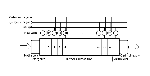
[0031] FIG. 1 is a schematic structural diagram of a vapor
deposition furnace according
to some embodiments of the present application.
DETAILED DESCRIPTION
[0032] The following description provides specific application
scenarios and
requirements of the present application in order to enable a person skilled in
the art to make and
use the present application. Various modifications to the disclosed
embodiments will be apparent
to a person skilled in the art. The general principles defined herein may be
applied to other
embodiments and applications without departing from the spirit and scope of
the present
application. Therefore, the present application is not limited to the
embodiments described
herein, but the broadest scope consistent with the claims.
[0033] The technical solution of the present application will be
described in detail below
with reference to the embodiments and accompanying drawings.
[0034] The present application provides a method for preparing a
silicon-based anode
material, comprising: passing a silicon substrate material through a vapor
deposition gas to coat a
surface of the silicon substrate material with a carbon deposition layer of a
certain thickness,
wherein the vapor deposition gas includes a first carbon source gas and a
second carbon source
gas, wherein, volume percentage of the first carbon source gas and the second
carbon source gas
CA 03203562 2023- 6- 27
in the vapor deposition gas increases or decreases at different reaction
stages for forming the
carbon deposition layer, a side of the carbon deposited layer close to the
silicon base material is
more or less dense than the other side of the carbon deposited layer.
[0035] In some embodiments of the present application, by way of
the method for
preparing the silicon-based anode material, the silicon substrate material can
be pulverized into
powdery particles, and the powdery particles are then transported to a vapor
deposition furnace.
The silicon substrate materials can be one or more of metallurgical silicon,
silicon oxide SiOx
(0<x<1.5), porous silicon, etc. The median diameter of the silicon substrate
material ranges from
1 gm to 20 gm. The silicon substrate material also includes a compound of the
general formula
MSiOy, where 0.85 <y<3; M can be any one or more of Li, Na, Mg, Al, Fe, and
Ca.
[0036] In the embodiments of the present application, the
particle size of the silicon
substrate material also has a certain influence on the electrochemical
performance of the finally
formed silicon-based anode material. As the particle size of the silicon
substrate material
decreases, and its specific surface area increases, the surface reaction that
accompanies the
charging and discharging cycles increases, and the formation of SET film
consumes more Lit,
which reduce the cycle characteristics and first cycle Coulombic efficiency of
the silicon-based
anode material. An increase in the particle size of the silicon substrate
material can prevent the
active material in the electrode from cracking due to charging and
discharging, which makes it
difficult to generate a new surface. Therefore, the amount of side reactions
is reduced, and the
cycle performance and first cycle Coulombic efficiency become better.
[0037] In the case where a chemical vapor deposition reaction is
performed in a vapor
deposition furnace, the volume percentage of the first carbon source gas and
the second carbon
source gas in the vapor deposition gas is highly related to the density of the
carbon deposition
layer formed. When the volume percentage of the first carbon source gas and
the second carbon
source gas decreases, the density of the formed carbon deposition layer
increases. Thus, the
carbon deposition layer can better suppress the expansion effect of the
internal core structure,
which is beneficial to the improvement of the electrochemical cycle
performance of the silicon-
based anode material. In addition, the smooth and dense carbon deposition
layer can facilitate the
formation of a stable SET film, which helps improve the first cycle Coulombic
efficiency. As the
volume percentage of the first carbon source gas and the second carbon source
gas increases, the
density of the formed carbon deposition layer decreases, and the interface
conductivity of the
6
CA 03203562 2023- 6- 27
carbon deposition layer increases. In some embodiments, the first carbon
source gas can be
acetylene, ethylene or a combination thereof, and the second carbon source gas
can be benzene,
toluene or a combination thereof
[0038] In some embodiments of the present application, when the
chemical vapor
deposition reaction is carried out, the volume percentage of the first carbon
source gas and the
second carbon source gas may increases or decreases in different reaction
stages in order to
adjust the density distribution of the formed carbon deposition layer. For
example, the volume
percentage of the first carbon source gas and the second carbon source gas may
be increased in a
stage, then decreased in the subsequent stage, and then increased again in the
next stage, so that a
carbon deposition layer with alternating density distributions may be formed.
In the
embodiments of the present application, the volume percentage of the first
carbon source gas and
the second carbon source gas in the vapor deposition gas may increase or
decrease within a range
of 0-20.
[0039] In some embodiments, the volume percentage of the first
carbon source gas and
the second carbon source gas in the vapor deposition gas monotonously
increases or decreases at
different reaction stages for forming a carbon deposition layer. That is to
say, the volume
percentage of the first carbon source gas and the second carbon source gas can
be adjusted
continuously or intermittently according to the setting, so as to form a
carbon deposition layer
whose density is continuously increased or discontinuously increased, or
carbon deposition layer
whose density is continuously decreased or discontinuously decreased. For
example, the volume
percentage of the first carbon source gas and the second carbon source gas in
the vapor
deposition gas monotonously increases or decreases between 0-20.
[0040] In some embodiments, the volume percentage of the first
carbon source gas and
the second carbon source gas in the vapor deposition gas increases or
decreases in a stepped
manner at different reaction stages for forming the carbon deposition layer.
As a result, the
density of the formed carbon deposition layer also increases or decreases in a
stepped manner.
For example, the volume percentage of the first carbon source gas and the
second carbon source
gas in the vapor deposition gas decreases from 5-20 in a gradient manner to 0-
5 or increases
from 0-5 to 5-20 in a gradient manner. Optionally, in some embodiments, the
volume percentage
of the first carbon source gas and the second carbon source gas in the vapor
deposition gas
decreases monotonically through 3 to 15 steps.
7
CA 03203562 2023- 6- 27
[0041] The changes in the density of the carbon deposition layer
also affect the
electrochemical performance of the silicon-based anode material. The changes
in the density of
the carbon deposition layer cause the carbon deposition layer structure to
contain certain sub-
structures. The more times the volume percentage of the first carbon source
gas and the second
carbon source gas change, the more sub-layers are included in the carbon
deposition layer
structure. As the number of structural sub-layers of the carbon deposition
layer increases, the
cycle performance of the silicon-based anode material becomes better.
[0042] A large change in the volume percentage of the first
carbon source gas and the
second carbon source gas would result in more significant sub-layered
structure formed in the
carbon deposition layer. Optionally, the carbon deposition layer structure
includes 3 to 15 sub-
layers, and the thickness of each sub-layer is the same or similar.
[0043] FIG. 1 is a schematic structural view of a vapor
deposition furnace according to
some embodiments of the present application. As shown in FIG. 1, the silicon
substrate material
is pulverized into powdery particles, and the powdery particles are then
transported through the
feeding zone to reach a heating zone in the vapor deposition furnace. The
powdery particles are
heated to a first temperature in the heating zone, for example, 700 C to 1000
C. After the heating
treatment, the powdery particles are transported to a thermal insulation zone,
where the thermal
insulation zone further includes n stages of reaction zones with independently
controlled
atmosphere, as shown in FIG. 1, the first furnace zone, the second furnace
zone, the third furnace
zone, the fourth furnace zone, the fifth furnace zone, ... the n-lth furnace
zone, nth furnace zone.
Different reaction areas correspond to different reaction stages during the
forming process of the
carbon deposition layer. In some embodiments, the thermal insulation zone may
be equally
divided into n sections with equal lengths, or may be divided into n sections
with unequal
lengths. The value of n can be, for example, 3-15.
[0044] For each reaction zone, the atmosphere may include a
first carbon source gas
(corresponding to the carbon source A shown in FIG. 1), a second carbon source
gas
(corresponding to the carbon source B shown in FIG. 1), and an inert gas. The
first carbon source
gas may be one or a combination of acetylene and ethylene. The second carbon
source gas may
be one or a combination of benzene and toluene. The inert gas may be one or a
combination of at
least two of argon, nitrogen and helium. The total volume of the first carbon
source gas and the
second carbon source gas accounts for 1-30% of the total volume percentage of
the atmosphere.
8
CA 03203562 2023- 6- 27
[0045] The volume percentage of the first carbon source gas and
the second carbon
source gas in the vapor deposition gas increases or decreases at different
reaction stages for
forming the carbon deposition layer. The the volume ratio of the first carbon
source gas to the
second carbon source gas in the total atmosphere volume of each section of the
heat preservation
zone is referred to as R, then R would decrease or increase from R1 in the
first furnace zone to
Rn in the nth furnace zone as required. For example, R1 in the first furnace
zone is 19, R2 in the
second furnace zone is 17, R3 in the third furnace zone is 14, R4 in the
fourth furnace zone is 12,
R5 in the fifth furnace zone is 8, and R6 in the sixth furnace zone is 6.
[0046] In some embodiments, the volume percentage of the first
carbon source gas and
the second carbon source gas in the vapor deposition gas may monotonously
increase or
decreases at different reaction stages for forming a carbon deposition layer.
The volume
percentage of the first carbon source gas and the second carbon source gas may
monotonically
increase or decrease between 0-20. For example, R1 in the first furnace zone
is 15, R2 in the
second furnace zone is 12, R3 in the third furnace zone is 9, R4 in the fourth
furnace zone is 6,
and so on. For another example, R1 in the first furnace zone is 6, R2 in the
second furnace zone
is 9, R3 in the third furnace zone is 12, R4 in the fourth furnace zone is 15,
and so on.
[0047] In some embodiments, the volume percentage of the first
carbon source gas and
the second carbon source gas in the vapor deposition gas may increase or
decrease monotonously
in a stepped manner in different reaction stages for forming the carbon
deposition layer. The
volume percentage of the first carbon source gas and the second carbon source
gas may change
between 0 and 20, that is, 0<R<20. For example, the volume percentage of the
first carbon
source gas and the second carbon source gas in the vapor deposition gas may
decrease in a
gradient manner from 5-20 to 0-5, or increase in a gradient manner from 0-5 to
5-20. In the vapor
deposition gas, the volume percentages of the first carbon source gas and the
second carbon
source gas may decrease monotonically according through 3 to 15 steps. Since
the thermal
insulation zone can be divided into a plurality of reaction zones (for
example, 3 to 15 reaction
zones) that can independently control the atmosphere, the volume percentages
of the first carbon
source gas and the second carbon source gas can be regarded as uniform and
unchanged in the
same reaction zone, and can increase or decrease monotonously between
different reaction areas.
For example, R1 in the first furnace zone is 15, R2 in the second furnace zone
is 12, R3 in the
third furnace zone is 9, R4 in the fourth furnace zone is 6, and so on. For
another example, R1 in
9
CA 03203562 2023- 6- 27
the first furnace zone is 6, R2 in the second furnace zone is 9, R3 in the
third furnace zone is 12,
R4 in the fourth furnace zone is 15, and so on.
[0048] The temperature of the vapor deposition heat treatment in
the thermal insulation
zone is from 700 C to 1000 C, and the treatment time is from 3 to 12 hours.
After the powder
material is vapor-deposited and coated, the silicon-based anode material with
a carbon deposition
layer have a surface for changes structure can be obtained after cooling down
to room
temperature under an inert gas condition. The thickness of the carbon
deposition layer can be
from 10 nm to 150 nm.
[0049] Through the chemical vapor deposition reaction, by means
of adjusting the staged
atmosphere conditions in the vapor deposition reaction furnace, the present
application can
control the heat treatment time of the reactants under different atmosphere
conditions, and
achieve the preparation of a silicon material coated with a carbon deposition
layer with structural
changes on the surface thereof. The carbon deposition layer is tightly coated,
which can
effectively suppress the volume effect and conductivity of the silicon-based
anode material
during the battery charging and discharging processes, and thus greatly
improve the cycle
stability of the material.
[0050] The embodiments of the present application further
provide a silicon-based anode
material prepared according to the preparation method of a silicon-based anode
material as
provided by the present application. Since the gas composition changes in a
stepped manner
during the vapor deposition process, the carbon deposition layer formed will
also have structural
changes. The silicon-based anode material provided by the present application
may include a
silicon substrate material and a carbon deposition layer, the carbon
deposition layer covers the
silicon substrate material, where the side of the carbon deposition layer
close to the silicon
substrate material is more or less dense than the other side of the carbon
deposition layer. The
silicon substrate material may include one or more of metallurgical silicon,
silicon oxide SiOx
(0<x<1.5), and porous silicon, and the median diameter of the silicon
substrate material ranges
from 1 gm to 20 Am.
[0051] In some embodiments, the density of the carbon deposition
layer may increases
or decreases monotonously from an inner side thereof to an outer side thereof.
Since the volume
percentage of the first carbon source gas and the second carbon source gas in
the vapor
deposition gas increases or decreases at different reaction stages for forming
the carbon
CA 03203562 2023- 6- 27
deposition layer, the density of the carbon deposition layer formed under
different gas volume
ratios may also be different. The density of the carbon deposition layer may
increase or decrease
from the inner side to the outer side as the volume percentage of the first
carbon source gas and
the second carbon source gas changes.
[0052] In some embodiments, the density of the carbon deposition
layer may increase or
decrease monotonously through 3 to 15 steps. Since the thermal incubation zone
can be divided
into a plurality of reaction zones (for example, 3 to 15 reaction zones) that
can independently
control the atmosphere, the volume percentage of the first carbon source gas
and the second
carbon source gas can be regarded as uniform and unchanged in the same
reaction zone, and may
increase or decrease monotonously between different reaction areas. The
density of the carbon
deposition layer formed in the same reaction area can be regarded as
approximately unchanged
or slightly changed, and the density of the carbon deposition layer formed in
different reaction
areas can be regarded as having an increasing or decreasing trend.
[0053] The present application will be described in more detail
in reference to Examples
1 to 6 provided below.
[0054] Example 1
[0055] (1) Silicon oxide SiO particles are crushed to D50 = 8 m
by mechanical grinding.
[0056] (2) The powder obtained in step (1) is loaded in a vapor
deposition furnace for a
vapor deposition coating treatment. The thermal insulation zone in the vapor
deposition furnace
has 12 sections with independently controlled atmosphere, and the atmosphere
condition is a
mixed gas of argon, ethylene and benzene. Ethylene and benzene are vapor
deposition gases, and
a total volume of the two vapor deposition gases accounts for 8% of the total
gas volume (the
total gas volume is the sum of the volumes of argon, ethylene and benzene).
Table 1 shows the
composition and corresponding R values of the 12 different stages of furnace
atmosphere in the
thermal insulation zone. The vapor deposition temperature is 950 C, and the
axial speed of the
material is adjusted so that the time for the powder to pass through the
thermal insulation zone is
6 hours. After a sample is vapor-deposited and coated, the temperature is
reduced to room
temperature under nitrogen to obtain a silicon-based anode material with a
carbon deposition
layer of continuous structural changes on the surface.
Table 1
Gas content Thermal insulation zone
11
CA 03203562 2023- 6- 27
in volume 1 2 3 4 5 6 7 8 9 10
11 12
percentage
1%
Ethylene 7.50 7.50 7.50 7.50 7.38 7.20 6.86 6.00 6.00 6.00 6.00
6.00
Benzene 0.50 0.50 0.50 0.50 0.62 0.80 1.14 2.00 2.00 2.00 2.00
2.00
R 15 15 15 15 12 9 6 3 3 3 3 3
[0057] Example 2
[0058] (1) Silicon oxide SiO particles are crushed to D50 = 8 gm
by mechanical
grinding.
[0059] (2) The powder obtained in step (1) is loaded in a vapor
deposition furnace for a
vapor deposition coating treatment. The thermal insulation zone in the vapor
deposition furnace
has 12 sections with independently controlled atmosphere, and the atmosphere
condition is a
mixed gas of argon, ethylene and toluene. Ethylene and toluene are vapor
deposition gases, and a
total volume of the two vapor deposition gases accounts for 10% of the total
gas volume. Table 2
shows the composition and corresponding R values of the 12 different stages of
furnace
atmosphere in the thermal insulation zone. The vapor deposition temperature is
950 C, and the
axial speed of the material is adjusted so that the time for the powder to
pass through the thermal
insulation zone is 6 hours. After a sample is vapor-deposited and coated, the
temperature is
reduced to room temperature under nitrogen to obtain a silicon-based anode
material with a
carbon deposition layer of continuous structural changes on the surface.
Table 2
Gas content Thermal insulation zone
in volume 1 2 3 4 5 6 7 8 9 10
11 12
percentage
1%
Ethylene 9.37 9.37 9.37 9.37 9.23 9.00 8.57 8.00 6.67 6.67 6.67
6.67
Toluene 0.63 0.63 0.63 0.63 0.77 1.00 1.43 2.00 3.33 3.33 3.33
3.33
R 15 15 15 15 12 9 6 4 2 2 2 2
[0060] Example 3
[0061] (1) Silicon oxide SiO particles are crushed to D50 = 8 gm
by mechanical
grinding.
[0062] (2) The powder obtained in step (1) is loaded in a vapor
deposition furnace for a
vapor deposition coating treatment. The thermal insulation zone in the vapor
deposition furnace
12
CA 03203562 2023- 6- 27
has 12 sections with independently controlled atmosphere, and the atmosphere
condition is a
mixed gas of argon, acetylene and benzene. Acetylene and benzene are vapor
deposition gases,
and a total volume of the two vapor deposition gases accounts for 10% of the
total gas volume.
Table 3 shows the composition and corresponding R values of the 12 different
stages of furnace
atmosphere in the thermal insulation zone. The vapor deposition temperature is
950 C, and the
axial speed of the material is adjusted so that the time for the powder to
pass through the thermal
insulation zone is 6 hours. After a sample is vapor-deposited and coated, the
temperature is
reduced to room temperature under nitrogen to obtain a silicon-based anode
material with a
carbon deposition layer of continuous structural changes on the surface.
Table 3
Gas content Thermal insulation zone
in volume 1 2 3 4 5 6 7 8 9 10
11 12
percentage
1%
Acetylene 9.00 9.00 9.00 9.00 8.57 8.57 7.50 7.50 6.00 6.00 6.00 6.00
Benzene 1.00 1.00 1.00 1.00 1.43 1.43 2.50 2.50 4.00 4.00 4.00
4.00
R 9 9 9 9 6 6 3 3 1.5 1.5 1.5 1.5
[0063] Example 4
[0064] (1) Silicon oxide SiO particles are crushed to D50 = 2.5
m by mechanical
grinding.
[0065] (2) The powder obtained in step (1) is loaded in a vapor
deposition furnace for a
vapor deposition coating treatment. The thermal insulation zone in the vapor
deposition furnace
has 12 sections with independently controlled atmosphere, and the atmosphere
condition is a
mixed gas of argon, ethylene and benzene. Ethylene and benzene are vapor
deposition gases, and
a total volume of the two vapor deposition gases accounts for 16% of the total
gas volume. Table
4 shows the composition and corresponding R values of the 12 different stages
of furnace
atmosphere in the thermal insulation zone. The vapor deposition temperature is
850 C, and the
axial speed of the material is adjusted so that the time for the powder to
pass through the thermal
insulation zone is 6 hours. After a sample is vapor-deposited and coated, the
temperature is
reduced to room temperature under nitrogen to obtain a silicon-based anode
material with a
carbon deposition layer of continuous structural changes on the surface.
Table 4
13
CA 03203562 2023- 6- 27
Gas Thermal insulation zone
content 1 2 3 4 5 6 7 8 9 10 11
12
in
volume
percent
age 1%
Ethylen 15.0 15.0 15.0 15.0 15.0 15.0 14.7 14.4 13.7 12.0 12.0 12.0
e 0 0 0 0 0 0 7 0 1 0
0 0
Benzen 1.00 1.00 1.00 1.00 1.00 1.00 1.23 1.60 2.29 4.00 4.00 4.00
e
R 15 15 15 15 15 15 12 9 6 3
3 3
[0066] Example 5
[0067]
(1) Silicon oxide SiO particles are crushed to D50 = 2.5 m by mechanical
grinding.
[0068] (2) The powder obtained in step (1) is loaded in a vapor
deposition furnace for a
vapor deposition coating treatment. The thermal insulation zone in the vapor
deposition furnace
has 12 sections with independently controlled atmosphere, and the atmosphere
condition is a
mixed gas of argon, ethylene and benzene. Ethylene and benzene are vapor
deposition gases, and
a total volume of the two vapor deposition gases accounts for 16% of the total
gas volume. Table
shows the composition and corresponding R values of the 12 different stages of
furnace
atmosphere in the thermal insulation zone. The vapor deposition temperature is
850 C, and the
axial speed of the material is adjusted so that the time for the powder to
pass through the thermal
insulation zone is 6 hours. After a sample is vapor-deposited and coated, the
temperature is
reduced to room temperature under nitrogen to obtain a silicon-based anode
material with a
carbon deposition layer of continuous structural changes on the surface.
Table 5
Gas Thermal insulation zone
content 1 2 3 4 5 6 7 8 9 10 11
12
in
volume
percent
age 1%
Ethylen 15.0 15.0 15.0 15.0 15.0 15.0 14.7 14.4 13.7 12.0 12.0 12.0
e 0 0 0 0 0 0 7 0 1 0
0 0
14
CA 03203562 2023- 6- 27
Benzen 1.00 1.00 1.00 1.00 1.00 1.00 1.23 1.60 2.29 4.00 4.00 4.00
e
R 15 15 15 15 9 9 9 9 3 3 3
3
[0069] Example 6
[0070] (1) Silicon oxide SiO particles are crushed to D50 = 2.5
gm by mechanical
grinding.
[0071] (2) The powder obtained in step (1) is loaded in a vapor
deposition furnace for a
vapor deposition coating treatment. The thermal insulation zone in the vapor
deposition furnace
has 12 sections with independently controlled atmosphere, and the atmosphere
condition is a
mixed gas of argon, acetylene and benzene. Acetylene and benzene. Ethylene and
benzene are
vapor deposition gases, and a total volume of the two vapor deposition gases
accounts for 10%
of the total gas volume. Table 6 shows the composition and corresponding R
values of the 12
different stages of furnace atmosphere in the thermal insulation zone. The
vapor deposition
temperature is 850 C, and the axial speed of the material is adjusted so that
the time for the
powder to pass through the thermal insulation zone is 6 hours. After a sample
is vapor-deposited
and coated, the temperature is reduced to room temperature under nitrogen to
obtain a silicon-
based anode material with a carbon deposition layer of continuous structural
changes on the
surface.
Table 6
Gas content Thermal insulation zone
in volume 1 2 3 4 5 6 7 8 9 10
11 12
percentage
1%
Acetylene 9.00 9.00 9.00 9.00 9.00 9.00 7.50 7.50 7.50 6.00 6.00 6.00
Benzene 1.00 1.00 1.00 1.00 1.00 1.00 2.50 2.50 2.50 4.00 4.00
4.00
R 9 9 9 9 9 9 3 3 3 1.5 1.5 1.5
[0072] The silicon-based anode material samples obtained in the
above Examples 1 to 6
are then made into button batteries using a lithium sheet as a counter
electrode, and the charge
cycle test is next performed. The charge and discharge rate was 0.1C, and the
charge and
discharge voltage range is from 0.01 V to 1.50 V. The test results obtained
are shown in Table 7
below.
Table 7
CA 03203562 2023- 6- 27
Sample First cycle specific First cycle
Coulombic Capacity retention
discharge capacity efficiency rate after 10
cycles
Example 1 1660.1 76.3% 78.4%
Example 2 1645.4 76.7% 80.9%
Example 3 1670.3 77.5% 71.5%
Example 4 1464.3 74.6% 68.8%
Example 5 1476.8 74.3% 64.7%
Example 6 1512.4 73.5% 57.6%
[0073] It can be seen from the test data shown in Table 7 that
in Examples 1 to 3, the
volume percentages of the first carbon source gas and the second carbon source
gas decrease
sequentially; as a result, the density of the formed carbon deposition layer
increases sequentially,
and the effect of inhibiting the expansion of the internal core structure is
also more significantly
in this order, which is beneficial to the improvement of the cycle
performance. The smooth and
dense carbon deposition layer is beneficial to the formation of a stable SET
film, which is further
beneficial to improve the Coulombic efficiency.
[0074] Moreover, in Example 2, as the number of sub-layer
structures in the carbon
deposition layer increases, the cycle performance of the silicon-based anode
material becomes
better. In Example 3, the volume percentage content of the second carbon
source gas benzene
accounts for a relatively larger percentage. As a result, a smooth and dense
carbon deposition
layer is formed, which is beneficial to the formation of an SET film. Thus, it
first cycle
Coulombic efficiency has been improved to some extent, but its carbon
deposition layer has
fewer sub-layer structures, accordingly, its cycle performance is reduced
compared to that of
Example 2. Compared with Example 2, both the carbon content and the number of
sub-layer
structures in the carbon deposition layer in Example 1 are slightly lower,
accordingly, its capacity
is improved, but the cycle number is slightly reduced.
[0075] In Examples 5 and 6, the cycle performance of the silicon-
based anode material is
lower than those of Examples 1 to 3; this is due to the fact that the median
diameter of their
silicon substrate material particles has been changed. When the median
diameter of the anode
active material particle is 2.5 gm, the specific surface area increases, so
the surface reaction
accompanying the charge and discharge cycles increases, and the formation of
the SET film
would consume more Lit, thereby reducing the cycle characteristics and the
first cycle
Coulombic efficiency. When the median particle size is 8 gm, it can prevent
the active material
16
CA 03203562 2023- 6- 27
from cracking during the charging and discharging processes and thus the newly
formed new
surface is reduced. As a result, the amount of side reactions is reduced, and
the cycle
performance and first cycle Coulombic efficiency are improved. When comparing
Example 5
with Example 6, the number of carbon sub-layer structures in Example 5 is
higher than that in
Example 6, and thus its cycle performance is better. In Example 6, because the
median particle
size of the silicon-based material is 2.5 i.tm, its specific surface area is
larger, 10% volume
fraction of carbon source coating results in low carbon content, further it
has a lower number of
carbon sub-layer structures. As a result, it has poorer cycle performance and
lower first cycle
Coulombic efficiency. However, since its Si/C ratio is higher as compared to
Examples 4 and 5,
its capacity has been increased accordingly.
[0076] In summary, after reading the detailed disclosure
provided above, a person skilled
in the art will understand that the disclosures are merely some example, and
do not limit the
present application. Moreover, although not explicitly stated herein, a
skilled in the art will
understand that the present invention is intended to cover various changes,
modifications and
improvements of the embodiments. These changes, modifications and improvements
are
intended to be proposed in the present application and are within the spirit
and scope of the
exemplary embodiments of the present application.
[0077] It will be appreciated by a person of ordinary skill in
the art that the term "and/or"
used herein includes any and all combinations of one or more of the related
items listed.
[0078] It will also be appreciated by a person of ordinary skill
in the art that the terms
"comprise", "comprising", "include" and/or including, when used herein, refer
to the presence of
stated features, entities, steps, operations, elements and/or assemblies, but
do not exclude the
presence or addition of one or more other features, entities, steps,
operations, elements,
assemblies and/or combinations thereof.
[0079] It should also be understood that although the terms
"first", "second", "third", etc.
may be used herein to describe various elements, these elements may not be
limited by these
terms. These terms are merely used to distinguish one element from another.
Thus, a first
element in some embodiments may be referred to as a second element in other
embodiments
without departing from the teachings of the present application. Moreover, the
same reference
symbols or reference numerals are used throughout entire disclosure to
represent the same
elements.
17
CA 03203562 2023- 6- 27
[0080]
Furthermore, the exemplary embodiments are described by referring to the
cross
sectional and/or planar illustrations as the idealized exemplary illustration.
18
CA 03203562 2023- 6- 27