Note: Descriptions are shown in the official language in which they were submitted.
-1 -
TP0445
Definition
Title
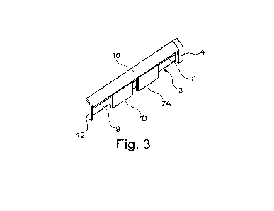
Bus system and support device comprising such a bus system
Description
Technical field
The invention relates to a bus system comprising lines and a supply device for
supplying devices with electric power and for the communication supply of
these devices, bus-system compatible devices and a support device
comprising such a bus system.
Background
WO 2017/153481 Al discloses a support device in the form of a
shelf edge strip (sometimes termed shelf rail), which comprises a base
support which is designed for mechanically fastening an electronic display
unit. The base support delimits an accommodating region for accommodating
the display unit, comprising three side walls, which are arranged in a U-
shape. Thus, the accommodating region is delimited on three sides here and
the display unit can be inserted into the shelf edge strip or removed
therefrom from the front, via the side of the U shape which is left open.
A first, central side wall is formed by a plate. This plate is used as a
reference or positioning plane, on which the rear wall of the display unit can
be positioned on the shelf edge strip. The plate comprises openings, which
are arranged in a grid. These openings are used for contacting electrical
conductor tracks by means of contact pins of the display unit, in order to
supply the display unit electrically. The conductor tracks are arranged on a
conductor support, which is positioned on the side of the first side wall
which
faces away from the accommodating region.
The support device also comprises a supply device, which supplies
the display unit both in terms of communication and with electric power. The
CA 03205623 2023- 7- 19
- 2 -
supply device is electrically conductively connected to the conductor tracks,
carries the batteries required for battery operation and is arranged behind
the
conductor support. A bus system for this support device is formed here by the
combination of supply device and conductor tracks.
This bus system is designed exclusively for operation with a single
type of device, namely the display units, which comprise screens with an
extremely low energy requirement, which is enabled for example by the use
of "electronic ink" technology.
Against this background, the object of the invention is to provide an
improved bus system.
Summary of the Invention
This object is achieved by a bus system according to Claim 1. The
subject matter of the invention is therefore a bus system, a shelf edge strip
bus system in particular, which comprises: a first line for determining an
electric reference potential, a second line for providing a supply voltage
with a
desired value in relation to the reference potential, at least one third line,
preferably a single third line, for communication of signals and/or data, and
a
supply device, which is electrically conductively connected to the lines and
is
designed for electric power supply as well as for communication supply of
electronic devices which can be connected to the bus system, wherein the
supply device is designed to supply different device types both with electric
power and, following the identification thereof, with communication in a
device-type-specific manner.
Furthermore, this object is achieved by an electronic device
according to Claim 16. The subject matter of the invention is therefore an
electronic device, which device comprises a bus interface, which is designed
for connection to lines of a bus system, wherein the bus system comprises: a
first line for determining an electric reference potential, a second line for
providing a supply voltage in relation to the reference potential, at least
one
third line, preferably a single third line, for communication of signals
and/or
data, and a supply device, which is electrically conductively connected to the
lines and is designed for electric power supply as well as for communication
supply of electronic devices which can be connected to the bus system,
wherein the device is designed for the identification of the device with
respect
CA 03205623 2023- 7- 19
- 3 -
to the supply device for the purpose of subsequent device-type-specific
communication with the supply device.
Furthermore, this object is achieved by a support device according
to Claim 34. The subject matter of the invention is therefore a support
device,
preferably a shelf edge strip, which comprises a bus system according to the
invention.
The measures according to the invention are associated with the
advantage that, in a departure from the known bus system, devices of a very
wide range of types can now be operated on the support device. This allows a
substantially more flexible equipment of the support device with devices,
which may differ with regards to their type (that is to say e.g. due to the
device class), such as e.g. electronic display units, sensor units, input
units or
else image-capturing units, etc., thus the functionality of the support device
can de facto be extended as desired or else adapted to individual
requirements.
Devices of a very wide range of types may however also exist within
a device class, such as e.g. the device class electronic display units. These
display units may differ with regards to their type due to the screen diagonal
or else due to the number of pixels or the range of colours that can be
displayed or else due to the technology used (electrophoretic, OLED or LCD,
etc.), etc. The situation is similar for the device class of the image-
capturing
units. These image-capturing units may differ with regards to the type of the
result of their image capture, namely still image or video stream or else with
regards to the resolution or else the spectral range, etc. All these
differences
within a device class may make a device-type-specific activation or
communication necessary, in order to be able to use the very wide range of
functionalities optimally.
The usability of devices of different types is actually achieved by
means of two measures, which mesh with one another.
The first measure stems from the supply device being designed to
communicate with different device types, particularly in a device-type-
specific
manner. This may be realized by storing communication parameterizations,
such as communication protocols and/or instruction sets, for different device
types, which pararneterizations can be retrieved or used in a flexible manner.
In this case, these communication parametrizations may e.g. be saved in the
CA 03205623 2023- 7- 19
- 4 -
supply device in advance or may be retrievable by the supply device as
required from a device management server. This communication
parameterization could also be provided directly by the relevant electronic
device. It may also be provided that the provision of supply voltage or the
supply power is adapted by the supply device in a device-type-specific
manner.
The second measure stems from each device being designed for its
identification with respect to the supply device, particularly across device
types or independently of device type, before the device can be used for
device-type-specific communication with the supply device; this is also
discussed in detail in the following, particularly in connection with the
acquisition of identification data by the supply device and the delivery of
the
identification data by the electronic device. During this device-type-
independent identification, the said identification data are transmitted,
which
subsequently allow a device-type-specific communication between the supply
device and the respective device.
Further particularly advantageous embodiments and developments
of the invention result from the dependent claims and also the following
description.
Details of the setup of the communication as well as the
communication handling in the bus system are discussed in the following.
One of these aspects relates to the introduction of a change of an
operating state or mode. It has proven advantageous here that the supply
device is designed for a temporary change of the supply voltage, in order to
introduce a change of an operating mode. On the part of the electronic
device, it is provided that the device comprises a detection stage, which is
designed for detecting a temporary change of the supply voltage, and that
the device is designed to change its operating mode in the event of such a
detection.
These measures are associated with the advantage that, in contrast
to known bus systems, the signalling of a change of the operating mode no
longer necessarily has to take place by means of separate signal or data lines
which are specially provided therefor. Rather, the line provided for the
electric
power supply is used, without using the at least one third line, which is
provided for the signal and/or data communication. Therefore, it is also not
CA 03205623 2023- 7- 19
- 5 -
necessary that the devices connected to the bus are in a synchronous state
with the supply device at the time of the introduction of the change of the
operating state. Rather, each device may be in any desired, device-specific
operating mode, such as a sleep or idle mode with low to essentially no power
consumption or else a processing or active mode, in which an autonomous
processing of information, signals and/or data takes place in the device. The
same also applies otherwise for the supply device. That a change of an
operating mode is now being introduced or at least has already been
introduced on the part of the supply device is signalled or communicated by
the supply device to the electronic devices connected to the bus system with
the aid of a temporary change of the supply voltage and is detected and, if
appropriate, also implemented there.
In this case, the change of an operating mode may exclusively be a
change of the supply device operating mode. In this case, this supply device
operating mode change is simply only shared with the other devices, in order
to inform the devices of this. The thus-informed devices can remain in their
own operating mode pattern and in principle in no way have to react or show
a reaction outwardly.
The change of an operating mode may however also be a change of
a device operating mode, which is sought by the supply device and is to be
introduced at the devices e.g. in a manner unaffected by the respective
currently present supply device operating mode. In this case, the requirement
of device operating mode change is shared with the devices, detected and
also implemented there.
The change of an operating mode may however also be a collective
change of the supply device operating mode and the device operating mode.
In this case, the requirement of a change of the operating mode with bus-
system-wide validity as it were is signalled or communicated and all of the
devices connected to the bus system follow this request by the supply device
and introduce the change of their device operating mode, in order e.g. to be
consistent with the supply device operating mode, which is likewise
introduced. This can also be understood as a synchronization of the currently
present device-specific operating modes between the supply device and the
devices connected to the bus system.
CA 03205623 2023- 7- 19
- 6 -
This measure supports the flexibility of the bus system to operate
and to activate an almost arbitrary range of different devices or device types
using the bus system, specifically primarily without the absolute necessity of
having to take account of special communication protocols or functional
characteristics of the individual devices. In stark contrast to known
measures,
in which an operating mode change must be communicated by means of data
communication according to a communication protocol adapted to the devices
which are connected to the bus system, the invention makes use of those
lines of the bus system which are conventionally only provided for the
electrical supply, and indicates to the devices, which are connected to the
bus
system, by means of a temporary change of the supply voltage, that an
operating mode change is to be introduced.
This also allows, for the first time, the use of devices at the bus
system, which can be designed electronically (in terms of circuitry) such that
the devices are decoupled or separate from the at least one third line,
wherein the devices are, in spite of this, supplied with electric power via
the
first and the second line. In spite of the decoupling from the at least one
third
line, the devices which are connected to the bus system remain reachable for
the supply device in terms of communication or signal technology and the
devices can be supplied with "basic information", such as in the current
context, the control information, that a change of the operating mode is to be
introduced.
The multiplicity of different devices, which has already been
mentioned previously, may, without claiming an exhaustive list, comprise a
basic functionality or basic design: Sensors, such as e.g. temperature sensors
or proximity sensors, etc., cameras for still image capture or video capture
or
infrared capture; input devices such as e.g. individual keys or keypads or
rotary knobs or rotary controls or else touchscreens; display units, such as
e.g. one or more light-emitting diodes (LEDs), video screens or else
electronic
shelf displays with energy-saving bistable screen technologies, such as e.g.
electronic ink or e-paper or active screen technologies, such as e.g. liquid
crystal display (LCD) or organic light-emitting diodes (OLEDs), etc.
All of these different devices are designed in a manner compatible
with the bus system of the support device, in order to be connected to the
bus system and used there.
CA 03205623 2023- 7- 19
- 7 -
The aforementioned devices therefore essentially have a basic
functionality. Such devices may however also have combined basic
functionalities or provide a dominant basic functionality which is extended by
further supporting functions. Thus, these devices may also provide further,
supplementary communication functionalities, such as e.g. an NFC interface
for device activation, for data transmission from and to the device or else
control of functions of the device from the direct vicinity (a few millimetres
to
a few centimetres) or else for producing a link between a product and the
electronic device or a Bluetooth low-energy radio module for wireless
communication over wider distances with compatible devices.
Each of these devices comprises device electronics, which can be
divided structurally as well as functionally into different circuit blocks.
Thus,
the device electronics may comprise at least one circuit block for the
respective basic functionality, if appropriate also one circuit block for the
additional functionality, one circuit block for the energy supply and at least
one circuit block for coupling to the bus system, if appropriate separated
into
coupling to the at least one third line on the one hand and coupling to the
second line on the other hand.
Different tasks or roles may be assigned to the supply device,
depending on the context in which the bus system is used.
One of these roles consists in the fundamental task of the electrical
supply of the devices connected to the bus system. For this purpose, the
supply device itself can be electrically supplied with the aid of a local or
central power supply unit or else supplied via radio, such as e.g. using power
over WiFi technology. The supply device can also be connected to a
(rechargeable) battery which is assigned to it, from which the supply device
draws the electric power for its own operation as well as for the operation of
the devices which are connected to the bus system.
A further role consists, with the aid of the supply voltage, in
introducing a change of an operating mode. This may e.g. be necessary if the
supply device is used as a shelf edge strip controller on a shelf edge strip
which carries the lines, if a central management instance (e.g. a cloud
service
or a local server where a management software - also termed a
superordinate "software entity" - is executed for managing electronic devices
which are fastened to the shelf edge strip) must identify the individual
CA 03205623 2023- 7- 19
- 8 -
devices on the shelf edge strip, retrieve the data of the individual devices
or
else activate or supply the individual devices with data. Here, the supply
device may also, even already in advance of the actual communication with
the central management instance, proactively carry out the detection of the
devices installed on the shelf edge strip, store the thus-detected
identification
data and only deliver these identification data to the central management
instance at a later time.
The cloud service is connected via the Internet to a local LAN or
WLAN infrastructure, wherein one or more access points provide the
connection to the supply devices in this infrastructure.
The local server may also be connected to such access points via a
LAN or WLAN infrastructure.
Each access point can be designed to communicate with the supply
device via a wireless connection. In this case, a (de facto) standardized
communication method (e.g. ZigBee C), Bluetooth Low Energy, WLAN, etc.)
or a proprietary communication method can be used. A proprietary
communication method of this type is for example known from
WO 2015/124197 Al, the disclosure of which is hereby included by reference.
In contrast to WO 2015/124197 Al, the time slot communication method
disclosed there is not used in the present case in the devices which are
attached to the shelf edge strip, which devices are indeed connected to the
supply device in a wired manner, but rather is used in the supply device for
the communication with the access point. The systematic change - which is
disclosed in WO 2015/124197 Al in connection with the electronic display
units (referred to as radio tags there) - between an extremely energy-saving
sleep state and, in comparison thereto, an energy-consuming active state, in
order on the one hand to ensure operation which is as energy-saving as
possible and on the other hand to ensure synchronism with the access point,
is implemented in the present case in the supply device.
Independently of the choice of wireless communication method, a
group of supply devices can be assigned to an access point, which supplies
them in terms of radio technology, wherein each supply device supplies the
devices connected to its bus system in a wired manner. The respective supply
device therefore forms an access or control node for the devices which are
installed on its support device, such as e.g. its shelf edge strip.
CA 03205623 2023- 7- 19
- 9 -
In principle, it may be provided that the supply device always stays
in its extremely energy-saving sleep state if there is no activity
requirement.
The supply device also comprises supply device electronics, which
can be divided into circuit blocks. Thus, a circuit block is also provided
here
for the electrical supply of the supply device. This may be a voltage
regulator,
such as e.g. a series regulator, particularly an LDO linear regulator (LDO
stands for low dropout), which is connected to an internal or an external
energy storage device, which outputs a voltage of 3.7 to 4.2 volts (such as
e.g. a battery, a battery pack or a configuration of rechargeable battery
cells), and generates an internal supply voltage of the supply device with
approx. 3.3 volts.
A further circuit block may be a logic stage, which is realized in
particular with a microcontroller and which is operated with the aid of the
internal supply voltage. The microcontroller, if appropriate including its
peripherals, provides the various functionalities of the supply device, which,
with the exception of the hardware features, are realized with the aid of a
software which is executed by the microcontroller, is stored in a memory of
the microcontroller and, if appropriate, uses hardware features during its
execution.
A further circuit block may be a stage for generating the (external)
supply voltage for the second line of the bus system, wherein a step-up
converter may for example be used for this, which is connected at the input
side to the external energy storage device. At the output side, the step-up
converter generates the bus system supply voltage with the defined desired
value of e.g. 5 volts.
A further circuit block may be formed by a fault detection circuit,
which is designed for detecting faults on the at least one third line and
which
is connected between the at least one third line and the send and receive pins
of the microcontroller as well as an analogue/digital converter pin (ADC
input)
of the microcontroller. Using the ADC input, the microcontroller can also
detect, possibly measure or evaluate the voltage present on the at least one
third line. A further analogue/digital converter pin (ADC input) of the
microcontroller may also be connected directly to the second line, so that the
microcontroller can also detect, possibly measure or evaluate the voltage
present on the at least one third line.
CA 03205623 2023- 7- 19
- lo -
A further circuit block can be used for detecting an overload of the
bus system, caused in particular on the at least one third line, and is
configured such that when an overload is detected, the output of the step-up
converter is disconnected from the second line.
A further circuit block may relate to the radio system, which is used
for the radio traffic with the aforementioned access point. This circuit block
may comprise an antenna configuration as well as a matching network.
Likewise, a circuit is provided here for converting analogue signals received
via radio into digital signals and vice versa. This circuit block is connected
to
the microcontroller, so that the microcontroller can, in radio traffic with
the
access point, receive data and for its part deliver data to be transmitted via
radio signal.
Furthermore, a circuit block may be provided, which comprises a
signalling unit which can be activated by the microcontroller, in the simplest
case a single LED.
Furthermore, a circuit block may also be provided, which comprises
an input unit which can be read by the microcontroller, in the simplest case a
key.
A memory stage, in the present case for example a flash memory,
which can also be addressed by the microcontroller via an e.g. serial
peripheral interface (SPI for short), may also be provided as a further
circuit
block.
Also, when in the preceding text passages, the supply unit
electronics and the device electronics were explained conceptually on the
basis of circuit blocks, it may be noted at this point that the respective
electronics may also be realized as e.g. an ASIC (application specific
integrated circuit) or as a "system on a chip", so that the electronics may be
divided less into discrete circuit blocks and rather into functional units of
an
integrated circuit.
The external energy storage device may be a conventional battery
or a configuration of batteries or battery cells. However, it has proven
particularly advantageous if the supply device is coupled to an external
energy storage device for the purpose of electrically supplying the supply
device, wherein the external energy storage device is particularly preferably
a
"smart energy storage device" and the supply device is designed to receive
CA 03205623 2023- 7- 19
-11 -
and to process information or data, which relates to the energy-storage-
device type and/or the electrical storage capacity and/or the usage history
and/or the energy supply status, from the external energy storage device via
a data or signal line. The smart energy storage device may comprise an
internal battery microcontroller, which can be connected via its
communication interface, e.g. realized in accordance with the I2C or SMBUS
(system management bus) specification, to the supply device electronics,
which comprise a compatible communication interface, particularly to the
logic stage thereof, e.g. via a cable. With the aid of the battery
microcontroller, a very wide range of smart functions can be realized, which
may e.g comprise the precise detection of the charging or consumption state
as well as other information relating to the energy storage device, which may
be communicated by the energy storage device to the supply device. The
energy storage device can be integrated into the supply device. Preferably,
however, it is arranged externally, as mentioned, so that it in the event of
dwindling charge, it can be replaced by a charged energy storage device by
means of simple unplugging from the supply device, specifically particularly
such that the supply device as such does not have to be detached from the
support device (e.g. the shelf edge strip).
Furthermore, it may be advantageous if the external (smart) energy
storage device comprises a security element, which is preferably realized by a
security chip, with the aid of which the external energy storage device can be
authenticated with respect to the supply device. The associated advantages
and effects are explained below in the text of the general description at the
location where the electronic device, which can likewise be equipped with
such a security element, is discussed.
The transmission of signals and/or data via the lines of the bus
system may take place synchronously using at least one control line and one
or more data lines. Depending on the implementation, a plurality of third
lines
are provided in this bus system. However, in a preferred embodiment, the at
least one third line provided for the transmission of signals and/or data is
actually only realized by a single third line. Thus, in this preferred
embodiment, the bus system is a pure three-line system. Therefore, for
reasons of easier readability, where appropriate, only a third line in the
sense
of a single third line is discussed in the following.
CA 03205623 2023- 7- 19
- 12 -
The three lines may be realized as flat conductor tracks, similar to
those as are used in printed circuits and be applied on an e.g. "Pertinax
plate", which is typical for such conductor tracks. Preferably, however, they
are realized with wires which comprise a substantially circular cross section.
In a preferred embodiment, these wires comprise no insulating layer. They
are therefore bare and they are integrated into the surface of an insulating,
that is to say non-conductive, plate, preferably a plastic plate, which is
also
termed a conductor support, where they can be contacted by the contacts of
the devices.
The change of the supply voltage is discussed below. In principle, it
would be sufficient that any change of the supply voltage, which can be
detected on the device side, be used. For the detection thereof, the device
connprisesa detection stage, which is designed for detecting a temporary
change of the supply voltage, wherein the device is designed to change its
operating mode in the event of such a detection. However, in order to avoid
the risk of false detections or else the risk of an undesired "reset"
(hardware
reset) of the devices connected to the system bus, it has proven
advantageous if the supply device is designed to change the supply voltage in
accordance with a predefined signal shape. Advantageously, the detection
stage of the device is also designed for detecting the predefined signal shape
of the supply voltage. This is associated with the advantage that the
detection
on the part of the device is facilitated, because the signal shape to be
detected is already known. Therefore, on the part of the device, the detection
stage can be designed in a targeted manner to detect the predefined signal
shape of the supply voltage.
At this point, it may also be mentioned that there may also be
different predefined signal shapes, in order e.g. to be able to address
certain
device groups, device models, device types or device classes or else
individual devices in a targeted manner, without other devices, device
models, device types or device classes or device groups having to react.
This may be implemented in different ways. Thus, the predefined
first signal shape of the supply voltage can be defined by at least one
parameter of the group listed below, namely: a) a falling edge, particularly
with the defined curve of the falling edge, preferably with a value of the
slope
(voltage change per unit time) of the falling edge within a defined value
CA 03205623 2023- 7- 19
- 13 -
range, particularly preferably with a defined voltage value difference, b) a
rising edge, particularly with the defined curve of the rising edge,
preferably
with a value of the slope of the rising edge (voltage change per unit time)
within a defined value range, particularly preferably with a defined voltage
value difference, c) a voltage value which is present during a time period and
which differs from the desired value of the supply voltage, preferably with a
lower value than the value of the supply voltage, more preferably with a
value corresponding to the digital low state, particularly preferably a value
corresponding to the reference potential.
These variants are essentially to be considered as equivalent with
regards to their signalling action, wherein the variants according to point c)
proved easiest to implement and above all easiest to detect, however.
Thus, for example, the device may comprise a microcontroller and
the detection stage may be realized with the aid of the microcontroller,
wherein in the microcontroller, an interrupt input of the microcontroller is
used in order to detect the predefined signal shape, wherein the interrupt
input of the microcontroller is connected to or coupled with the second line
and wherein the presence of the predefined signal shape triggers the
interrupt of the microcontroller, which changes the operating mode of the
device. As the interrupt input of the microcontroller is configured precisely
such that it detects the signal shape according to point c), if appropriate
with
the matching steepness of edge for the interrupt input, as a trigger for the
interrupt, no further measures are necessary for ensuring a reliable
detection.
As mentioned, no reset should be triggered with the temporary
change of the supply voltage for the purpose of introducing a change of an
operating state. Therefore, it has proven advantageous that not only the
signal shape is predefined, but rather also the duration thereof in
particular.
According to this aspect, the temporary change of the supply voltage,
particularly the duration between the start of the change and the restoration
of the supply voltage with the desired value with respect to the reference
potential of the supply voltage, lasts less than 500 ils, preferably less than
250 ils, particularly preferably in the order of magnitude of 100 .is.
On the device side, this aspect is taken into account as follows. The
device comprises a second voltage generating device, which is configured for
receiving the supply voltage via the second line of the bus system and which
CA 03205623 2023- 7- 19
- 14 -
is configured to generate a device-internal device supply voltage using this
supply voltage. The relatively short duration of the change of the supply
voltage can than be taken into account by simple measures on the side of the
device, in order to prevent the undesired triggering of a reset, caused by a
supply voltage interruption. Taking this into account may appear such in
terms of circuit engineering, that the second voltage supply device is
protected on the input side with a buffer capacitor against the temporary
change of the supply voltage. The buffer capacitor is for its part protected
against a discharge of the buffer capacitor towards the second line using a
diode, which is provided for direct connection to the second line for the
purpose of supplying the supply voltage and is forward biased towards the
capacitor. The buffer capacitor is dimensioned such that sufficient electrical
energy can be stored in it, in order to ensure the device-internal energy
supply during the duration of the change of the supply voltage.
For the purpose of generating the change of the supply voltage, the
supply device can be configured such that the supply device comprises a first
voltage generating stage, which is designed for generating the supply voltage
with the desired value and for delivering the supply voltage at its output,
and
comprises a switching stage, which can be activated by means of a control
signal and which is designed, depending on the control signal, alternately
either to connect the second line to the first line or the second line to the
output of the voltage generating stage, and that one of the outputs of the
microcontroller of the supply device is connected to the switching stage and
the microcontroller is configured for delivering the control signal to the
switching stage. The microcontroller therefore controls the switching stage,
which is realized with the aid of MOS-FET transistors, in a digital manner.
Here, it has proven particularly advantageous that the switching
stage is designed in two parts. A first switching stage part is provided for
interrupting the power supply via the second line of the bus system. A second
switching stage part is provided for the actual connection of the second line
to
the reference potential. During operation, initially, the first switching
stage
becomes active and the power supply is interrupted a few microseconds in
advance of the second switching stage becoming active, in order to prevent a
short circuit. With the completion of the temporary change of the supply
CA 03205623 2023- 7- 19
- 15 -
voltage, the deactivation of the two switching stages takes place in reverse
order.
The operating modes and the change thereof are discussed below.
The aspects which are explained here by way of example are used above all
for detecting devices which are connected to the bus system and with which
communication is to be handled subsequently.
According to one aspect of the invention, the supply device
comprises a detection mode, in which the supply device is designed for
detecting identification data, which uniquely identify an electronic device
which is connected to the bus system, of one or more electronic devices
which are connected to the lines. In order to start this detection on the part
of the supply device, that is to say to change its operating mode to that
effect, the supply device is designed to assume the detection mode before or
as soon as it effects the change of the supply voltage. Excepting special
cases, each device which is connected to the bus system and should be
addressable individually on the bus system comprises identification data and
is designed for assuming an identification mode, in which the device is
configured for delivering the identification data via the at least one third
line.
The device is additionally designed, for the purpose of changing its operating
mode, to assume the identification mode and, when a change of the supply
voltage is determined, to change its operating mode to the effect that it
assumes the identification mode.
As the supply device does not yet have to be informed about the
number of devices connected to the bus system when the detection mode
starts, it has proven particularly advantageous that the supply device is
configured to remain in the detection mode and to receive identification data
until no further identification data are received. Since, as mentioned, an
unknown number of the devices may be connected to the bus system and all
enter into the identification mode at the same time, a process or method is
implemented in the devices, which allows the devices, in spite of competing
intrusion on the bus system, to reliably and completely transmit their
identification data. In detail, in the identification mode, each device is
configured to deliver its identification data, if appropriate also to repeat
the
delivery (if appropriate at least of parts of the identification data), until
it has
been possible to deliver the identification data completely without
CA 03205623 2023- 7- 19
- 16 -
interference. In particular, each device in the identification mode comprises
an open drain connection to the at least one third line for delivering the
identification data. This is realized for the transmission output of the
device.
In the identification mode, all of the devices on the bus system which are
connected to the third line are connected to one another in parallel using
this
special output configuration. Therefore, it is determined that in the event of
competing transmission of different information units (bits), the logical
state
or the signal level state "low" or the logical symbol "0" dominates with
respect to the logical state or the signal level state "high" or the logical
symbol "1". In order to then determine in a device that it itself is
attempting
to transmit a logical "1", whilst a different device is transmitting a logical
"0",
the devices in identification mode are designed for simultaneous monitoring
on the third line whilst they transmit their data. Therefore, each device in
the
identification mode is configured to check, at the same time as the delivery
of
the identification data, whether the signal sequence occurring on the at least
one third line corresponds to the sequence of the logical states which are
defined by the own identification data, and as soon as a deviation between
the current signal state of the at least one third line and the current
logical
state of the own identification data occurs, to abort the delivery of the
identification data and only then to restart again when the at least one third
line is detected as free for the renewed despatches of the own identification
data. This can be given by time sequence, signal level or command receipt. In
other words, this means that each device which determines that its attempt
to transmit a logical "1" was "overruled" by a different device, by means of
the transmission of a logical "0", interrupts the transmission of its
identification data. The other device or else the other devices, which are
transmitting the dominant "0" at the same time and detect this state on the
third line by means of the aforementioned simultaneous monitoring continue
their transmission of the identification data until ultimately all devices
with
the exception of a single one have cancelled their transmission, as each
device is identified by unique identification data. After the identification
data
of the single remaining device have been transmitted to the supply device
and stored there, all remaining devices begin anew the competing
transmission of their individual identification data, in order ultimately in
turn
to transmit only the identification data of one single device completely. This
CA 03205623 2023- 7- 19
- 17 -
process is continued until the identification data of all devices have been
transmitted completely and without interference. This is determined in the
case of the supply device in such a manner that after transmitting the
identification data of the last-transmitting device in a time window, no
further
identification data are received.
Furthermore, it may be noted that the formulation "...only then to
restart again when the at least one third line is detected as free for the
recent
despatches of the identification data." can be realized in various ways. Thus,
if the length/duration of the delivery of the identification data with a
constant
number of symbols is known, it is possible to wait until all symbols of the
identification data of one device have been delivered and then automatically
begin with the renewed delivery of the identification data. Also, after each
delivery of the identification data, it is possible to wait until a delivery
command sent out by the supply device is received and only then to begin
with the renewed delivery of the identification data.
The transmission of the identification data can, as explained here,
take place without further synchronization signals during its duration. This
entails relatively complex electronics of the devices, however, because the
devices must be operated synchronously with one another at least for the
maximum transmission duration which is to be expected. Typically, a
relatively expensive quartz resonant circuit (quartz oscillator), which
generates a system clock for the respective device, is used for this in each
device.
In order to avoid this expensive design of the devices, it may also
be provided that the supply device provides a synchronization signal on the at
least one third line during the detection of the identification data, to which
synchronization signal all of the devices connected to the bus system, which
intend to deliver their identification data, orientate. This may be a periodic
signal with defined structure, which is received by the devices which are
indeed always listening in anyway in the identification mode.
Advantageously, the detection or the delivery of the identification
data takes place such that a certain number of bytes (e.g. 6 bytes) is
provided or defined therefor. This number of bytes is known to all devices in
advance system-wide, that is to say is programmed-in and preferably cannot
be changed. The actual transmission of the identification data takes place in
CA 03205623 2023- 7- 19
- 18 -
the pattern of the clocking by means of the supply device, which sends a start
bit (logical symbol "0", power state "low") at the start of the transmission
of a
byte. The start bit has the function here of a synchronization signal or clock
signal, so that the devices can synchronize to it at the start of each
delivery
of a byte. This measure means that it is possible to dispense with the
aforementioned expensive quartz resonant circuits and the devices can be
produced extremely inexpensively.
A stop bit may also be involved in this advantageous method for
transmitting the identification data, which stop bit is sent by the supply
device after the time period, which is reserved for transmission of a byte,
has
elapsed. This stop bit is defined by the logical symbol "1", power state
"high".
As explained previously, the supply device attempts to receive
identification data until no more identification data are transmitted. By
definition, this situation exists if during the entire reception period, which
is
provided for the transmission of a byte, no symbol or power state "high" is
determined by the supply device. This implies that the identification data of
the devices by definition cannot have a byte with the hexadecimal value "FF"
("11111111" in binary representation).
Insofar as embedding of the identification data per byte is provided
between a start bit and a stop bit, the synchronization of the devices takes
place every 10 bits by means of the start bit. The drift of the electronics
can
therefore be accepted such that a synchronism of the devices is maintained at
least for this time interval.
Of course, it may also be provided that not all of the bytes provided
for the transmission of the identification data are used only for the
transmission of address data of the devices. Rather, one byte or a plurality
of
bytes may also be provided for the transmission of status information or the
transmission of a multiplicity of individual status flags. Also, data for
authenticating the respective device may also already be contained in the
identification data.
In the detection mode of the supply device and in the identification
mode of the device, both entities are configured for communicating in a low-
speed communication process. In this slow communication mode, it may be
provided that only a very limited instruction set is available for the supply
device, thus e.g. a query command, which all devices understand and after
CA 03205623 2023- 7- 19
- 19 -
receiving which all devices transmit their identification data as described
previously, or else a selection command, using which a single device can be
selected, which is also discussed in detail in the following.
In order then to start the process of detecting the identification
data, it may be implemented that all devices which are then synchronized by
the temporary change of the supply voltage deliver their identification data
as
explained previously without taking account of the existence of a start or
also
stop bit.
It may also be provided that following the detection of the
temporary change of the supply voltage, all devices remain in a state in which
they listen for signals on the at least one third line. In this introductory
time
interval, that is to say before the identification data are detected, only the
supply device has the authorization to use the at least one third line in this
variant.
The actual delivery of the identification data can then be started by
means of the occurrence of the first start bit.
Also, in the introductory time interval, it is possible to wait for the
supply device to send the query command in the said introductory time
interval, in order to start the process of detecting the identification data,
that
is to say also the delivery of the identification data. Thereafter, the actual
delivery of the identification data can take place, depending on the
implantation, either without embedding into a frame made up of start and
stop bit or even with embedding into the frame made up of start and stop bit.
In all embodiments or design variants, the supply device is
configured in the detection mode for receiving the identification data in the
low-speed communication process, particularly with a symbol rate per second
of up to 100 kbauds. In analogy therewith, the device (every device involved
in the bus system) is configured in the identification mode for delivering the
identification data in the low-speed communication process, particularly with
a symbol rate per second of up to 100 kbauds. Therefore, the symbol rate per
second which is used is defined in advance and set in a fixed manner,
particularly such that it cannot be changed, both for the supply device and
for
the devices involved in the bus system. Thus, it is achieved that the supply
device does not need to know in advance at all which devices are connected
to the system bus.
CA 03205623 2023- 7- 19
- 20 -
After each device has delivered its identification data, it waits until it
receives the selection command from the supply device, with which the
supply device selects a single communication partner, by specifying the
address of the device to be selected as a constituent of the selection
command from the pool of the devices involved in the detection of the
identification data, for a further individual communication.
For this purpose, in the detection mode, the supply device is
configured to select a single device, from which identification device were
detected, in order to remain active further in the bus system. This takes
place
using the aforementioned selection command, which can be detected by all
devices, is also delivered by the supply device at low speed, and comprises an
address part of the identification data.
At this point, it may also be mentioned that the identification data
may, in addition to the pure address part, also comprise a further information
part, which may provide e.g. information about the type of the device or the
class of the device, etc. A fixedly predefined number of symbols or bytes
must in any case be determined for the detection of the identification data,
so
that the detection of the identification data can take place as explained,
without further synchronization between the communication partners.
In principle, it has proven advantageous that each device comprises
a bus system inactivity mode, in which the device assumes bus system
inactivity, wherein the device can be supplied electrically with the aid of
the
first and the second line, but is electronically disconnected from the at
least
one third line, and the device is designed in such a manner that when there is
no communication requirement, the bus inactivity mode is assumed.
The or every device involved is configured in the identification
mode, after delivering its identification data, to check whether it is to
assume
its bus system inactivity or whether it was selected by the supply device and
is therefore to remain active further in the bus system. This is to be
understood to mean that the device which is assuming its bus system
inactivity no longer influences or loads the third line and preferably
electronically decouples from this third line. The at least one third line is
therefore, after all devices not selected have decoupled from the third line
and no longer electronically load or influence the same (capacitively or
CA 03205623 2023- 7- 19
- 21 -
inductively), available exclusively for the communication between the supply
device and the selected device.
The supply device comprises an individual communication mode, in
which the supply device is designed for bidirectional communication with a
single selected device in a high-speed communication process. In this case, a
symbol rate per second of more than 100 kbauds, particularly preferably in
the order of magnitude of 1000 kbauds, can be used. The symbol rate used
here is in any case higher than in the low-speed communication process.
The supply device is designed, after selection of a single device has
taken place, to change from the detection mode to the individual
communication mode. Analogously, each device also comprises this individual
communication mode, in which the device is configured for individual
communication with the supply device in the high-speed communication
process, wherein each device is designed, upon established selection, to leave
the identification mode and to assume the individual communication mode.
After the communication partners have changed to the individual
communication mode, communication, which is adapted to the capabilities
and functions of the selected device can take place.
Preferably, both on the part of the supply device and on the part of
the device, what is known as a UART (universal asynchronous receiver
transmitter), which is implemented there, is activated, with the aid of which
the communication between the selected device and the supply device is
subsequently handled in the individual communication mode.
Each device is configured to carry out the high-speed
communication process according to a device-specific or device-type-specific
communication protocol and/or instruction set. Therefore, it is ensured that
in
contrast to the identification mode, the full spectrum of communication
possibilities can be exhausted and also the full range of functions of the
device can be activated or used.
In order to use this on the part of the supply device, it is
advantageous that the supply device stores a data structure, in which device-
specific or device-type-specific communication parameters are stored, and the
device is configured, with the assistance of the data structure, to carry out
the high-speed communication process with the single selected device
CA 03205623 2023- 7- 19
- 22 -
according to a device-specific or device-type-specific cornmunication protocol
and/or instruction set.
In the data structure, e.g. parameters may be stored, which
determine the communication speed individually. Also, information may be
stored in the data structure, which contains information about the commands
which are available or can be interpreted by the device, as well as the
arguments thereof. Seen as a whole, a communication specification for the
respective device type can therefore be stored in the data structure.
Thus, e.g. in the case of the realization of the device as an
electronic display unit, image data can be transmitted in a data format which
is understandable for the display unit and the status of the receipt or the
conversion on the screen, etc. can be queried. The same is also true
analogously for other devices with different functions, such as sensors or
image capture devices, etc.
It may also be implemented that in the case of a first detection of a
device, the specification data of which, which specification data are stored
in
a predefined form that is understandable and consequently also usable for the
supply device, are called up from the device and stored in the data structure,
in order subsequently to be able to communicate or interact with the device
efficiently. Likewise, the specification data may be managed system-wide in a
superordinate electronic management instance (e.g. stored on a central
management server or in a cloud-based manner) and the specification data
are only obtained from this central management instance after detecting the
identification data with reference to these identification data and are
subsequently stored in the data structure of the supply device.
Furthermore, it has proven exceptionally advantageous that each
electronic device comprises a security element, with the aid of which it can
be
authenticated uniquely with respect to the supply device; it can therefore be
authenticated with respect to the supply device. This security element may be
formed in a software-based and/or hardware-based manner, such as e.g.
using a "security chip" (also termed a "secure element"). A key pair may be
used during the authentication. The security element allows an authentication
for each device with respect to the supply device, before it is able or
allowed
to interact with the supply device in a device-specific manner. The term
authentication is understood to mean a process which is used for identifying
CA 03205623 2023- 7- 19
- 23 -
and checking the identity of the relevant device. Only devices which can
authenticate at the supply device are permitted for use with the supply
device. This may be implemented using methods which are known per se, as
are known in the field of "machine to machine communication (M2M)" or the
internet of things (IoT), such as for example "X.509 certificates", "Trusted
Platform Module (TPM)" or "symmetric key".
For the purpose of authentication, in addition to the address part, an
authentication part of data may be contained e.g. in the identification data,
which makes it possible for the supply device, which is already in detection
mode, to authenticate the relevant device. If the authentication fails, the
supply device refuses the selection of the relevant device for the individual
communication mode.
For the purpose of authentication, it may however also be provided
that the detection of the devices takes place without direct authentication
and
only thereafter, at the start of the individual communication mode, is the
authentication checked, before it is possible actually to communicate in a
device-specific manner with an authenticated device. If an authentication of a
device is not possible, the supply device refuses further communication with
the relevant device and ends the individual communication mode.
Furthermore, with the aid of the superordinate management
instance, an authentication of devices which are detected by a supply device
is carried out, so that - except for the pure detection of the identification
data
- such devices must first be approved or permitted by the management
instance for use in the bus system, particularly with a certain supply device,
which is also shared with the relevant supply device by the management
instance, before the supply device is allowed or able to cooperate at all with
the relevant device. This may preferably be necessary once, in order to make
a device, which is newly accommodated in the system, available for the
relevant supply device. The same is true for the case that a device was taken
from one supply device to a different supply device.
The supply device may therefore comprise a control, which checks
the approval for cooperation with the devices located on its bus system and,
only if this approval is present in the sense of the authentication,
communicates with the relevant device in a device-specific manner in the
CA 03205623 2023- 7- 19
- 24 -
high-speed communication process, or possibly even beforehand carries out
no selection for this device if the approval does not exist.
The authentication may however also be provided for the supply
device, so that only a supply device, which is authenticated with respect to
or
by the central management instance, can be operated in the system.
The successful authentication can be represented in a device or else
in a supply device by an optically discernible status indicator. This may take
place e.g. by means of a screen. This visual indication may take place by
means of e.g. an LED, which emits a light in the spectral range which is
perceivable for the human eye or a light in the spectral range which is
outside
the spectral range which is perceivable by humans for machine processing.
With the explained authentication, it is possible to ensure that only
approved devices can be used in the system or in the bus system. This
approval may be present for individual devices. This may however also be
present in terms of groups, such as e.g. for device types or device classes,
but also specific to producers. Therefore, the use of qualitatively inferior
copies of supply devices as well as devices with questionable origin can be
stopped in a reliable manner, which contributes considerably to system
quality, because this measure is a reliable protection from the inclusion of
rnalware or else prevents the use of non-certified (possibly also non-
specification-compliant) hardware. Furthermore, these measures enable a
business model which allows the use of a wide range of electronic devices,
wherein different device producers can incorporate their specific core
competence, but at the same time controls the access of the devices to the
system and takes place in line with business as well as strategic interests of
the system supplier. The situation is analogous for the supply devices.
The same applies analogously for the external energy storage device
(battery pack), which has already been discussed, for supplying the supply
device which can also be equipped with the said security element for the
aforementioned purposes (identification/authentication).
As soon as an individual communication in the individual
communication mode has been ended, which can be shared with the device
using a command or may be established automatically from the
circumstances of the communication, the device changes its operating mode
and enters the bus system inactivity mode.
CA 03205623 2023- 7- 19
- 25 -
From then, the entire process including preliminary change of the
supply voltage is started anew from the start, if from the standpoint of the
supply unit, there is a detection and communication requirement with one of
the devices. It may also be provided that, following the preliminary change of
the supply voltage, no renewed, complete detection process is run through,
but rather one of the devices is selected on the basis of the already detected
identification data in the slow communication process, without the other
devices having to deliver their identification data anew. After the selection,
data can be exchanged with the selected device in the fast communication
process.
So that communication between a device and the supply device can
be started not only exclusively by the supply device, the devices and the
supply device are configured in such a manner that they can also manage
without the change of the supply voltage, which introduces the
communication, by the supply device. To this end, it is provided on the part
of
the devices, that the device comprises a connection start mode, in which the
device is configured to indicate its requirement to build a connection to the
supply device by means of the temporary production of a, preferably high-
resistance, loading of the at least one third line of the supply device.
Furthermore, following the connection start mode, the device is configured to
assume its operating modes, namely the identification mode followed by the
individual communication mode, as explained previously.
On the part of the supply device, it is provided that the supply
device is designed to detect a temporary substantially high-resistance loading
of the one third line by a device which is connected to the bus system,
possibly also to differentiate how many connected devices are generating the
load at the same time. As a consequence of the detection of the loading, the
supply device is configured to assume its operating modes, namely the
detection mode followed by the individual communication mode.
Therefore, it is not the entirety of the devices installed on the bus
system which are activated, in order to deliver the individual identification
data to the supply device. Rather, the supply device is activated by a
targeted
change of the signal level on the at least one third line which is provided
for
the signal or data traffic, in order then in the detection mode to request the
identification data from the devices loading the at least one third line.
CA 03205623 2023- 7- 19
- 26 -
This may relate to the requesting of the identification data from only
one single device, in order subsequently to communicate directly (that is to
say without the necessity of the selection command) individually with this
single device in the high-speed communication process.
As mentioned, the high-resistance loading of the at least one third
line may however also come about due to the simultaneous loading of a
plurality of devices. In this case, a signal level is set on the at least one
third
line, which is determined by a voltage divider. The voltage divider is formed
by a resistance on the side of the supply device on the one hand and by the
parallel circuit, which is connected in series thereto, of the high-resistance
resistances of the devices loading the at least one third line. The at least
one
third line runs between the resistance of the supply device and the parallel
circuit of the high-resistance resistances of the devices. The voltage divider
is
supplied with voltage in the supply device and connected to the reference
potential in the devices. Thus, in the supply device, the signal level which
is
set in accordance with the number of loading devices can be picked up
directly on the at least one third line and processed using the
analogue/digital
converter of the supply device. As the values of the high-resistance
resistances, the value of the internal resistance of the supply device and the
value of the voltage supplying the voltage divider are known, the
microcontroller can precisely calculate how many devices are loading the at
least one third line simultaneously. In the detection mode, the identification
data for the number of devices previously determined computationally can
then be received. However, this calculation may also be omitted and the
detection of the identification data may take place as explained previously,
without knowledge of the number of the devices.
Subsequently, only one of the detected devices is communicated
with individually in a fast manner, following the selection thereof. The other
detected devices may remain in a standby state and monitor the at least one
third line.
As soon as the individual fast communication with the first selected
device is complete, the supply unit can, by leaving the detection mode,
change directly to the low-speed communication process and select the next
previously detected device and then attend to the device communicatively in
the individual communication mode. This may be repeated until all of the
CA 03205623 2023- 7- 19
- 27 -
previously detected devices which are loading the at least one third line with
high resistance have been attended to communicatively.
To round off the general description, an overview of the various
components and functions of the system, which has previously been
described in detail, may also be given at this point.
The supply device provides the following functions in the system.
The supply device can switch off the supply voltage available on the bus
system, in order to save energy. This may make sense for example during
the night or if a fault has been detected in the bus system. The supply device
can change the current limitation in a manner adapted to the respective
requirements in the bus system. For the case that there is a requirement in
the bus system for a higher voltage or a higher power, if for example an LED
is to be activated or an update of a screen is necessary or a camera must be
operated, the supply device may also adapt the supply voltage, at least
temporarily, to these requirements, in particular increase the supply voltage.
The supply device can pull the at least one third line, which is provided for
the
signal or data transmission, towards the value of the supply voltage with
regards to the signal level of the line and, as mentioned, use an
analogue/digital converter to detect that one of the devices is pulling or
loading this line in the direction of the reference potential with regards to
the
signal level of the line. This may be used to detect that a device has been
newly connected to the bus system and is itself seeking communication with
the supply device, in order to be registered by the supply device. However,
this may also be used for one of the devices which is already connected to the
bus system to trigger an "alert" itself and therefore indicate that it would
like
to enter into communication with the supply device, wherein details for the
reason for the alert can then be transmitted in this communication. The
supply device can also execute what is known as a "bus reset", in which the
supply voltage available in the bus system is switched off for a short time.
This bus reset is to be equated with the temporary change of the supply
voltage, which is mentioned in the introduction. As mentioned, it is also
designed for communication at low speed (100 kbauds) with "open drain"
coupled devices, in order to be able to carry out basic commands, which are
understood by all devices, and a detection process for detecting all of the
devices available on the bus system. Furthermore, it is also - as mentioned -
CA 03205623 2023- 7- 19
- 28 -
designed for communication at high speed (approx. 1000 kbauds), wherein
the universal asynchronous receiver transmitter (UART) is used in order to be
able to transmit to a single device, or receive from the same, larger, but
also
smaller data quantities fast. In this high-speed communication,
(bidirectional)
communication is carried out in a device-specific manner. The supply device
also monitors the bus system for faults, which are detected for example in
that the at least one third line is held for more than 1 ms at the logical
level
"low".
Each device can enter into a low-energy mode, in which power
consumption is as low as possible. For this, it is often sufficient that the
microcontroller provided in the device is stopped and, if appropriate, other
functional blocks continue to be operated with the supply voltage which is
generated locally in the device. In particular, however, it may also be
provided that the supply voltage generation, which is provided locally in the
device, is switched off completely. This is possible because the supply device
provides the function of causing a temporary change of the supply voltage on
the bus system. This supply voltage change can be used on the part of the
device to switch back on or to start the supply voltage generation which is
provided in the device. In principle, the device can be switched on
automatically, if for example its main switch is actuated manually, the device
is connected to the bus system, the supply unit carries out the bus reset, or
a
start of the device is initiated with the aid of an optional provided NFC
module, with the aid of an external NFC device (integrated into a smartphone
or a PDA, etc.). In summary, the device is designed to detect the bus reset
and introduce a change of its operating mode, to load the at least one third
line weakly in order to indicate its presence or to emit the aforementioned
alarm; to carry out the slow "open drain" coupled communication, in order to
disclose its identification data, particularly its address; to carry out the
fast
UART-based communication for the individual data transfer with the supply
device; and to decouple or uncouple from the at least one third line, in order
to minimize or to avoid its influence during the high-speed communication
between the supply device and a different device.
The bus system can represent a wide range of states, which are
summarized in the following.
CA 03205623 2023- 7- 19
- 29 -
In a "power down" state, the supply voltage is switched off. The at
least one third line is pulled to the logical level "high", in order, if
appropriate,
to make a short circuit or else a loading due to a device detectable.
In a "low power" state, the bus system is supplied with electric
power with the aid of a battery. The at least one third line is pulled to the
logical level "high", in order, if appropriate, to make a short circuit or
else a
loading due to a device detectable. Devices, which form a display unit with e-
paper screen for example, can have their internal supply voltage switched off.
Devices, which comprise a display unit with LCD screen for example, can have
their internal microcontroller switched off and only operate the LCD screen
using their internal supply voltage. Sensor devices can wake up periodically
in
order to carry out measurements or to detect physical parameters with the
aid of their sensor elements. All these devices can be decoupled from the at
least one third line in this case.
In a "presence - or alerting" state, each device can pull the at least
one third line to the logical level "low", in order to request communication
with the supply device, which may essentially have the meaning of an alarm.
Each new device connected to the bus system can indicate its presence by
means of a weak loading of the at least one third line. The supply device can
enter the detection mode without having to wake up other devices from their
idle state.
In a "bus reset" state, the supply device can switch the supply
voltage off and on, in order to start the devices. Subsequently, the detection
mode can be assumed, in order to detect the identification data, addresses in
particular, of the individual devices.
In a "low-speed communication" state, the devices are "open drain"
coupled with the at least one third line of the bus system and each device can
pull the line to the logical level "low". This mode is introduced by the bus
reset. This mode is used for the detection of the devices on the bus system,
wherein 48 bits are provided for example for an individual identification of
the
devices. With the aid of a command, all devices with the exception of a
selected device can be uncoupled from the bus system.
In a "high-speed communication" state, a bidirectional
communication can take place. In this case, the supply device communicates
CA 03205623 2023- 7- 19
- 30 -
only with a single selected device, in order for example to transmit image
data in the case of a display unit.
A "fault" state exists if the at least one third line is at the logical
level "low" for a time interval which lasts longer than may be during a
communication; if too high a current consumption is detected; if the at least
one third line cannot be pulled to the logical level "low" or "high". As a
reaction to the detection of this fault state, the supply device can switch
off
the supply voltage until the fault is no longer present. For this purpose, the
supply device can be configured to check periodically whether the fault is
still
present or has been eliminated.
A system which comprises the bus system including supply device
and at least one device therefore comprises two signalling modes and two
communication modes.
In the first signalling mode, the temporary change of the supply
voltage is available for introducing a change of an operating mode by means
of the supply device.
In the second signalling mode, the (also temporary) high-resistance
loading of the at least one third line is available for introducing a change
of an
operating mode by means of the at least one device.
In the first communication mode, the low-speed communication
process is available for selecting a single device, if appropriate also with
upstream detection of the devices, and for controlling the devices with a
limited instruction set, particularly an instruction set (and/or parameter
scope) which is available to all devices and which all devices that are
compatible with the bus system understand, by means of the supply device.
In the second communication mode, the high-speed communication
process is available for bidirectional communication between the supply
device and precisely the one selected device, particularly using a device-
specific, individual instruction set or range of functions, which is available
for
the selected device according to a device type, a device model or a device
class or device group to which the device is assigned or individually.
Furthermore, it may be provided that machine-readable, particularly
optically readable, marks are located along the shelf edge strip, which marks
enable every device fastened to the shelf edge strip to determine its
position.
The devices can comprise a reading device, particularly an optical reader
(e.g.
CA 03205623 2023- 7- 19
- 31 -
a mini-camera), on their rear side, which is adapted thereto, with the aid of
which the marks can be detected, so that the position information provided
with the aid of the marks can be processed further by the electronics of the
device.
Furthermore, the described system can also be designed for locating
electronic devices, the location of which is unknown. In this case, the
position
of an electronic device situated on the support device (e.g. shelf edge strip)
is
locally narrowed down by determining the location of the supply device. The
determination of the position of the supply device in relation to the access
points, the location of which is known, takes place here by using ultra-
wideband wireless communication between the access points and the supply
device. This measure is associated with the advantage that, in contrast to
known measures, the location determination for one but also more electronic
devices is no longer dependent on the absolute position of other electronic
devices being known, which are used as static anchor points for the position
determination in these known measures. Rather, dynamic anchor points,
realized by the supply devices, are now used. These can change their position
in space over time, for example as a result of repositioning of the shelving
unit or else a reorganization of the shelves to which the shelf edge strips
are
fastened. Therefore, before a location determination for an electronic device
takes place, a location determination for the supply device is carried out and
- if necessary - on the basis thereof, that is to say, in relation to this
position
of the supply device, the position of an electronic device is determined or
narrowed down. The fact that the electronic device whose position is to be
determined or narrowed down is located on the support device on which the
relevant supply device is also provided or located ultimately comes into play
here. Therefore, as soon as the respective position of the supply device has
been determined, the position of the electronic device supplied with the aid
of
the relevant supply device results de facto automatically, because this
electronic device can only be positioned on the relevant support device. In
the
present context, ultra-wideband wireless communication means radio
communication based on ultra-wideband (UWB) technology.
The most important feature is the use of extremely large frequency ranges
with a bandwidth of at least 500 MHz or of at least 20% of the arithmetic
mean of the lower and upper limit frequencies of the frequency range used.
CA 03205623 2023- 7- 19
- 32 -
In the method which is discussed here, the determination of the position of
the electronic supply device is based on determining the distance between it
and each of the involved access points using the respective ultra-wideband
wireless communication. A "flight of time" measurement and, where
necessary, also an "angle of arrival" determination are used for this. This
entails a very precise determination of the location of the respective supply
device by the following measures such as e.g. triangulation, etc. To
implement this measure, the access points as well as the supply devices
merely have to be equipped with UWB radio modules and the detected UWB
radio measurement data are transmitted to a central data processing device,
where, on the basis of this, the exact positions of the supply devices in
space
(in the business premises) are determined.
Particularly if the supply device is designed for communicating with
an access point according to a standardized communication protocol (e.g.
ZigBee C), Bluetooth C) Low Energy, WLAN, etc.) and is supplied electrically
using the aforementioned battery, it has proven exceptionally advantageous
that it cornprisesa sleep state, in which there is no radio communication
readiness for communication with the access point, and comprises an active
state, in which there is radio communication readiness with the access point,
in order to be operated in an energy-saving manner. In order to ensure the
communication availability of the supply device, it has proven advantageous
that the access point comprises an additional wake-up transmitter, which is
designed to send a wake-up radio signal with addressing information. With
the aid of the addressing information, a certain supply device or a group of
such supply devices can be addressed. Each of the supply devices additionally
comprises an extremely energy-saving wake-up receiver, which is designed to
receive the wake-up signal and to check whether the relevant supply device is
addressed. If addressing is determined, the supply device is woken up from
its sleep state and is then available for the communication with its access
point in the standardized communication protocol.
In order to enable operation of an electronic device if it is not
electrically supplied directly by the supply device, it has proven
advantageous
that - in addition to the buffer capacitors or back-up capacitors which are
usually provided - the electronic device also comprises a rechargeable long-
term energy storage device. This is provided for an at least temporary
CA 03205623 2023- 7- 19
- 33 -
autonomous operation of the electronics of the electronic device during a time
interval in which there is no electrical supply by the supply device. The long-
term energy storage device is always charged when the electronic device is
electrically connected to the supply device, that is to say when the device is
fastened to the support device. Furthermore, it may be implemented that it is
agreed between the support device and the relevant electronic device
whether the long-term energy storage device actually should or may be
charged at the given time or this should take place at a different time,
because e.g. the charging of the battery storage device of the support device
has currently reached an unfavourably low level. The allowed charging time
can likewise be negotiated or agreed. In the electronic device, the long-term
energy storage device can e.g. then take over the electrical supply if the
electronic device has been removed from the support device and
consequently direct supply by the supply device is no longer possible. Thus,
even after the detachment of the electronic device from the support device, in
the electronic device, image contents of a screen can be changed, image or
video captures can be effected, physical parameters can be detected or else
in- or outputs can take place in a machine- or else human-understandable
manner. According to the preferred embodiment, the long-term energy
storage device can be realized by a "supercapacitor", "supercap" for short,
also referred to as an "ultracapacitor". Of course, rechargeable batteries can
also be used. The advantage of the supercapacitors mentioned lies in the
following facts, however. A supercapacitor, also termed an ultracapacitor, is
a
high-power capacitor with a capacitance that is much higher than in other
capacitors, but the capacitor has lower voltage limits and bridges the gap
between electrolyte capacitors and rechargeable batteries. It typically stores
10 to 100 times more energy per unit volume or mass than electrolyte
capacitors, can receive and release charge much faster than batteries, and
tolerates many more charging and discharging cycles than rechargeable
batteries.
A further aspect relates to the visually discernible signalling on the
support device, which goes beyond that which can take place e.g. using a
screen of one of the electronic devices. For this purpose, an electronic
device
can comprise a light-emitting unit, preferably realized as an LED (as
otherwise explained already, also in addition to the screen of the device).
The
CA 03205623 2023- 7- 19
- 34 -
light-emitting devices are then also distributed along the support device in
accordance with the positions of the electronic devices. Therefore, light
signals can be emitted in a position-specific manner under the control of the
individual devices or centrally by means of the supply device. Likewise, the
supply device may be equipped with such a light-emitting unit, so that light
signals can be emitted at the position of the supply device under the control
of the supply device. It may also be provided that the mechanical structure of
the support device comprises the light-emitting units at defined, fixed
positions and these light-emitting units are electronically connected to the
supply device in a detachable manner, so that under control by the supply
device, light signals can be emitted at the positions of the light-emitting
devices.
These and further aspects of the invention emerge from the figures
discussed below.
Brief description of the figures
The invention is explained once more in detail in the following with
reference to the attached figures on the basis of exemplary embodiments, to
which the invention is not restricted, however. In the various figures,
identical
components are provided with identical reference numbers. In the figures:
Fig. 1 shows, in a schematic manner, a cutout of a
mechanical
structure of a shelving unit with a shelf edge strip and a shelf and a supply
device attached laterally to the shelf edge strip;
Fig. 2 shows, in a schematic manner, the shelving unit in
which the
shelf has been removed, so that a battery configuration, which is arranged
therebelow, for electrically supplying the supply device is visible;
Fig. 3 shows the shelf edge strip with electronic display
units
inserted on the front thereof, in a schematic manner;
Fig. 4 shows the shelf edge strip with the incompletely
inserted
display unit, in a schematic manner;
Fig. 5 shows the shelf edge strip with the display unit
inserted into it
completely, in a schematic manner;
Fig. 6 shows an exposed perspective view of the
electrical
connection of the supply device to three electrical lines of the shelf edge
strip,
in a schematic manner;
CA 03205623 2023- 7- 19
- 35 -
Fig. 7 shows the view according to Figure 6 with a
viewing direction
from the right and parallel to the shelf edge strip, in a schematic manner;
Fig. 8 shows an electronic block diagram of the supply
device and
the connection thereof to the three lines, in a schematic manner;
Fig. 9 shows an electronic block diagram of an electronic display
unit and its connection to the three lines, in a schematic manner;
Fig. 10 shows a functionally reduced variant of a device
which can be
operated using the three lines, in a schematic manner;
Fig. 11 shows a temporal sequence of signal states
occurring on the
lines of the shelf edge strip in the course of a communication between the
supply device and the electronic devices according to a first exemplary
embodiment, in a schematic manner;
Fig. 12A-12B shows a further temporal sequence of the signal states
occurring on the lines of the shelf edge strip according to a second exemplary
embodiment, in a schematic manner.
Description of the exemplary embodiments
Figure 1 illustrates a cutout of a shelving unit 1 manufactured from
steel, of which one shelf 2 and one shelf edge strip 3 and also an electronic
supply device 4, which is inserted laterally into the shelf edge strip 3, can
be
seen.
The said cutout of the shelving unit 1 is illustrated in Figure 2,
wherein the shelf 2 has been removed. Therefore, a lateral support 5 is
visible, to which a battery configuration 6 is fastened, which is provided for
electrically supplying the supply device 4. The battery configuration 6 is
connected to the supply device 4 by a cable 19 (not visible in the present
perspective, but indicated in Figure 8). The battery configuration 6 is
fastened
to the support 5 with the aid of magnets (not visible here).
In Figure 3, the shelf edge strip 3 is illustrated with the supply
device 4 and with two devices which are fastened to it, namely electronic
display units, that is to say a first display unit 7A and a second display
unit
7B, termed electronic shelf labels, abbreviated to ESLs, in the following. The
mechanical fastening of the ESLs 7A and 7B takes place here by means of a
snap mechanism, which interacts at the rear side of the ESLs 7A and 7B with
recesses (not visible in this perspective) which are formed along a reference
CA 03205623 2023- 7- 19
- 36 -
wall or main wall 9 of the shelf edge strip 3, so that the respective ESL 7A
or
7B is pushed upwards against the upper part (termed upper top wall 10 in the
following) of the shelf edge strip 3, which grips the ESL 7A or 7B from above,
and is held there in a supported manner between the main wall 9 and the top
wall 10, which is inclined slightly forwards and downwards. The details of
this
snap mechanism are not illustrated in the figures, because the focus of this
patent application is on the electronic aspects. Therefore, these electronic
aspects are discussed in detail in the following.
Figures 4 and 5 illustrate a section through the shelf edge strips 3
between the ESLs 7A and 7B. Clearly visible here are the structure,
manufactured from steel, of the shelf edge strips 3 in a cross section and a
conductor support 8 which is inserted into this structure in the upper region
thereof. The conductor support 8 is manufactured from plastic and comprises
three electrically conductive wires Li, L2 and L3 (for example copper wires)
running along the longitudinal extent of the shelf edge strip 3, which wires
are inserted without insulation directly into the surface of the conductor
support 8 and protrude so high out of the conductor support 8 that they can
readily be contacted there along the conductor support 8, essentially along
the entire length thereof, using contacts of the ESLs 7A and 7B. The three
wires Li to L3 are positioned on the side of the conductor support 8 which is
orientated towards the reference wall or main wall 9 of the shelf edge strip
3,
so that the wires are not to be seen from the viewing direction onto the
screens of the ESLs 7A and 7B.
Each ESL 7A and 7B comprises a head-side groove, into which the
conductor support 8 fits. The ESL 7A or 7B can be pushed from below into the
shelf edge strip 3, until it abuts against an upper top wall 10 or the
conductor
support 8 has reached the deepest point of the groove. For contacting the
three lines Li to L3, each ESL 7A and 7B comprises three contact elements,
which in the present case are manufactured by three steel strips, which
cannot be seen in detail here. At the end sections El, E2 and E3 of the steel
strips, which end sections of the steel strips protrude out of the housing of
the respective ESLs 7A or 7B (see Figure 4), the steel strips comprise contact
zones which are formed in a convex or raised manner. These end sections
El-E3 are mounted in a de facto spring-loaded manner due to the elasticity
of the steel strips and contact the lines Li-L3 indicated according to the
CA 03205623 2023- 7- 19
- 37 -
numbering of the end sections, as soon as the respective ESL 7A or 7B is
inserted completely into the shelf edge strip 3, as can be seen in Figure 5.
Here, the elasticity of each steel strip acts resiliently, so that a pressure-
or
force-loaded contacting of the lines L1 to L3 is ensured. The steel strips are
positioned with sufficient space from one another, that is to say such that
the
steel strips do not touch, and aligned parallel.
For reasons of completeness, it may also be mentioned at this point,
that the conductor support 8, the reference wall 9 and also the upper top wall
can of course also be seen in Figures 1 and 2.
10 The electrical coupling of the supply device 4 to the three lines
L1-
L3 is discussed in the following, wherein reference is made in this context to
the Figures 6 to 7. In Figure 6, a housing as well as an antenna of the supply
device 4, which is provided for the radio traffic, have been removed, in order
to allow the view of a coupling of device electronics 11 of the supply device
4
with the three lines L1-L3. Of the device electronics 11, a printed circuit
board and a few electronic components, which are arranged thereon and
connected by conductor tracks which are not illustrated, can be seen, but are
not discussed in detail. In this view, three steel strips Si, S2 and S3 can be
seen, which in each case are connected (e.g. soldered) at a first end region
to
the electronics 11 and at the other, second end region E4, E5 and E6 thereof
comprise a convex, arcuate structure as contact zones. The lines L1 to L3 are
contacted using these second end regions E4 to E6. Here also, the elasticity
of each steel strip S1-53 acts resiliently, so that a pressure-loaded
contacting
of the lines L1 to L3 is ensured. The steel strips S1-53 are of C- or U-shaped
construction and thus encompass the outer end of the reference wall 9 with
sufficient spacing, so that this reference wall 9, which is manufactured from
steel, is not contacted. Furthermore, the steel strips S1-53 are positioned
with sufficient space from one another, that is to say such that the steel
strips
do not touch, and aligned parallel to one another.
It may also be mentioned here that a left-side closing plate 12 of
the shelf edge strip 3 can be seen in Figure 7, as well as already in Figure
3,
which is manufactured from plastic in the present case.
The supply device 4 forms, together with the three lines L1 to L3, a
bus system of the shelf edge strip 3, to which - as explained in the general
description - different devices can be connected, wherein the explanation
CA 03205623 2023- 7- 19
- 38 -
here is limited only to the ESLs 7A and 7B and a device with greatly reduced
functionality, namely what is known as an LED device 7C, which is illustrated
in Figure 10.
Discussed in the following is a block-diagram-like explanation of the
device electronics 11, termed the first electronics 11 for short in the
following, with the aid of Figure 8, and of ESL electronics 13, termed the
second electronics 13 for short in the following, of ESLs 7A and 7B, with the
aid of Figure 9.
In Figure 8, which shows the block diagram of the first electronics
11, in addition to the three lines L1 to L3, also the end regions E4 to E5 of
the
steel strips Si to S3, using which the supply device 4 contacts the lines L1
to
L3, are labelled. The first electronics 11 comprise a flash memory unit 14, a
key input unit 15, a first indicator unit 16 comprising e.g. an LED, a
Bluetooth-low-energy radio unit 17, particularly comprising an antenna (not
illustrated) tuned thereto and a central, first microcontroller 18, which
provides functionalities or operating modes of the supply device 4 with the
aid
of software, which is stored in the memory of the microcontroller, as soon as
this software is executed, possibly in combination with the circuit
peripherals
of the microcontroller. The first microcontroller 18 is connected via the
peripheral connections thereof to the units 14 to 16, in order to use,
activate
or else query these units. In connection with the microcontroller 18, mention
may be made by way of example of a chip with the designation CSR 1021
from the company Qualcomm Technologies, Inc.
The first electronics 11 are connected via a supply cable 19 to the
intelligent, rechargeable battery configuration 6, wherein on the one hand a
supply line cable harness 19A for electrical energy supply and a data line
cable harness 19B for information transmission are integrated in the supply
cable 19. The battery configuration 6 comprises a smart battery controller 39,
which provides usage parameters and state parameters of the battery
configuration 6 (possibly also authentication information) to the central
microcontroller 18, via an I2C bus, which uses the data line cable harness
19B. Likewise contained in the supply cable 19 is a potential line cable
harness 19C for determining the reference potential GND.
A first voltage regulator 20 is connected on the input side to the
battery configuration 6 and generates an internal supply voltage VCC2 (e.g.
CA 03205623 2023- 7- 19
- 39 -
approx. 3.3 volts) intended for the operation of the supply device 4. This
first
voltage regulator 20 can be realized as a "low dropouts" (shortened to LDO)
regulator.
The first electronics 11 also comprise a second voltage regulator 21,
which is likewise supplied from the battery configuration 6 and is provided on
the bus system for providing the bus system supply voltage VCC1 (e.g.
approx. 5 volts). An LDO regulator can also be used for this. The second
voltage regulator 21 is also connected to the microcontroller 18 (see one line
SC1 as input for the microcontroller 18 and one line SC2 as output for the
microcontroller 18), in order to query the status thereof or influence the
operating behaviour thereof or the operating state thereof. At the output
side,
a first buffer capacitor 22 is connected to the second voltage regulator 21.
Furthermore, the first electronics 11 comprise an overload detection
unit 23 (symbolized by an operational amplifier), which is provided for
detecting overloading of the third line L3. Here, a check is essentially
carried
out that the actual value of the voltage on the third line L3 does not drop
below a limit value. So as not to cause undesired switch-offs, this check can
take place in a temporal context in particular, that is to say can be carried
out
at certain times or in certain time intervals and are just not carried out
during
other times or time intervals, but this is not discussed further in the
illustration as a block diagram, which is presented here.
The overload detection unit 23 is connected to a switching stage 24
at the output side, which is designed for switching the value of the supply
voltage VCC1 of the bus system between the desired value of the bus system
supply voltage VCC1, which is generated by the second voltage regulator, and
the reference potential GND. If overloading is detected, the second line L2 is
therefore connected by the switching stage 24 to the reference potential
GND.
Furthermore, the first analogue/digital converter input ADC,
abbreviated ADC input ADC, of the first microcontroller 18 is connected to
the second line L2, in order to be able to detect the signal level on this
line
L2.
A fault protection unit 25 is provided between a serial transmission
output D( and a serial receiving input RX of the microcontroller 18 on one
side and the third line L3 on the other side, so that these connections TX and
CA 03205623 2023- 7- 19
- 40 -
RX of the microcontroller 18 are protected from incompatible signal
situations. The fault protection unit 25 is furthermore configured such that
the
fault protection unit enables the first microcontroller 18 to detect the
signal
states or signal levels on the third line L3 with the aid of the second ADC
input ADC2 of the microcontroller, which is necessary for the detection of the
weak (high-resistance) loading of the third line L3, which was explained
extensively in the general description, by one of the devices 7A or 7B.
The first microcontroller 18 is furthermore connected to the
switching stage 24, in order to activate the switching stage with the aid of a
VCC control signal VCCS, in order to bring about the temporary change of the
supply voltage VCC1, which is explained extensively in the general
description, which is realized in the present circuit design by means of a
temporary switch-off of the bus system supply voltage VCC1.
Furthermore, it may be mentioned that the wiring connection to the
third line L3 can take place such that initially a protective circuit is
provided,
which protects the first electronics 11 from overvoltage and from
electrostatic
discharge. Furthermore, a variable bus pull-up circuit may be provided, which
pulls the signal level of the third line L3 more strongly or more weakly (that
is
to say with lower or higher resistance) in the direction of the internal
supply
voltage VCC2, depending on the requirement or operating mode. The bus
pull-up circuit can be controlled by the first microcontroller 18 and acts
between the protective circuit and the communication terminals TX, RX of the
first microcontroller 18. The stronger pulling of the signal level towards the
internal supply voltage VCC2 can be realized by a resistance with a value in
the order of magnitude of e.g. 5 kiloohrris and is used e.g. during the low-
speed communication process.
In Figure 9, which shows the second electronics 13, in addition to
the three lines Li to L3, the end regions El to E3 of the steel strips, using
which the ESL 7A or 7B contacts the lines Li to L3, are also illustrated. The
second electronics 13 comprise a second indicator unit 26 with e.g. an LED,
an e-paper display unit 27, an NFC communication unit 28 and a central,
second microcontroller 29, which provides functionalities or operating modes
of the supply device 4, which were discussed in detail in the general
description, with the aid of software, which is stored in the memory of the
microcontroller, as soon as this software is executed, possibly in combination
CA 03205623 2023- 7- 19
- 41 -
with the circuit peripherals of the microcontroller. The second
microcontroller
29 is connected via the peripheral connections thereof to the units 26 to 28,
in order to use, activate or else query these units. In connection with the
second microcontroller 29, mention may be made by way of example of a
chip with the designation EFM32Tm Pearl Gecko 32 bit microcontroller from the
company Silicon Labs.
The second electronics 13 comprise a third voltage regulator 30,
which is connected to the second line L2 and which generates an internal
supply voltage VCC3 (e.g. approx. 3.3 volts) intended for the operation of the
ESL 7A or 7B. This third voltage regulator 30 may also be designed as an LDO
regulator. At the input side, a second buffer capacitor 31 and a first diode
32
are provided, forward biased towards the third voltage regulator 30. The
second buffer capacitor 31 ensures the operation of the third voltage
regulator 30 at times in which the temporary change of the bus system
supply voltage VCC1 occurs. During such time intervals, the first diode 32
also ensures that the second buffer capacitor 31 cannot discharge in the
direction of the second line L2. The capacitance of the second buffer
capacitor
31 is designed with sufficient reliability for the time interval to be bridged
at
the known (maximum) power requirement of the second electronics 13.
Furthermore, an interrupt input IRQ of the second microcontroller
29 is connected to the second line L2 via a second diode 33, which is forward
biased from the interrupt input IRQ towards the second line L2. Therefore, if
the temporary change of the value of the bus system supply voltage VCC1
exists, which is manifested by a short-term (approx. 100 microsecond)
application of the reference potential GND on the second line L2, an interrupt
is triggered at the second microcontroller 29, which leads to a change of the
current operating mode to an identification mode, wherein the identification
mode has been explained in detail in the general description. In the
microcontroller 29, the occurrence of the interrupt causes the execution of a
software provided therefor, with the aid of which the identification mode is
provided.
A serial transmission output TX and a serial receiving input RX of the
microcontroller 29 are connected to the third line L3 via a high-resistance
resistor 34 (approx. 100 kiloohnis). Therefore, the high-resistance loading of
the third line L3 explained in detail in the general description can be
effected
CA 03205623 2023- 7- 19
- 42 -
in the connection start mode. This high-resistance loading establishes a
signal
level on the third line L3, which is typical but dependent on the number of
loading devices and which is detected and evaluated by the first
microcontroller 18 with the aid of the second ADC input ADC2 of the first
microcontroller. This signal level is preferably conceived such that the
signal
level differs from the signal levels which typically occur in connection with
logical states - particularly during digital data communication.
A second diode 35, which connects the high-resistance resistor 34 to
the output of the third voltage regulator 30 with forward bias in the
direction
of the third voltage regulator 30, protects the third voltage regulator 30
during a short circuit, because the second diode is reverse biased when the
short circuit occurs. Furthermore, the second diode protects the third voltage
regulator 30 in combination with the resistor 34 in the event of an
overvoltage on the third line L3, because the resistor 34 acts in a current-
limiting manner.
Furthermore, it may be mentioned that the wiring connection to the
third line L3 can take place such that initially a protective circuit is
provided,
which protects the second electronics 13 from overvoltage and from
electrostatic discharge. A coupling circuit for bus switch-on or switch-off
can
be connected thereto, which allows the second electronics 13 to electrically
couple to the third line L3 or to disconnect from the same under the control
of
the second microcontroller 29. Instead of complete disconnection, a relatively
high-resistance connection may also be retained here. Furthermore, a
variable bus pull-down circuit may be provided, which pulls the signal level
of
the third line L3 more strongly or more weakly (low-resistance or high-
resistance) in the direction of the reference potential, depending on the
requirement or operating mode. The variable bus pull-down circuit can be
controlled by the second microcontroller 29 and connected between the
protective circuit and coupling circuit. The weak loading can be realized by a
resistor with a value in the order of magnitude of e.g. 100 kiloohms up to 1
megaohm and is used e.g. during the low-speed communication process.
Furthermore, a soft-start circuit may be provided, which ensures that no
short circuit between the first line L1 and the second line L2 is caused when
the device (e.g. ESL) is inserted into the shelf edge strip 3. The soft-start
CA 03205623 2023- 7- 19
- 43 -
circuit limits the initial current consumption during insertion into the shelf
edge strip 3, because the internal capacitors are still discharged at this
time.
Furthermore, a relatively simple LED device 7C is illustrated and
discussed in Figure 10, which comprises third electronics 36. The LED device
is essentially formed by a bistable flip-flop 37, which comprises a light-
emitting diode 38 connected at the output Q of the flip-flop. Here also, the
combination of the first diode 32 and the buffer capacitor 31 ensures the
bridging of the time interval of the temporary change of the bus system
supply voltage VCC1. This LED device 7C adapts a logical state of the output
Q to the logical state - respectively present at the time of the change of the
bus system supply voltage VCC1 - of the third line L3, which is connected to
the data input D of the flip-flop 37. In this case, the temporary change of
the
bus system supply voltage VCC1, which is supplied to the flip-flop 37 at the
clock-pulse input (also termed clock input) CLK thereof, acts as a clock pulse
for the assumption of the state. This LED device 7C cannot be addressed
explicitly. The LED device also provides no identification data.
The interaction of the supply device 4 with the two ESLs 7A and 7B
on the bus system is explained according to a first exemplary embodiment
with the aid of Figure 11.
Figure 11 shows four time-synchronous diagrams, which are
arranged above one another. The uppermost diagram shows the curve of the
bus system supply voltage VCC1 over time t. Counted from the top
downwards, the second diagram shows signal states on the third line L3.
Counted from the top downwards, the third diagram shows logical symbols
ESLLBV, which the first ESL 7A outputs to the third line L3. The lowermost,
fourth diagram shows logical symbols ESL2_BV, which the second ESL 7B
outputs to the third line L3.
Initially, it may be assumed that the ESLs 7A and 7B are in an idle
or sleep state with a lowest possible current consumption.
Starting with the time tO, the supply device 4 causes a temporary
change of the bus system supply voltage VCC1 for approx. 100 microseconds,
wherein during this time interval, the value deviates from the desired value
of
5 volts and is actually set to the reference potential (GND, 0 volt). At the
latest with the end of the time interval, the supply device 4 has assumed its
detection mode. This change of the bus system supply voltage VCC1 triggers
CA 03205623 2023- 7- 19
- 44 -
the interrupt at the second microcontroller 29 of the ESLs 7A and 7B, so that
the microcontrollers enter into the identification mode and begin in the low-
speed communication process, with open-drain connection to the third line
L3, to deliver the identification data of the nnicrocontrollers as address
data
ADR-ESL1 and ADR-ESL2 simultaneously. As can be seen from the
comparison of the logical symbols of the third and the fourth diagram, both
ESLs 7A and 7B can thus specify the first five logical symbols of the address
data ADR-ESL1 and ADR-ESL2 of the ESLs, because the ESLs determine by
monitoring the third line L3, that the temporal sequence of the signal states
occurring there matches the temporal sequence of the logical symbols ESL1-
BV and ESL2_BV specified by the ESLs in each case. The respective logical
symbols ESL1_BV and ESL2_BV are therefore identical up to the fifth logical
symbol. However, from the sixth logical symbol, the second ESL 7B stops
sending, because the second ESL determines by monitoring the third line L3,
that the third line has a symbol different to its own, namely a symbol
(actually "0" or "low") of the other ESL 7A, which is dominant in the case of
open-drain connection. Only after the delivery of the address data ADR-ESL1
by the first ESL 7A has been completed, does the second ESL 7B begin to
transmit the address data ADR-ESL2 of the second ESL anew, this time
successfully without interference. The process of the delayed renewed
transmission of the entire address data ADR-ESL2 of the second ESL 7B is
indicated by the two arrows P1 and P2.
Subsequently, one of the ESLs 7A or 7B, in the present case the first
ESL 7A, is selected in the low-speed communication process by the supply
device 4 with the aid of a selection command, that is to say is addressed,
which is visualized in the second diagram in a selection sequence SEL-ESL1,
and changes to the individual communication mode.
The second ESL 7B changes back to bus inactivity or the idle-state
mode of the second ESL, in which the second ESL is decoupled from the third
line L3, in order not to disturb high-speed communication processes.
The first ESL 7A then communicates, with the aid of a UART, with
the supply device 4 bidirectionally in the high-speed communication process,
which is indicated in the second and third diagram by a communication
sequence COM-ESL1, wherein in the present case, e.g. image data are
CA 03205623 2023- 7- 19
- 45 -
transmitted to the ESL 7A and the receipt or the internal processing is
acknowledged.
Subsequently, the first ESL 7A also changes back to the idle-state
mode.
To avoid misunderstandings, it may also be mentioned that in
contrast to the sequences, in which the address data ADR-ESL1 and ADR-
ESL2 are visualized in detail with regards to the logical symbols thereof, in
the visualization of the sequences SEL-ESL1 and COM-ESL1, the logical
symbols transmitted within these sequences and occurring on the third line L3
are not discussed further individually.
As mentioned, one of the ESLs 7A or 7B or else both together can
itself/themselves load the third line L3 at high resistance, in order to
signal a
communication requirement with the supply device 4. In this case, the supply
device 4 changes from the idle-state mode of the supply device, leaving out
the initial temporary change of the bus system supply voltage VCC1, directly
to the detection mode, in which - as visualized in Figure 11 - the address
data of one or more ESLs 7A or 7B are detected and subsequently a targeted
communication with only one selected ESL 7A or 7B is carried out in the high-
speed communication process. Here, this may be the status report of the ESL
7A or 7B for a task which has been performed in the background or an input
of a user via an input unit of the ESL 7A or 7B or an interaction with an NFC
device on the ESL 7A or 7B, etc. All of these events can wake a device which
is connected to the bus system from the idle-state mode of the device and
trigger a communication requirement with the supply device 4, to which the
ESL 7A or 7B reacts in the manner explained.
In Figures 12A and 12B, which show temporally continuous signal
states divided onto two figure pages, the interaction of the supply device 4
with the two ESLs 7A and 7B on the bus system is explained according to a
second exemplary embodiment. In this exemplary embodiment, a start bit X,
here with the logical value "0" or signal state "low", is delivered by the
supply
device 4 on the third line L3 as an introduction to the sending of each byte
of
the identification data. This is the trigger for the ESLs 7A and 7B to deliver
the bits of the ESLs of the first byte of the identification data according to
the
procedure according to the first exemplary embodiment, but after the fifth bit
of the first byte, to end the delivery by the second ESL 7B for the reasons
CA 03205623 2023- 7- 19
- 46 -
mentioned in connection with Figure 11. The byte-by-byte delivery is ended
by the supply device 4, which outputs a stop bit Y, here with the logical
value
"1" or signal state "high", on the third line L3.
This sequence of introductory start bit X by the supply device 4,
which acts as a synchronization signal or clock pulse for all ESLs 7A and 7B
connected to the bus system, and subsequent byte-by-byte delivery of the
identification data by at least one of the ESLs 7A or 7B with final stop bit Y
after each byte can be repeated according to a previously defined or specified
number of bytes (here for a clearer explanation, two sections, which are
labelled as first byte B1 and second byte B2 of the respective address-part
bytes ADR-ESL1-B1 and ADR-ESL1-B2 for the first ESL 7A as well as ADR-
ESL2-B1 and ADR-ESL2-B2 for the second ESL 7B), until one of the devices
(here the first ESL 7A) has specified the complete identification data
thereof.
Subsequently, this process is repeated for the detection of further
identification data of a different device (here for the second ESL 7B) and in
principle repeated until all of the devices connected to the bus system (here,
this is the first ESL 7A and the second ESL 7B) have delivered the
identification data thereof.
In this case, it is conventionally forbidden that the identification data
are only formed by bits with the logical value "1" or signal state "high",
because the supply device 4 detects the completion of the detection of the
identification data, because during a period of the in the present case two
bytes, no signal state deviating from the logical value "1" or signal state
"high" could be determined between the respective start bit X and stop bit Y.
This is illustrated in Fig. 12B in the sequence N. This means that up to and
including the last device (here the second device ESL 7B) all devices (here
the
first and the second ESL 7A and 7B) have already delivered the identification
data thereof in the preceding detection cycle.
Thus, the detection of the identification data ends and the supply
device 4 selects one of the devices 7A or 7B per selection command by
specifying the relevant device address, which is marked analogously to Figure
11 as the temporally last entry in Figure 12B by ESL-SEL1. As explained
previously in connection with Figure 11, the supply device 4 and the selected
device (e.g. the first device 7A) change to the individual communication
mode, whereas the other device 7B resumes its bus system inactivity or
CA 03205623 2023- 7- 19
- 47 -
changes to the idle-state mode. After individual communication has taken
place, the first ESL 7A also releases the third line L3 and changes to the
idle-
state mode.
Finally, it is once more pointed out that the figures previously
described in detail are only concerned with exemplary embodiments, which
can be modified in many different ways by a person skilled in the art, without
departing from the scope of the invention. For the sake of completeness, it is
also pointed out that the use of the indefinite article "a" or "an" does not
mean that the relevant features cannot also be present multiple times.
CA 03205623 2023- 7- 19