Note: Descriptions are shown in the official language in which they were submitted.
DATA TRANSMISSION METHOD, APPARATUS, DEVICE, AND
SYSTEM, AND COMPUTER-READABLE STORAGE MEDIUM
moon This application claims priority to Chinese Patent
Application No. 202110099748.1,
filed on January 25, 2021 and entitled "CODING AND DECODING METHOD, DEVICE,
AND
SYSTEM", which is incorporated herein by reference in its entirety. This
application further claims
priority to Chinese Patent Application No. 202110185631.5, filed on February
10, 2021 and
entitled "DATA TRANSMISSION METHOD, APPARATUS, DEVICE, AND SYSTEM, AND
READABLE STORAGE MEDIUM", which is incorporated herein by reference in its
entirety.
TECHNICAL FIELD
[0002] Embodiments of this application relate to the field of communication
technologies, and
in particular, to a data transmission method, apparatus, device, and system,
and a computer-
readable storage medium.
BACKGROUND
[0003] Forward error correction (forward error correction, FEC)
is a data coding method that
improves a data transmission rate and transmission distance in a channel by
providing a parity bit
for transmitted data. In a data transmission process, a transmit end codes
original data by using a
specific FTC code type, and sends coded data to a receive end. The receive end
decodes the
received data by using the same FEC code type, to obtain original data.
SUMMARY
[0004] This application provides a data transmission method, apparatus,
device, and system,
and a computer-readable storage medium, to enhance an FEC code type to adapt
to high-rate and/or
long-distance data transmission.
[0005] According to a first aspect, a data transmission method
is provided. The method
CA 03206435 2023- 7- 25
includes: A first chip obtains first data obtained through coding by using a
first FEC code type;
determines a second FEC code type based on a reference clock frequency of the
first chip and an
output rate corresponding to the first FEC code type; then codes the first
data based on the second
FEC code type, to obtain second data; and transmits the second data.
[0006] in the method, the second FEC code type is determined based on the
reference clock
frequency of the first chip and the output rate corresponding to the first FEC
code type, and the
obtained first data coded by using the first FEC code type is re-coded by
using the second FEC
code type, to obtain the second data in concatenated coding. Therefore, the
second data has a higher
coding gain, and when the data is transmitted on a channel on which a bit
error easily occurs, error
correction can be effectively performed on data on which a bit error occurs,
thereby improving
data transmission quality. In addition, because the second data is data
obtained by directly coding
on the basis of the first data, an implementation process of the method is
simple, and data
transmission efficiency is improved.
[0007] In a possible implementation, the reference clock
frequency of the first chip, the output
rate corresponding to the first FEC code type, a codeword length of the second
data, and an
information length in a codeword of the second data meet an overhead
proportional relationship.
The determining a second FEC code type based on a reference clock frequency of
the first chip
and an output rate corresponding to the first FEC code type includes:
determining the second FEC
code type based on the reference clock frequency of the first chip, the output
rate corresponding
to the first FEC code type, and the overhead proportional relationship. The
second FEC code type
is determined based on the overhead proportional relationship, so that
overheads obtained through
coding by using the second FEC code type can be ensured, and data transmission
performance is
further improved.
[0008] In a possible implementation, the overhead proportional
relationship includes:
xv1=pxf
[0009] Herein, n is the codeword length of the second data, k is
the information length in the
codeword of the second data, vi is the output rate corresponding to the first
FEC code type, p is an
adjustment parameter, f is the reference clock frequency of the first chip,
and p is a positive integer.
[0010] in a possible implementation, the codeword length of the
second data is in an integer
multiple relationship with a quantity of logical channels through which the
second data is
distributed. When the second FEC code type is determined, the integer multiple
relationship is
9
CA 03206435 2023- 7- 25
considered, so that the determined second FEC code type is more suitable for a
transmission
scenario, and data transmission performance is improved.
[00111 In a possible implementation, that the first chip codes
the first data based on the second
FEC code type, to obtain second data includes: The first chip distributes the
first data to obtain a
plurality ofpieces of first subdata, and the first chip separately codes the
plurality of pieces of first
subdata based on the second FEC code type to obtain a plurality of pieces of
second subdata. That
the first chip transmits the second data includes: The first chip transmits
the plurality of pieces of
second subdata.
[00121 In a possible implementation, that the first chip
distributes the first data to obtain a
plurality of pieces of first subdata includes: The first chip distributes the
first data through a
physical coding sublayer PCS channel to obtain the plurality of pieces of
first subdata; or the first
chip distributes the first data stream through a physical medium attachment
sublayer PMA to
obtain the plurality of pieces of first subdata.
[0013] In a possible implementation, that the first chip
transmits the second data includes: The
first chip distributes the second data, to obtain a plurality of pieces of
third subdata, and sends the
plurality of pieces of third subdata through a plurality of logical channels.
[00141 In a possible implementation, before the determining a
second FEC code type based on
a reference clock frequency of the first chip and an output rate corresponding
to the first FEC code
type, the method further includes: The first chip performs auto-negotiation
with a third chip that
receives data sent by the first chip; and in response to an auto-negotiation
result indicating that
concatenated coding is required, the first chip performs the step of
determining a second FEC code
type based on a reference clock frequency of the first chip and an output rate
corresponding to the
first FEC code type. Auto-negotiation is used to determine whether to perform
concatenated coding,
which is more applicable and more suitable for an actual scenario requirement.
[00151 In a possible implementation, the first data is data inside the
first chip, or the first data
is data that is received by the first chip and that is sent by a second chip.
Because the first data
may be the data inside the first chip, or may be received data transmitted by
another chip, a data
transmission scenario to which the method is applied is flexible.
[00161 According to a second aspect, a data transmission method
is provided. The method
includes: A third chip receives second data, where the second data is data
obtained by coding first
data by using a second forward error correction FEC code type, and the first
data is data obtained
3
CA 03206435 2023- 7- 25
through coding by using a first FEC code type. The third chip decodes the
second data based on
the second FEC code type, to obtain decoded data. The second data is obtained
by coding the first
data by using the second FEC code type, and the first data is obtained through
coding by using the
first FEC code type. Therefore, the second data received by the third chip has
a higher coding gain
and a higher error correction capability. The obtained decoded data has higher
accuracy by
decoding the second data.
[00171 In a possible implementation, that the third chip decodes
the second data based on the
second FEC code type includes: The third chip performs soft-decision decoding
on the second data
based on the second FEC code type.
[00181 In a possible implementation, after the third chip decodes the
second data based on the
second FEC code type, to obtain decoded data, the method further includes: The
third chip re-
codes the decoded data based on a third FEC code type, and transmits the re-
coded data. Data
transmission quality of a next link can be protected by re-coding the decoded
data based on the
third FEC code type.
[00191 in a possible implementation, the third FEC code type is the second
FEC code type.
[00201 According to a third aspect, a data transmission
apparatus is provided. The apparatus
includes:
an obtaining module, configured to obtain first data, where the first data is
data obtained
through coding by using a first forward error correction FEC code type;
a determining module, configured to determine a second FEC code type based on
a
reference clock frequency of a first chip and an output rate corresponding to
the first FEC code
type;
a coding module, configured to code the first data based on the second FEC
code type,
to obtain second data; and
a transmission module, configured to transmit the second data.
[00211 In a possible implementation, the reference clock
frequency of the first chip, the output
rate corresponding to the first FEC code type, a codeword length of the second
data, and an
information length in a codeword of the second data meet an overhead
proportional relationship.
The determining module is configured to determine the second FEC code type
based on the
reference clock frequency of the first chip, the output rate corresponding to
the first FEC code type,
and the overhead proportional relationship.
4
CA 03206435 2023- 7- 25
100221 In a possible implementation, the overhead proportional
relationship includes:
¨kxv1=pxf
[0023] Herein, n is the codeword length of the second data, k is
the information length in the
codeword of the second data, vi is the output rate corresponding to the first
FEC code type, p is an
adjustment parameter, f is the reference clock frequency of the first chip,
and p is a positive integer.
[0024] In a possible implementation, the codeword length of the
second data is in an integer
multiple relationship with a quantity of logical channels through which the
second data is
distributed.
100251 In a possible implementation, the coding module is
configured to: distribute the first
data to obtain a plurality of pieces of first subdata, and separately code the
plurality of pieces of
first subdata based on the second FEC code type to obtain a plurality of
pieces of second subdata.
The transmission module is configured to transmit the plurality of pieces of
second subdata.
[0026] In a possible implementation, the coding module is
configured to distribute the first
data through a physical coding sublayer PCS channel to obtain the plurality of
pieces of first
subdata; or distribute the first data stream through a physical medium
attachment sublayer PM A
to obtain the plurality of pieces of first subdata.
[0027] In a possible implementation, the transmission module is
configured to: distribute the
second data to obtain a plurality of pieces of third subdata, and send the
plurality of pieces of third
subdata through a plurality of logical channels.
[0028] In a possible implementation, the apparatus further includes an auto-
negotiation
module, configured to perform auto-negotiation with a third chip that receives
data sent by the first
chip, where in response to an auto-negotiation result indicating that
concatenated coding is
required, the determining module determines the second FEC code type based on
the reference
clock frequency of the first chip and the output rate corresponding to the
first FEC code type.
100291 In a possible implementation, the first data is data inside the
first chip, or the first data
is data that is received by the first chip and that is sent by a second chip.
[00301 According to a fourth aspect, a data transmission
apparatus is provided. The apparatus
includes:
a receiving module, configured to receive second data, where the second data
is data
obtained by coding first data by using a second forward error correction FEC
code type, and the
first data is data obtained through coding by using a first FEC code type; and
5
CA 03206435 2023- 7- 25
a decoding module, configured to decode the second data based on the second
FEC
code type, to obtain decoded data.
[0031] In a possible implementation, the decoding module is
configured to perform soft-
decision decoding on the second data based on the second FEC code type, to
obtain the decoded
data.
[0032] In a possible implementation, the apparatus further
includes a coding module,
configured to re-code the decoded data based on a third FEC code type; and a
transmission module,
configured to transmit the re-coded data.
[0033] In a possible implementation, the third FEC code type is
the second FEC code type.
[0034] According to a fifth aspect, a data transmission device is provided.
The device includes
a processor, where the processor is coupled to a memory, the memory stores at
least one program
instruction or code, and the at least one program instruction or code is
loaded and executed by the
processor, so that the device implements the data transmission method
according to the first aspect
or the second aspect.
[0035] According to a sixth aspect, a data transmission system is provided.
The system
includes: a first data transmission device, configured to perform the method
according to any one
of the first aspect or the possible implementations of the first aspect, and a
second data transmission
device, configured to perform the method according to any one of the second
aspect or the possible
implementations of the second aspect.
[0036] According to a seventh aspect, a computer-readable storage medium is
provided. The
computer-readable storage medium stores at least one program instruction or
code, and when the
program instruction or code is loaded and executed by a processor, a computer
is enabled to
implement the data transmission method according to the first aspect or the
second aspect.
[0037] Another communication apparatus is provided. The
apparatus includes a
communication interface, a memory, and a processor. The memory and the
processor communicate
with each other by using an internal connection path. The memory is configured
to store
instructions. The processor is configured to execute the instructions stored
in the memory, to
control the communication interface to receive data and control the
communication interface to
send the data. When the processor executes the instructions stored in the
memory, the processor is
enabled to perform the method in any one of the first aspect or the possible
implementations of the
first aspect, or perform the method in any one of the second aspect or the
possible implementations
6
CA 03206435 2023- 7- 25
of the second aspect.
[0038] In an example embodiment, there are one or more
processors, and there are one or more
memories.
[0039] In an example embodiment, the memory may be integrated
with the processor, or the
memory is disposed independently of the processor.
[0040] In a specific implementation process, the memory may be a
non-transitory (non-
transitory) memory, such as a read-only memory (read-only memory, ROM). The
memory and the
processor may be integrated into one chip, or may be separately disposed in
different chips. A type
of the memory and a manner in which the memory and the processor are disposed
are not limited
in this embodiment of this application.
[0041] A computer program (product) is provided. The computer
program (product) includes
computer program code. When the computer program code is run on a computer,
the computer is
enabled to perform the methods according to the foregoing aspects.
[0042] A chip is provided. The chip includes a processor,
configured to: invoke, from a
memory, instructions stored in the memory and run the instructions, so that a
device on which the
chip is installed performs the methods in the foregoing aspects.
[0043] Another chip is provided. The chip includes: an input
interface, an output interface, a
processor, and a memory. The input interface, the output interface, the
processor, and the memory
are connected to each other by using an internal connection path. The
processor is configured to
execute code in the memory. When the code is executed, the processor is
configured to perform
the methods in the foregoing aspects.
[0044] A device is provided, and includes the chip in any one of
the foregoing solutions.
[0045] A device is provided, and includes the first chip in any
one of the foregoing solutions
and/or the third chip in any one of the foregoing solutions.
[0046] In the foregoing embodiment, during soft decoding, first,
calculating confidence (also
referred to as reliability, reliability) of each bit in a received codeword
based on received quantized
soft-decision information, to obtain a confidence sequence; selecting M least
reliable bit locations
from the confidence sequence, and in the M least reliable bit locations, and
successively attempting
to perform bitwise inversion on all combinations of 0, 1, 2,
and N (N < M) bit locations to
obtain a plurality of test codewords; performing hard-decision decoding error
correction on each
test codeword; then calculating Euclidean distances between the confidence
sequence and all
7
CA 03206435 2023- 7- 25
corrected test codewords; and selecting a corrected test codeword
corresponding to a smallest
distance as a final corrected codeword output. If there is no correctable
codeword in the test
codewords, a hard-decision result corresponding to the original received
codeword is used as an
output codeword.
BRIEF DESCRIPTION OF DRAWINGS
[0047] FIG. 1 is a schematic diagram of an implementation
scenario of a data transmission
method according to an embodiment of this application;
[0048] FIG. 2 is a flowchart of a data transmission method
according to an embodiment of this
application;
[0049] FIG. 3 is a schematic diagram of coding first data based on a second
FEC code type
according to an embodiment of this application;
[00501 FIG. 4 is a schematic diagram of distributing first data
according to an embodiment of
this application;
[0051] FIG. 5 is a schematic diagram of distributing first data
through a PCS channel according
to an embodiment of this application;
[0052] FIG. 6 is a schematic diagram of distributing second data
according to an embodiment
of this application;
[0053] FIG. 7 is another schematic diagram of distributing
second data according to an
embodiment of this application;
[0054] FIG. 8 is a schematic diagram of another implementation scenario of
a data
transmission method according to an embodiment of this application;
[0055] FIG. 9 is a schematic diagram of a structure of a data
transmission apparatus according
to an embodiment of this application;
[0056] FIG. 10 is a schematic diagram of a structure of another
data transmission apparatus
according to an embodiment of this application; and
[0057] FIG. 11 is a schematic diagram of a structure of a data
transmission device according
to an embodiment of this application.
8
CA 03206435 2023- 7- 25
DESCRIPTION OF EMBODIMENTS
[00581 Terms used in an implementation part of this application
are merely used to explain
embodiments of this application, and are not intended to limit this
application. The following
describes embodiments of the present invention with reference to accompanying
drawings.
[0059] In the field of communication technologies, coding data by using FEC
is an important
technical means for reducing a bit error rate in a data transmission process
and further improving
data transmission quality. In scenarios where a link rate is improved and a
channel is more
challenging, FEC with a higher coding gain may be required. For example, for
an Ethernet
interface of 800 gigabit Ethernet (gigabit Ethernet, GE)/1.6 terabit Ethernet
(terabit Ethernet, TE),
or a 200G fourth generation pulse amplitude modulation (4 pulse amplitude
modulation, PAM 4)
optical link, transmission at a higher rate usually has stricter requirements
on channels and bit error
rates, and after a pre-correction bit error rate improves, stronger FEC can
keep a bit error rate after
correction lower. In this regard, embodiments of this application provide a
data transmission
method. in the method, a second FEC code type is determined based on a
reference clock
frequency (reference clock frequency) of a first chip for transmitting data
and an output rate
corresponding to a first FEC code type, and obtained first data coded by using
the first FEC code
type is re-coded by using the second FEC code type, to obtain second data in
concatenated coding.
Therefore, the second data has a higher coding gain, and when the data is
transmitted on a channel
on which a bit error easily occurs, error correction can be effectively
performed on data on which
a bit error occurs, thereby improving data transmission quality. In addition,
because the second
data is data obtained by directly coding on the basis of the first data, an
implementation process of
the method is simple, and data transmission efficiency is improved. In
addition, a process of
concatenated coding may be performed under a specific trigger condition. For
example, in this
method, chips perform auto-negotiation, and perform, based on an auto-
negotiation result
indicating that concatenated coding is required, a process of determining the
second FEC code
type based on the reference clock frequency of the first chip and the output
rate corresponding to
the first FEC code type, so that the chips can actively determine whether
concatenated coding
needs to be performed. This is more flexible for coding data transmitted in
different channels.
[0060] The method in embodiments of this application is
applicable to a current Ethernet
interface or another scenario in which data needs to be transmitted. An
implementation scenario
9
CA 03206435 2023- 7- 25
shown in FIG. 1 is used as an example. The implementation scenario includes a
plurality of chips,
and the chips can exchange information to implement data transmission. As
shown in FIG. 1, data
transmission may be performed between a first chip 101 and a second chip 102,
and between the
first chip 101 and a third chip 103. It should be noted that the
implementation scenario shown in
FIG. 1 may include N chips, where N is a positive integer greater than or
equal to 2. in FIG. 1,
only three chips are used as an example for description.
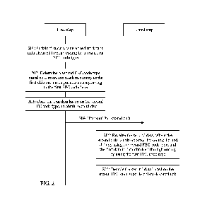
[0061] With reference to the implementation scenario shown in
FIG. 1, the data transmission
method provided in embodiments of this application is shown in FIG. 2, and
includes but is not
limited to step 201 to step 206.
[0062] Step 201: A first chip obtains first data, where the first data is
data obtained through
coding by using a first FEC code type.
[0063] In a possible implementation, the first data is data
inside the first chip, or the first data
is data that is received by the first chip and that is sent by a second chip.
For example, the first
chip codes original data by using the first FEC code type to obtain the first
data, or the second chip
codes original data by using the first FEC code type to obtain coded data. The
second chip
scrambles the coded data to form the first data, and the first chip receives
the first data sent by the
second chip. For example, the second chip sends the first data to the first
chip through a physical
channel. Regardless of whether the first data is the data inside the first
chip or the data sent by the
second chip, in addition to coding by using the first FEC, other processing
may be performed on
the first data. For example, the first data is data sent by the second chip to
the first chip by using a
physical medium attachment sublayer (physical medium attachment sublayer, PMA)
and/or a
physical medium dependent (physical media dependent, PMD) interface; or the
first data may be
data passing through the PMA and/or a physical coding sublayer (physical
coding sublayer, PCS)
in the first chip. In addition, the first data may alternatively be data on
which another processing
is performed. For example, the first data is data obtained after interleaving
and distributing are
performed.
[0064] The first FEC code type is not limited in this embodiment
of this application. In a
possible implementation, the first FEC code type is any one of a Reed-Solomon
(Reed-Solomon,
RS) code, a Bose-Chaudhuri-Hocquengliem (Bose-Chaudhuri-T-Tocquenghem, BCH)
code, a fire
(fire) code, a turbo (turbo) code, a turbo product code (turbo product code,
TPC), a staircase
(staircase) code, and a low-density parity-check (low-density parity-check,
LDPC) code.
CA 03206435 2023- 7- 25
[0065] In addition, after receiving the first data, the first
chip may directly transmit the first
data. To improve data transmission quality, the first data may alternatively
be re-coded. A
triggering manner of performing concatenated coding by the first chip is not
limited in this
embodiment of this application. In a possible implementation, the first chip
performs auto-
negotiation with a third chip that receives data sent by the first chip; and
in response to an auto-
negotiation result indicating that concatenated coding is required, the first
chip determines the
second FEC code type based on the reference clock frequency of the first chip
and the output rate
corresponding to the first FEC code type. The auto-negotiation process may be
performed after
the first data is received, or may be performed before the method is
performed. An occasion of
auto-negotiation is not limited in this embodiment of this application, and
auto-negotiation only
needs to be performed before the first data is transmitted.
[0066] Step 202: Determine the second FEC code type based on the
reference clock frequency
of the first chip and the output rate corresponding to the first FEC code
type.
100671 In a possible implementation, the reference clock
frequency of the first chip, the output
rate corresponding to the first FEC code type, a codeword length of the second
data, and an
information length in a codeword of the second data meet an overhead
proportional relationship.
Determining the second FEC code type based on the reference clock frequency of
the first chip
and the output rate corresponding to the first FEC code type includes:
determining the second FEC
code type based on the reference clock frequency of the first chip, the output
rate corresponding
to the first FEC code type, and the overhead proportional relationship. The
second FEC code type
is determined based on the overhead proportional relationship, so that
overheads obtained through
coding by using the second FEC code type can be ensured, and data transmission
performance is
further improved.
100681 In a possible implementation, the overhead proportional
relationship includes:
¨nXV, =pxf Formula (1)
100691 Here, n is the codeword length of the second data, k is
the information length in the
codeword of the second data, vi is the output rate corresponding to the first
FEC code type, p is an
adjustment parameter, f is the reference clock frequency of the first chip,
and p is a positive integer.
100701 It should be noted that there are different combinations
of n, k, and p, provided that the
foregoing overhead proportion relationship can be met. For example, the
adjustment parameter is
a reference value, for example, the adjustment parameter is an integer
multiple of 10 or an integer
II
CA 03206435 2023- 7- 25
multiple of 20. Based on the reference value, a second FEC code type that
meets the overhead
proportional relationship is determined.
[0071] For example, the first FEC code type is RS (544, 514),
the reference clock frequency
of the first chip is 156.25 megahertz (MHz), and the output rate corresponding
to the first FEC
code type is 106.25 gigabits per second (Gbps). For example, when p = 705, n =
282, and k = 272.
When p = 720, n = 144, k = 136, or n = 180, k = 170. For another example, if
the adjustment
parameter is 720, n = 144 and k = 136, or n = 180 and k = 170.
[0072] In a possible implementation, when the second FEC code
type is determined based on
the overhead proportional relationship, the second FEC code type may be
determined with
reference to Table 1, where all code types in Table 1 are BCH codes.
Table 1
Quantity of extended bits included in n
0 180 170 10
1
162 153 9
1
144 136 8
1
126 119 7
1
1 198 187 10
1
180 170 9
1
162 153 8
1
2 216 204 10
1
198 187 9
1
180 170 8
1
[0073] In Table 1, n is a codeword length, k is an information
length in a codeword, m indicates
that a finite field (finite field) or Galois field (Galois Field) in which the
code is located is GF (2'),
and t is an error correction capability. For example, BCH (180, 170, m = 10, t
= 1) indicates that a
codeword length of the BCH code type is 180 bits (bit), the length includes 0
extended bits
(extended bit), the information length in the codeword is 170 bits, m = 10,
and the error correction
capability is 1. eBal (161 + 1, 153, m= 8, t = 1) indicates that the BCH code
type is a BCH code
12
CA 03206435 2023- 7- 25
type including an extended bit, the codeword length is 162 bits, the length
includes one extended
bit, m = 8, and the error correction capability is 1. A principle of another
BCH code type in Table
1 is the same as that of the foregoing BCH code type. Details are not
described herein again.
[0074] In a possible implementation, the codeword length of the
second data is in an integer
multiple relationship with a quantity of logical channels through which the
second data is
distributed. The logical channel may be a PCS channel or an FEC channel. When
the second FEC
code type is determined, the integer multiple relationship is considered, so
that the determined
second FEC code type is more suitable for a transmission scenario, and data
transmission
performance is improved. For example, when the quantity of logical channels
through which the
second data is distributed is 8, the codeword length of the second data is an
integer multiple of 8.
Certainly, the quantity of logical channels may alternatively be 1, that is,
the second data is
transmitted through one logical channel. Because the codeword length of the
second data is a
positive integer, the codeword length of the second data is also in an integer
multiple relationship
with the quantity of logical channels through which the second data is
distributed.
[0075] A manner of determining the second FEC code type based on the
reference clock
frequency of the first chip and the output rate corresponding to the first FEC
code type includes
but is not limited to the following three manners.
[0076] Manner 1: The first chip first determines a first set
based on the reference clock
frequency of the first chip, the output rate corresponding to the first FEC
code type, and the
overhead proportional relationship, where the first set includes a plurality
of FEC code types that
meet the overhead proportional relationship. Then, the second FEC code type is
determined from
the first set based on an integer multiple relationship between the codeword
length and the logical
channel during distribution.
[0077] Manner 2: The first chip first determines a second set
based on an integer multiple
relationship between a codeword length and a logical channel during
distribution, where the
second set includes a plurality of FEC code types that meet the integer
multiple relationship. Then,
the second FEC code type is determined from the second set based on the
reference clock
frequency of the first chip and the output rate corresponding to the first FEC
code type based on
the overhead proportional relationship.
[0078] Manner 3: The first chip first determines a first set based on the
reference clock
frequency of the first chip, the output rate corresponding to the first FEC
code type, and the
13
CA 03206435 2023- 7- 25
overhead proportion relationship, where the first set includes a plurality of
FEC code types that
meet the overhead proportion relationship. Then, a second set is determined
based on an integer
multiple relationship between a codeword length and a logical channel during
distribution, where
the second set includes a plurality of FEC code types that meet the integer
multiple relationship,
and the second FEC code type is determined based on the first set and the
second set. For example,
the first chip determines the second FEC code type based on an intersection of
the first set and the
second set.
100791 It should be noted that the second FEC code type may be
any one of the RS code, the
BCH code, the fire code, the turbo code, the turbo product code, the staircase
code, or the LDPC
code. A type of the second FEC code type is not limited in this embodiment of
this application.
100801 Step 203: The first chip codes the first data based on
the second FEC code type, to
obtain the second data.
100811 In a possible implementation, if the first data is the
data inside the first chip, the first
chip codes the first data based on the second FEC code type, to obtain the
second data. If the first
data is the data that is received by the first chip and that is sent by the
second chip, the first chip
may directly code the data based on the second FEC code type, to obtain the
second data. It should
be noted that the first chip may perform a simple operation other than
decoding on the received
data, for example, bit multiplexing (bit mux) or bit demultiplexing (bit
demux).
100821 For example, if the first data is a single piece of data,
the first chip codes the first data
based on the second FEC code type, to obtain the second data, where the first
data may be data
directly received by the first chip, or data obtained by interleaving a
plurality of pieces of subdata
distributed by the first chip. In this case, the first data is considered as a
whole, and the first data
is coded by using the second FEC code type. Optionally, if there are a
plurality of pieces of first
data, for example, a plurality of pieces of first data sent by the second
chip, the first chip separately
codes each piece of first data based on the second FEC code type, to obtain a
plurality of pieces of
second data. As shown in FIG. 3, the first chip receives third data through an
attachment unit
interface (attachment unit interface, AUI), and processes the third data by
using a physical medium
attachment sublayer (physical medium attachment sublayer, PMA), to obtain a
plurality of pieces
of first data. The first chip separately codes the plurality of pieces of
first data, to obtain a plurality
of pieces of second data. The obtained plurality of pieces of second data may
be transmitted
through a plurality of physical channels (physical channels 1 to N in FIG. 5),
and then transmitted
14
CA 03206435 2023- 7- 25
outwards by using the PMA, a physical media dependent (physical media
dependent, PMD), or
the like. In some embodiments, in FIG. 3, the second chip may be a physical
layer (PHY) chip in
a network device, for example, a router or a switch, and the first chip may be
a chip in an optical
module, or a clock data recovery (clock data recovery, CDR)/retimer (retimer)
chip. The PRY chip
may be a chip located on a board of the network device. The chip may be a
central processing unit
(central processing unit, CPU), a network processor (network processor, NP), a
neural network
processing unit (neural network processing unit, NPU), a field programmable
gate array (field
programmable gate array, FPGA), a programmable logic controller (programmable
logic controller,
PLC), or the like, or any combination thereof
[0083] In a possible implementation, regardless of one piece of first data
or a plurality of pieces
of first data, that the first chip codes the first data based on the second
FEC code type, to obtain
second data includes: The first chip distributes the first data to obtain a
plurality of pieces of first
subdata, and the first chip separately codes the plurality of pieces of first
subdata based on the
second FEC code type to obtain a plurality of pieces of second subdata. For
example, the process
may be shown in FIG. 4.
[0084] For example, a manner in which the first chip distributes
the first data to obtain the
plurality of pieces of first subdata includes but is not limited to the
following two manners.
[0085] Manner 1: The first chip distributes the first data
through the logical channel to obtain
the plurality of pieces of first subdata.
[0086] For example, the first chip distributes the first data through N
logical channels to obtain
the plurality of pieces of first subdata, where each logical channel is used
to transmit one piece of
first subdata, and the logical channel may be the PCS channel or the FEC
channel. The first chip
separately codes the plurality of pieces of first subdata based on the second
FEC code type, to
obtain the plurality of pieces of second subdata. For example, the process may
be shown in FIG.
5. The obtained plurality of pieces of second subdata may be separately
transmitted to the outside
by using the PMA, the PMD, or the like.
[0087] Manner 2: The first chip distributes the first data
through the PMA to obtain the
plurality of pieces of first subdata.
[0088] Step 204: The first chip transmits the second data.
[0089] The first chip transmits the second data through the logical
channel, and the logical
channel may be the PCS channel or the FEC channel. in a possible
implementation, for a quantity
CA 03206435 2023- 7- 25
of data transmission channels, that the first chip transmits the second data
includes but is not
limited to the following two cases.
[0090] Case 1: A quantity of channels is 1.
[0091] In case 1, the first chip transmits the second data
through the channel, and the second
data may be a single piece of data, or include a plurality of pieces of second
subdata.
[0092] Case 2: A quantity of channels is a positive integer
greater than or equal to 2.
[0093] In case 2, the first chip distributes the second data to
obtain a plurality of pieces of third
subdata, and sends the plurality of pieces of third subdata through a
plurality of logical channels.
For example, the first chip distributes the second data in round-robin
distribution. For example, as
shown in FIG. 6, there are N logical channels, and N is a positive integer
greater than or equal to
2. The first chip distributes the second data in round-robin distribution to
obtain N pieces of third
subdata, and sends the N pieces of third subdata through the N logical
channels. For example, each
of the N logical channels correspondingly sends one piece of third subdata.
The N pieces of third
subdata include but are not limited to being sent to a next chip through the
PMA and the PMD.
[0094] For example, if the first data is a single piece of data, after
coding the single piece of
first data by using the second FEC code type to obtain the second data, the
first chip distributes
the second data to obtain a plurality of pieces of third subdata, and sends
the plurality of pieces of
third subdata through a plurality of logical channels. If the first data is
distributed as a plurality of
pieces of first subdata, any one of the plurality of pieces of first subdata
is coded by using the
second FEC code type to obtain the second subdata, the first chip distributes
the plurality of pieces
of second subdata to obtain a plurality of pieces of third subdata, and sends
the plurality of pieces
of third subdata through a plurality of logical channels. For example, the
first chip distributes any
one of the plurality of pieces of second subdata in round-robin distribution.
Taking the system
shown in FIG. 7 as an example, the plurality of pieces of second subdata are
obtained through
coding by using the second FEC code type. For each piece of second subdata,
the first chip
distributes the second subdata to obtain N pieces of third subdata, where N is
a positive integer
greater than or equal to 2, and the plurality of pieces of third subdata are
distributed through the N
logical channels. For example, each of the N logical channels correspondingly
sends one piece of
third subdata.
[0095] The foregoing step 201 to step 204 are all processes in which the
first chip side
performs data transmission. The following uses a third chip side as an example
to describe the data
16
CA 03206435 2023- 7- 25
transmission method.
[0096] Step 205: The third chip receives second data, where the
second data is the data
obtained by coding the first data by using the second FEC code type, and the
first data is the data
obtained through coding by using the first FEC code type.
[0097] In a possible implementation, the third chip receives, through the
logical channel, the
second data sent by the first chip.
[0098] Step 206: The third chip decodes the second data based on
the second FEC code type,
to obtain decoded data.
[0099] The second data is obtained by coding the first data by
using the second FEC code type,
and the first data is obtained through coding by using the first FEC code
type. Therefore, the second
data received by the third chip has a higher coding gain and a higher error
correction capability.
The obtained decoded data has higher accuracy by decoding the second data.
[00100] In a possible implementation, the third chip performs auto-negotiation
with the first
chip that sends the second data. In response to an auto-negotiation result
indicating that decoding
needs to be performed, the third chip decodes the second data based on the
second FEC code type,
to obtain the decoded data.
[00101] That the third chip decodes the second data based on the second FEC
code type includes
but is not limited to: The third chip performs soft-decision decoding on the
second data based on
the second FEC code type. For example, that the third chip performs soft-
decision decoding on the
second data based on the second FEC code type, to obtain the decoded data
includes: The third
chip obtains a first sequence of the second FEC code type based on the second
data, where the first
sequence includes a plurality of symbol elements. The third chip separately
allocates a reliability
metric to each of the plurality of symbol elements; the third chip determines
at least one most
unreliable location based on the reliability metric; and the third chip
obtains an error pattern based
on the at least one most unreliable location, and corrects the first sequence
based on the error
pattern. The third chip performs algebraic decoding on the corrected first
sequence to obtain a first
codeword set, maps codewords in the first codeword set, and the third chip
obtains the decoded
data based on a mapping result.
[00102] in a possible implementation, after the third chip decodes the second
data based on the
second EEC code type, to obtain the decoded data, the method further includes:
The third chip re-
codes the decoded data based on a third FEC code type, and transmits the re-
coded data. Data
17
CA 03206435 2023- 7- 25
transmission quality of a next link can be protected by re-coding the decoded
data based on the
third FEC code type. The third FEC code type is not limited in this embodiment
of this application.
For example, the third FEC code type is a second FEC code type, and the second
FEC code type
may be the same as the second FEC code type for coding the second data, or may
be another
second FEC code type that meets the foregoing overhead proportion relationship
and a relationship
in which a codeword length is an integer multiple of a quantity of logical
channels during
distribution.
[00103] For example, as shown in FIG. 8, after the third chip decodes the
second data based on
the second FEC code type to obtain the decoded data, the third chip needs to
transmit the decoded
data to a fourth chip, and the fourth chip may process the received data as a
processing manner of
the first chip. For example, the decoded data is re-coded according to the
foregoing processes of
step 202 to step 204, and the re-coded data is transmitted. Optionally, the
fourth chip may
alternatively decode the received data based on the first FEC code type, to
obtain service data.
[00104] According to the method provided in this embodiment of this
application, the second
FEC code type is determined based on the reference clock frequency ofthe first
chip and the output
rate corresponding to the first FEC code type, and the obtained first data
coded by using the first
FEC code type is re-coded by using the second FEC code type, to obtain the
second data in
concatenated coding. Therefore, the second data has a higher coding gain, and
when the data is
transmitted on a channel on which a bit error easily occurs, error correction
can be effectively
performed on data on which a bit error occurs, thereby improving data
transmission quality.
[00105] in addition, because the second data is data obtained by directly
coding on the basis of
the first data, an implementation process of the method is simple, and data
transmission efficiency
is improved.
[00106] In addition, in the method, chips perform auto-negotiation, and
perform, based on an
auto-negotiation result indicating that concatenated coding is required, a
process of determining
the second FEC code type based on the reference clock frequency of the first
chip and the output
rate corresponding to the first FEC code type, so that the chips can actively
determine whether
concatenated coding needs to be performed. This is more flexible for coding
data transmitted in
different channels.
[00107] An embodiment of this application further provides a data transmission
apparatus. FIG.
9 is a schematic diagram of a structure of a data transmission apparatus
according to an
18
CA 03206435 2023- 7- 25
embodiment of this application. Based on the following plurality of modules
shown in FIG. 9, the
data transmission apparatus shown in FIG. 9 can perform all or some operations
performed by a
first chip. It should be understood that the apparatus may include more
additional modules than
the shown modules or omit some of the shown modules. This is not limited in
embodiments of this
application. As shown in FIG. 9, the apparatus includes:
an obtaining module 901, configured to obtain first data, where the first data
is data
obtained through coding by using a first FEC code type;
a determining module 902, configured to determine a second FEC code type based
on
a reference clock frequency of the first chip and an output rate corresponding
to the first FEC code
type;
a coding module 903, configured to code the first data based on the second FEC
code
type, to obtain second data; and
a transmission module 904, configured to transmit the second data.
[00108] In a possible implementation, the reference clock frequency of the
first chip, the output
rate corresponding to the first FEC code type, a codeword length of the second
data, and an
information length in a codeword of the second data meet an overhead
proportional relationship.
The determining module 902 is configured to determine the second FEC code type
based on the
reference clock frequency of the first chip, the output rate corresponding to
the first FEC code type,
and the overhead proportional relationship.
[00109] In a possible implementation, the overhead proportional relationship
includes:
¨kxv1 =pxf
[00110] Herein, n is the codeword length of the second data, k is the
information length in the
codeword of the second data, vi is the output rate corresponding to the first
FEC code type, p is an
adjustment parameter, f is the reference clock frequency of the first chip,
and p is a positive integer.
1001111 In a possible implementation, the codeword length of the second data
is in an integer
multiple relationship with a quantity of logical channels through which the
second data is
distributed.
[00112] In a possible implementation, the coding module 903 is configured to:
distribute the
first data to obtain a plurality of pieces of first subdata, and separately
code the plurality of pieces
of first subdata based on the second FEC code type to obtain a plurality
ofpieces of second subdata.
The transmission module 904 is configured to transmit the plurality of pieces
of second subdata.
19
CA 03206435 2023- 7- 25
[00113] In a possible implementation, the coding module 903 is configured to
distribute the
first data through a PCS channel to obtain the plurality of pieces of first
subdata; or distribute the
first data stream through a PMA to obtain the plurality of pieces of first
subdata.
[00114] In a possible implementation, the transmission module 904 is
configured to: distribute
the second data to obtain a plurality of pieces of third subdata, and send the
plurality of pieces of
third subdata through a plurality of logical channels.
[00115] In a possible implementation, the apparatus further includes an auto-
negotiation
module, configured to perform auto-negotiation with a third chip that receives
data sent by the first
chip, where in response to an auto-negotiation result indicating that
concatenated coding is
required, the determining module 902 performs the step of determining a second
FEC code type
based on a reference clock frequency of the first chip and an output rate
corresponding to the first
FEC code type.
[00116] In a possible implementation, the first data is data
inside the first chip, or the first data
is data that is received by the first chip and that is sent by a second chip.
[00117] FIG. 10 is a schematic diagram of a structure of a data transmission
apparatus according
to an embodiment of this application. Based on the following plurality of
modules shown in FIG.
10, the data transmission apparatus shown in FIG. 10 can perform all or some
operations performed
by a third chip. It should be understood that the apparatus may include more
additional modules
than the shown modules or omit some of the shown modules. This is not limited
in embodiments
of this application. As shown in FIG. 10, the apparatus includes:
a receiving module 1001, configured to receive second data, where the second
data is
data obtained by coding first data by using a second FEC code type, and the
first data is data
obtained through coding by using a first FEC code type; and
a decoding module 1002, configured to decode the second data based on the
second
FEC code type, to obtain decoded data.
[00118] In a possible implementation, the decoding module 1002 is configured
to perform soft-
decision decoding on the second data based on the second FEC code type, to
obtain the decoded
data.
[00119] In a possible implementation, the apparatus further includes a coding
module,
configured to re-code the decoded data based on a third FEC code type; and a
transmission module,
configured to transmit the re-coded data.
CA 03206435 2023- 7- 25
1001201 In a possible implementation, the third FEC code type is the first FEC
code type or the
second FEC code type.
[00121] It should be understood that, when the apparatuses provided in FIG. 9
and FIG. 10
implement functions of the apparatuses, division into the foregoing functional
modules is only
used as an example for description. In actual application, the foregoing
functions may be allocated
to different functional modules for implementation based on a requirement. in
other words, an
inner structure of a device is divided into different functional modules, to
implement all or some
of the functions described above. In addition, the apparatuses provided in the
foregoing
embodiment and the method embodiments pertain to the same concept. For a
specific
implementation process of the apparatus, refer to the method embodiments.
Details are not
described herein again.
[00122] An embodiment of this application provides a data transmission device.
The device
includes a processor, where the processor is coupled to a memory, the memory
stores at least one
program instruction or code, and the at least one program instruction or code
is loaded and
executed by the processor, so that the data transmission device implements the
method in the
foregoing method embodiment.
[00123] Refer to FIG. 11. FIG. 11 is a schematic diagram of a structure of a
data transmission
device 1100 according to an example embodiment of this application. The data
transmission device
1100 is a transmit side/receive side device. The data transmission device 1100
shown in FIG. 11
is configured to perform operations related to the data transmission method
shown in FIG. 2. The
data transmission device 1100 is, for example, a network device such as a
switch or a router, and
another device (for example, a server or a PC) that includes a chip
concatenation mode. A hardware
structure of the data transmission device 1100 includes a communication
interface 1101 and a
processor 1102. Optionally, the communication interface 1101 and the processor
1102 are
connected through a bus 1104. The communication interface 1101 is configured
to obtain first data
and transmit second data. The processor may store instructions or program
code, and execute, by
invoking the instructions or the program code, a function performed by a first
chip or a function
performed by a third chip. Optionally, the network device further includes a
memory 1103. The
memory 1103 stores instructions or program code. The processor 1102 is
configured to invoke the
instructions or program code in the memory 1103, so that the network device
performs related
processing steps of the first chip in the foregoing method embodiment. In a
specific embodiment,
21
CA 03206435 2023- 7- 25
the data transmission device 1100 in this embodiment of this application may
include the first
chips in the foregoing method embodiments. The processor 1102 in the data
transmission device
1100 reads the instructions or program code in the memory 1103, so that the
data transmission
device 1100 shown in FIG. 11 can perform all or some operations performed by
the first chip.
[00124] In a specific embodiment, the data transmission device 1100 in this
embodiment of this
application includes the third chips in the foregoing method embodiments. The
processor 1102 in
the data transmission device 1100 reads the instructions or program code in
the memory 1103, so
that the data transmission device 1100 shown in FIG. 11 can perform all or
some operations
performed by the third chip.
[00125] For example, the processor 1102 is, for example, a general-purpose
central processing
unit (central processing unit, CPU), a digital signal processor (digital
signal processor, DSP), a
network processor (network processor, NP), a graphics processing unit
(graphics processing unit,
GPU), a neural-network processing unit (neural-network processing unit, NPU),
a data processing
unit (data processing unit, DPU), a microprocessor, or one or more integrated
circuits configured
to implement the solutions of this application. For example, the processor
1102 includes an
application-specific integrated circuit (application-specific integrated
circuit, ASIC), a
programmable logic device (programmable logic device, PLD) or another
programmable logic
device, a transistor logic device, a hardware component, or any combination
thereof. The PLD is,
for example, a complex programmable logic device (complex programmable logic
device, CPLD),
a field-programmable gate array (field-programmable gate array, FPCIA),
generic array logic
(generic array logic, GAL), or any combination thereof. The processor may
implement or execute
various logical blocks, modules, and circuits described with reference to
content disclosed in
embodiments of the present invention. Alternatively, the processor may be a
combination of
processors implementing a computing function, for example, including a
combination of one or
more microprocessors, or a combination of a DSP and a microprocessor.
[00126] Optionally, the data transmission device 1100 further
includes a bus. The bus is
configured to transfer information between components of the data transmission
device 1100. The
bus may be a peripheral component interconnect (peripheral component
interconnect, PCI for short)
bus, an extended industry standard architecture (extended industry standard
architecture, EISA for
short) bus, or the like. Buses may be classified into an address bus, a data
bus, a control bus, and
the like. For ease of representation, only one bold line is used to represent
the bus in FIG. 11, but
22
CA 03206435 2023- 7- 25
this does not mean that there is only one bus or only one type ofbus. In
addition to being connected
through a bus, the components of the data transmission device 1100 in FIG. 11
may be connected
in another manner. A connection manner of the components is not limited in
this embodiment of
the present invention.
[00127] For example, the memory 11 03 is a read-only memory (read-only memory,
ROM) or
another type of static storage device capable of storing static information
and instructions, or a
random access memory (random access memory, RAM) or another type of dynamic
storage device
capable of storing information and instructions, or is an electrically
erasable programmable read-
only memory (electrically erasable programmable read-only memory, EEPROM), a
compact disc
read-only memory (compact disc read-only memory, CD-ROM) or other compact disc
storage,
optical disc storage (including a compact disc, a laser disc, an optical disc,
a digital versatile disc,
a Blu-ray disc, and the like), a magnetic disk storage medium or another
magnetic storage device,
or any other medium capable of carrying or storing expected program code in an
instruction form
or a data structure form and capable of being accessed by a computer. However,
the memory is not
limited thereto. For example, the memory 1103 exists independently, and is
connected to the
processor 1102 through the bus. Alternatively, the memory 1103 may be
integrated into the
processor 1102.
[00128] The communication interface 1101 is any transceiver-type apparatus,
and is configured
to communicate with another device or a communication network. The
communication network
may be the Ethernet, a radio access network (RAN), a wireless local area
network (wireless local
area network, WLAN), or the like. The communication interface 1101 may include
a wired
communication interface, and may further include a wireless communication
interface.
Specifically, the communication interface 1101 may be an Ethernet (Ethernet)
interface, a fast
Ethernet (fast Ethernet, FE) interface, a gigabit Ethernet (gigabit Ethernet,
GE) interface, an
asynchronous transfer mode (asynchronous transfer mode, ATM) interface, a
wireless local area
network (wireless local area network, WLAN) interface, a cellular network
communication
interface, or a combination thereof The Ethernet interface may be an optical
interface, an electrical
interface, or a combination thereof In this embodiment of this application,
the communication
interface 1101 may be used by the data transmission device 1100 to communicate
with another
device.
[00129] in a specific implementation, in an embodiment, the processor 1102 may
include one
23
CA 03206435 2023- 7- 25
or more CPUs. Each of the processors may be a single-core (single-CPU)
processor, or may be a
multi-core (multi-CPU) processor. The processor herein may be one or more
devices, circuits,
and/or processing cores configured to process data (for example, computer
program instructions).
[00130] In a specific implementation, in an embodiment, the data transmission
device 1100 may
include a plurality of processors. Each of the processors may be a single-core
processor (single-
CPU) or a multi-core processor (multi-CPU). The processor herein may be one or
more devices,
circuits, and/or processing cores configured to process data (for example,
computer program
instructions).
[00131] In a specific implementation, in an embodiment, the data transmission
device 1100 may
alternatively include an output device and an input device. The output device
communicates with
the processor 1102, and may display information in a plurality of manners. For
example, the output
device may be a liquid crystal display (liquid crystal display, LCD), a light-
emitting diode (light-
emitting diode, LED) display device, a cathode ray tube (cathode ray tube,
CRT) display device,
or a projector (projector). The input device communicates with the processor
1102, and may
receive an input by a user in a plurality of manners. For example, the input
device may be a mouse,
a keyboard, a touchscreen device, or a sensing device.
[00132] In some embodiments, the memory 1103 is configured to store program
code for
performing the solutions of this application, and the processor 1102 may
execute the program code
stored in the memory 1103. In other words, the data transmission device 1100
may implement the
data transmission method provided in the method embodiment by using the
processor 1102 and
the program code in the memory 1103. The program code may include one or more
software
modules. Optionally, the processor 1102 may store program code or instructions
for performing
the solutions of this application.
[00133] In a specific embodiment, the data transmission device 1100 in this
embodiment of this
application may include the first chip in the foregoing method embodiments.
The processor 1102
in the data transmission device 1100 reads the program code in the memory 1103
or the program
code or instructions stored in the processor 1102, so that the data
transmission device 1100 shown
in FIG. 11 can perform all or some operations performed by the first chip.
[00134] In a specific embodiment, the data transmission device 1100 in this
embodiment of this
application includes the third chip in the foregoing method embodiments. The
processor 1102 in
the data transmission device 1100 reads the program code in the memory 1103 or
the program
24
CA 03206435 2023- 7- 25
code or instructions stored in the processor 1102, so that the data
transmission device 1100 shown
in FIG. 11 can perform all or some operations performed by the third chip.
[00135] The data transmission device 1100 may be further corresponding to the
apparatuses
shown in FIG. 9 and FIG. 10. Each functional module in the apparatuses shown
in FIG. 9 and FIG.
10 is implemented by using software of the data transmission device 1100. In
other words, the
functional modules included in the apparatuses shown in FIG. 9 and FIG. 10 are
generated after
the processor 1102 of the data transmission device 1100 reads the program code
stored in the
memory 1103.
[00136] The steps of the data transmission method shown in FIG. 2 are
completed by using an
integrated logic circuit of hardware in the processor of the data transmission
device 1100 or an
instruction in a form of software. The steps of the method disclosed with
reference to embodiments
of this application may be directly performed by a hardware processor, or may
be performed by
using a combination of hardware in the processor and a software module. The
software module
may be located in a mature storage medium in this field, such as a random
access memory, a flash
memory, a read-only memory, a programmable read-only memory, an electrically
erasable
programmable memory, or a register. The storage medium is located in the
memory, and the
processor reads information in the memory and performs the steps in the
foregoing method in
combination with the hardware in the processor. To avoid repetition, details
are not described
herein again.
[00137] An embodiment of this application further provides a data transmission
system. The
system includes a first data transmission device and a second data
transmission device. The first
data transmission device is configured to perform the method performed by the
first chip shown
in FIG. 2, and the second data transmission device is configured to perform
the method performed
by the third chip shown in FIG. 2.
[00138] For functions of the first data transmission device and the second
data transmission
device in the system, refer to related descriptions shown in FIG. 2. Details
are not described herein
again.
[00139] It should be understood that the processor may be a central processing
unit (central
processing unit, CPU), or may be another general-purpose processor, a digital
signal processor
(digital signal processor, DSP), an application-specific integrated circuit
(application-specific
integrated circuit, ASTC), a field-programmable gate array (field-programmable
gate array, FPGA)
CA 03206435 2023- 7- 25
or another programmable logic device, a discrete gate or a transistor logic
device, a discrete
hardware component, or the like. The general-purpose processor may be a
microprocessor or any
conventional processor. it is to be noted that the processor may be a
processor that supports an
advanced reduced instruction set computing machine (advanced RISC machine,
ARM)
architecture.
[00140] Further, in an optional embodiment, the memory may include a read-only
memory and
a random access memory, and provide instructions and data for the processor.
The memory may
further include a nonvolatile random access memory. For example, the memory
may further store
information of a device type.
[00141] The memory may be a volatile memory or a nonvolatile memory, or may
include both
a volatile memory and a nonvolatile memory. The nonvolatile memory may be a
read-only memory
(read-only memory, ROM), a programmable read-only memory (programmable ROM,
PROM),
an erasable programmable read-only memory (erasable PROM, EPROM), an
electrically erasable
programmable read-only memory (electrically EPROM, EEPROM), or a flash memory.
The
volatile memory may be a random access memory (random access memory, RAM),
used as an
external cache. By way of example but not limitation, many forms of RAMs may
be used, for
example, a static random access memory (static RAM, SRAM), a dynamic random
access memory
(dynamic random access memory, DRAM), a synchronous dynamic random access
memory
(synchronous DRAM, SDRAM), a double data rate synchronous dynamic random
access memory
(double data rate SDRAM, DDR SDRAM), an enhanced synchronous dynamic random
access
memory (enhanced SDRAM, ESDRAM), a synchlink dynamic random access memory
(synchlink
DRAM, SLDRAM), and a direct rambus random access memory (direct rambus RAM, DR
RAM).
[00142] A computer-readable storage medium is further provided. The storage
medium stores
at least one program instruction or code, and when the program instruction or
code is loaded and
executed by a processor, a computer is enabled to implement the data
transmission method shown
in FIG. 2.
[00143] This application provides a computer program. When the computer
program is
executed by a computer, a processor or the computer is enabled to perform
corresponding steps
and/or procedures in the foregoing method embodiments.
[00144] A chip is provided. The chip includes a processor, configured to:
invoke, from a
memory, instructions stored in the memory and run the instructions, so that a
device on which the
26
CA 03206435 2023- 7- 25
chip is installed performs the methods in the foregoing aspects.
[00145] Another chip is provided. The chip includes: an input interface, an
output interface, a
processor, and a memory. The input interface, the output interface, the
processor, and the memory
are connected to each other by using an internal connection path. The
processor is configured to
execute code in the memory. When the code is executed, the processor is
configured to perform
the methods in the foregoing aspects.
[00146] A device is provided, and includes the chip in any one of
the foregoing solutions.
[00147] A device is provided, and includes the first chip in any one of the
foregoing solutions
and/or the third chip in any one of the foregoing solutions.
[00148] In some embodiments, in FIG. 1 to FIG. 8, the second chip may be a
transmit side
device, for example, a physical layer (PHY) chip in a router, a switch, or a
server, and the first chip
may be an interface of the transmit side device, for example, a chip in an
optical module or a
CDR/retimer chip. The third chip may be an interface of a receive side device,
for example, a chip
in an optical module or a CDR/retimer chip, and the fourth chip may be a
physical layer (PHY)
chip in the receive side device. The PEW chip may be a chip located on a board
of a computing
device, and the chip may be a CPU, a network processor (network processor,
NP), a neural network
processing unit (neural network processing unit, NPU), a field programmable
gate array (field
programmable gate array, FPGA), a programmable logic controller (programmable
logic controller,
PLC), or the like, or any combination thereof.
[00149] In some embodiments, the first chip communicates with the second chip
by using an
AUT. in some embodiments, the third chip communicates with the fourth chip by
using an AUI.
[00150] in the foregoing embodiment, during soft decoding, first, calculating
confidence (also
referred to as reliability, reliability) of each bit in a received codeword
based on received quantized
soft-decision information, to obtain a confidence sequence; selecting M least
reliable bit locations
from the confidence sequence, and in the M least reliable bit locations, and
successively attempting
to perform bitwise inversion on all combinations of 0, 1, 2, ..., and N (N <
M) bit locations to
obtain a plurality of test codewords; and performing hard-decision decoding
error correction on
each test codeword; then calculating Euclidean distances between the
confidence sequence and all
corrected test codewords; and selecting a corrected test codeword
corresponding to a smallest
distance as a final corrected codeword output. If there is no correctable
codeword in the test
codewords, a hard-decision result corresponding to the original received
codeword is used as an
27
CA 03206435 2023- 7- 25
output codeword.
[00151] All or some of the foregoing embodiments may be implemented by using
software,
hardware, firmware, or any combination thereof. When software is used to
implement the
embodiments, all or a part of the embodiments may be implemented in a form of
a computer
program product. The computer program product includes one or more computer
instructions.
When the computer program instructions are loaded and executed on the
computer, the procedure
or functions according to this application are all or partially generated. The
computer may be a
general-purpose computer, a dedicated computer, a computer network, or other
programmable
apparatuses. The computer instructions may be stored in a computer-readable
storage medium, or
may be transmitted from a computer-readable storage medium to another computer-
readable
storage medium. For example, the computer instructions may be transmitted from
a website,
computer, server, or data center to another website, computer, server, or data
center in a wired (for
example, a coaxial cable, an optical fiber, or a digital subscriber line) or
wireless (for example,
infrared, radio, or microwave) manner. The computer-readable storage medium
may be any usable
medium accessible by the computer, or a data storage device, for example, a
server or a data center,
integrating one or more usable media. The usable medium may be a magnetic
medium (for
example, a floppy disk, a hard disk, or a magnetic tape), an optical medium
(for example, a DVD),
a semiconductor medium (for example, a solid-state drive, solid-state drive),
or the like.
[00152] hi the foregoing specific implementations, the objectives, technical
solutions, and
beneficial effects of this application are further described in detail. It
should be understood that the
foregoing descriptions are merely specific implementations of this
application, but are not intended
to limit the protection scope of this application. Any modification,
equivalent replacement,
improvement, or the like made based on the technical solutions of this
application shall fall within
the protection scope of this application.
[00153] A person of ordinary skill in the art may be aware that, with
reference to the
embodiments disclosed in this specification, the method steps and the modules
can be implemented
by using software, hardware, firmware, or any combination thereof. To clearly
describe the
interchangeability between the hardware and the software, the steps and
composition of each
embodiment have generally described above based on functions. Whether these
functions are
performed in a hardware or software manner depends on particular applications
and design
constraints of the technical solutions. A person of ordinary skill in the art
may use different
28
CA 03206435 2023- 7- 25
methods to implement the described functions for each particular application,
but it should not be
considered that the implementation goes beyond the scope of this application.
[00154] A person of ordinary skill in the art may understand that all or some
of the steps of
embodiments may be implemented by hardware or a program instructing related
hardware. The
program may be stored in a computer-readable storage medium. The storage
medium may include:
a read-only memory, a magnetic disk, or an optical disc.
[00155] When software is used to implement the embodiments, all or a part of
the embodiments
may be implemented in a form of a computer program product. The computer
program product
includes one or more computer program instructions. For example, the method in
embodiments of
this application may be described in a context of a machine-executable
instruction. The machine-
executable instruction is included in, for example, a program module executed
in a device on a
real or virtual processor of a target. Usually, the program module includes a
routine, a program, a
library, an object, a class, a component, a data structure, and the like, and
executes a specific task
or implements a specific abstract data structure. In various embodiments,
functions of program
modules may be combined or split between the described program modules. The
machine-
executable instruction for the program module may be executed locally or
within a distributed
device. In the distributed device, the program module may be located in both a
local storage
medium and a remote storage medium.
[00156] Computer program code used to implement the method in embodiments of
this
application may be written in one or more programming languages. The computer
program code
may be provided for a processor of a general-purpose computer, a dedicated
computer, or another
programmable data processing apparatus, so that when the program code is
executed by the
computer or the another programmable data processing apparatus,
functions/operations specified
in the flowcharts and/or block diagrams are implemented. The program code may
be executed all
on a computer, partially on a computer, as an independent software package,
partially on a
computer and partially on a remote computer, or all on a remote computer or
server.
[00157] In a context of embodiments of this application, the computer program
code or related
data may be carried by any appropriate carrier, so that a device, an
apparatus, or a processor can
perform various processing and operations described above. For example, the
carrier includes a
signal, a computer-readable medium, and the like.
[00158] For example, the signal may include propagating signals
in electrical, optical, radio,
29
CA 03206435 2023- 7- 25
sound, or other forms, such as carrier waves and infrared signals.
[00159] The machine-readable medium may be any tangible medium that includes
or stores a
program used for or related to an instruction execution system, apparatus, or
device. The machine-
readable medium may be a machine-readable signal medium or a machine-readable
storage
medium. The machine-readable medium may include but is not limited to an
electronic, magnetic,
optical, electromagnetic, infrared, or semiconductor system, apparatus, or
device, or any
appropriate combination thereof. More detailed examples of the machine-
readable storage medium
include an electrical connection with one or more wires, a portable computer
disk, a hard disk, a
random access memory (RAM), a read-only memory (ROM), an erasable programmable
read-
only memory (EPROM or flash memory), an optical storage device, a magnetic
storage device, or
any appropriate combination thereof.
[00160] It may be clearly understood by a person skilled in the art that, for
convenient and brief
description, for a detailed working process of the foregoing system, device,
and module, refer to a
corresponding process in the foregoing method embodiments. Details are not
described herein.
[00161] in the several embodiments provided in this application, it should be
understood that
the disclosed system, device, and method may be implemented in other manners.
For example, the
described device embodiment is merely an example. For example, the module
division is merely
logical function division and may be other division during actual
implementation. For example, a
plurality of modules or components may be combined or integrated into another
system, or some
features may be omitted or not performed. In addition, the displayed or
discussed mutual couplings
or direct couplings or communication connections may be implemented through
some interfaces,
and the indirect couplings or communication connections between the devices or
modules may be
electrical connections, mechanical connections, or connections in other forms.
[00162] The modules described as separate parts may or may not be physically
separate, and
parts displayed as modules may or may not be physical modules, may be located
in one position,
or may be distributed on a plurality of network modules. Some or all of the
modules may be
selected based on actual requirements to achieve the objectives of the
solutions in embodiments
of this application.
[00163] in addition, functional modules in embodiments of this application may
be integrated
into one processing module, or each of the modules may exist alone physically,
or two or more
modules may be integrated into one module. The integrated module may be
implemented in a form
CA 03206435 2023- 7- 25
of hardware, or may be implemented in a form of a software functional module.
[00164] When the integrated module is implemented in the form of a software
functional
module and sold or used as an independent product, the integrated module may
be stored in a
computer-readable storage medium. Based on such an understanding, the
technical solutions of
this application essentially, or the part contributing to the related art, or
all or some of the technical
solutions may be implemented in the form of a software product. The computer
software product
is stored in a storage medium and includes several instructions to cause a
computer device (which
may be a personal computer, a server, a network device, or the like) to
perform all or some of the
steps of the method in embodiments of this application. The foregoing storage
medium includes
any medium that can store program code, such as a USB flash drive, a removable
hard disk, a read-
only memory (read-only memory, ROM), a random access memory (random access
memory,
RAM), a magnetic disk, or an optical disc.
[00165] Ill this application, the terms "first", "second", and
the like are used to distinguish
between same or similar items whose effects and functions are basically the
same. It should be
understood that there is no logical or time-sequence dependency among "first",
"second", and "ntim,
and a quantity and an execution sequence are not limited. It should also be
understood that although
the terms such as "first" and "second" are used in the following description
to describe various
elements, these elements should not be limited by the terms. These terms are
merely used to
distinguish one element from another element. For example, without departing
from the scope of
various examples, a first network device may be referred to as a second
network device. Similarly,
a second network device may be referred to as a first network device. Both the
first network device
and the second network device may be network devices, and in some cases, may
be separate and
different network devices.
[00166] It should be further understood that sequence numbers of processes do
not mean
execution sequences in embodiments of this application. The execution
sequences of the processes
should be determined based on functions and internal logic of the processes,
and should not be
construed as any limitation on the implementation processes of embodiments of
this application.
[00167] In this application, the term "at least one" means one or more, and
the term "a plurality
of' means two or more. For example, a plurality of second packets mean two or
more second
packets. The terms "system" and "network" may be used interchangeably in this
specification.
[00168] It should be understood that the terms used in the descriptions of
various examples in
31
CA 03206435 2023- 7- 25
this specification are merely intended to describe specific examples, but are
not intended to
constitute a limitation. The tetuts "one" ("a" and "an") and "the" of singular
forms used in the
descriptions of various examples and the appended claims are also intended to
include plural forms,
unless otherwise specified in the context clearly.
[00169] it should be further understood that the term "include" (or
"includes", "including",
"comprises'', and/or "comprising"), when being used in this specification,
specifies the presence
of stated features, integers, steps, operations, elements, and/or components,
but does not preclude
the presence or addition of one or more other features, integers, steps,
operations, elements,
components, and/or groups thereof
[00170] It should be further understood that the term "if' may be interpreted
as a meaning
"when" ("when" or "upon"), "in response to determining", or "in response to
detecting". Similarly,
according to the context, the phrase "if it is determined that" or ''if (a
stated condition or event) is
detected" may be interpreted as a meaning of "when it is determined that" or
"in response to
determining" or "when (a stated condition or event) is detected" or "in
response to detecting (a
stated condition or event)".
[00171] It should be understood that determining B based on A does not mean
that B is
determined only based on A, but B may be determined based on A and/or other
information.
[00172] It should further be understood that "one embodiment", "an
embodiment", or "a
possible implementation" mentioned throughout this specification means that
particular features,
structures, or characteristics related to the embodiments or implementations
are included in at least
one embodiment of this application. Therefore, "in one embodiment", "in an
embodiment", or "in
a possible implementation" appearing throughout this specification does not
necessarily mean a
same embodiment. In addition, these particular features, structures, or
characteristics may be
combined in one or more embodiments by using any appropriate manner.
32
CA 03206435 2023- 7- 25