Note: Descriptions are shown in the official language in which they were submitted.
CA 03207089 2023-06-30
WO 2022/141331 PCT/CN2020/141894
1
METHOD AND APPARATUS FOR REDUCING PEAK TO AVERAGE POWER RATIO
rECHNICAL FIELD
The present disclosure relates to wireless communication systems and, more
specifically,
but not exclusively, to a system and method for reducing peak to average power
ratio (PAPR) in
a special field of a physical layer protocol data units (PPDUs).
BACKGROUND
A universal signal (U-SIG) field is used in 802.11be to convey information to
all
receivers about various important parameters such as a standard version
(802.11be or later
version), a bandwidth, number of extremely high throughput, EHT, signal (EHT-
SIG) symbols,
etc. The receivers include both access point (AP) and/or stations (STAs). The
U-SIG is
composed of 2 OFDM symbols, and each OFDM symbol contains 26 information bits.
Since 802.11be is divided into two releases ¨ Release 1 and Release 2, and
Release 2 is in
the progress of study, some bits within the U-SIG field are reserved.
There is an agreement to divide these reserved bits into two types:
- Validate bits ¨ used by the receiver to determine whether to continue
receiving the packet
or end the reception. For example, a Release 1 receiver may understand that
the packet is
intended for a Release 2 receiver so it can end the reception.
- Disregard bits ¨ bits that are defined as "don't care"
Both validate and disregard bits may be used for other purposes within Release
2.
At this stage in time, the disregard bits are all set to a value of '1' in a
multi-user (MU)
PPDU type (or 31 in decimal format). The disregard bits are copied from the
trigger-based (TB)
frame in a TB PPDU (validate bits are also set to '1').
The newly introduced disregard bits may cause some problems of performance for
both
MU PPDU and TB PPDU.
SUMMARY
It is an object of the present disclosure to provide a method and apparatus
for reducing
PAPR for transmitting a PPDU, thereby improving the transmitting performance
of the PPDU.
CA 03207089 2023-06-30
WO 2022/141331 PCT/CN2020/141894
2
The foregoing and other objects are achieved by the features of the
independent claims.
Further implementation forms are apparent from the dependent claims, the
description and the
figures.
According to a first aspect of the present disclosure, a communication device
is disclosed.
The communication device may be an AP or STA. The communication device is used
to transmit
a PPDU to one or more receiving devices and the PPDU comprises a universal
signal, U-SIG,
field, the communication device comprising a processor, configured to: operate
on a first
disregard bits sequence to obtain a second disregard bits sequence, wherein
the first disregard
bits sequence is with all bits set to '1'; and a transmitter, configured to:
transmit the PPDU,
wherein the PPDU comprises the second disregard bits sequence.
In a further implementation of the first aspect, the U-SIG comprises at least
a first U-SIG
symbol and a second U-SIG symbol.
In a further implementation of the first aspect, operation on a first
disregard bits sequence
to obtain a second disregard bits sequence comprises: set the value of the
first disregard bits
sequence to a sequence comprising at least one '0' bit; or change the value of
the validate bit
immediately after the first disregard bits sequence to '0' and modifying the
value of the first
disregard bits sequence to a pre-set value; or change the location of the
first disregard bits
sequence among U-SIG fields and change the value of the first disregard bits;
or replace a
portion of the first disregard bits sequence with a cyclic redundancy check,
CRC.
In a further implementation of the first aspect, setting the value of the
first disregard bits
sequence to a sequence comprising at least one '0' bit comprises: set the
first disregard bits
sequence of MU PPDU to one of the sequence in the set {`00101', '00110',
'01001', '01111',
'10011', '10101', '11000', '10110' } ; or set the first disregard bits
sequence of TB PPDU for the
first U-SIG symbol to one of the sequence in the set
{`010010','010011V010100', '010101',
'011100', '011101', '011110', '011111', '100101', '100010', '110100',
'111000', '111001'}; or
set the first disregard bits sequence of TB PPDU for the second U-SIG symbol
to one of the
sequence in the set {`01001', '01101', '01111', '11010', '11011', '11101',
'11110', '11111'}; or
set a single global value of the first disregard bits sequence within the
first U-SIG symbol for
different BW values for a TB PPDU, and the first disregard bits sequence is in
particularly set as
'011110' in binary; or set a single global value of the first disregard bits
in the second U-SIG
CA 03207089 2023-06-30
WO 2022/141331
PCT/CN2020/141894
3
symbol for different bandwidth values for a TB PPDU, and the first disregard
bits sequence is in
particularly set as '01001' or '11110' in binary.
In a further implementation of the first aspect, setting the value of the
first disregard bits
sequence to a sequence in the set of {`00101', '00110', '01001', '01111',
'10011', '10101',
'11000', '10110' } comprises: the first disregard bits sequence is set to
'00101' when the PPDU
is transmitted over 20MHz bandwidth; or the first disregard bits sequence is
set to one of
{`00101', '00110', '01001', '01111', '10011'} when the PPDU is transmitted
over 40MHz
bandwidth; or the first disregard bits sequence is set to one of {`00101',
'01111', '10011',
'11000' } when the PPDU is transmitted over 80MHz bandwidth; or the first
disregard bits
sequence is set to one of {`00101', '10101' } when the PPDU is transmitted
over 160MHz
bandwidth; or the first disregard bits sequence is set to one of {`00101',
'10110' } when the
PPDU is transmitted over 320MHz bandwidth; or the first disregard bits
sequence is set to
'00101' for any bandwidth.
In a further implementation of the first aspect, changing the value of the
validate bit
immediately after the first disregard bits sequence to '0' and modifying the
value of the first
disregard bits sequence to a pre-set value comprises: the pre-set value is set
to '01001' for
20MHz bandwidth.
In a further implementation of the first aspect, changing the location of the
first disregard
bits sequence among U-SIG fields and changing the value of the first disregard
comprises: move
the first disregard bits sequence after a basic service set, BSS, color field
and before a TXOP
field; or moving the first disregard bits sequence immediately before the BSS
color field.
In a further implementation of the first aspect, replacing a portion of the
first disregard
bits sequence with a cyclic redundant check, CRC, comprises: take one bit of
the first disregard
bits sequence as CRC indicator, wherein the CRC indicator indicates four CRC
bits are
comprised in the first disregard bits sequence.
In a further implementation of the first aspect, the four CRC bits are the
LSBs of an 8-bit
CRC, wherein the 8-bit CRC is computed over information bits transmitted over
the first U-SIG
symbol and the second U-SIG symbol.
In a further implementation of the first aspect, the 8-bit CRC is divided into
LSBs and
MSBs, wherein the MSBs are transmitted over the second U-SIG symbol.
In a further implementation of the first aspect, the indicator is set to '1'
or '0'.
CA 03207089 2023-06-30
WO 2022/141331 PCT/CN2020/141894
4
In a further implementation of the first aspect, the PPDU comprises: multi-
user, MU,
PPDU, or trigger-based, TB, PPDU.
According to a second aspect of the present disclosure, a method of reducing
peak to
average power ratio, PAPR, for transmitting a physical layer protocol data
unit, PPDU,
comprising: operating on a first disregard bits sequence to obtain a second
disregard bits
sequence, wherein the first disregard bits sequence is with all bits set to
'1'; and transmitting the
PPDU, wherein the PPDU comprises the second disregard bits sequence.
In a further implementation of the second aspect, the U-SIG comprises at least
a first U-
SIG symbol and a second U-SIG symbol.
In a further implementation of the second aspect, operating on a first
disregard bits
sequence to obtain a second disregard bits sequence comprises: set the value
of the first disregard
bits sequence to a sequence comprising at least one '0' bit; or change the
value of the validate
bit immediately after the first disregard bits sequence to '0' and modifying
the value of the first
disregard bits sequence to a pre-set value; or change the location of the
first disregard bits
sequence among U-SIG fields and change the value of the first disregard bits;
or replace a
portion of the first disregard bits sequence with a cyclic redundancy check,
CRC.
In a further implementation of the second aspect, setting the value of the
first disregard
bits sequence to a sequence comprising at least one '0' bit comprises: set the
first disregard bits
sequence of MU PPDU to one of the sequence in the set {`00101', '00110',
'01001', '01111',
'10011', '10101', '11000', '10110' } ; or set the first disregard bits
sequence of TB PPDU for the
first U-SIG symbol to one of the sequence in the set {`010010', '010011',
'010100', '010101',
'011100', '011101', '011110', '011111', '100101', '100010', '110100',
'111000', '111001'}; or
set the first disregard bits sequence of TB PPDU for the second U-SIG symbol
to one of the
sequence in the set {`01001', '01101', '01111', '11010', '11011', '11101',
'11110', '11111'}; or
set a single global value of the first disregard bits sequence within the
first U-SIG symbol for
different BW values for a TB PPDU, and the first disregard bits sequence is in
particularly set as
'011110' in binary; or set a single global value of the first disregard bits
in the second U-SIG
symbol for different bandwidth values for a TB PPDU, and the first disregard
bits sequence is in
particularly set as '01001' or '11110' in binary.
In a further implementation of the second aspect, setting the value of the
first disregard
bits sequence to a sequence in the set of {`00101', '00110', '01001', '01111',
'10011', '10101',
CA 03207089 2023-06-30
WO 2022/141331 PCT/CN2020/141894
'11000','10110'} comprises: the first disregard bits sequence is set to
'00101' when the PPDU is
transmitted over 20MHz bandwidth; or the first disregard bits sequence is set
to one of {`00101',
'00110', '01001', '01111', '10011' } when the PPDU is transmitted over 40MHz
bandwidth; or
the first disregard bits sequence is set to one of {`00101', '01111', '10011',
'11000'} when the
PPDU is transmitted over 80MHz bandwidth; or the first disregard bits sequence
is set to one of
{`00101', '10101' } when the PPDU is transmitted over 160MHz bandwidth; or the
first
disregard bits sequence is set to one of {`00101', '10110' } when the PPDU is
transmitted over
320MHz bandwidth; or the first disregard bits sequence is set to '00101' for
any bandwidth.
In a further implementation of the second aspect, changing the value of the
validate bit
immediately after the first disregard bits sequence to '0' and modifying the
value of the first
disregard bits sequence to a pre-set value comprises: the pre-set value is set
to '01001' for
20MHz bandwidth.
In a further implementation of the second aspect, changing the location of the
first
disregard bits sequence among U-SIG fields and changing the value of the first
disregard
comprises: move the first disregard bits sequence after a basic service set,
BSS, color field and
before a TXOP field; or moving the first disregard bits sequence immediately
before the BSS
color field.
In a further implementation of the second aspect, replacing a portion of the
first disregard
bits sequence with a cyclic redundant check, CRC, comprises: take one bit of
the first disregard
bits sequence as CRC indicator, wherein the CRC indicator indicates four CRC
bits are
comprised in the first disregard bits sequence.
In a further implementation of the second aspect, the four CRC bits are the
LSBs of a 8-
bit CRC, wherein the 8-bit CRC is computed over information bits transmitted
over the first U-
SIG symbol and the second U-SIG symbol.
In a further implementation of the second aspect, the 8-bit CRC is divided
into LSBs and
MSBs, wherein the MSBs are transmitted over the second U-SIG symbol.
In a further implementation of the second aspect, the indicator is set to '1'
or '0'.
In a further implementation of the second aspect, the PPDU comprises: multi-
user, MU,
PPDU, or trigger-based, TB, PPDU.
According to a third aspect of the present disclosure, a computer readable
storage
medium is provided. The computer readable storage medium stores an
instruction, and when the
CA 03207089 2023-06-30
WO 2022/141331 PCT/CN2020/141894
6
instruction runs on a computer, the computer is enabled to perform the method
of reducing
PAPR according to any one of the second aspect or the possible implementations
of the second
aspect.
According to a fourth aspect of the present disclosure, a computer program
product
including an instruction is provided. When the computer program product runs
on a computer,
the computer is enabled to perform the method of reducing PAPR according to
any one of the
second aspect or the possible implementations of the second aspect.
According to a fifth aspect of the present disclosure, a communications system
is
provided. The communications system includes a plurality of communication
devices, and the
plurality of communication devices include AP and STA, where the communication
device is
configured to support the method of reducing PAPR according to any one of the
second aspect or
the possible implementations of the second aspect.
According to a sixth aspect of the present disclosure, computer storage
medium, or
computer program product of any one of the methods of reducing PAPR is
configured to perform
the corresponding method provided above, and therefore, for beneficial effects
that the apparatus,
the computer storage medium, or the computer program product can achieve,
reference may be
made to beneficial effects of the corresponding method provided above. Details
are not described
herein again.
Other apparatus, methods, features, and advantages of the present disclosure
will be or
become apparent to one with skill in the art upon examination of the following
drawings and
detailed description. It is intended that all such additional apparatus,
methods, features, and
advantages be included within this description, be within the scope of the
present disclosure, and
be protected by the accompanying claims.
Unless otherwise defined, all technical and/or scientific terms used herein
have the same
meaning as commonly understood by one of ordinary skill in the art to which
embodiments.
Although methods and materials similar or equivalent to those described herein
can be used in
the practice or testing of embodiments, exemplary methods and/or materials are
described below.
In case of conflict, the patent specification, including definitions, will
control. In addition, the
materials, methods, and examples are illustrative only and are not intended to
be necessarily
limiting.
CA 03207089 2023-06-30
WO 2022/141331 PCT/CN2020/141894
7
BRIEF DESCRIPTION OF THE SEVERAL VIEWS OF THE DRAWINGS
Some embodiments are herein described, by way of example only, with reference
to the
accompanying drawings. With specific reference now to the drawings in detail,
it is stressed that
the particulars shown are by way of example and for purposes of illustrative
discussion of
embodiments. In this regard, the description taken with the drawings makes
apparent to those
skilled in the art how embodiments may be practiced.
FIG. 1 shows a system for reducing PAPR in a field of PPDUs according to some
embodiments of the present disclosure;
Fig. 2 shows a U-SIG design for an MU PPDU in 802.11be Release 1;
Fig. 3 shows a U-SIG design for a TB PPDU in 802.11be Release 1;
Fig. 4 shows a complimentary cumulative density function (CCDF) of the PAPR of
the
first U-SIG symbol for a 20MHz BW with an MU PPDU;
Fig. 5 shows a CCDF of the PAPR of the first U-SIG symbol for a 40MHz BW with
an
MU PPDU;
Fig. 6 is a schematic diagram of a possible logical structure of a
communication device in
the present disclosure according to some embodiments;
Fig. 7 shows the PAPR when the disregard bits sequence is set to '00101' for a
20MHz
MU PPDU;
Fig. 8 shows a PAPR CCDF of the first U-SIG symbol for 20MHz BW;
Fig. 9 shows a PAPR CCDF of the second U-SIG symbol with 20MHz BW;
Fig. 10 shows the PAPR of the first symbol for a 40MHz MU PPDU with the
disregard
bits sequence set to 5 in decimal;
Fig. 11 shows the PAPR of the second symbol for a 40MHz MU PPDU with the
disregard bits sequence set to one of 5, 6, 15 or 19 in decimal;
Fig. 12 shows a PAPR CCDF of the first U-SIG symbol for 40MHz BW with
disregard
bits sequence set to one of 19, 30, 31 or 52 in decimal for a TB PPDU;
CA 03207089 2023-06-30
WO 2022/141331 PCT/CN2020/141894
8
Fig. 13 shows a PAPR CCDF of the second U-SIG symbol for 40MHz BW with
disregard bit sequence set to one of 30, 39, 45 or 54 in decimal format;
Fig. 14 shows the PAPR for 80MHz MU PPDU of the first U-SIG symbol with
disregard
bits sequence set to one of 5, 15, or 24 in decimal;
Fig. 15 shows the PAPR for 80MHz MU PPDU of the second U-SIG symbol with
disregard bits sequence set to one of 5 or 19 in decimal;
Fig. 16 shows the PAPR for 80MHz TB PPDU of the first U-SIG symbol with
disregard
bits sequence set to one of 30, 44 or 56 in decimal;
Fig. 17 shows the PAPR of the second symbol for 80MHz TB PPDU with disregard
bits
sequence set to 30 in decimal in the first U-SIG symbol and set to one of 9,
26, 27, 30 or 31 in
decimal for the second U-SIG symbol;
Fig. 18 shows the PAPR of the second symbol for 160MHz MU PPDU with disregard
bits sequence set to 5 or 21 in decimal in the first U-SIG symbol;
Fig. 19 shows the PAPR of the first symbol for 160MHz TB PPDU with disregard
bits
sequence set to one of 30, 51 or 57 in decimal in the first U-SIG symbol;
Fig. 20 shows the PAPR of the first symbol for 320MHz MU PPDU with disregard
bits
sequence set to 5 or 22 in decimal in the first U-SIG symbol;
Fig. 21 shows the PAPR of the second symbol for 320MHz MU PPDU with disregard
bits sequence set to 5 or 19 or 21;
Fig. 22 shows the PAPR of the first U-SIG symbol for 320MHz TB PPDU with
disregard
bits sequence set to one of 18, 30, 31, 37 or 56 in decimal in the first U-SIG
symbol;
Fig. 23 shows the PAPR of the second U-SIG symbol for a 320MHz TB PPDU with
disregard bits sequence;
Fig. 24 shows the PAPR of the second symbol for 160MHz TB PPDU with disregard
bits
sequence set to 30 in decimal in the first U-SIG symbol and set to one of 9,
15, 29 or 30 in
decimal in the second U-SIG symbol;
Fig. 25 shows the CCDF for 20MHz MU PPDU with the validate bit set to '0' in
binary
and disregard bits sequence set to 9 in decimal;
CA 03207089 2023-06-30
WO 2022/141331 PCT/CN2020/141894
9
Fig. 26 shows the structure of the MU PPDU after relocating of the disregard
bits
sequence after BSS color field;
Fig. 27 shows the PAPR for a 20MHz MU PPDU of the first U-SIG symbols by
relocating the disregard bits sequence after BSS color field;
Fig. 28 shows the PAPR for a 20MHz MU PPDU of the second U-SIG symbols by
relocating the disregard bits sequence after BSS color field;
Fig. 29 shows the structure of the MU PPDU after relocating of the disregard
bits
sequence before BSS color field;
Fig. 30 shows the PAPR for a 20MHz MU PPDU of the first U-SIG symbols by
relocating the disregard bits sequence before BSS color field;
Fig. 31 shows the PAPR for a 20MHz MU PPDU of the second U-SIG symbols by
relocating the disregard bits sequence before BSS color field;
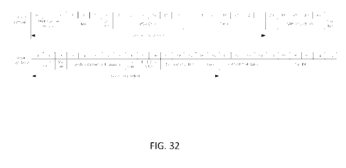
Fig. 32 shows the disregard bit sequence of the first U-SIG symbol is replaced
by an
indicator and 4 LSB CRC bits;
Fig. 33 shows the PAPR for a 20MHz MU PPDU of the first U-SIG symbols by
replacing the disregard bits sequence of the first U-SIG symbol with a 4 LSB
CRC bits and 1
indicator bit;
Fig. 34 shows the PAPR for a 20MHz MU PPDU of the second U-SIG symbols by
replacing the disregard bits sequence of the second U-SIG symbol with a 4 MSB
CRC bits.
DETAILED DESCRIPTION
Before explaining at least one embodiment in detail, it is to be understood
that
embodiments are not necessarily limited in its application to the details of
construction and the
arrangement of the components and/or methods set forth in the following
description and/or
illustrated in the drawings and/or the Examples. Implementations described
herein are capable of
other embodiments or of being practiced or carried out in various ways.
Fig. 1 shows a system for reducing PAPR in a field of PPDUs according to some
embodiments of the present disclosure. System 100, includes an access point
(AP) 101 and one
or more stations (STAs), for example STA 102, STA 103 and STA 104 shown in
Fig. 1. The
CA 03207089 2023-06-30
WO 2022/141331 PCT/CN2020/141894
system 100 is also called basic service set (BSS) in the present disclosure.
The AP 101 and/or
STAs in the system 100 are both called communication device. In some
embodiments, the
communication device may act as AP, while the communication device may act as
STA in some
other embodiments. In system 100, The AP and the STAs communicate in both
downlink and
uplink. The arrows between AP and STAs shown in Fig. 1 only show downlink, but
it should not
be understood as a limitation of transmission.
Although the system 100 shows only one AP in the system, the system may
include more
than one APs in the system and the APs in the system may perform coordination
transmission.
The system 100 in the present disclosure includes but is not limited to: a
wireless fidelity
(WIFI) communication system, a narrowband internet of things (NB-IoT) system,
a long term
evolution (LTE) system, a 5th generation mobile communications system (5G) or
beyond, a
machine to machine (M2M) communications system, or the like. The LTE system
and 5G or
beyond may integrate a WIFI system.
In the present disclosure, the communicate device may be AP 101 or STAs, and a
STA
may be for example, a mobile phone, an intelligent terminal, a tablet computer
(tablet), a
notebook computer (laptop), a video game console, a multimedia player, vehicle
which supports
WIFI, device to device (D2D) equipment, or any smart devices. The AP and/or
STA may be
stationary or mobile devices.
The WIFI system may support all the institute of electrical and electronic
engineers
(IEEE) 802.11 serials including but not limited to: 802.11a/b/g, 802.11n,
802.11ac, 802.11be,
802.11ax or beyond.
Fig. 2 shows a U-SIG design for an MU PPDU in 802.11be Release 1. The bits
contained
in a U-SIG' s first symbol of MU PPDU convey information about the physical
layer (PHY)
version (e.g. 802.11be or a later version of the standard), the bandwidth (BW)
(e.g. 20MHz,
40MHz etc.), whether it is a downlink (DL) or uplink (UL) transmission, the
BSS Color which is
used to differentiate between possibly different neighboring BSS values,
transmit opportunity
(TXOP) which may include duration of the TXOP and/or how long the transmitter
is taking
advantage of the channel resources.
CA 03207089 2023-06-30
WO 2022/141331 PCT/CN2020/141894
11
The bits contained in the U-SIG' s second symbol, for an MU PPDU, convey
information
about the PPDU type (e.g. MU PPDU, TB PPDU) and compression (e.g. non-OFDMA
PPDU
with reduced signaling), channel puncturing, the modulation and coding scheme
(MCS) which is
used for the EHT-SIG field and number of OFDM symbols used for the EHT-SIG
field, CRC
and 6 zero tail bits which is used for a convolutional code.
Fig. 3 shows a U-SIG design for a TB PPDU in 802.11be Release 1. The bits
contained in
the U-SIG' s first symbol of TB PPDU convey information about the PHY version
(e.g. 802.11be
or a later version of the standard), the BW (e.g. 20MHz, 40MHz etc.), whether
it is a DL or UL
transmission, the BSS Color which differentiates between possibly different
neighboring BSS
values, TXOP which may include duration of the TXOP and/or how long the
transmitter is
taking advantage of the channel resources. The bits contained in the U-SIG' s
second symbol, for
a TB PPDU, convey information about a PPDU type (e.g. MU, TB), spatial reuse
(e.g. spatial
reuse 1 and spatial reuse 2) which allows multiple transmitters to transmit
simultaneously on the
same resources, an MCS used for the EHT-SIG field and number of OFDM symbols
used for the
EHT-SIG field, a CRC and 6 zero tail bits used for the convolutional code.
As shown in both Fig. 2 and Fig. 3, the disregard bits are located in the
first U-SIG
symbol (also in the second U-SIG symbol for the TB PPDU); however, the CRC is
computed as
a function of all preceding bits which include both first U-SIG symbol and
second U-SIG symbol,
so the value of the CRC bits (located in the second U-SIG symbol) is a
function of the disregard
bits located in the first U-SIG symbol.
It should be noted that the disregard bits is also referred to as disregard
bits sequence in
some embodiments of the present disclosure. Disregard bits and disregard bits
sequence may be
used without differentiation in the present disclosure.
In current protocol, the disregard bits sequence is 5 bits and all bits are
set to '1' in an
MU PPDU type, or in other words, the disregard bits sequence in the MU PPDU is
set as 31 in
decimal format.
In 802.11ax, a trigger frame contains 9 reserved bits and all 9 bits are set
to '1'. The 9
reserved bits are copied to the second symbol of the HE-SIG-A field of a TB
PPDU. In the
current stage of 802.11be development, respective to a TB PPDU, there are 6
disregard bits in
the first U-SIG symbol and 5 disregard bits in the second U-SIG symbol. All
disregard bits are
CA 03207089 2023-06-30
WO 2022/141331 PCT/CN2020/141894
12
currently defined (in current stage of 802.11be development) as copied from
the trigger frame
(similar to 802.11ax operation). Maintaining the same design in llbe as it is
in 11 ax, the
disregard bits copied from the trigger frame will be set to one.
Although a structure of the trigger frame is not presented in the present
disclosure, the
disregard bits sequence in the trigger frame, MU PPDU and TB PPDU comprise
contiguous
binary bit '1' which can lead to high PAPR, and the performance of the U-SIG
field for an MU
PPDU and TB PPDU will be impacted in consequence (e.g. with lower PAPR, the
power
amplifier backoff can be reduced, thereby increasing efficiency).
Fig. 4 shows a complimentary cumulative density function (CCDF) of the PAPR of
the
first U-SIG symbol for a 20MHz BW for an MU PPDU. U-SIG-1 in Fig. 4 means the
first
symbol of the U-SIG field. With the design in the prior art, the PAPR of U-SIG
symbols is high
for all bandwidth scenarios. For example, in the 20MHz case, the CCDF of the
PAPR of the first
U-SIG symbol is compared with that of the data portion (assuming MCS 0 = BPSK
rate 1/2) and
with that of a legacy signal (L-SIG) field.
As shown in Fig. 4, the U-SIG-1 PAPR is higher on average than that of the
data for a
large proportion of the range. It is also not smooth (contains 'steps')
because of the large number
of fixed bits, which means the central limit theorem doesn't apply and hence
the distribution of
the time-domain signal isn't complex Gaussian.
Fig. 5 shows a CCDF of the PAPR of the first U-SIG symbol for a 40MHz BW. U-
SIG-1
in Fig. 5 means the first symbol of the U-SIG field. Current standard defines
that pre-EHT fields
that are duplicated on every 20MHz portion (e.g. L-SIG, U-SIG etc.) undergo
per-20MHz phase
rotation in order to reduce the PAPR. However, as shown in the Fig. 5 for the
first U-SIG symbol
in the 40MHz case, the U-SIG PAPR is higher than both data and L-SIG, which
means it is the
limiting factor in terms of performance (it may define the power amplifier
backoff).
It can be seen based on the simulation result from Fig. 4 and Fig. 5 that it
is therefore of
importance to reduce the PAPR of the U-SIG field.
In order to solve the problem above, the present disclosure provides a method
and/or
apparatus to reduce the PAPR of the trigger frame, MU PPDU and TB PPDU. The
present
disclosure provides a communication device comprising a processor, configured
to: operate on a
CA 03207089 2023-06-30
WO 2022/141331 PCT/CN2020/141894
13
first disregard bits sequence to obtain a second disregard bits sequence,
wherein the first
disregard bits sequence is with all bits set to '1'; and a transmitter
configured to: transmit the
PPDU, wherein the PPDU comprises the second disregard bits sequence. It should
be noted that,
the method and/or apparatus provided in the present disclosure may not
restrict it being used for
any other PPDUs or frames which have the same problem.
Embodiments present in the present disclosure may be a system, a method,
and/or a
computer program product. The computer program product may include a computer
readable
storage medium (or media) having computer readable program instructions
thereon for causing a
processor to carry out aspects of the embodiments.
The computer readable storage medium can be a tangible device that can retain
and store
instructions for use by an instruction execution device. The computer readable
storage medium
may be, for example, but is not limited to: an electronic storage device, a
magnetic storage
device, an optical storage device, an electromagnetic storage device, a
semiconductor storage
device, or any suitable combination of the foregoing.
A non-exhaustive list of more specific examples of the computer readable
storage
medium includes: a portable computer diskette, a hard disk, a random access
memory (RANI), a
read-only memory (ROM), an erasable programmable read-only memory (EPROM or
Flash
memory), a static random access memory (SRAM), a portable compact disc read-
only memory
(CD-ROM), a digital versatile disk (DVD), a memory stick, a floppy disk, and
any suitable
combination of the foregoing.
A computer readable storage medium, as used herein, is not to be construed as
being
transitory signals per se, such as radio waves or other freely propagating
electromagnetic waves,
electromagnetic waves propagating through a waveguide or other transmission
media (e.g., light
pulses passing through a fiber-optic cable), or electrical signals transmitted
through a wire.
Computer readable program instructions described herein can be downloaded to
respective computing/processing devices from a computer readable storage
medium or to an
external computer or external storage device via a network, for example, the
Internet, a local area
network, a wide area network and/or a wireless network. A network adapter card
or network
interface in each computing/processing device may receive computer readable
program
instructions from the network and forwards the computer readable program
instructions for
CA 03207089 2023-06-30
WO 2022/141331 PCT/CN2020/141894
14
storage in a computer readable storage medium within the respective
computing/processing
device.
Computer readable program instructions for carrying out operations of
embodiments may
be assembler instructions, instruction-set-architecture (ISA) instructions,
machine instructions,
machine dependent instructions, microcode, firmware instructions, state-
setting data, or either
source code or object code written in any combination of one or more
programming languages,
including an object oriented programming language such as Smalltalk, C++ or
the like, and
conventional procedural programming languages, such as the "C" programming
language or
similar programming languages.
The computer readable program instructions may execute entirely on the user's
computer,
partly on the user's computer, as a stand-alone software package, partly on
the user's computer
and partly on a remote computer or entirely on the remote computer or server.
In the latter
scenario, the remote computer may be connected to the user's computer through
any type of
network, including a local area network (LAN) or a wide area network (WAN), or
the
connection may be made to an external computer (for example, through the
Internet using an
Internet Service Provider).
In some embodiments, electronic circuitry including, for example, programmable
logic
circuitry, field-programmable gate arrays (FPGA), or programmable logic arrays
(PLA) may
execute the computer readable program instructions by utilizing state
information of the
computer readable program instructions to personalize the electronic
circuitry, in order to
perform aspects of embodiments.
Fig. 6 is a schematic diagram of a possible logical structure of a
communication device in
the present disclosure according to some embodiments. The communication device
includes a
processor 602. In some embodiments of the present disclosure, the processor
602 may be
configured to control and manage one or more actions of the communication
device, e.g.
configured to execute a code for operating on a first disregard bits sequence
to reduce the PAPR
and/or to process the data transmitted and/or received in the AP. Optionally,
the communication
device may further include a memory 601 and a communications interface 603.
The processor
602, the communications interface 603, and the memory 601 may be connected to
each other or
may be connected to each other by using a bus 604. The communications
interface 603 is
CA 03207089 2023-06-30
WO 2022/141331 PCT/CN2020/141894
configured to support the communication device in performing communication,
and the memory
601 is configured to store program code and data of the communication device.
The processor
602 calls the code stored in the memory 601 to perform control and management.
The memory
601 may or may not be coupled to the processor 602.
The processor 602 may be a central processing unit, a general-purpose
processor, a
digital signal processor, an application-specific integrated circuit, a field
programmable gate
array or another programmable logical device, a transistor logical device, a
hardware component,
or any combination thereof. The processor 602 may implement or execute various
example
logical blocks, modules, and circuits described with reference to content
disclosed in the present
disclosure. Alternatively, the processor 602 may be a combination of
processors implementing a
computing function, for example, a combination of one or more microprocessors,
or a
combination of the digital signal processor and a microprocessor. The bus 604
may be a
peripheral component interconnect (Peripheral Component Interconnect, PCI)
bus, an extended
industry standard architecture (Extended Industry Standard Architecture, EISA)
bus, or the like.
The bus may be classified into an address bus, a data bus, a control bus, and
the like.
According to the communication device provided above, in some embodiments, the
U-
SIG may comprise at least a first U-SIG symbol and a second U-SIG symbol.
In some embodiments, wherein operate on a first disregard bits sequence to
obtain a
second disregard bits sequence may comprise: set the value of the first
disregard bits sequence to
a sequence comprising at least one '0' bit; or change the value of the
validate bit immediately
after the first disregard bits sequence to '0' and modifying the value of the
first disregard bits
sequence to a pre-set value; or change the location of the first disregard
bits sequence among U-
SIG fields and change the value of the first disregard bits; or replace a
portion of the first
disregard bits sequence with a cyclic redundancy check, CRC.
The first disregard bits sequence in the present disclosure may be the
predefined bits
sequence in a prior art, e.g. present IEEE protocol. The first disregard bits
sequence in some
embodiments may be 5 or 6 bits and all bits are set as binary '1', e.g. in the
MU PPDU or TB
PPDU. The first disregard bits sequence may refer to the 6-bit disregard bits
of the first U-SIG
symbol in the TB PPDU, and/or to the 5-bit disregard bits of the second U-SIG
symbol in the TB
CA 03207089 2023-06-30
WO 2022/141331 PCT/CN2020/141894
16
PPDU. It should be noted that the disregard bits sequence may include other
number of binary
bits and 5-bit or 6-bit is not a limitation in the present disclosure.
In one embodiment, the value of the first disregard bits sequence is set to a
sequence
comprising at least one '0' bit in binary. Optionally, the first disregard
bits sequence may further
comprise at least one '1' bit in binary. The at least one '0' bit in binary
may be any bit of the
disregard bits sequence.
The first disregard bits sequence is set to a sequence comprising at least one
'0' bit in
binary may comprise the first disregard bits sequence of MU PPDU is set to for
example one of
the sequence in the binary set {`00101', '00110', '01001', '01111', '10011',
'10101', '11000',
'10110' } ; or the first disregard bits sequence of TB PPDU for the first U-
SIG symbol is set to
one of the sequence in the set {`010010', '010011', '010100', '010101',
'011100', '011101',
'011110', '011111', '100101', '100010', '110100', '111000', '111001'}; or the
first disregard
bits sequence of TB PPDU for the second U-SIG symbol is set to one of the
sequence in the set
{`01001', '01101', '01111', '11010', '11011', '11101', '11110', '11111'}; or
seta single global
value of the first disregard bits sequence within the first U-SIG symbol for
different BW values
for a TB PPDU, and the first disregard bits sequence is in particularly set as
'011110' in binary;
or set a single global value of the first disregard bits in the second U-SIG
symbol for different
bandwidth values for a TB PPDU, and the first disregard bits sequence is in
particularly set as
'01001' or '11110' in binary.
If the first disregard bits sequence of TB PPDU for the first U-SIG symbol is
set to one of
the sequence in the set {`010010', '010011', '010100', '010101', '011100',
'011101', '011110',
'011111', '100101', '100010', '110100', '111000', '111001'}, the first
disregard bits sequence
of TB PPDU for the second U-SIG symbol may be copied from trigger frame. It
should be
understood that the first disregard bits sequence of TB PPDU for the second U-
SIG symbol may
be set to any other value in the set for example {`01001', '01101', '01111',
'11010', '11011',
'11101', '11110', '11111' } . The value of the first disregard bits sequence
of TB PPDU for the
second U-SIG symbol is not restricted in this case.
If the first disregard bits sequence of TB PPDU for the second U-SIG symbol is
set to
one of the sequence in the set {`01001', '01101', '01111', '11010', '11011',
'11101', '11110',
'11111' }, the first disregard bits sequence of TB PPDU for the first U-SIG
symbol may be set
for example '011110' in binary (30 in decimal). It should be understood that,
the first disregard
CA 03207089 2023-06-30
WO 2022/141331 PCT/CN2020/141894
17
bits sequence of TB PPDU for the first U-SIG symbol may be set to any other
value in the set
{`010010', '010011', '010100', '010101', '011100', '011101', '011110',
'011111', '100101',
'100010%110100%111000%111001T
In one embodiment, for a 20MHz MU PPDU, the disregard bits sequence may be set
to
for example '00101' (5 in decimal format). For a disregard bits sequence of a
first symbol of a
TB PPDU, it may comprise 6 bits, and the MSB bit or LSB bit may be set to '0'
or '1' in binary,
which depends on the definition of standard.
Fig. 7 shows the PAPR when the disregard bits sequence is set to '00101' for a
20MHz
MU PPDU. It can be seen that the PAPR is greatly improved when the disregard
bits sequence
comprises at least one binary '0'.
In one embodiment, for a TB PPDU with 20MHz BW, replacing the 6 disregard bits
sequence in the first U-SIG symbol with one of {`010100', '011101', '011110',
'011111'} in
binary (20, 29, 30 and 31 in decimal respectively), and copying the 5
disregard bits in the 2nd U-
SIG symbol from the Trigger. It should be noted that the set {`010100',
'011101', '011110',
'011111'} in binary is subset of {`010010', '010011', '010100', '010101',
'011100', '011101',
'011110', '011111', '100101', '100010', '110100', '111000', '111001T
The choice of disregard bits sequence with 31 or 30 in decimal in the first U-
SIG symbol
leads to lower PAPR also in the second U-SIG symbol.
Fig. 8 shows a PAPR CCDF of the first U-SIG symbol for 20MHz BW. The disregard
bits in the second U-SIG symbol are assumed to be all ones (e.g. '11111').
In one embodiment, for a TB PPDU with 20MHz BW, replacing the 6 disregard bits
in
the first U-SIG symbol with '011110' in binary (30 in decimal format), and
replacing the 5
Disregard bits in the second U-SIG symbol with one of the set {`01001',
'11010', '11011',
'11110'} (9, 26, 27 and 30 respectively in decimal format).
Fig. 9 shows a PAPR CCDF of the second U-SIG symbol with 20MHz BW.
In one embodiment, for a 40MHz MU PPDU, the disregard bits sequence of the
first
symbol may be set to for example '00101' in binary (5 in decimal format) or
'01001' in binary (9
in decimal format).
CA 03207089 2023-06-30
WO 2022/141331 PCT/CN2020/141894
18
Fig. 10 shows the PAPR of the first symbol for a 40MHz MU PPDU with the
disregard
bits sequence set to 5 in decimal. It can be seen that the PAPR of first
symbol can be improved
with the disregard bits sequence of the present embodiment.
The disregard bits sequence of the MU PPDU may be set to for example one of
the set
{`00101', '00110', '01111', '10011' } in binary (5, 6, 15 and 19 respectively
in decimal format),
and the PAPR of the second U-SIG symbol can be improved in consequence.
Fig. 11 shows the PAPR of the second symbol for a 40MHz MU PPDU with the
disregard bits sequence set to one of 5, 6, 15 or 19 in decimal. It can be
seen that the PAPR is
greatly improved when the disregard bits sequence is set to one of {`00101',
'00110', '01111',
'10011'} in binary.
In one embodiment, for a TB PPDU with 40MHz BW, replacing the 6-bit disregard
bits
sequence in the first U-SIG symbol with {`010011', '011110', '011111',
'110100'} (19, 30, 31
and 52 respectively in decimal format), and the 5-bit disregard bits sequence
in the second U-
SIG symbol may be copied from a trigger frame. Fig. 12 shows a PAPR CCDF of
the first U-SIG
symbol for 40MHz BW with disregard bits sequence set to one of 19, 30, 31 or
52 in decimal for
a TB PPDU. The PAPR of the first symbol for 40MHz BW can then be improved. It
should be
noted that the set {`010100', '011101', '011110', '011111'} in binary is
subset of {`010010',
'010011', '010100', '010101', '011100', '011101', '011110', '011111',
'100101', '100010',
'110100%111000%111001T
Fig. 13 shows a PAPR CCDF of the second U-SIG symbol for 40MHz BW with
disregard bit sequence set to one of 30, 39, 45 or 54 in decimal format. It
can be seen that a
choice of disregard bit sequence set to 30 in decimal in the first U-SIG
symbol leads to lower
PAPR also in the second U-SIG symbol. Other values for reducing the second U-
SIG symbol's
PAPR are also marked.
In one embodiment, for the 80MHz MU PPDU considering the first U-SIG symbol,
the
disregard bits sequence may be set to one of {`00101', '01111', '11000'} in
binary (5, 15 and 24
respectively in decimal format).
CA 03207089 2023-06-30
WO 2022/141331 PCT/CN2020/141894
19
Fig. 14 shows the PAPR for 80MHz MU PPDU of the first U-SIG symbol with
disregard
bits sequence set to one of 5, 15, or 24 in decimal. It can be seen that the
PAPR of the first U-
SIG symbol be improved with the disregard bits sequence set to one of 5, 15,
or 24 in decimal.
In one embodiment, for the 80MHz MU PPDU considering the second U-SIG symbol,
the disregard bits sequence may be set to '00101', '10011' } in binary (5 and
19 respectively in
decimal format).
Fig. 15 shows the PAPR for 80MHz MU PPDU of the second U-SIG symbol with
disregard bits sequence set to one of 5 or 19 in decimal. It can be seen that
the PAPR of the
second U-SIG symbol can be improved with the disregard bits sequence set to 5
or 19 in decimal.
In order to improve the PAPR of both the first and the second U-SIG symbol, an
optimal
disregard bits sequence may be set to '00101' in binary for a 80MHz MU PPDU.
In one embodiment, for a TB PPDU with 80MHz BW, replacing the 6-bit disregard
bits
sequence in the first U-SIG symbol with {`011100', '011111', '100010',
'111000'} in binary (28,
31, 34 and 56 respectively in decimal), and the 5-bit disregard bits sequence
in the second U-SIG
symbol may be copied from the trigger frame. It should be noted that the set
{`010100',
'011101', '011110', '011111'} in binary is subset of {`010010', '010011',
'010100', '010101',
'011100', '011101', '011110', '011111', '100101', '100010', '110100',
'111000', '111001T
Fig. 16 shows the PAPR for 80MHz TB PPDU of the first U-SIG symbol with
disregard
bits sequence set to one of 30, 44 or 56 in decimal. The PAPR of the first U-
SIG symbol can be
improved with the disregard bits sequence set to one of 30, 44 or 56 in
decimal. The disregard
bits sequence in the second U-SIG symbol are all '1' in binary.
In one embodiment, for a TB PPDU with 80MHz BW, replacing the 6-bit disregard
bits
sequence in the first U-SIG symbol with '011110' in binary (30 in decimal
format), and
replacing the 5-bit disregard bits sequence in the second U-SIG symbol with
one of {`001001',
'011010', '011011', '011110', '011111'} in binary (9, 26, 27, 30 and 31
respectively in decimal).
Fig. 17 shows the PAPR of the second symbol for 80MHz TB PPDU with disregard
bits
sequence set to 30 in decimal in the first U-SIG symbol and set to one of 9,
26, 27, 30 or 31 in
decimal for the second U-SIG symbol. It can be seen that the PAPR can be
improved with the
CA 03207089 2023-06-30
WO 2022/141331 PCT/CN2020/141894
disregard bits sequence set to 30 in decimal in the first U-SIG symbol and set
to one of 9, 26, 27,
or 31 in decimal for the second U-SIG symbol.
In one embodiment, for a 160MHz MU PPDU, the disregard bits sequence may be
set to
one of {`00101', '10101'} in binary (5 and 21 respectively in decimal format).
Fig. 18 shows the
PAPR of the second symbol for 160MHz MU PPDU with disregard bits sequence set
to 5 or 21
in decimal in the first U-SIG symbol. The value 21 in decimal yields best
improvement for the
second U-SIG symbol and the value 5 in decimal yields a similar (almost as
good) improvement.
In one embodiment, for a TB PPDU with 160MHz BW, replacing the 6-bit disregard
bits
sequence in the first U-SIG symbol with {`011110', '110011', '111001'} in
binary (30, 51 and
57 respectively in decimal), and the 5-bit disregard bits in the second U-SIG
symbol may be
copied from the trigger frame. It should be noted that the set {`010100',
'011101', '011110',
'011111'} in binary is subset of {`010010', '010011', '010100', '010101',
'011100', '011101',
'011110', '011111', '100101', '100010', '110100', '111000', '111001T
Fig. 19 shows the PAPR of the first symbol for 160MHz TB PPDU with disregard
bits
sequence set to one of 30, 51 or 57 in decimal in the first U-SIG symbol. The
PAPR for the first
U-SIG symbol can be then improved. The disregard bits in the second U-SIG
symbol are
assumed to be set all '1' in binary.
In one embodiment, for a TB PPDU with 160MHz BW, replacing the 6-bit disregard
bits
sequence in the first U-SIG symbol with '011110' in binary (30 in decimal
format), and
replacing the 5-bit disregard bits sequence in the second U-SIG symbol with
one of {`01001',
'01111', '11101', '11110'} (9, 15,29 and 30 respectively in decimal).
In one embodiment, for a 320MHz MU PPDU, the disregard bits sequence may be
set to
one of {`00101', '10110'} in binary (Sand 22 respectively in decimal format).
Fig. 20 shows the
PAPR of the first symbol for 320MHz MU PPDU with disregard bits sequence set
to 5 or 22 in
decimal in the first U-SIG symbol. Fig. 21 shows the PAPR of the second symbol
for 320MHz
MU PPDU with disregard bits sequence set to 5 or 19 or 21. The value 19 in
decimal yields the
best improvement for the second U-SIG symbol and the value 5 in decimal yields
a similar
(almost as good) improvement.
CA 03207089 2023-06-30
WO 2022/141331 PCT/CN2020/141894
21
In one embodiment, for a TB PPDU with 320MHz BW, replacing the 6-bit disregard
bits
sequence in the first U-SIG symbol with f'010010', '011110',
'011111','100101','111000' f in
binary (18, 30, 31, 37, 56 respectively in decimal), and the 5-bit disregard
bits in the second U-
SIG symbol may be copied from the trigger frame. It should be noted that the
set {'010010',
'011110', '0111111100101V111000'} in binary is subset of f'010010', '010011',
'010100',
'010101', '011100', '011101', '011110', '011111', '100101', '100010',
'110100', '111000',
'111001' f.
Fig. 22 shows the PAPR of the first U-SIG symbol for 320MHz TB PPDU with
disregard
bits sequence set to one of 18, 30, 31, 37 or 56 in decimal in the first U-SIG
symbol. The PAPR
for the first U-SIG symbol can then be improved. The disregard bits in the
second U-SIG symbol
are assumed to be set all '1' in binary.
In one embodiment, for a TB PPDU with 320MHz BW, replacing the 6-bit disregard
bits
sequence in the first U-SIG symbol with '011110' in binary (30 in decimal
format), and
replacing the 5-bit disregard bits sequence in the second U-SIG symbol with
one of f'01001',
'01101', '11110'} (9, 13 and 30 respectively in decimal). Fig. 23 shows the
PAPR of the second
U-SIG symbol for a 320MHz TB PPDU with disregard bits sequence, in the second
U-SIG
symbol, set to one of 9, 13 or 30, when the disregard bits sequence in the
first U-SIG symbol is
set to 30 (in decimal format). The PAPR for the second U-SIG symbol can then
be improved.
In one embodiment, using a single global value of the disregard bits within
the first U-
SIG symbol to reduce the PAPR for all BW values for a TB PPDU. For example,
looking at the
results from the previous embodiments, by replacing the first disregard bits
sequence with 30 in
decimal, the PAPR for all BW values can get an improvement.
In one embodiment, using a single global value of the disregard bits within
the second U-
SIG symbol to reduce the PAPR for all BW values for a TB PPDU. For example,
looking at the
results from the previous Section, by replacing the first disregard bits
sequence with 9 or 30 in
decimal. The PAPR for all BW values can get an improvement.
Fig. 24 shows the PAPR of the second symbol for 160MHz TB PPDU with disregard
bits
sequence set to 30 in decimal in the first U-SIG symbol and set to one of 9,
15, 29 or 30 in
decimal in the second U-SIG symbol. The PAPR for the second U-SIG symbol can
then be
improved.
CA 03207089 2023-06-30
WO 2022/141331 PCT/CN2020/141894
22
In one embodiment, using a single global value of the Disregard bits to reduce
the PAPR
for all BW values for an MU PPDU. For example, looking at the results from the
previous
embodiments, by using disregard bits sequence '00101' in decimal (5 in
decimal) we can get an
improvement in PAPR for all BW values.
In one embodiment, operation on a first disregard bits sequence may include
change the
value of the validate bit immediately after the first disregard bits sequence
to '0' and modifying
the value of the first disregard bits sequence to a pre-set value. For
example, in the 20MHz MU
PPDU using disregard bits sequence of '01001' in binary (9 in decimal) and
validate bit of '0' in
binary yields PAPR improvement. Fig. 25 shows the CCDF for 20MHz MU PPDU with
the
validate bit set to '0' in binary and disregard bits sequence set to 9 in
decimal.
In one embodiment, operation on a first disregard bits sequence may include
changing the
location of the first disregard bits sequence among U-SIG fields and change
the value of the first
disregard bits. The first disregard bits sequence may be moved to after a
basic service set, BSS,
color field and before a TXOP field or moved to immediately before the BSS
color field.
In one option, a combination of relocating the disregard bits sequence and
changing the
value of the disregard bits sequence so that the PAPR is reduced. For example,
moving the
disregard bits sequence of a MU PPDU after the BSS color field and before the
TXOP field. Fig.
26 shows the structure of the U-SIG field's first symbol for an MU PPDU after
relocating of the
disregard bits sequence after BSS color field.
Fig. 27 shows the PAPR for a 20MHz MU PPDU of the first U-SIG symbol by
relocating
the disregard bits sequence after BSS color field and Fig. 28 shows the PAPR
for a 20MHz MU
PPDU of the second U-SIG symbol by relocating the disregard bits sequence
after BSS color
field. It can be seen that the PAPR of both symbols is improved. The disregard
bits sequence set
to different values which can be seen from the Fig. 27 and Fig. 28.
It should be understood that the values changed for the first disregard bits
sequence in Fig.
27 and Fig. 28 are only example for 20MHz MU PPDU. But it is easy for skilled
people to
understand that the values used for the first disregard bits sequence for both
MU PPDU and/or
TB PPDU for different BW values could be any value presented in previous
embodiments.
CA 03207089 2023-06-30
WO 2022/141331 PCT/CN2020/141894
23
In another possible option, moving the disregard bits sequence of a MU PPDU
before the
BSS Color field. Fig. 29 shows the structure of the MU PPDU after relocating
of the disregard
bits sequence before BSS color field.
Fig. 30 shows the PAPR for a 20MHz MU PPDU of the first U-SIG symbol by
relocating
the disregard bits sequence before BSS color field and Fig. 31 shows the PAPR
for a 20MHz
MU PPDU of the second U-SIG symbol by relocating the disregard bits sequence
before BSS
color field. It can be seen that the PAPR results are even better than the
previous relocation and a
value of disregard bits sequence 16 in decimal yields good PAPR results for
both symbols.
In one embodiment, operation on a first disregard bits sequence may include
replacing a
portion of the first disregard bits sequence with a cyclic redundancy check,
CRC. The operation
may replace the 5-bit disregard bits sequence in a first U-SIG symbol with a
single bit set to '1'
to indicate that it is followed by 4 CRC LSB bits (of a 8-bit CRC). Or
alternatively, it can be set
to '0' to indicate that it is followed by 4 CRC LSB bits. Or the LSB bit of
the disregard bits
sequence is used for indication that the 4 MSB bits of the disregard bits
sequence are used for 4
CRC LSB bits. It should be understood that the remaining 4 bits except the
indicating bit of the
disregard bits sequence may also be used to carry the 4 CRC MSB bits. The
present disclosure
uses the 4 CRC LSB bits to be carried in the first U-SIG symbol's disregard
bits sequence as
example.
The 8-bit CRC is computed over the two U-SIG symbols and from it the 4 CRC LSB
bits
are extracted. The 8-bit CRC is computed over 38 bits including PHY Version,
BW, DL/UL,
BSS color, TXOP, '1', Validate, PPDU Type, Validate, Punctured Channel,
Validate, EHT SIG
MCS, #EHT Sig Symbols. The 8-bit CRC is then divided into the two U-SIG
symbols.
Fig. 32 shows the disregard bit sequence of the first U-SIG symbol is replaced
by an
indicator and 4 LSB CRC bits. It should be understood that the indicator bit
may also be set as
'0', and the 4 CRC LSB bits in the first U-SIG symbol may also be 4 CRC MSB
bits while the 4
CRC MSB bits in the second U-SIG symbol may also be 4 CRC LSB bits.
Fig. 33 shows the PAPR for a 20MHz MU PPDU of the first U-SIG symbol by
replacing
the disregard bits sequence of the first U-SIG symbol with a 4 LSB CRC bits
and 1 indicator bit.
Fig. 34 shows the PAPR for a 20MHz MU PPDU of the second U-SIG symbol by
replacing the
disregard bits sequence of the first U-SIG symbol with a 4 LSB CRC bits.
Though the PAPR
CA 03207089 2023-06-30
WO 2022/141331
PCT/CN2020/141894
24
isn't significantly reduced for the first U-SIG symbol, it is much smoother
than before replacing
the disregard bits with a 4 LSB CRC bits and 1 indicator bit. The PAPR of the
second U-SIG
symbol is both reduced consistently and is smoother. By using this
modification, the false alarm
of U-SIG detection is furthermore reduced, since the transmitted CRC is
longer.
The descriptions of the various embodiments have been presented for purposes
of
illustration, but are not intended to be exhaustive or limited to the
embodiments disclosed. Many
modifications and variations will be apparent to those of ordinary skill in
the art without
departing from the scope and spirit of the described embodiments. The
terminology used herein
was chosen to best explain the principles of the embodiments, the practical
application or
technical improvement over technologies found in the marketplace, or to enable
others of
ordinary skill in the art to understand the embodiments disclosed herein.
The terms "comprises", "comprising", "includes", "including", "having" and
their
conjugates mean "including but not limited to".
As used herein, the singular form "a", "an" and "the" include plural
references unless the
context clearly dictates otherwise. For example, the term "a compound" or "at
least one
compound" may include a plurality of compounds, including mixtures thereof.
The word "exemplary" is used herein to mean "serving as an example, instance
or
illustration". Any embodiment described as "exemplary" is not necessarily to
be construed as
preferred or advantageous over other embodiments and/or to exclude the
incorporation of
features from other embodiments.
The word "optionally" is used herein to mean "is provided in some embodiments
and not
provided in other embodiments". Any particular embodiment may include a
plurality of
"optional" features unless such features conflict.
Throughout this application, various embodiments may be presented in a range
format. It
should be understood that the description in range format is merely for
convenience and brevity
and should not be construed as an inflexible limitation on the scope of
embodiments.
It is appreciated that certain features of embodiments, which are, for
clarity, described in
the context of separate embodiments, may also be provided in combination in a
single
embodiment. Conversely, various features of embodiments, which are, for
brevity, described in
CA 03207089 2023-06-30
WO 2022/141331 PCT/CN2020/141894
the context of a single embodiment, may also be provided separately or in any
suitable sub-
combination or as suitable in any other described embodiment. Certain features
described in the
context of various embodiments are not to be considered essential features of
those embodiments,
unless the embodiment is inoperative without those elements.
Although embodiments have been described in conjunction with specific
embodiments
thereof, it is evident that many alternatives, modifications and variations
will be apparent to
those skilled in the art. Accordingly, it is intended to embrace all such
alternatives, modifications
and variations that fall within the spirit and broad scope of the appended
claims.
Although the present disclosure describes the solution for reducing the PAPR
from
apparatus point of view, it is obvious for a skilled person to understand that
the problems to be
addressed in the present disclosure can also be implemented by a method and/or
system. The
method for reducing PAPR will not be elaborated in order to avoid redundancy.
It is the intent of the applicant(s) that all publications, patents and patent
applications
referred to in this specification are to be incorporated in their entirety by
reference into the
specification, as if each individual publication, patent or patent application
was specifically and
individually noted when referenced that it is to be incorporated herein by
reference. In addition,
citation or identification of any reference in this application shall not be
construed as an
admission that such reference is available as prior art to embodiments. To the
extent that section
headings are used, they should not be construed as necessarily limiting.