Note: Descriptions are shown in the official language in which they were submitted.
- 1 -
DESCRIPTION
CONTROL DEVICE AND CONTROL METHOD FOR POWER CONVERSION
DEVICE
TECHNICAL FIELD
[0001 . ] The present invention relates to a control device
for a power conversion device such as an
inverter/converter using power MOSFETs etc. in a main
control circuit, which is applied to drive of an electric
vehicle such as a battery forklift.
[0002.] In particular, the present invention relates to
a control device and a control method having FET arm gate
drive circuits provided with FETs in upper and lower phase
arms and configured to store (accumulate) gate drive
energy of the upper phase side FET arms in capacitors
of bootstrap circuits and drive the FET gates.
BACKGROUND ART
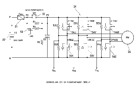
[0003.1 An example of configuration of a conventional
power conversion device applied to drive of the electric
vehicle such as the battery forklift is shown in Figs.
1 to 5. Fig. 1 illustrates an overall configuration of
an inverter for driving a motor of an electric vehicle
having a battery as a power source (power supply) . A
reference sign 50 is a battery for the power supply.
Between a positive electrode end P and a negative electrode
end N of the battery 50, a protective fuse 51, a main
contactor (MC) 52 for shutting off the power supply in
an abnormal condition and an electrolytic capacitor 021
for smoothing the power supply are connected in series.
Date Recue/Date Received 2023-09-14
- 2 -
[0004.] Between a common connection point (P2) of the
fuse 51 and the main contactor 52 and a common connection
point (P3) of the main contactor 52 and the electrolytic
capacitor 021, a charging resistor (a first charging
resistor) R1 for charging the electrolytic capacitor 21
with charge (electric charge) with a long time constant
is connected.
[0005.] A series circuit of a P-channel charging FET 53
and a charging resistor (a second charging resistor) R3
for charging the electrolytic capacitor 021 with charge
with a charging time constant that is shorter than that
of the charging resistor R1 is connected to the charging
resistor R1 in parallel.
[0006.] A discharging resistor R2 for discharging charge
of the electrolytic capacitor 021 when the battery 50
is OFF (when the battery 50 is disconnected) is connected
between a common connection point (a positive electrode
end P3 of the electrolytic capacitor 021) of the charging
resistor R1 and the charging resistor R3 and a negative
electrode end (N) of the electrolytic capacitor C21.
[0007.] Between the positive electrode end (P3) and the
negative electrode end (N) of the electrolytic capacitor
021, an inverter 54 (a power conversion unit) in which
upper phase side FETs 54U, 54V and 54W and lower phase
side FETs 54X, 54Y and 54Z are three-phase
bridge-connected is connected. Each of the FETs 540, 54V,
54W, 59X, 54Y and 59Z is composed of, for instance, an
N-channel MOSFET.
[0008.] A series circuit of a resistor 550 and a resistor
55X is connected to a series circuit of the U-phase FET
Date Recue/Date Received 2023-09-14
- 3 -
54U and the X-phase FET 54X in parallel. A common
connection point of the resistor 55U and the resistor
55X is connected to a common connection point of the U-phase
FET 54U and the X-phase FET 54X.
[0009.] A series circuit of a resistor 55V and a resistor
55Y is connected to a series circuit of the V-phase FET
54V and the Y-phase FET 54Y in parallel. A common
connection point of the resistor 55V and the resistor
55Y is connected to a common connection point of the V-phase
FET 54V and the Y-phase FET 54Y.
[0010.] A series circuit of a resistor 55W and a resistor
55Z is connected to a series circuit of the W-phase FET
54W and the Z-phase FET 54Z in parallel. A common
connection point of the resistor 55W and the resistor
55Z is connected to a common connection point of the W-phase
FET 54W and the Z-phase FET 54Z. AC sides u, v and w of
the inverter 54 are connected to a motor 56.
[0011.] In the drawing, Vp4 indicates a voltage dividing
point voltage of the resistor 55U and the resistor 55X,
Vp 5 indicates a voltage dividing point voltage of the
resistor 55V and the resistor 55Y, and Vp6 indicates a
voltage dividing point voltage of the resistor 55W and
the resistor 55Z, and these voltage dividing point
voltages are input to a CPU constituting a control unit
(not shown) .
[0012.] An example of an upper phase side FET arm gate
drive circuit and a lower phase side FET arm gate drive
circuit of the device of Fig. 1 is shown in Fig. 2. Fig.
2 illustrates, as an example, a configuration of U-phase
and X-phase FET arm gate drive circuits.
Date Recue/Date Received 2023-09-14
- 4 -
[0013.] In Fig. 2, a reference sign 60 denotes a high
withstand voltage IC (or a high voltage IC) (High Voltage
Integrated Circuit; hereinafter, referred to as HVIC)
for driving gates of the U-phase FET 54U and the X-phase
FET 54X.
[0014.] A reference sign 62 denotes a level shifter that
increases a level of a gate control signal (HIN) of a
high side circuit side which is input from a high side
input terminal 61H. An internal circuit 63 at the high
side is connected to an output side of the level shifter
62. A totem-pole circuit in which two n-channel FETs 64Ha
and 64Hb are cascaded (cascade-connected) is connected
to an output side of the internal circuit 63.
[0015.] A reference sign 63L denotes an internal circuit
at a low side which inputs a gate control signal (LIN)
of a low side circuit side which is input from a low side
input terminal 61L. A totem-pole circuit in which two
n-channel FETs 64La and 64Lb are cascaded
(cascade-connected) is connected to an output side of
the internal circuit 63L.
[0016.1 A resistor 65H is connected between the high side
input terminal 61H and a ground (an earth) . A resistor
65L is connected between the low side input terminal 61L
and the ground.
[0017.] A reference sign 70 denotes a gate power supply
that outputs a gate power supply of, e.g. 14V. A capacitor
031 (an upper phase side gate drive power supply capacitor
(a bootstrap capacitor) ) is connected to an output side
of the gate power supply 70 via an anode and a cathode
of a diode Dl. Also, a capacitor C32 (a lower phase side
Date Recue/Date Received 2023-09-14
- 5 -
gate drive power supply capacitor) is connected to the
output side of the gate power supply 70 via an anode and
a cathode of a diode D2.
[0018.] One end (at the diode D1 side) of the capacitor
031 is connected to a ground side end of the totem-pole
circuit configured by the FETs 64Ha and 64Hb.
[0019.] One end (at the diode D2 side) of the capacitor
032 is connected to a ground side end of the totem-pole
circuit configured by the FETs 64La and 64Lb and the
negative electrode end (N) of the battery 50 (not shown) .
[0020.] An output end (a common connection point of the
FETs 6411a and 6411b) of the totem-pole circuit configured
by the FETs 64Ha and 64Hb is connected to the gate of
the U-phase FET 54U via a resistor R11. The ground side
end of the totem-pole circuit configured by the FETs 64Ha
and 64Hb is connected to a source of the U-phase FET 54U
via a resistor R12. A resistor R14 is connected between
the gate and the source of the U-phase FET 54U.
[0021.] An output end (a common connection point of the
FETs 64La and 64Lb) of the totem-pole circuit configured
by the FETs 64La and 64Lb is connected to the gate of
the X-phase FET 54X via a resistor R13. A resistor R15
is connected between the gate and a source of the X-phase
FET 54X.
[0022.] A cathode of a diode D3 is connected to a common
connection point of the ground end of the totem-pole
circuit configured by the FETs 64Ha and 64Hb and the
resistor R12. An anode of the diode D3 is connected to
the negative electrode end (N) of the battery 50 (to the
source of the X-phase FET 54X) .
Date Recue/Date Received 2023-09-14
- 6 -
[0023.] The battery 50 is configured to be freely
connectable and disconnectable.
[0024.] FET arm gate drive circuits for V-phase and
Y-phase and FET arm gate drive circuits for W-phase and
Z-phase are also configured in the same manner as that
in Fig. 2.
[0025.] In the device configured above, the battery 50
is connected, a key switch (not shown) is tuned on and
the electrolytic capacitor 021 is charged, and after the
main contactor 52 is turned on, drive of the inverter
54 is started. Sequence up to the start of the drive of
the inverter 54 will be described below.
[0026.] (1) When the battery 50 is connected and
subsequently the key switch is tuned on, the main contactor
(MC) 52 is turned on. When turning the main contactor
(MC) 52 on, a necessary condition is that when a mechanical
contact (s) of the main contactor 52 is closed, a charging
rush current flows from the battery 50 to the electrolytic
capacitor C21. In order to suppress this charging rush
current to an acceptable peak current value to the
contact (s) of the main contactor 52, it is necessary to
lower a primary and secondary potential difference of
the main contactor 52 then close the contact (s) .
[0027.] Here, a path of the battery 50 a cable the
main contactor 52 the electrolytic capacitor 021 becomes
a circuit composed of LRC by an inductor of the cable,
a cable resistance and a battery internal equivalent
resistance, as shown in Fig. 3.
[0028.] In Fig. 3, a reference sign E is voltage of the
battery 50, a reference sign L is the inductor of the
Date Recue/Date Received 2023-09-14
- 7 -
cable, a reference sign R is the cable resistance and
the battery resistance, and a reference sign Cl is a
capacitance of the electrolytic capacitor C21.
[0029.] A circuit equation is the following.
[0030.] [Expression 1]
di
L----I-Ri+ ¨1 fidt= E
dt
[0031.] The circuit equation is the above (1).
[0032.] Here, since L is small, L is neglected for
calculation, then a current i when the main contactor
52 is closed is the following.
[0033.] [Expression 2]
E 1 )
I = --eXp( ___________________ (2)
CiR
[0034.] Here, the lower the voltage difference is, the
lower the peak current value is. From this, lowering the
primary and secondary potential difference of the main
contactor 52 is good for suppressing the inrush current
of the contactor.
[0035.] Froma timepointwhen thebattery 50 is connected,
the electrolytic capacitor C21 is charged through the
charging resistor R1, and if the primary and secondary
potential difference of the main contactor 52 is not equal
to or less than a predetermined voltage difference when
the key switch is turned on, in order to further charge
the electrolytic capacitor C21, the charging FET 53 is
turned on, and a charging operation is performed through
the charging resistor R3. Then, when the potential
Date Recue/Date Received 2023-09-14
- 8 -
difference between the electrodes of the contactor becomes
equal to or less than the predetermined value, the main
contactor 52 is closed.
[0036.1 (2) When the closing of the main contactor 52
is completed, the inverter 54 can start operating.
[0037.] However, gate drive power supply energy is not
stored (accumulated) in the upper phase side FET arm gate
drive circuit (e.g. the U-phase FET arm gate drive circuit
in Fig. 2) of the inverter 54. That is, in Fig. 5 showing
a relationship between a stray capacitance (or a parasitic
capacitance) of each terminal of the U-phase FET 54U and
the U-phase FET arm gate drive circuit, since a charge-pump
operation (a charging operation of the capacitor C31)
has not been performed even once, at this time point,
an output of the totem-pole circuit configured by the
FETs 69Ha and 69Hb for driving the high side arm in the
HVIC 60 is OFF at both of a source side and a sink side.
[0038.] In Fig. 5, same elements or components as those
of Fig. 2 are denoted by the same reference signs, but
the diode D3, the resistors R13 and R15, the level shifter
62 and the resistors 65H and 65L in the HVIC 60 in Fig.
2 are omitted.
[0039.] Crss of the U-phase FET 54U indicates a drain-gate
capacitance (a feedback capacitance or a reverse transfer
capacitance) , and Cgs of the U-phase FET 54U indicates
a gate-source capacitance (an input capacitance) .
[0040.1 In the U-phase FET 59U, the high side arm driving
FETs 64Ha and 64Hb of the HVIC 60 are in the OFF state.
Therefore, if a gate-source voltage Vgs is charged with
charge (electric charge) due to noise etc. from the outside
Date Recue/Date Received 2023-09-14
- 9 -
in this state, there is no means to prevent malfunction
other than the discharge capability of the resistor R14
between the gate and the source of the U-phase FET 54U.
[0041.] (3) Charging sequence of the gate drive power
supply energy of the upper phase side (U-phase) FET arm
gate drive circuit and the lower phase side (X-phase)
FET arm gate drive circuit
(3-1) Charging sequence of the gate drive power supply
energy of the X-phase FET arm gate drive circuit (see
Fig. 4 showing the configuration of the gate drive circuit
which is similar to Fig. 2)
Regarding the charging of the gate drive power supply
energy of the X-phase FET arm gate drive circuit, at a
time point when the gate power supply 70 is established,
the gate drive power supply capacitor C32 is charged by
a circuit of the gate power supply 70 the diode D2
the capacitor 032 OV. This charging is always performed
because a continuously charging circuit is configured
regardless of ON/OFF of the main circuit FET.
[0042.] (3-2) Charging sequence of the gate drive power
supply energy of the U-phase FET arm gate drive circuit
(3-2-1) Voltage of the positive electrode end P3 of the
electrolytic capacitor C21 is a battery voltage, and
becomes a nominal voltage 72 V or greater. Although the
capacitor C31 is charged by current flowing to the
capacitor 031 from the gate power supply 70, as its charging
circuit, by continuity (i.e. ON) of the lower phase side
FET (X-phase), the following charging circuit is formed,
then the capacitor C31 is charged.
Date Recue/Date Received 2023-09-14
- 10 -
[0043.] The gate power supply 70 the diode D1 the
capacitor C31 the resistor R12 the X-phase FET 54X
(3-2-2) An opportunity to turn on the X-phase FET 54X
is a time when the inverter 54 is operated. As the inverter
operation, normally, such a complementary PWM operation
that when the upper phase side arm drive is ON, the lower
phase side arm drive is OFF, and when the upper phase
side arm drive is OFF, the lower phase side arm drive
is ON is performed. However, when the capacitor C31 is
not charged, the upper phase side FET cannot be turned
on. When the lower phase side FET (X-phase) is ON-driven
next, the capacitor C31 is charged.
[0044.] When the capacitor C31 is charged, either the
upper FET or the lower FET (6411a or 64Hb) of the totem-pole
output of the upper phase side FET arm gate drive circuit
is turned on or off according to the operation.
[0045.] (3-2-3) When the inverter 54 is continuously
operated so that the upper and lower arm FETs are
continuously driven by the complementary PWM operation,
since the capacitor C31 is continuously charged when the
lower phase side FET (X-phase) is turned on, the drive
circuit of the upper phase side FET (U-phase) can stably
continue with ON/OFF.
[0046.] Here, as the gate drive circuit of the FET in
the conventional power conversion device, gate drive
circuits described in, for instance, Patent Documents
1 and 2 have been proposed.
CITATION LIST
PATENT DOCUMENT
Date Recue/Date Received 2023-09-14
- 11 -
[0047.]
Patent Document 1: Japanese Unexamined Patent Application
Publication No. 2019-033621
Patent Document 2: Japanese Unexamined Patent Application
Publication No. 2010-200554
SUMMARY OF THE INVENT ION
[0048.] In the above (3-2-2) of BACKGROUND ART, a
drain-source voltage of the lower phase side FET (the
X-phase FET 54X) when the lower phase side FET (the X-phase
FET 54X) is turned on during the inverter operation
abruptly becomes zero volt from a voltage value (Vp4)
applied by the voltage dividing resistors (the potential
dividing resistors) 55U and 55X of Fig. 1.
[0049.1 At this time, an extremelylarge + dvidt is applied
between the drain and the source of the upper phase side
FET (the U-phase FET 54U) .
[0050.] In that case, Crss (the drain-gate capacitance)
and Cgs (the gate-source capacitance) formed inside the
FET depicted in Fig. 5 are brought to a state in which
these Crss and Cgs are connected in series to Vds voltage
applied to the drain-source of the U-phase FET 54U, then
charge (electric charge) is charged in Crss and Cgs.
[0051 . ] In a normal gate drive state, the above-described
gate drive power supply energy (charge voltage of the
capacitor C31) of the U-phase FET 54U exists, and regarding
the output of the totem-pole circuit configured by the
U-phase arm drive FETs 69Ha and 64Hb of the HVIC 60, the
output is operated (sink-operated) in an OFF direction
in the gate drive circuit. Therefore, the charge (the
electric charge) charged in Cgs is discharged to (by or
Date Recue/Date Received 2023-09-14
- 12 -
through) the resistor R11 + the resistor R12, then the
charge of Cgs is not charged. Thus, the gate-source
voltage Vgs does not rise, then the U-phase FET 54U does
not shift to ON-operation.
[0052.] However, at a time of an initial drive (a first
drive), since there is no gate drive power supply energy
of the U-phase FET 54U, the output of the totem-pole circuit
configured by the U-phase arm drive FETs 64Ha and 64Hb
of the HVIC 60 is not operated (in the OFF state) at both
of the source and sink sides. Therefore, because the
charge (the electric charge) charged in Cgs by the applied
Vds can only be discharged through the resistor R14 (high
resistance), depending on the Vds value, Crss, Cgs and
Vgs (th) (a characteristic value of the FET, which is a
threshold value of the gate-source voltage Vgs (at which
a continuity state of the FET is changed (current of the
threshold value or more starts to flow between the drain
and the source) at a certain drain-source voltage), the
upper phase side FET (the U-phase FET 54U) is ON-operated
(which is not in a complete ON-state, but has an
ON-resistance of a certain value or less which is in an
active state) when Vds is applied to the U-phase FET 54U
(= when the lower phase side (X-phase) FET is turned on),
and consequently, an arm short-circuit current may flow
from the terminal P3 power supply to the upper phase side
FET (the U-phase FET 54U) and the lower phase side FET
(the X-phase FET 54X) .
[0053.] Voltage of Cgs can be determined as follows.
When a series combined value of capacitance of the
drain-gate-source is C, C is the following.
Date Recue/Date Received 2023-09-14
- 13 -
[0054.] [Expression 3]
Crs, Cgs
C = = = (3)
Crsa + Cgs
[0055.] When voltage V is applied between the drain and
the source, charge Q stored (accumulated) between the
drain and the source is the following.
[0056.] [Expression 4]
C V Q Crss = Vdg ¨ Cgs = Vgs ...(4)
[0057.] From the above,
[0058.] [Expression 5]
C = V
= = ( 5 )1
VgS C
gs
[0059.] Vgs is the above (5).
[0060.] Further, in a case where as a circuit board (a
substrate) on which the above electronic components are
mounted, a metal base board (a metal base substrate) whose
back surface is a metal plate is used, in addition to
these capacitances between the FET terminals,
capacitances between the base metal and the terminals
affect the characteristics.
[0061.] Here, various stray capacitances (or various
parasitic capacitances) of a case where the U-phase FET
54U and the X-phase FET 54X shown in Figs. 1 and 2 are
mounted on the metal base board (the metal base substrate)
will be described with reference to Fig. 9.
[0062.] In Fig. 9, Batt indicates the battery 50 of Fig.
1, C4 indicates the electrolytic capacitor 021 of Fig.
1.
Date Recue/Date Received 2023-09-14
- 14 -
[0063.] The U-phase FET 54U and the X-phase FET 54X are
mounted on the metal base board (the metal base substrate)
in parallel by soldering.
[0064.] Cl and C5 are gate-source capacitances of the
U-phase FET 54U and the X-phase FET 54X, C2 and C6 are
drain-gate capacitances of the U-phase FET 54U and the
X-phase FET 54X, and C3 and C7 are output capacitances
of the U-phase FET 54U and the X-phase FET 54X.
[0065.] C8 to C12 are capacitances formed by dielectric
constant (or permittivity) of an insulating layer (s)
between the base metal (aluminium) and patterns, and these
capacitances affect the characteristics.
[0066.] Assuming that capacitance characteristics Crss
and Cgs of the upper phase side FET (the U-phase FET 54U)
and the lower phase side FET (the X-phase FET 54X) are
Crss = 105pF and Cgs = 5270pF, a series combined value
C of the both capacitances is calculated as follows.
a series combinedvalueC=105x5270/ (105+5270) =102.9pF
Q = CV = 102.9pFx24v = 2469.6 [pC]
Vgs = Q/Cgs = 2469.6pC/5270pF = 0.46[V]
[0067.] Effects on the gate-source voltage Vgs which are
determined from numerical values of Crss and Cgs are as
described above, but these are based on calculation of
the FET alone.
[0068.] However, as a result of measurement of Vgs in
an actual inverter state (in a state in which the FET
is mounted on the metal base board (the metal base
substrate) ), it rose to about 5V.
[0069.] Because of this, the upper phase side FET (the
U-phase FET 54U) is turned on (ON-operated) , and
Date Recue/Date Received 2023-09-14
- 15 -
consequently, the short-circuit current passes through
the upper and lower FETs for a short period of time.
[0070.] As precaution of this problem, the following
measures exist in the prior arts.
[0071.] (1) Make the parallel resistance R14 between Vgs
shown in Figs. 2 and 5 even lower.
[0072.] , Problem : Regarding the resistor R14, since
a driving circuit consumption current become large when
ON-driving the FET, it is necessary to increase the
capacitance of the upper phase side FET drive power supply
capacitor (the capacitor 031) . Then, since the
consumption current becomes large and also time required
to charge the electric charge becomes longer, there is
a need to increase a minimum ON-electric conductivity
of the lower phase side FET. Consequently, a minimum
operation voltage of the inverter deteriorates.
[0073.] (2) Insert a capacitor in parallel between the
gate and the source of the FET, and increase Cgs and lower
voltage of Cgs.
[0074.] , Problem : The same problem as the above (1)
occurs. Further, in a case where there is a current limit
in the gate drive circuit, since a charging time constant
of Vgs increases when driving the FET gate, transition
period at turn-on and turn-off becomes longer, and an
FET switching loss for the transition period increases,
then heat generation becomes high.
[0075.] Next, an example of a conventional process from
ON of the key switch to start of the inverter operation
of the device of Figs. 1 to 5 will be described with
reference to Figs. 6 and 7. In Fig. 6 showing a flow chart
Date Recue/Date Received 2023-09-14
- 16 -
of the conventional process, the battery 50 of Fig. 1
is connected to the circuit before step Si. Then, at step
Si, the key switch is turned on.
[0076.] Next, at step S2, a judgment is made as to whether
or not the voltage of the positive electrode end P3 of
the electrolytic capacitor C21 of Fig. 1 is 63V or less.
If the judgment result is YES, at step S3, a quick charging
process (the charging FET 53 is turned on) is performed.
[0077.] Subsequently, at step S4, a judgment is made as
to whether or not the voltage of the positive electrode
end P3 is 5V or less and also its state continues for
0.6 seconds. If the judgment result of step S4 is YES,
at step S5, a predetermined quick charging error process
(process in which the main circuit FET (s) of the inverter
and the electrolytic capacitor C21 are judged to be
short-circuited, and this abnormal state is notified to
a host controller (not shown) ) is performed.
[0078.] If the judgment result of step S4 is NO or after
the process of step S5, at step S6, a judgment is made
as to whether or not the voltage of the positive electrode
end P3 is 63V or less and also its state continues for
3.6 seconds.
[0079.] If the judgment result of step S6 is YES, at step
S7, a predetermined quick charging error process (process
in which an error state is notified to the host controller
(not shown) ) is performed.
[0080.] If the judgment result of step S6 is NO or after
the process of step S7, at step S8, a judgment is made
as to whether or not the voltage of the positive electrode
Date Recue/Date Received 2023-09-14
- 17 -
end P3 is 3V or less and also its state continues for
15 seconds.
[0081.] If the judgment result of step S8 is YES, at step
S9, the upper and lower phase FETs are judged to be
short-circuited.
[0082.] If the judgment result of step S2 is NO or the
judgment result of step S8 is NO, at step S10, the main
contactor 52 of Fig. 1 is turnedon, and after the turning-on
of the main contactor 52, at step S11, the operation of
the inverter 54 is started.
[0083.1 According to the conventional process flow of
Fig. 6, the upper and lower phase arms are driven for
the first time by the operation of the inverter at step
S11, and by turning-on of the lower phase side arm FET
(the X-phase FET 54X) , the gate drive power supply
capacitor (the capacitor 031) of the upper phase side
FET armgate drive circuit is charged with charge (electric
charge), then operation of the upper phase arm becomes
possible.
[0084.] Next, operation waveform of each part of the
device and capacitance of the FET when performing the
process along the flow chart of Fig. 6 will be described
with reference to Figs. 7 and 8. Fig. 7 is a time chart
showing operation waveform of only a set of upper and
lower arms of the U-phase and the X-phase. Capacitances
of these U-phase FET and X-phase FET are shown in Fig.
8.
[0085.] In Fig. 8, Batt indicates the battery 50 of Fig.
1, C4 indicates the electrolytic capacitor 021 of Fig.
1. Cl indicates the gate-source capacitance of the
Date Recue/Date Received 2023-09-14
- 18 -
U-phase FET 54U, C5 indicates the gate-source capacitance
of the X-phase FET 54X, 02 indicates the drain-gate
capacitance of the U-phase FET 54U, C6 indicates the
drain-gate capacitance of the X-phase FET 54X, 03
indicates the drain-source capacitance of the U-phase
FET 54U, and 07 indicates the drain-source capacitance
of the X-phase FET 54X.
[0086.1 Vds is the drain-source voltage (voltage between
Vp3 and Vp4) of the U-phase FET. In Fig. 8, operation
of the X-phase FET is illustrated as a relay Si (SW) .
[0087.1 In Fig. 7, (a) is a voltage Vp3 of the positive
electrode end P3 of the electrolytic capacitor 021, which
corresponds to voltage Vp3 in Fig. 8.
[0088.] (b) is the drain-source voltage Vds (the voltage
between Vp3 and Vp4 in Fig. 8) of the upper phase side
U-phase FET.
[0089.] (c) is Vp4 (a drain-source voltage Vds of the
X-phase FET the voltage Vp4 in Figs. 8 and 1) at the
drain side of the lower phase side X-phase FET.
[0090.] (d) is a gate voltage of the U-phase FET.
[0091.] (e) is a power supply voltage of the U-phase gate
drive circuit (a power supply voltage of the upper phase
side FET arm gate drive circuit (the high side totem-pole
circuit of the HVIC 60) ) .
[0092.] (f) is a U-phase gate signal (a PWM signal of
the U-phase FET 54U) .
[0093.] (g) is a gate voltage of the X-phase FET.
[0094.] (h) is a power supply voltage of the X-phase gate
drive circuit (a power supply voltage of the lower phase
Date Recue/Date Received 2023-09-14
- 19 -
side FET arm gate drive circuit (the low side totem-pole
circuit of the HVIC 60) ) .
[0095.] (i) is an X-phase gate signal (a PWM signal of
the X-phase FET 54X) .
[0096.] (j) is the short-circuit current flowing from
the U-phase FET to the X-phase FET.
[0097.] First, at time tl, when thebattery 50 is connected,
a charging current flows from the battery 50 to the
electrolytic capacitor C21 through the fuse 51 and the
charging resistor R1, and a precharging of the
electrolytic capacitor 021 is started, then Vp3 increases
as shown in Fig. 7 (a) .
[0098.] Next, at time t2 (an execution time of the process
at step Si in Fig. 6) , when the key switch is turn on,
the capacitor C32 is charged with charge from the gate
power supply 70 of Fig. 2 through the diode D2, and as
shown in Fig. 7 (h) , the power supply voltage of the X-phase
gate drive circuit (the power supply voltage of the low
side totem-pole circuit of the HVIC 60) rises.
[0099.] At time t3 after a lapse of a predetermined time
after the key switch is turn on at time t2, when the charging
FET 53 is turned on, current flows to the electrolytic
capacitor 021 through the charging FET 53 and the charging
resistor R3, and the quick charge of the electrolytic
capacitor 021 is started. This time t3 is an execution
time of the process at step S3 in Fig. 6.
[0100.] At time t4 at which the voltage Vp3 of the
electrolytic capacitor C21 increases and the potential
difference between the electrodes of the main contactor
52 becomes equal to or less than the predetermined value,
Date Recue/Date Received 2023-09-14
- 20 -
the main contactor 52 is closed. This time t4 is an
execution time of the process at step S10 in Fig. 6.
[0101.1 Next, at time t5 (an execution time of the process
at step Sll in Fig. 6) at which the inverter operation
is started and the U-phase gate signal (the PWM signal)
is input as shown in Fig. 7(f), since the X-phase FET
54X has not been ON-controlled yet, no current flows along
a path shown by a broken arrow in Fig. 4 (showing the
same configuration as that of Fig. 2), then the power
supply voltage of the U-phase gate drive circuit (the
voltage of the gate drive power supply capacitor C31 of
the upper phase side FET arm gate drive circuit) of Fig.
7(e) has not been risen yet. Because of this, as shown
in Fig. 7(d), the gate of the U-phase FET 54U is not ON
at time t5.
[0102.] Next, at time t6, as shown in Fig. 7(i), the
X-phase gate signal (the PWM signal) is input, and the
gate of the X-phase FET 54X is ON as shown in Fig. 7 (g) .
Therefore, the U-phase gate drive power supply capacitor
C31 is charged, and as shown in Fig. 7 (e) , the power supply
voltage of the U-phase gate drive circuit rises.
[0103.] At this time t6, since the U-phase gate signal
is OFF as shown in Fig. 7 (f) , the drain-source voltage
Vds of the U-phase FET 54U rises as shown in Fig. 7 (b) .
And, by dv/dt of this Vds, as shown in Fig. 7(d), the
voltage Vgs is produced between the gate and the source
of the U-phase FET 54U via the drain-gate capacitance
Crss of the U-phase FET 54U denoted by C2 in Fig. 8. Since
this Vgs slightly exceeds the threshold value Vgs (th)
of the gate-source voltage of the U-phase FET 54U, the
Date Recue/Date Received 2023-09-14
- 21 -
drain-source ON-resistance slightly lowers, and
consequently, as shown in Fig. 7 (j ) , the short-circuit
current flows along a path of the drain of the U-phase
FET 54U , the source of the U-phase FET 54U , the drain
of the X-phase FET 59X , the source of the X-phase FET
54X.
[0104.] Although Fig. 7 shows the time chart of only the
set of upper and lower arms of the U-phase and the X-phase,
the inverter has three sets of upper and lower arms of
the U-phase and the X-phase, the V-phase and the Y-phase
and the W-phase and the Z-phase, and these all show the
operation as in Fig. 7.
[0105.] As described above, the conventional control
method shown in Figs. 6 and 7 has a drawback of causing
a malfunction due to the high voltage applied to the upper
phase side FET then leading to the short circuit of the
upper and lower phase arms.
[0106.] In addition, Patent Document 1 describes a
technique in which a driving transistor is separately
provided, a voltage drop of a capacitor of a bootstrap
circuit during a long-time intermittent driving operation
is predicted by fluctuation (variation) of voltage of
a separately provided capacitor, and an output terminal
in a high impedance state is made to be low by the driving
transistor. In the case of this technique of Patent
Document 1, it is necessary to use elements by a large
number of circuit configurations.
[0107.] Further, Patent Document 2 describes a
configuration in which a capacitor of a bootstrap circuit
is charged at startup. However, this configuration is
Date Recue/Date Received 2023-09-14
- 22 -
applied to a case where voltage at a time of start is
high, and as a problem, there is a risk that a malfunction
will occur due to high voltage.
[0108.1 The present invention is an invention that solves
the above problems, and an object of the present invention
is to provide a control device and a control method of
a power conversion device which are capable of preventing
the drawback of causing the malfunction due to the high
voltage applied to the upper phase side FET and leading
to the short circuit of the upper and lower phase arms.
[0109.1 As a control device of a power conversion device
to solve the above problems described herein,
the power conversion device includes: a power conversion
unit in which an upper phase side FET and a lower phase
side FET are bridge-connected between positive and
negative electrode ends of a DC power supply; an
electrolytic capacitor connected to a series circuit of
the upper phase side FET and the lower phase side FET
of the power conversion unit in parallel; a main contactor
interposed on an electric path connecting the positive
electrode end of the DC power supply and a positive
electrode end of the electrolytic capacitor; a first
charging resistor connected to the main contactor in
parallel for charging the electrolytic capacitor with
a set charging time constant; a series circuit of a charging
FET connected to the first charging resistor in parallel
and configured to be ON-controlled after a set time after
a key switch is turned on and a second charging resistor
set to a charging time constant that is shorter than that
of the first charging resistor; an upper phase side FET
Date Recue/Date Received 2023-09-14
- 23 -
arm gate drive circuit configured to drive a gate of the
upper phase side FET of the power conversion unit; a lower
phase side FET arm gate drive circuit configured to drive
a gate of the lower phase side FET of the power conversion
unit; an upper phase side gate drive power supply capacitor
configured to be charged when a gate power supply starts
up by the turning-on of the key switch and also the lower
phase side FET is ON-controlled, and served as a power
supply of the upper phase side FET arm gate drive circuit;
and a lower phase side gate drive power supply capacitor
configured to be charged when the gate power supply starts
up by the turning-on of the key switch and served as a
power supply of the lower phase side FET arm gate drive
circuit, and
the power conversion device is configured so that the
DC power supply is freely connectable and disconnectable,
the control device is configured so that
a value of resistance of the first charging resistor is
set so that in a precharging period until the key switch
is turned on after the DC power supply is brought to a
connecting state, when the upper phase side FET is
controlled to be OFF and the lower phase side FET is
controlled to be ON, a charge voltage value of the
electrolytic capacitor is set so as to be able to limit
a gate-source voltage of the -upper phase side FET to voltage
at which the upper phase side FET is not turned on, and
the control device comprises: a control unit configured
so that when voltage of the electrolytic capacitor is
the set charge voltage value after the key switch is turned
on before the power conversion unit is operated, the lower
Date Recue/Date Received 2023-09-14
- 24 -
phase side FET is controlled to be ON, then the upper
phase side gate drive power supply capacitor is charged,
and after the ON-control of the lower phase side FET,
the charging FET is controlled to be ON, and further,
when a potential difference between both ends of the main
contactor becomes equal to or less than a set value, the
main contactor is turned on, then operation of the power
conversion unit is started.
[0110.] As the control device of the power conversion
device as described herein, the charge voltage value of
the electrolytic capacitor in the precharging period is
set so that each parasitic capacitance generated between
a metal base substrate and terminals of the upper phase
side FET and the lower phase side FET of the power conversion
unit when the upper phase side FET and the lower phase
side FET are mounted on the metal base substrate is taken
into consideration, and a voltage generated between the
gate and a source of the upper phase side FET when an
instantaneous voltage is applied between a drain and the
source of the upper phase side FET is calculated, then
a voltage value transiently applied to the gate-source
voltage Vgs via each parasitic capacitance becomes low
in a sufficiently large range as compared with a voltage
value at which failure detection by continuation of low
voltage between the drain and the source for a certain
time is operated.
[0111.] As a method of controlling a power conversion
device described herein,
the power conversion device includes: a power conversion
unit in which an upper phase side FET and a lower phase
Date Recue/Date Received 2023-09-14
- 25 -
side FET are bridge-connected between positive and
negative electrode ends of a DC power supply; an
electrolytic capacitor connected to a series circuit of
the upper phase side FET and the lower phase side FET
of the power conversion unit in parallel; a main contactor
interposed on an electric path connecting the positive
electrode end of the DC power supply and a positive
electrode end of the electrolytic capacitor; a first
charging resistor connected to the main contactor in
parallel for charging the electrolytic capacitor with
a set charging time constant; a series circuit of a charging
FET connected to the first charging resistor in parallel
and configured to be ON-controlled after a set time after
a key switch is turned on and a second charging resistor
set to a charging time constant that is shorter than that
of the first charging resistor; an upper phase side FET
arm gate drive circuit configured to drive a gate of the
upper phase side FET of the power conversion unit; a lower
phase side FET arm gate drive circuit configured to drive
a gate of the lower phase side FET of the power conversion
unit; an upper phase side gate drive power supply capacitor
configured to be charged when a gate power supply starts
up by the turning-on of the key switch and also the lower
phase side FET is ON-controlled, and served as a power
supply of the upper phase side FET arm gate drive circuit;
and a lower phase side gate drive power supply capacitor
configured to be charged when the gate power supply starts
up by the turning-on of the key switch and served as a
power supply of the lower phase side FET aim gate drive
circuit, and
Date Recue/Date Received 2023-09-14
- 26 -
the power conversion device is configured so that the
DC power supply is freely connectable and disconnectable,
the method comprises:
setting a value of resistance of the first charging
resistor so that in a precharging period until the key
switch is turned on after the DC power supply is brought
to a connecting state, when the upper phase side FET is
controlled to be OFF and the lower phase side FET is
controlled to be ON, a charge voltage value of the
electrolytic capacitor is set so as to be able to limit
a gate-source voltage of the upper phase side FET to voltage
at which the upper phase side FET is not turned on, and
as a step by a control unit,
when voltage of the electrolytic capacitor is the set
charge voltage value after the key switch is turned on
before the power conversion unit is operated, controlling
the lower phase side FET to be ON, then charging the upper
phase side gate drive power supply capacitor, and
after the ON-control of the lower phase side FET,
controlling the charging FET to be ON, and further, when
a potential difference between both ends of the main
contactor becomes equal to or less than a set value, turning
on the main contactor, then start operation of the power
conversion unit.
(1) According to the invention described herein, the
charge voltage value of the electrolytic capacitor in
the precharging period is set to be lower than that of
the conventional device or method. And, when the voltage
of the electrolytic capacitor is the set charge voltage
value that is lower than that of the conventional device
Date Recue/Date Received 2023-09-14
- 27 -
or method, the lower phase side FET is controlled to be
ON, then the upper phase side gate drive power supply
capacitor is charged. Therefore, the applied voltage
dv/dt between the drain and the source of the upper phase
side FET, which is generated when the lower phase side
FET is first ON-controlled (is first turned on), can be
reduced.
[0112.] With this, the charge (the electric charge)
charged along the path of the drain-gate capacitance
(Crss) of the upper phase side FET the gate-source
capacitance Cgs of the upper phase side FET is reduced,
then the value of the gate-source voltage Vgs can be lowered.
As a result, the malfunction of the short-circuit between
the upper and lower phase arms can be prevented.
(2) According to the invention described herein, since
the charging voltage value of the electrolytic capacitor
in the precharging period is set by taking into
consideration each stray capacitance (or each parasitic
capacitance) in the state in which the FETs are mounted
on the metal base substrate and by calculating the
gate-source voltage of the upper phase side FET when an
instantaneous voltage is applied between the drain and
the source of the upper phase side FET, setting accuracy
of the charging voltage value of the electrolytic
capacitor can be increased, and erroneous failure
detection can be avoided.
BRIEF DESCRIPTION OF THE DRAWINGS
[0113.]
Fig. 1 is a configuration of a main circuit of an inverter
to which the present invention is applied.
Date Recue/Date Received 2023-09-14
-28 -
Fig. 2 is a circuit diagram of gate drive circuits of
U-phase and X-phase of Fig. 1.
Fig. 3 is an explanatory drawing showing a calculation
method of an inrush current when closing a main contactor
of Fig. 1.
Fig. 4 is a circuit diagram showing a charge path of a
capacitor C31 of Fig. 2.
Fig. 5 is FET gate drive circuits illustrated by
simplifying Figs. 2 and 4 in order to explain a stray
capacitance (or a parasitic capacitance) of each terminal
of FET.
Fig. 6 is a flow chart of process of a conventional control
device.
Fig. 7 is a time chart showing operation waveform of each
part by the conventional process.
Fig. 8 is an explanatory drawing showing each capacitance
of a U-phase FET and an X-phase FET.
Fig. 9 is an explanatory drawing showing each parasitic
capacitance in a case where the U-phase FET and the X-phase
FET are mounted on a metal base board (a metal base
substrate).
Fig. 10 is a flow chart of process of an embodiment of
the present invention.
Fig. 11 is a flow chart of process of another embodiment
of the present invention.
Fig. 12 is a time chart showing operation waveform of
each part by process of the present embodiment.
EMBODIMENTS FOR CARRYING OUT THE INVENTION
[0114.] Although embodiments of the present invention
will be described below with reference to the drawings,
Date Recue/Date Received 2023-09-14
- 29 -
the present invention is not limited to the following
embodiments. In the present embodiments, a power
conversion device such as an inverter/converter using
power MOSFETs etc. in a main control circuit is configured
so that especially when a power supply voltage is high,
an occurrence of a malfunction (an unintended
ON-operation) of an upper phase side FET of a main circuit
is prevented.
[0115.] Further, an FET gate drive circuit (s) is
configured so that when resuming operation of the
inverter/converter (the power conversion device) after
continuation of a long-time stop period of the
inverter/converter (the power conversion device) , the
above malfunction is prevented.
[0116.] The embodiment of the present invention applied
to the power conversion device of Figs. 1 to 5 will be
described below. A value of resistance of the resistor
R1, which is a first charging resistor in Fig. 1, is set
so that in a precharging period until the key switch is
turned on after the battery 50 is brought to the connecting
state, when the upper phase side FET, e.g. the U-phase
FET 54U, is controlled to be OFF and the lower phase side
FET, e.g. the X-phase FET 54X, is controlled to be ON,
a charge voltage value of the electrolytic capacitor 021
is set so as to be able to limit the gate-source voltage
of the U-phase FET 54U to voltage at which the U-phase
FET 54U is not turned on.
[0117.] Further, the control unit is configured so that
when the voltage of the electrolytic capacitor C21 is
the set charge voltage value after the key switch is turned
Date Recue/Date Received 2023-09-14
- 30 -
on before the inverter 54 is operated, the lower phase
side FET, e.g. the X-phase FET 54X, is controlled to be
ON, then the upper phase side gate drive power supply
capacitor (the capacitor C31) is charged, and after the
ON-control of the lower phase side FET (the X-phase FET
54X) , the charging FET 53 is controlled to be ON, and
further, when the potential difference between both ends
of the main contactor 52 becomes equal to or less than
the set value, the main contactor 52 is closed (turned
on), then operation of the inverter 54 is started.
[0118.] In the configuration of the power conversion
device of Fig. 1, when, e.g. a 72V battery, is applied,
a precharging voltage value of the electrolytic capacitor
021 before the key switch is turned on after the battery
50 is connected, which was about 50V in the conventional
configuration, is lowered to about 20V in the present
embodiment.
[0119.] This precharging voltage value of the
electrolytic capacitor C21 is set so that each stray
capacitance (or each parasitic capacitance) generated
between a metal base substrate and terminals of the upper
phase side FET (e.g. the U-phase FET 54U) and the lower
phase side FET (e.g. the X-phase FET 54X) of the inverter
54 when the upper phase side FET and the lower phase side
FET are mounted on the metal base substrate is taken into
consideration, and a voltage generated between the gate
and the source of the upper phase side FET when an
instantaneous voltage is applied between the drain and
the source of the upper phase side FET is calculated,
then a voltage value transiently applied to the
Date Recue/Date Received 2023-09-14
- 31 -
gate-source voltage Vgs via each parasitic capacitance
becomes low in a sufficiently large range as compared
with a voltage value at which failure detection by
continuation of low voltage between the drain and the
source for a certain time is operated.
[0120.] Next, an example of a process of the present
embodiment fromON of the key switch to start of the inverter
operation of the device of Figs. 1 to 5 will be described
with reference to Figs. 10 and 12. In Fig. 10 showing
a flow chart of the process of the present embodiment,
the battery 50 of Fig. 1 is connected to the circuit before
step S21. Then, at step S21, the key switch is turned
on.
[0121.1 Next, at step S22, a judgment is made as to whether
or not the voltage of the positive electrode end P3 of
the electrolytic capacitor 021 of Fig. 1 is 10V or less.
If the judgment result is YES, at step S23, a quick charging
process (the charging FET 53 is turned on) is performed.
[0122.] Subsequently, at step S29, a judgment is made
as to whether or not the voltage of the positive electrode
end P3 is 5V or less and also its state continues for
0.6 seconds. If the judgment result of step S24 is YES,
at step S25, a predetermined quick charging error process
(process in which the main circuit FET (s) of the inverter
and the electrolytic capacitor 021 are judged to be
short-circuited, and this abnormal state is notified to
a host controller (not shown) ) is performed.
[0123.1 If the judgment result of step S24 is NO or after
the process of step S25, at step S26, a judgment is made
as to whether or not the voltage of the positive electrode
Date Recue/Date Received 2023-09-14
- 32 -
end P3 is 10V or less and also its state continues for
3.6 seconds.
[0124.] If the judgment result of step S26 is YES, at
step S27, a predetermined quick charging error process
(process in which an error state is notified to the host
controller (not shown) ) is performed.
[0125.] If the judgment result of step S26 is NO or after
the process of step S27, at step S28, a judgment is made
as to whether or not the voltage of the positive electrode
end P3 is 3V or less and also its state continues for
seconds.
[0126.] If the judgment result of step S28 is YES, at
step S29, the upper and lower phase FETs are judged to
be short-circuited.
15 [0127.] If the judgment result of step S22 is NO or the
judgment result of step S28 is NO, at step S30, the gate
of the lower phase side FET, e.g. the X-phase FET 54X,
is ON-controlled (is controlled to be on) only for Zmsec,
and after that, at step S31, the gate of the X-phase FET
54X is OFF-controlled (is controlled to be off) .
[0128.] Next, at step S32, a judgment is made as to whether
or not the voltage Vp3 of the positive electrode end P3
of the electrolytic capacitor C21 is 63V or less. If the
judgment result is YES, at step S33, the charging FET
53 of Fig. 1 is turned on again, and the quick charging
of the electrolytic capacitor 021 is performed.
[0129.1 Next, at step S34, a judgment is made as to whether
or not the voltage Vp3 is 63V or less and also its state
continues for 3.6 seconds. If the judgment result of step
S34 is YES, at step S35, a quick charging error process
Date Recue/Date Received 2023-09-14
- 33 -
such as a process in which an abnormal state is notified
to the host controller (not shown) is performed.
[0130.] If the judgment result of step S34 is NO or after
the process of step S35, at step S36, the main contactor
52 of Fig. 1 is turned on, and after the turning-on of
the main contactor 52, at step S37, the inverter 54 is
operated.
[0131.] At a time of this step S37, since the upper phase
(U-phase) side FET arm gate drive power supply capacitor
(the capacitor C31) is charged with charge (electric
charge), the upper phase (U-phase) arm does not
malfunction such as the arm short-circuit operation.
[0132.] Fig. 12 shows operation waveform of each part
of only a set of upper and lower arms of the U-phase and
the X-phase when the process along the flow chart of Fig.
10 is performed.
[0133.] In Fig. 12, (a) is the voltage Vp3 of the positive
electrode end P3 of the electrolytic capacitor C21, which
corresponds to the voltage Vp3 in Fig. 8.
[0134.] (b) is the drain-source voltage Vds (the voltage
between Vp3 and Vp4 in Fig. 8) of the upper phase side
U-phase FET.
[0135.] (c) is Vp4 (the drain-source voltage Vds of the
X-phase FET : the voltage Vp4 in Figs. 8 and 1) at the
drain side of the lower phase side X-phase FET.
[0136.] (d) is the gate voltage of the U-phase FET.
[0137.] (e) is the power supply voltage of the U-phase
gate drive circuit (the power supply voltage of the upper
phase side FET arm gate drive circuit (the high side
totem-pole circuit of the HVIC 60) ) .
Date Recue/Date Received 2023-09-14
- 34 -
[0138.] (f) is the U-phase gate signal (the PWM signal
of the U-phase FET 54U) .
[0139.] (g) is the gate voltage of the X-phase FET.
[0140.] (h) is the power supply voltage of the X-phase
gate drive circuit (the power supply voltage of the lower
phase side FET arm gate drive circuit (the low side
totem-pole circuit of the HVIC 60) ) .
[0141.] (i) is the X-phase gate signal (the PWM signal
of the X-phase FET 54X) .
[0142.] (j) is the short-circuit current flowing from
the U-phase FET to the X-phase FET.
[0143.] First, at time tl, when thebattery 50 is connected,
a charging current flows from the battery 50 to the
electrolytic capacitor 021 through the fuse 51 and the
charging resistor R1, and the precharging of the
electrolytic capacitor 021 is started, then Vp3 increases
as shown in Fig. 12(a) .
[0144.] In the present embodiment, since the charging
resistor R1 is set so that the precharging voltage value
of the electrolytic capacitor C21 of Fig. 1 becomes low,
as shown in Fig. 12(a) , (b) and (c) , voltage waveforms
move (increase) at Vp3, Vds and Vp4 that are lower than
the voltage waveforms shown by broken lines according
to the conventional control method.
[0145.] At time t2a (an execution time of the process
at step S21 in Fig. 10) , when the key switch is turn on,
the capacitor C32 is charged with charge from the gate
power supply 70 of Fig. 2 through the diode D2, and as
shown in Fig. 12 (h) , the power supply voltage of the X-phase
Date Recue/Date Received 2023-09-14
-35 -
gate drive circuit (the power supply voltage of the low
side totem-pole circuit of the HVIC 60) rises.
[0146.] When the precharging of the electrolytic
capacitor C21 is not completed (in Fig. 10, the judgment
result of step S22 is YES) after the key switch is turn
on at time t2a, the charging FET 53 of Fig. 1 is turned
on, and processes of steps S23 to S29 in Fig. 10 are
performed.
[0147.] Next, at time t2b (an executiontime of theprocess
at step S30 in Fig. 10), as shown in Fig. 12(g), the gate
of the X-phase FET 54X is ON-controlled. With this,
current flows along the path shown by a broken arrow in
Fig. 4, and the upper phase (U-phase) side gate drive
power supply capacitor (the capacitor 031) is charged,
then as shown in Fig. 12(e), the power supply voltage
of the U-phase gate drive circuit rises.
[0148.] Next, at time t3a (an executiontime of the process
at step S31 in Fig. 10), as shown in Fig. 12(g), the gate
of the X-phase FET 54X is OFF-controlled.
[0149.] Next, at time t3b (an executiontime of the process
at step S33 in Fig. 10), the charging FET 53 is turned
on, and current flows to the electrolytic capacitor 021
through the charging FET 53 and the charging resistor
R3, and the quick charge of the electrolytic capacitor
021 is performed.
[0150.] Next, at time t4 at which the voltage Vp3 of the
electrolytic capacitor C21 increases and the potential
difference between the electrodes of the main contactor
52 becomes equal to or less than the predetermined value,
Date Recue/Date Received 2023-09-14
- 36 -
the main contactor 52 is closed. This time t4 is an
execution time of the process at step S36 in Fig. 10.
[0151.] Subsequently, at time t5 (an execution time of
the process at step S37 in Fig. 10) of the operation start
time of the inverter 54, as shown in Fig. 12 (f) , when
the U-phase gate signal (the PWM signal) is input, since
the power supply voltage (the voltage of the capacitor
031) of the U-phase gate drive circuit has already been
established at this time t5 as shown in Fig. 12 (e) , as
shown in Fig. 12 (d) , the gate signal (the gate voltage)
of the U-phase FET 54U is normally generated.
[0152.] With this, the U-phase FET 54U is ON-controlled,
and as shown in Fig. 12 (b), the drain-source voltage Vds
of the U-phase FET 54U correctly becomes zero (normal
ON-operation is performed) .
[0153.] Next, at time t6, as shown in Fig. 12(1) and (f) ,
when the X-phase gate signal (the PWM signal) is on and
the U-phase gate signal (the PWM signal) is off, as shown
in Fig. 12(g) and (d) , the gate of the X-phase FET 54X
is turned on and the gate of the U-phase FET 54U is turned
off.
[0154.] During a period for which the U-phase FET 54U
is off and the X-phase FET 54X is on, since the voltage
of the capacitor 031 is established, the upper phase
(U-phase) side FET arm gate drive circuit (the high side
totem-pole circuit of the HVIC 60 in Fig. 5) performs
an OFF-output operation (sink-operation), and the
gate-source voltage (charge of the input capacitance Cgs)
of the U-phase FET 54U is discharged through the resistor
R11, the lower side FET of the high side totem-pole circuit
Date Recue/Date Received 2023-09-14
- 37 -
and the resistor R12 of Fig. 5. Therefore, voltage that
exceeds the threshold value Vgs (th) of the gate-source
voltage of the U-phase FET 54U is not generated, then
the upper and lower arm short-circuit current, as shown
at time t7 at which ON/OFF of the FETs of the U-phase
and the X-phase is changed, does not flow.
[0155.] Although Fig. 12 shows the time chart of only
the set of upper and lower arms of the U-phase and the
X-phase, the inverter has three sets of upper and lower
arms of the U-phase and the X-phase, the V-phase and the
Y-phase and the W-phase and the Z-phase, and these all
show the operation as in Fig. 12.
[0156.] As described above, according to the present
embodiment, the applied voltage dv/dt between the drain
and the source of the upper phase side FET, which is
generated when the lower phase side FET is first
ON-controlled (is first turned on) , can be reduced.
[0157.] With this, the charge (the electric charge)
charged along the path of the drain-gate capacitance
(Crss) of the upper phase side FET , the gate-source
capacitance Cgs of the upper phase side FET is reduced,
then the value of the gate-source voltage Vgs can be lowered.
As a result, the malfunction of the short-circuit between
the upper and lower phase arms can be prevented.
[ 0 15 8 . ] Further, since the charging voltage value of the
electrolytic capacitor C21 in the precharging period is
set by taking into consideration each stray capacitance
(or each parasitic capacitance) in the state in which
the FETs are mounted on the metal base substrate and by
calculating the gate-source voltage of the upper phase
Date Recue/Date Received 2023-09-14
- 38 -
side FET when an instantaneous voltage is applied between
the drain and the source of the upper phase side FET,
setting accuracy of the charging voltage value of the
electrolytic capacitor can be increased, and erroneous
failure detection can be avoided.
[0159.] Next, a process of another embodiment of the
present invention will be described. There is a case where
after closing the main contactor 52 (after time t9 in
Fig. 12) as in the process at step S36 in Fig. 10, the
inverter operation is not performed for a while. In such
a situation, OFF-operation of the upper phase side FET
continues. That is, since the upper phase side FET gate
drive circuit continues with a continuous operation, in
order to recharge the upper phase (U-phase) side gate
drive power supply capacitor (the capacitor 031) before
a lapse of a certain time (time required for energy (the
voltage of the capacitor C31) of the upper phase (U-phase)
side gate drive power supply to be consumed/discharged
and decreased) , the lower phase side FET is made to be
turned on for a short time. With this, since energy
recharging of the upper phase (U-phase) side gate drive
power supply capacitor (the capacitor C31) is performed,
rise of Vgs of the FET caused by the fact that the gate
drive circuit does not perform OFF-operation, which tends
to occur at the beginning of the inverter operation, is
prevented.
[0160.] A flow chart of this process is shown in Fig.
11. Fig. 11 is a process executed during stop of the
inverter operation while the main contactor 52 is closed.
At step S41, a judgment is made as to whether or not the
Date Recue/Date Received 2023-09-14
- 39 -
gate of the upper phase side FET (the U-phase FET 54U)
is turned on. If the judgment result is NO, at step S42,
a judgment is made as to whether or not the elapsed time
is Xsec or less. If the judgment result of step S42 is
YES, at step S43, a counter is incremented (count-up).
If the judgment result of step S42 is NO, at step S44,
a judgment is made as to whether or not the elapsed time
is Ysec or less.
[0161.] If the judgment result of step S44 is YES, at
step S45, a counter is incremented (count-up). If the
judgment result of step S94 is NO, at step S46, the gate
of the lower phase side FET (the X-phase FET 54X) is
ON-controlled (is controlled to be on) only for Zmsec,
and after that, at step S47, the gate of the lower phase
side FET (the X-phase FET 54X) is turned off.
[0162.] If the judgment result of step S41 is YES or after
the processes of steps S43, S45 or S47, the routine is
returned to the first step S41, and the process of Fig.
11 is repeatedly executed.
[0163.] According to the above embodiment, even in the
case where the inverter operation is not performed for
a while after closing the main contactor 52, since the
upper phase side FET gate drive circuit power supply energy
(the capacitor C31) is recharged by turning on the lower
phase side FET at certain intervals, rise of Vgs of the
FET caused by the fact that the gate drive circuit does
not perform OFF-operation is suppressed, and the
malfunction of the short-circuit between the upper and
lower phase arms can be prevented.
[0164.] The following aspects are also disclosed herein:
Date Recue/Date Received 2023-09-14
- 40 -
[1] A control device of a power conversion device,
the power conversion device including:
a power conversion unit in which an upper phase
side FET and a lower phase side FET are
bridge-connected between positive and negative
electrode ends of a DC power supply;
an electrolytic capacitor connected to a series
circuit of the upper phase side FET and the lower
phase side FET of the power conversion unit in
parallel;
a main contactor interposed on an electric path
connecting the positive electrode end of the
DC power supply and a positive electrode end
of the electrolytic capacitor;
a first charging resistor connected to the main
contactor in parallel for charging the
electrolytic capacitor with a set charging time
constant;
a series circuit of a charging FET connected to
the first charging resistor in parallel and
configured to be ON-controlled after a set time
after a key switch is turned on and a second
charging resistor set to a charging time
constant that is shorter than that of the first
charging resistor;
an upper phase side FET arm gate drive circuit
configured to drive a gate of the upper phase
side FET of the power conversion unit;
Date Recue/Date Received 2023-09-14
- 41 -
a lower phase side FET arm gate drive circuit
configured to drive a gate of the lower phase
side FET of the power conversion unit;
an upper phase side gate drive power supply
capacitor configured to be charged when a gate
power supply starts up by the turning-on of the
key switch and also the lower phase side FET
is ON-controlled, and served as a power supply
of the upper phase side FET arm gate drive
circuit; and
a lower phase side gate drive power supply
capacitor configured to be charged when the gate
power supply starts up by the turning-on of the
key switch and served as a power supply of the
lower phase side FET arm gate drive circuit,
and
the power conversion device configured so that
the DC power supply is freely connectable and
disconnectable,
the control device configured so that
a value of resistance of the first charging
resistor is set so that in a precharging period
until the key switch is turned on after the DC
power supply is brought to a connecting state,
when the upper phase side FET is controlled to
be OFF and the lower phase side FET is controlled
to be ON, a charge voltage value of the
electrolytic capacitor is set so as to be able
to limit a gate-source voltage of the upper phase
Date Recue/Date Received 2023-09-14
- 42 -
side FET to voltage at which the upper phase
side FET is not turned on, and
the control device comprising:
a control unit configured so that when voltage
of the electrolytic capacitor is the set charge
voltage value after the key switch is turned
on before the power conversion unit is operated,
the lower phase side FET is controlled to be
ON, then the upper phase side gate drive power
supply capacitor is charged, and after the
ON-control of the lower phase side FET, the
charging FET is controlled to be ON, and further,
when a potential difference between both ends
of the main contactor becomes equal to or less
than a set value, the main contactor is turned
on, then operation of the power conversion unit
is started.
[2] The control device of the power conversion device
of aspect 1, wherein
the charge voltage value of the electrolytic
capacitor in the precharging period is set so
that each parasitic capacitance generated
between a metal base substrate and terminals
of the upper phase side FET and the lower phase
side FET of the power conversion unit when the
upper phase side FET and the lower phase side
FET are mounted on the metal base substrate is
taken into consideration, and a voltage
generated between the gate and a source of the
Date Recue/Date Received 2023-09-14
- 43 -
upper phase side FET when an instantaneous
voltage is applied between a drain and the source
of the upper phase side FET is calculated, then
a voltage value transiently applied to the
gate-source voltage Vgs via each parasitic
capacitance becomes low in a sufficiently large
range as compared with a voltage value at which
failure detection by continuation of low
voltage between the drain and the source for
a certain time is operated.
[3] A method of controlling a power conversion device,
the power conversion device including:
a power conversion unit in which an upper phase
side FET and a lower phase side FET are
bridge-connected between positive and negative
electrode ends of a DC power supply;
an electrolytic capacitor connected to a series
circuit of the upper phase side FET and the lower
phase side FET of the power conversion unit in
parallel;
a main contactor interposed on an electric path
connecting the positive electrode end of the
DC power supply and a positive electrode end
of the electrolytic capacitor;
a first charging resistor connected to the main
contactor in parallel for charging the
electrolytic capacitor with a set charging time
constant;
Date Recue/Date Received 2023-09-14
- 44 -
a series circuit of a charging FET connected to
the first charging resistor in parallel and
configured to be ON-controlled after a set time
after a key switch is turned on and a second
charging resistor set to a charging time
constant that is shorter than that of the first
charging resistor;
an upper phase side FET arm gate drive circuit
configured to drive a gate of the upper phase
side FET of the power conversion unit;
a lower phase side FET arm gate drive circuit
configured to drive a gate of the lower phase
side FET of the power conversion unit;
an upper phase side gate drive power supply
capacitor configured to be charged when a gate
power supply starts up by the turning-on of the
key switch and also the lower phase side FET
is ON-controlled, and served as a power supply
of the upper phase side FET arm gate drive
circuit; and
a lower phase side gate drive power supply
capacitor configured to be charged when the gate
power supply starts up by the turning-on of the
key switch and served as a power supply of the
lower phase side FET arm gate drive circuit,
and
the power conversion device configured so that
the DC power supply is freely connectable and
disconnectable,
the method comprising:
Date Recue/Date Received 2023-09-14
- 45 -
setting a value of resistance of the first charging
resistor so that in a precharging period until
the key switch is turned on after the DC power
supply is brought to a connecting state, when
the upper phase side FET is controlled to be
OFF and the lower phase side FET is controlled
to be ON, a charge voltage value of the
electrolytic capacitor is set so as to be able
to limit a gate-source voltage of the upper phase
side FET to voltage at which the upper phase
side FET is not turned on, and
as a step by a control unit,
when voltage of the electrolytic capacitor is the
set charge voltage value after the key switch
is turned on before the power conversion unit
is operated, controlling the lower phase side
FET to be ON, then charging the upper phase side
gate drive power supply capacitor, and
after the ON-control of the lower phase side FET,
controlling the charging FET to be ON, and
further, when a potential difference between
both ends of the main contactor becomes equal
to or less than a set value, turning on the main
contactor, then start operation of the power
conversion unit.
Date Recue/Date Received 2023-09-14