Note: Descriptions are shown in the official language in which they were submitted.
WO 2022/192167
PCT/US2022/019227
PARTIAL-RESONANT CONVERTERS FOR PV APPLICATIONS
BACKGROUND OF THE DISCLOSURE
Field of the Disclosure
[00um] Embodiments of the present disclosure relate generally to power
conversion,
and, in particular, to partial-resonant power converters.
Description of the Related Art
[0002] DC-AC power converters play an indispensable role in various electrical
power applications, such as converting DC from renewable energy resources to
power-grid compliant AC. Topologies for these power converters are designed
with
various considerations, including cost and efficiency. For example, improving
the
power density of a converter can contribute to a lower final cost of
production.
[0003] Therefore, there is a need in the art for improved power converter
topologies.
SUMMARY OF THE DISCLOSURE
[0004] In accordance with at least some aspects of the disclosure a partial-
resonant
converter is provided herein and comprises a partial resonant link formed by a
magnetizing link inductor connected in parallel with a first capacitor on a
primary
winding side of a transformer and a second capacitor on a secondary winding
side
of the transformer, a pair of series connected switches coupled across the
magnetizing link inductor and the first capacitor, and
a plurality of forward
conducting bidirectional blocking switches that connect an input source and an
output load to the magnetizing link inductor during operation.
[0oos] In accordance with at least some aspects of the disclosure a partial-
resonant
converter is provided herein and comprises a partial resonant link formed by a
magnetizing link inductor connected in parallel with a first capacitor on a
primary
winding side of a transformer and a second capacitor on a secondary winding
side
of the transformer, a pair of series connected switches coupled across the
magnetizing link inductor and the first capacitor, and
a plurality of forward
1
CA 03211624 2023- 9-8
WO 2022/192167
PCT/US2022/019227
conducting bidirectional blocking switches that connect an input source and an
output load to the magnetizing link inductor during buck-boost mode of
operation.
[0006] These and other features and advantages of the present disclosure may
be
appreciated from a review of the following detailed description of the present
disclosure, along with the accompanying figures in which like reference
numerals
refer to like parts throughout.
BRIEF DESCRIPTION OF THE DRAWINGS
[0007] So that the manner in which the above recited features of the present
disclosure can be understood in detail, a more particular description of the
disclosure, briefly summarized above, may be had by reference to embodiments,
some of which are illustrated in the appended drawings. It is to be noted,
however,
that the appended drawings illustrate only typical embodiments of this
disclosure
and are therefore not to be considered limiting of its scope, for the
disclosure may
admit to other equally effective embodiments.
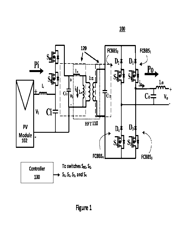
[mos] Figure 1 is a block diagram of a power converter in accordance with one
or
more embodiments of the present disclosure;
[0oos] Figure 2 is a block diagram of a controller in accordance with one or
more
embodiments of the present disclosure;
[0010] Figure 3 is a block diagram of a power converter in accordance with one
or
more embodiments of the present disclosure;
prin Figure 4 is a block diagram of a controller in accordance with one or
more
embodiments of the present disclosure;
[0012] Figure 5 is a block diagram of a power converter in accordance with one
or
more embodiments of the present disclosure; and
[0013] Figure 6 is a block diagram of a controller in accordance with one or
more
embodiments of the present disclosure.
2
CA 03211624 2023- 9-8
WO 2022/192167
PCT/US2022/019227
DETAILED DESCRIPTION
[0014] Figure 1 is a block diagram of a power converter 100 in accordance with
one
or more embodiments of the present disclosure. This diagram only portrays one
variation of the myriad of possible system configurations. The present
disclosure can
function in a variety of power generation environments and systems.
[0015] The power converter 100 is a partial-resonant DC-to-single-phase AC
converter with galvanic isolation. The power converter 100 comprises an input
switch bridge comprising two back-to-back metal¨oxide¨semiconductor field-
effect
transistors, (MOSFETs), (or bidirectional-conducting unidirectional-blocking)
Soo and
So, (which may in other embodiments be wide-bandgap devices). The So drain and
a first terminal of an inductor Li are each coupled to a first terminal of a
capacitor a;
a second terminal of the inductor Li and a second terminal of the capacitor a
are
respectively coupled to positive and negative terminals of a DC input, such as
a
photovoltaic (PV) module 102. A partial-resonant link 120 is formed by a small
magnetizing inductance LM of a high-frequency transformer (HFT) 110 along with
very small AC capacitors CLi and CL2 (it is assumed that leakage inductance of
the
transformer 110 - represented in Figure 1 as Ls - is negligible). In some
embodiments, CL2 may be a reflected capacitance. The magnetizing inductance
Lim
(and any leakage inductance Ls) and the AC capacitor CLi are each coupled
across
the series combination of the switches Soo, So, and the capacitor C.
[0016] The secondary winding of the transformer 110 is coupled across an
output
bridge which connects the output load to the inductive link. The output bridge
comprises four forward-conducting bidirectional-blocking (FCBB) switches. In
some
embodiments, such as the embodiment depicted in Figure 1, each FCBB switch may
be composed of a series combination of a switch and a diode (switches Si, S2,
S3, S4
and corresponding diodes Di, D2, 03, Da forming corresponding FCBB switches
FCBBSi, FCBBS2, FCBBS3, FCBBS4 in Figure 1); in other embodiments, a forward-
conducting bidirectional-blocking switch may be composed of back-to-back
switches
(or AC switch), or a switch with bidirectional capability. The switches FCBBS2
and
FCBBS4 are coupled to one another in series, and the switches FCBBSi and
3
CA 03211624 2023- 9-8
WO 2022/192167
PCT/US2022/019227
FCBBS3 are coupled to one another in series; these series combinations are
coupled across the secondary winding of the transformer 110. The transformer
110
has a 1:n turns ratio, and the capacitor CL2 is also present across the
transformer
secondary winding.
[0017] A first terminal of an output capacitor Co is coupled to the drain of
the switch
FCBBSi and to a first terminal of an output inductor Lo; a second terminal of
the
output capacitor Co is coupled to the drain of the switch FCBBS2. Output
terminals
(i.e., a second terminal of the input Lo and the second terminal of the
capacitor Co)
may be coupled to any suitable system or device, such as a single-phase AC
power
line. Gate terminals of each of the switches Soo, So, and FCBBS1-FCBBS4, are
coupled to a controller 130 for operatively controlling the switches.
[0018] The power converter 100 functions in buck-boost mode of operation and
transfers power entirely through the link inductor, which is charged and
discharged
each cycle. The power converter 100 has a lower total switch-count than
conventional four-quadrant inductive-link converters performing similar
functions
(e.g., universal power converters). In contrast to these conventional
converters that
utilize four-quadrant link operation, where the link current can be positive
and
negative, the power converter 100 restricts the link current to one direction,
thereby
allowing the power converter 100 to have a smaller number of switches and a
simpler control algorithm. Further, the power converter 100 does not utilize
any
switches around the transformer 110, in contrast to topologies used in a solid-
state
transformer (SST) applications. The topology of the power converter 100
improves
the power density of the converter over conventional topologies such as four-
quadrant inductive-link converters and SST converters, and thereby enables a
lower
final cost of production than for conventional topologies.
[0019] In one or more embodiments, the transformer turns ratio 1:n may be 1:9,
the
inductance Ls may be negligible, and the power converter components may have
values on the order of: Cu=1nF; CL2=CL1/n2=0.01234nF (where n=9), Co=1.8uF;
L0=30uH; a=13.2mH, Liv=1.8uH, and Ls=2nH.
4
CA 03211624 2023- 9-8
WO 2022/192167
PCT/US2022/019227
[0020] Figure 2 is a block diagram of a controller 130 in accordance with one
or
more embodiments of the present disclosure. The controller 130 comprises
support
circuits 204 and a memory 206, each coupled to a central processing unit (CPU)
202. The CPU 202 may comprise one or more conventionally
available
microprocessors or microcontrollers; alternatively, the CPU 202 may include
one or
more application specific integrated circuits (ASICs). In other embodiments,
the
CPU 202 may be a microcontroller comprising internal memory for storing
controller
firmware that, when executed, provides the controller functionality described
herein.
[0021] The support circuits 204 are well known circuits used to promote
functionality
of the CPU 202. Such circuits include, but are not limited to, a cache, power
supplies, clock circuits, buses, input/output (I/O) circuits, and the like.
The controller
130 may be implemented using a general-purpose computer that, when executing
particular software, becomes a specific purpose computer for performing
various
embodiments of the present disclosure.
[0022] The memory 206 may comprise random access memory, read only memory,
removable disk memory, flash memory, and various combinations of these types
of
memory. The memory 206 is sometimes referred to as main memory and may, in
part, be used as cache memory or buffer memory. The memory 206 generally
stores the operating system (OS) 208, if necessary, of the controller 130 that
can be
supported by the CPU capabilities. In some embodiments, the OS 208 may be one
of a number of commercially available operating systems such as, but not
limited to,
LINUX, Real-Time Operating System (RTOS), and the like.
[0023] The memory 206 may store various forms of application software, such as
a
converter control module 210 for controlling operation of the power converter
100
when executed by the controller 130. The memory 206 may further store a
maximum power point tracking (MPPT) module 212 that, when executed by the
controller 130, determines an operating point for biasing the PV module 102 at
its
maximum power point (MPP).
CA 03211624 2023- 9-8
WO 2022/192167
PCT/US2022/019227
[0024] The memory 206 may additionally store a database 214 for storing data
related to the operation of the power converter 100.
[0025] Figure 3 is a block diagram of a power converter 300 in accordance with
one
or more embodiments of the present disclosure. This diagram only portrays one
variation of the myriad of possible system configurations. The present
disclosure can
function in a variety of power generation environments and systems.
[0026] The power converter 300 is a partial-resonant DC-to-three-phase AC
converter with galvanic isolation. Analogous to the power converter 100, the
power
converter 300 comprises an input switch bridge comprising two back-to-back
MOSFETs, (or bidirectional-conducting unidirectional-blocking) Soo and So
(which
may in other embodiments be wide band gap devices), where the So drain is
coupled to a first terminal of an inductor Li and to a first terminal of a
capacitor C. A
second terminal of the inductor Li and a second terminal of the capacitor Ci
are
respectively coupled to positive and negative terminals of a DC input, such as
the
PV module 102. A partial-resonant link 320 is formed by a very small AC
capacitors
CLi and CL2 (which in some embodiments may be a reflected capacitance) along
with a small magnetizing inductance LM of a HFT 310 (it is assumed that
leakage
inductance of the transformer 310 - represented in Figure 3 as Ls - is
negligible).
The capacitor CLi is further coupled across the series combination of the
switches
Soo, SO and the capacitor C.
[0027] The secondary winding of the transformer 310 is coupled across an
output
bridge that connects the output load to the inductive link. The output bridge
comprises six forward-conducting bi-directional-blocking (FCBB) output
switches
FCBBSi- FCBBS6 In some embodiments, such as the embodiment depicted in
Figure 3, each forward-conducting bidirectional-blocking switch may be
composed of
a series combination of a switch and a diode (switches Si, S2, S3, S4, S5, S6
and
corresponding diodes Di, D2, D3, Da, Ds, Deforming corresponding forward-
conducting
bi-directional-blocking switches FCBBSi , FCBBS2, FCBBS3, FCBBS4, FCBBSs,
FCBBS6 in Figure 3); in other embodiments, a forward-conducting bidirectional-
blocking switch may be composed of back-to-back switches (or AC switch), or a
6
CA 03211624 2023- 9-8
WO 2022/192167
PCT/US2022/019227
switch with bidirectional capability. The switches FCBBSi and FCBBS4 are
coupled
to one another in series, the switches FCBBS2 and FCBBS5 are coupled to one
another in series, and the switches FCBBS3 and FCBBS6 are coupled to one
another in series; these series combinations are each coupled across the
secondary
winding of the transformer 310. The transformer 310 has a 1:n turns ratio, and
the
capacitor CL2 is also present across the transformer secondary winding.
[0028] An output capacitor Coca is coupled between the drain terminals of the
switches FCBBSi and FCBBS3; to a first terminal of an output inductor Loa; an
output
capacitor Cobc is coupled between the drain terminals of the switches FCBBS2
and
FCBBS3; and an output capacitor Coab is coupled between the drain terminals of
the
switches FCBBSi and FCBBS2. The output inductor Loa is coupled between the
drain terminal of the switch FCBBSi and a first output terminal a; an output
inductor
Lob is coupled between the drain terminal of the switch FCBBS2 and a second
output
terminal b; and an output inductor Loc is coupled between the drain terminal
of the
switch FCBBS3 and a third output terminal c. The output terminals a, b, and c
may
be coupled to any suitable system or device, such as a three-phase AC power
line.
Gate terminals of each of the switches Soo, So, and FCBBSi-FCBBS6, are coupled
to
a controller 330 for operatively controlling the switches.
[0029] The power converter 300 functions in buck-boost mode of
operation and
transfers power entirely through the link inductor, which is charged and
discharged
each cycle. The power converter 300 has a lower total switch-count than
conventional four-quadrant inductive-link converters performing similar
functions
(e.g., universal power converters). In contrast to these conventional
converters that
utilize four-quadrant link operation, where the link current can be positive
and
negative, the power converter 300 restricts the link current to one direction,
thereby
allowing the power converter 300 to have a smaller number of switches and a
simpler control algorithm. Further, the power converter 300 does not utilize
any
switches around the transformer 310, in contrast to topologies used in SST
applications. Further in contrast to conventional topologies, the topology of
the
power converter 300 removes the need for an electrolytic capacitor, employs a
7
CA 03211624 2023- 9-8
WO 2022/192167
PCT/US2022/019227
simpler application control with only one processor; can be installed in
increments of
one; eliminates the high cost associated with double frequency ripple as power
increases; and enables flexibility in developing multi-input/multi-output
products such
as three-phase water pump or three-phase motor drive applications. The
topology
of the power converter 300 improves the power density of the converter over
conventional topologies, such as universal power converters and SST
converters,
and thereby enables a lower final cost of production than for conventional
topologies.
[0030] In one or more embodiments, the transformer turns ratio 1:n may be 1:9,
the
inductance Ls may be negligible, and the power converter components may have
values on the order of: Cu=2nF; CL2=Cu/n2= 0.125nF (where n=9); L,=33uH;
C,=50uF, Lm=3.2uH, Ls=2nH, Coa=2uF, Cob=2uF, C0G=2uF, Loa=100uH, Lob=100uH,
L0c=100u H.
[0031]
Figure 4 is a block diagram of a controller 330 in accordance with one
or
more embodiments of the present disclosure. Analogous to the controller 130,
the
controller 330 comprises support circuits 304 and a memory 306 each coupled to
a
CPU 302, the memory 306 storing various forms of application software such as
a
converter control module 410 for controlling operation of the power converter
300
when executed by the controller 330.
[0032]
Figure 5 is a block diagram of a power converter 500 in accordance with
one or more embodiments of the present disclosure. This diagram only portrays
one
variation of the myriad of possible system configurations. The present
disclosure can
function in a variety of power generation environments and systems.
[0033]
The power converter 500 is a partial-resonant DC-to-single-phase AC
converter with galvanic isolation and suppressed double-frequency ripple. The
power converter 500 comprises the topology of the power converter 100 along
with
an extra bridge ¨ called a ripple bridge ¨ coupled across the output bridge of
forward-conducting bi-directional-blocking switches FCBBS1¨FCBBS4 to handle
double-frequency ripple.
The ripple bridge comprises forward-conducting
8
CA 03211624 2023- 9-8
WO 2022/192167
PCT/US2022/019227
bidirectional-blocking switches FCBBS5¨FCBBS8 (switches S5, S6, Sr. S8 and
corresponding diodes D5, D5, D7, D8 forming corresponding forward-conducting
bi-
directional-blocking switches FCBBS5, FCBBS6, FCBBS7, FCBBSs in Figure 5)
coupled in a bridge configuration, with a small capacitor Crp coupled between
the
midpoints of each bridge leg.
[0034] As with the power converters 100 and 300, the power converter 500
functions
only in buck-boost mode of operation and transfers power entirely through the
link
inductor, which is charged and discharged each cycle, and has a lower switch-
count
than four-quadrant inductive-link conventional converters performing similar
functions. Further in contrast to conventional single-phase DC-AC topologies
without suppressing the double frequency ripple, the topology of the power
converter
500 removes the need for a bulky electrolytic capacitor, eliminates the high
cost
associated with double frequency ripple as power increases; and enables
flexibility
in developing multi-input/multi-output products.
[0035] In one or more embodiments, the transformer turns ratio 1:n may be 1:9,
the
inductance Ls may be negligible, and the power converter components may have
values on the order of: Cu=1nF; CL2=Cu/n2=0.01234nF (where n=9); Co=1.8uF;
Lo=30uH; Li=100uH; Ci=24uF, Crp=10uF; Lm=1.8uH, Ls=2nH.
[0036] Figure 6 is a block diagram of a controller 530 in accordance with one
or
more embodiments of the present disclosure. Analogous to the controllers 130
and
330, the controller 530 comprises support circuits 604 and a memory 606 each
coupled to a CPU 602. The memory 606 stores various forms of application
software such as a converter control module 610 for controlling operation of
the
power converter 500 when executed by the controller 530.
[0037] While the foregoing is directed to embodiments of the present
disclosure,
other and further embodiments of the disclosure may be devised without
departing
from the basic scope thereof.
9
CA 03211624 2023- 9-8