Note: Descriptions are shown in the official language in which they were submitted.
CA 03212502 2023-09-01
WO 2022/191752 PCT/SE2022/050179
1
DESCRIPTION
Title of the Invention:
SYSTEM AND METHOD OF PRODUCING MONOCRYSTALLINE LAYERS ON
A SUBSTRATE
Technical Field
[0001] The invention relates generally to growth of monocrystals or
monocrystalline
layers on a substrate. Specifically, the invention relates to sublimation
growth of high-
quality monocrystalline layers by using the sublimation sandwich method. More
specifically, the invention relates to a new configuration for growth of high-
quality
monocrystalline layers by using the sublimation sandwich method.
Background Art
[0002] In recent years, there has been an increasing demand for the
improvement of
energy efficiency of electronic devices capable of operation at high power
levels and high
temperatures. Silicon (Si) is currently the most commonly used semiconductor
for power
devices. In recent decades, significant progress of the performance of Si-
based power
electronic devices has been made. However, with Si power device technology
maturing, it
becomes more and more challenging to achieve innovative breakthroughs using
this
technology. With a very high thermal conductivity (about 4.9 W/cm), high
saturated
electron drift velocity (about 2.7x10 cm/s) and high breakdown electric field
strength
(about 3 MV/cm), silicon carbide (SiC) is a suitable material for high
temperature, high
voltage and high-power applications.
[0003] The most common technique used for the growth of SiC monocrystals is
the
technique of Physical Vapor Transport (PVT). In this growth technique, the
seed crystal
and a source material are both placed in a reaction crucible which is heated
to the
sublimation temperature of the source and in a manner that produces a thermal
gradient
between the source and the marginally cooler seed crystal. The typical growth
temperature
is ranging from 2200 C to 2500 C. The process of crystallization lasts
typically for 60-
100 hours, SiC monocrystal obtained (herein being named as SiC boule or SiC
ingot)
during that time has the length of 15-40 mm. After growth, the SiC boule is
processed by a
series of wafering steps, mainly including slicing, polishing and cleaning
processes, until a
CA 03212502 2023-09-01
WO 2022/191752 PCT/SE2022/050179
2
batch of SiC wafers are produced. The SiC wafers should be usable for being
the
substrates, on which SiC monocrystalline layer with well controllable doping
and several
to several tens of micrometers in thickness can be deposited by chemical vapor
deposition
(CVD).
[0004] The sublimation sandwich method (SSM) is another variant of the
physical
vapor transport (PVT) growth. Instead of a SiC powder as source material, the
source is a
monolithic SiC plate of either mono- or polycrystalline structure, which is
very beneficial
for controlling the temperature uniformity. The distance between the source
and the
substrate is short for direct molecular transport (DMT), typically 1 mm, which
has the
positive effect that the vapor species do not react with the graphite walls.
The typical
growth temperature of SSM is about 2000 C, which is lower than that of PVT.
Such lower
temperature can help obtain higher crystal quality of SiC monocrystals or
monocrystalline
layers than that in PVT case. During the growth, the growth pressure is kept
at vacuum
condition, around 1 mbar, in order to achieve high growth rate, around 150
p.m/h. Since the
thickness of the source is typically 0.5 mm, the grown SiC layer has about the
same
thickness, which is thinner than that of PVT grown boules which typically are
15-50 mm
long. Therefore, the obtained sample using SSM can be regarded as either a SiC
mini-
boule from the perspective of bulk growth or a super-thick SiC epitaxial layer
from the
perspective of epitaxy.
[0005] In SSM, a source and a seed are loaded in a carbon crucible, so that
a small
gap between the source and seed is formed. As revealed in the paper "Effect of
Tantalum
in Crystal Growth of Silicon Carbide by Sublimation Close Space Technique",
Furusho et
al., Jpn. J. Appl. Phys. Vol. 40 (2001) pp. 6737-6740 and US 7,918,937 B2, the
seed is
loaded above the source, with the support of a spacer in the middle. In the
prior art, for
example, as shown in Figs. 1 and 2, the shape of the spacer is usually ring-
like, with an
inner cutout of either square shape or circular shape, depending on the
sample. The
disadvantage of this shape is the full coverage of the sample edge, leading to
significant
loss of material usage area.
[0006] Another problem encountered when producing epitaxial layers on a
substrate
is the formation of defects and associated prismatic stacking faults
propagating into the
epitaxial layer in the grown surface. Surface morphological defects are
generally classified
CA 03212502 2023-09-01
WO 2022/191752 PCT/SE2022/050179
3
in accordance with their physical appearance. Thus, such defects have been
classified as
"comet", "carrot" and "triangular" defects based on their appearance under a
microscope.
Carrot defects are roughly carrot-shaped features in the surface of the
silicon carbide film.
The features are aligned along the step flow direction of the film and are
characteristically
longer than the depth of the layer in which they are formed. The presence of
such
crystalline defects in silicon carbide films may degrade the performance of or
even totally
destroy electronic devices fabricated in the films, depending on the type,
location, and
density of the defects. The ring-like shape of the spacer mentioned above also
brings about
the higher probability of the formation of the above-mentioned crystalline
defects
originating from the ring edge especially at the upstream side, since the
growth may be
disturbed by the spacer contacted with the substrate edge.
[0007] An additional disadvantage of the use of the ring-like shape of the
spacer is
that the substrate backside at the edge area contacted with the spacer may
have higher
sublimation rate than the area not contacting the spacer. Such non-uniform
backside
sublimation of the substrate results in the unwanted material loss at the
substrate edge and
increases the total thickness of the finished substrate in a non-uniform
manner.
[0008] Thus, there is a need to improve the known systems and methods to
overcome the deficiencies and disadvantages mentioned above.
Summary of Invention
[0009] With the foregoing and other objects in view there is provided, in
accordance
with a first aspect of the present disclosure, a system for producing an
epitaxial
monocrystalline layer on a substrate comprising: an inner container defining a
cavity for
accommodating a source material and the substrate; an insulation container
arranged to
accommodate the inner container therein; an outer container arranged to
accommodate the
insulation container and the inner container therein; and heating means
arranged outside
the outer container and configured to heat the cavity, wherein the inner
container
comprises a plurality of spacer elements arranged to support the substrate at
a
predetermined distance above a solid monolithic source material, wherein each
spacer
element comprises a base portion and a top portion, wherein at least part of
the top portion
tapers towards an apex arranged to contact the substrate.
CA 03212502 2023-09-01
WO 2022/191752 PCT/SE2022/050179
4
[0010] The at least partially tapering spacer elements towards an apex or
point
minimizes the contact surface with the substrate. It has been found that this
not only
increases the available growth surface on the substrate, but also reduces the
formation of
crystalline defects in the grown surface since the contact area between spacer
and substrate
giving rise to such defect formation is minimized. For the same reason, non-
uniform
backside sublimation is also reduced.
[0011] In one embodiment, the top portion tapers from the base portion to
the apex.
With a shape tapering along the whole extension of spacer element, the
manufacturing
process is facilitated, e.g. through laser cutting to achieve optimal spacer
elements.
Preferably, the spacer elements have a shape chosen from a pyramid, a cone, a
tetrahedron
and a prism.
[0012] In one embodiment, each spacer element has a height, and the base
portion
has a transverse width, wherein the ratio between the height and the
transverse width is
from 1:3 to 3:1. Preferably, the height of each spacer element is about 0.7-
1.4 mm and the
transverse width is smaller than or equal to 2.5 mm. the chosen range ensures
optimal
stability and spacing between the source and the substrate.
[0013] In one embodiment, a ratio between a surface area of the apex and a
surface
area of the base portion is from 1:1000 to 1:5. Preferably, the surface area
of the apex is
about 100 [tm2.
[0014] In one embodiment, the spacer elements are regularly distributed
about the
circumference of the substrate.
[0015] In one embodiment, the spacer elements are made of tantalum,
niobium,
tungsten, hafnium, silicon carbide, graphite and/or rhenium. The material
chosen ideally
withstands the high temperatures without deformation and without reacting with
or
otherwise affecting the growth of the epitaxial layer on the substrate.
[0016] In one embodiment, the inner container is cylindrical having an
inner
diameter in the range 100-500 mm, preferably 150-300 mm, and wherein the
substrate and
the source material are disk-shaped. The cylindrical shape facilitates optimal
temperature
CA 03212502 2023-09-01
WO 2022/191752
PCT/SE2022/050179
distribution in the cavity and over the source and substrate and the range
corresponds to
standard wafer sizes in semiconductor devices.
[0017] In one embodiment, the system further comprises a heating body made
of
high-density graphite arranged below the inner container. The heating body
allows for
coupling with the heating means to provide improved heating and optimal
temperature
distribution in the cavity.
[0018] In one embodiment, the surface area of the source material is
greater than or
equal to the surface area of the substrate. The greater or equal surface area
of the source
ensures optimal exposure of the entire growth surface of the substrate and
facilitates
positioning of the spacer elements on the source material.
[0019] In one embodiment, the system further comprises a carbon getter
arranged in
the inner container.
[0020] In a second aspect of the present disclosure, there is provided a
method of
producing an epitaxial monocrystalline layer on a substrate comprising:
providing an inner container defining a cavity for accommodating a source
material
and the substrate;
arranging a solid monolithic source material in the cavity;
arranging the substrate at a predetermined distance above source material by
using a
plurality of spacer elements, wherein each spacer element comprises a base
portion and a
top portion, wherein at least part of the top portion tapers towards an apex,
arranged to
contact the substrate;
arranging the inner container within an insulation container;
arranging the insulation container and the inner container an outer container;
providing heating means outside the outer container to heat the cavity;
evacuating the cavity to a predetermined low pressure;
introducing an inert gas into the cavity;
raising the temperature in the cavity to a predetermined growth temperature by
the
heating means;
maintaining the predetermined growth temperature in the cavity until a
predetermined thickness of the epitaxial monocrystalline silicon carbide layer
on the
CA 03212502 2023-09-01
WO 2022/191752 PCT/SE2022/050179
6
substrate has been achieved; and
cooling the substrate.
[0021] In one embodiment, the spacer elements are regularly distributed
about the
circumference of the substrate.
Brief Description of Drawings
[0022] The invention is now described, by way of example, with reference to
the
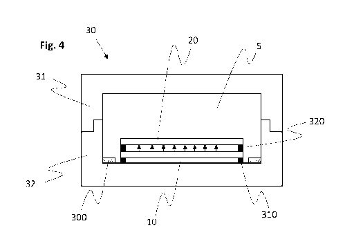
accompanying drawings, in which:
Figs. 1 and 2 show a schematic illustrations of spacer configurations known
from prior art;
Fig. 3 shows a schematic cross-sectional view of a system for producing an
epitaxial
monocrystalline layer on a substrate according to one embodiment of the
present
disclosure;
Fig. 4 shows a schematic cross-sectional view of an inner container with a
source material
and a substrate arranged therein according to one embodiment of the present
disclosure;
Fig. 5 shows a schematic illustration of a spacer element according to one
embodiment of
the present disclosure;
Fig. 6 shows a schematic illustration of an arrangement of spacer elements
according to
one embodiment of the present disclosure;
Fig. 7 shows a diagram of temperature versus time during the growth process;
Fig. 8 shows a flow chart illustrating steps of a method according to one
embodiment of
the present disclosure;
Fig. 9 shows the appearance of a grown SiC sample produced in accordance with
the
present disclosure; and
Figs. 10a and 10b illustrate the crystal quality evaluation using Raman
spectroscopy and
X-ray diffraction (XRD) spectroscopy for a 1.5 mm thick 4H-SiC monocrystalline
epitaxial layer with 150 mm in diameter, manufactured in accordance with the
present
disclosure.
Description of Embodiments
[0023] In the following, a detailed description of a system for producing
an epitaxial
monocrystalline layer on a substrate according to the present disclosure is
presented. In the
drawing figures, like reference numerals designate identical or corresponding
elements
CA 03212502 2023-09-01
WO 2022/191752 PCT/SE2022/050179
7
throughout the several figures. It will be appreciated that these figures are
for illustration
only and are not in any way restricting the scope of the invention.
[0024] One objective of the present invention is to provide a new type of
spacers in
SSM which can realize the growth nearly on the entire seed, whilst minimizing
the
occupation area of the spacers on the seed surface. The spacers are made of
tantalum with
a pyramidal, cylindrical or conical shape and a small size (<2.5 mm in the
base and 0.7-1.4
mm height). In practical, three of such spacers are loaded on the source
surface, and the
seed is loaded on the spacers.
[0025] Fig. 3 is a schematic illustration of the system 100 designed to
facilitate
sublimation epitaxy using the above mentioned polycrystal SiC plate as the
source material
10, which enables the growth of a monocrystal or monocrystalline SiC layer.
The source
material 10 and the substrate 20 are arranged in a cavity of an inner
container 30 in a face-
down configuration, i.e., with the substrate 20 arranged above the source
material 10. The
inner container 30 is arranged within an insulation container 50, which
insulation container
50 in turn is arranged in an outer container 60. The inner container 30 may be
supported on
container supports (not shown) which in turn are on the top of a bottom part
of insulation
container 50. A heating body 40 may optionally be arranged below the inner
container 30.
Outside said outer container 60 there are heating means 70, which can be used
to heat the
cavity of said inner container 30.
[0026] According to one embodiment the heating means 70 comprises an
induction
coil for radiofrequency heating. Said outer container 60 is in this example a
quartz tube and
said insulation container 50 and said inner container 30 are cylindrical and
made of an
insulating graphite foam and high-density graphite, respectively. The heating
means 70 is
used to heat the container and by this sublime the source material 10. The
heating means
70 is movable in a vertical direction in order to adjust the temperature and
thermal gradient
in the inner container 30. The temperature gradient between the source
material 10 and
substrate 20 can also be altered by varying the properties of the inner
container 30, such as
the thicknesses of the upper part 31 and the lower part 32 (see Fig. 4) as is
known in the
art. Additionally, there are pumps for evacuating the inner container (not
shown), i.e. to
provide a pressure between about 10' and 10' mbar.
CA 03212502 2023-09-01
WO 2022/191752 PCT/SE2022/050179
8
[0027] Fig. 4 is a schematic illustration of a preferred arrangement of
components
10, 20, 300, 310, 320 within the cavity 5 of the inner container 30. A
substrate 20 is
supported by spacer elements 320 and is arranged above source material 10,
which is
supported by source supports 310. The diameter of the source material 10
should be equal
to or larger than that of the substrate 20. For example, if the substrate 20
has a diameter of
150 mm, the source material 10 should have at least 150 mm, preferably 160 mm
in
diameter. Close to the source material 10, a carbon getter 300 is loaded on
the inner bottom
of the inner container 30. The spacer elements 320, the source support 310 and
the carbon
getter 300 can be made of a material having a melting point higher than 2200
C and
having an ability of forming a carbide layer with carbon species evaporated
from the
source material, such as tantalum, niobium and tungsten.
[0028] The substrate support preferably comprises three spacer elements
320, each
of which having identical shapes. However, substrate supports with different
shapes or
numbers of spacer elements 320 are also contemplated. Referring now to Fig. 5,
there is
shown an embodiment of a spacer element 320 according to the present
disclosure. The
spacer element 320 comprises a base portion 321 and a top portion 322
extending
upwardly from the base portion 321. In order to minimize the contact area with
the
substrate surface, at least part of the top portion 322 of the spacer element
320 tapers
towards a tip or apex 323. Preferably, the spacer element 320 tapers from the
base portion
321 to the apex 323, simplifying the manufacturing process. The preferred
shape of the
spacer element 320 is a pyramid, a cone (shown in Fig. 5), a tetrahedron or a
prism. In the
case of a prism, the apex is understood as the highest edge located opposite
the base
portion. The transverse width or diameter D of the base portion 321 is
preferably 2.5 mm,
and the height H of the spacer is preferably 1 mm, giving a ratio of the
height H to the
transverse width D of 1:2. However, the ratio H:D may be in the range 3:1 to
1:3.
[0029] In order to minimize the contact surface between the apex 323 of the
spacer
elements 320 and the substrate 20, the spacer elements are manufactured by
laser cutting.
With this process, a surface area of the apex 323 of about 10 p.m by 10 p.m,
i.e., about 100
i.tm2 has been achieved. Preferably, the ratio between the surface areas of
the apex 323 and
the base portion 321 is between 1:1000 and 1:5.
CA 03212502 2023-09-01
WO 2022/191752 PCT/SE2022/050179
9
[0030] Fig. 6 shows an example of the arrangement of three spacer elements
320 on
the top of the source material 10. To support the substrate 20 stably, the
three spacer
elements 320 are preferably distributed regularly around the circumference of
the source
material 10 and the substrate 20, e.g., arranged in a manner of forming an
equilateral
triangular configuration.
[0031] The source material 10 is lifted by the source support 310 to form a
gap
between the source material 10 and the bottom of the inner container 30. This
can help
improve the temperature uniformity of the source material 10 by avoiding the
non-uniform
contact between the source material 10 and the bottom of the inner container
30. The man
skilled in the art should know that the source support 310 is not limited to
any special
shape, for example, it can be as identical as the ones shown in Fig.5. It
should be noted that
the requirement of the source support 310 should be as small as possible in
volume,
without the special requirement of the contact area size with the source
material 10. By
comparison, the spacer elements 320 preferably has not only a minimum volume
but also a
sharp end at the apex 323 for the purpose of minimizing the contact area with
the substrate
20.
[0032] As mentioned above, the substrate 20 is to be arranged above the
source
material 10 on the spacer elements 320. To achieve this, the source material
10 is a solid
monolithic plate, sufficiently rigid to enable placement of the spacer
elements 320 on the
source material 10 to support the substrate 20 along a peripheral edge
thereof. In one
embodiment, the source material 10 is a monolithic SiC plate to produce an
epitaxial
monocrystalline SiC layer on the substrate 20 through SSM. However, other
source
materials may also be used in conjunction with the system 100 and method of
the present
disclosure depending on the desired epitaxial layer to be produced, such as
e.g., aluminum
nitride (A1N).
[0033] The method will now be described with reference to a system design
as
described above, but the man skilled in the art knows that the design is only
an example
and that other designs can also be used as long as the desired growth
conditions are
achieved. Fig. 7 schematically illustrates the temperature variation at the
substrate during
the epitaxial sublimation. The growth process comprises a pre-heating phase
401 wherein
the system is set up for example in accordance with the above description, and
the inner
CA 03212502 2023-09-01
WO 2022/191752 PCT/SE2022/050179
container is evacuated using conventional pumping means. A base vacuum level
of lower
than 10' mbar is normally desired. After that, an inert gas like argon is
introduced into the
reactor chamber and the chamber pressure is kept at about 2 mbar. Then, the
whole growth
system is heated up by heating means in the form of radiofrequency (RF) coils
to the
growth temperature.
[0034] The inventors have discovered that the increase of the temperature
is
preferably between 10-50 C/min, and more preferably about 20-30 C/min. Such
a
temperature increase provides a good initial sublimation of the source and
nucleation. The
temperature is raised during the heating phase 402 until a desired growth
temperature 413
in the range 1900-2000 C is reached, typically about 1950 C. When a suitable
growth
temperature 413 has been reached, i.e., a growth temperature which facilitates
a desired
growth rate, the temperature increase is quickly decreased. The man skilled in
the art
knows at which temperatures a desired growth rate is obtained. The temperature
is kept at
this level 413, until an epitaxial layer of desired thickness has been
achieved. The period
following the heating phase is referred to as the growth phase 403, during
this phase the
temperature is preferably kept substantially constant.
[0035] When a desirably thick monocrystalline layer has been produced 414,
the
heating is turned off and the substrate is allowed to cool down, this is
referred to as the
cooling phase 404. The pre-heating and the cooling phase can be optimized in
order to
decrease the production time.
[0036] In the context of the invention the thickness of the grown
monocrystalline
layer is more than 5 [tm, or more preferably thicker than 100 [tm, and most
preferably
thicker than 500 [tm. The maximum thickness of the grown crystal is determined
by the
thickness of the source material 10.
[0037] The method will now be described with reference to a system design
as
described above, but the man skilled in the art knows that the design is only
an example
and that other designs can also be used as long as the desired growth
conditions are
achieved.
CA 03212502 2023-09-01
WO 2022/191752 PCT/SE2022/050179
11
[0038] Fig. 8 illustrates the process flow in this method. In a first step
S100, the
source material 10 and substrate 20 are provided in the cavity 5 of the inner
container 30.
Optionally, in step S102 the carbon getter 300 is arranged in the cavity.
Subsequently, the
spacer elements 320 are arranged between the source material 10 and the
substrate 20. The
growth process comprises a pre-heating phase S106 wherein the system 100 is
evacuated
using conventional pumping means. A base vacuum level of lower than 10' mbar
is
normally desired, preferably between 10' and 10' mbar. After that, an inert
gas,
preferably argon (Ar), is inserted into the cavity 5 to obtain a pressure
lower than 950
mbar, preferably 600 mbar (S108). The system is then heated up (5110). The
inventors
have discovered that the optimal increase of the temperature is preferably in
the range 10-
50 C/min, and more preferably about 20-30 C/min. Such a temperature increase
provides
a good initial sublimation of the source and nucleation. The temperature is
raised until a
desired growth temperature in the range 1900-2000 C is reached, typically
about 1950 C.
When a suitable growth temperature has been reached, i.e., a growth
temperature which
facilitates a desired growth rate, the pressure is slowly decreased to the
growth pressure.
The man skilled in the art knows at which temperatures a desired growth rate
is obtained.
The temperature is kept at this growth temperature, until an epitaxial layer
of desired
thickness has been achieved. The period following the heating phase is
referred to as the
growth phase S104, during this phase the temperature is preferably kept
substantially
constant. In one embodiment, the thickness of the epitaxial layer obtained in
the growth
phase S104 is 1500 p.m.
[0039] When a desirably thick monocrystalline layer has been produced the
heating
is turned off and the substrate is allowed to cool, this is referred to as the
cooling phase
S114. The pre-heating and the cooling phase can be optimized in order to
decrease the
production time.
[0040] Fig. 9 shows the appearance images of grown SiC samples using the
method
according to the present disclosure. A 1.5 mm thick 4H-SiC monocrystalline
layer has
been grown on the 150 mm substrate surface. On the sample surface, only three
marks
(dents) 350 related to the spacer elements 320 can be found. The size is about
3 mm,
slightly larger than the base of the base D of the spacer (2.5 mm). No other
morphological
defects around the marks 350 are triggered.
CA 03212502 2023-09-01
WO 2022/191752
PCT/SE2022/050179
12
[0041] Figs. 10a and 10b illustrate the crystal quality evaluation using
Raman
spectroscopy and X-ray diffraction (XRD) spectroscopy for a 1.5 mm thick 4H-
SiC
monocrystalline epitaxial layer with 150 mm in diameter, manufactured
according to the
inventive method. Fig. 10a shows the Raman peaks with wavenumbers of 204 cm',
610
cm', 776 cm' and 968 cm', which correspond to Folded Transversal Acoustic
(FTA),
Folded Longitudinal Acoustic (FLA), Folded Transversal Optical (FTO), and
Folded
Longitudinal Optical (FLO) peaks of 4H-SiC. Fig. 10b shows the XRD rocking
curve of
(0008) plane for this sample. The full width at half maximum (FWHM) value is
about 18
arc second, which indicates a high quality of 4H-SiC monocrystal.
[0042] Although the present disclosure has been described in detail in
connection
with the discussed embodiments, various modifications may be made by one of
ordinary
skill in the art within the scope of the appended claims without departing
from the
inventive idea of the present disclosure. Further, the method can be used to
produce more
than one layer in the same cavity as is readily realized by the man skilled in
the art.
[0043] All the described alternative embodiments above or parts of an
embodiment
can be freely combined without departing from the inventive idea as long as
the
combination is not contradictory.