Note: Descriptions are shown in the official language in which they were submitted.
WO 2022/236380
PCT/AU2022/050458
1
"Device for interacting with electromagnetic radiation"
Cross-Reference to Related Applications
[0001] The present application claims priority from Australian Provisional
Patent
Application No 2021901438 filed on 14 May 2021, the contents of which are
incorporated herein by reference in their entirety.
Technical Field
[0002] This disclosure relates to chips, and methods for manufacturing chips,
that
interact with electromagnetic radiation.
Background
[0003] A wide range of antennas and other devices that absorb electromagnetic
radiation are available for various different applications scenarios but
challenges still
remain for their design. In particular, as the frequency of electromagnetic
radiation that
is to be absorbed by the devices increases, conventional designs become
ineffective.
That is, the amount of energy from the electromagnetic radiation absorbed by
the
devices becomes insufficient mainly because metal conductors used in
conventional
antennas become lossy at high frequencies and therefore lead to a reduction in
effectiveness.
[0004] In the terahertz (THz) range, there are theoretical designs of new
materials and
devices that show in simulations that they absorb electromagnetic radiation,
but their
manufacturing remains challenging. As a result, few experimental results and
few
physical example antennas are available. Therefore, there is a need for an
absorber that
is effective, with tuneability or reconfigurability, and that has a design
that can be
realised physically.
[0005] Any discussion of documents, acts, materials, devices, articles or the
like
which has been included in the present specification is not to be taken as an
admission
CA 03218961 2023- 11- 14
WO 2022/236380
PCT/AU2022/050458
2
that any or all of these matters form part of the prior art base or were
common general
knowledge in the field relevant to the present disclosure as it existed before
the priority
date of each of the appended claims.
[0006] Throughout this specification the word "comprise", or variations such
as
"comprises" or "comprising", will be understood to imply the inclusion of a
stated
element, integer or step, or group of elements, integers or steps, but not the
exclusion of
any other element, integer or step, or group of elements, integers or steps.
Summary
[0007] This disclosure provides a device that interacts with electromagnetic
radiation
in the sub-terahertz wavelength range, for example. The disclosed device
comprises a
dielectric layer overlayed by a bi-layer of a metallic conductive material,
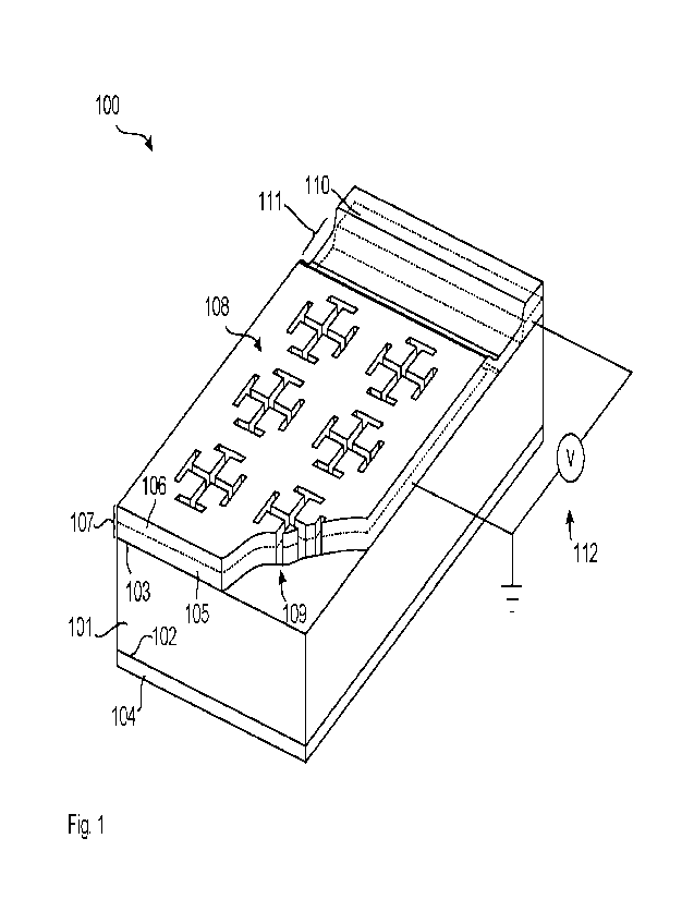
such as gold,
for frequency-selective interaction, such as absorption, and graphene for
tuneability.
The bi-layer is patterned together to provide a superimposed pattern on the
conductive
metal and the graphene. As a result, the chip provides the interaction, with
the tuneable
amplitude and frequency by adjusting a bias voltage applied on the graphene,
and can
be manufactured by depositing the conductive metal first, the graphene second
and then
patterning both by a two-step etching process. Further, in some areas, the
graphene
comes into direct contact with the dielectric layer, which results in improved
adhesion
of the graphene to the chip.
[0008] A method for manufacturing a device comprises:
disposing an unpatterned graphene layer on a substrate comprising an
unpatterned metal layer to form an unpatterned graphene-rnetal hi-layer
attached to a
surface of the substrate; and
patterning the bi-layer through the graphene layer and the metal layer with a
design comprising one or more superimposed trenches;
wherein each of the one or more trenches extend through the graphene
layer and the metal layer to provide interaction with electromagnetic
radiation.
CA 03218961 2023- 11- 14
WO 2022/236380
PCT/AU2022/050458
3
[0009] In some embodiments, the patterning is performed using a single mask
defining the design to thereby create the trenches through the graphene layer
and the
metal layer in a single patterning step.
[0010] In some embodiments, the method further comprises using the single mask
for
performing both of etching of the graphene layer and etching of the metal
layer.
[0011] In some embodiments, the method further comprises:
etching the graphene layer with a first etching agent; and
after etching the graphene layer, etching the metal layer with a second
etching
agent.
[001 21 In some embodiments, etching the graphene layer comprises use of
oxygen
plasma and etching the metal layer comprises use of argon plasma.
[0013] In some embodiments, the method further comprises disposing the
unpatterned
metal layer on the substrate.
[0014] In some embodiments, the method further comprises creating a gap in the
metal layer to define a first electrode and a second electrode.
[0015] In some embodiments, creating the gap comprises using a mask on the
metal
layer and etching the metal layer or using a directed beam.
[0016] In some embodiments, the gap is created prior to disposing the
unpatterned
graphene layer on the substrate.
[0017] In some embodiments, the method further comprises cleaning the device
with
oxygen plasma during, or after, the patterning.
[0018] In some embodiments, patterning the bi-layer comprises using a directed
beam
to create the one or more trenches in the graphene layer and the metal layer
of the bi-
layer.
CA 03218961 2023- 11- 14
WO 2022/236380
PCT/AU2022/050458
4
[0019] A device comprises:
a support layer having a first surface;
a patterned graphene-metal bi-layer comprising a metal layer attached to the
first surface and a graphene layer attached on the metal layer, the hi-layer
comprising
one or more superimposed trenches that extend through the graphene layer and
the
metal layer to provide interaction with electromagnetic radiation;
wherein
the superimposed trenches align across the graphene layer and metal
layer by patterning the bi-layer,
the metal layer comprises a gap to define a first electrode including the
one or more superimposed trenches and a second electrode, and
the first electrode is connected to the second electrode by the graphene
layer to provide tuneability by modifying a voltage applied between the first
electrode
and the second electrode and across the graphene layer parallel to the first
surface.
[0020] In some embodiments, the second electrode is on top of the graphene.
[0021] In some embodiments, the one or more trenches define an array and the
array
extends across the bi-layer.
[0022] In some embodiments, the array is a periodical design to provide the
interaction with electromagnetic radiation by the device.
[0023] In some embodiments, the patterned bi-layer forms a meta-material
structure.
[0024] In some embodiments, the support layer is a dielectric layer.
[0025] In some embodiments, the device comprises a resonance structure
comprising
the dielectric layer, the resonance structure being tuneable by the voltage
applied across
the graphene layer to thereby tune the interaction with the electromagnetic
radiation.
CA 03218961 2023- 11- 14
WO 2022/236380
PCT/AU2022/050458
[0026] In some embodiments, the dielectric layer has a second surface opposite
the
first surface, and
the device further comprises a reflective conductive layer disposed on the
second surface to reflect electromagnetic radiation, propagated through the
dielectric
layer, back into the dielectric layer to form a resonance in the dielectric
layer.
[0027] In some embodiments, the support layer is composed of a glass fibre and
Polytetrafluoroethylene (PTFE) composite.
[0028] In some embodiments, the electromagnetic radiation has a frequency
between
1 GHz and 3 THz.
[0029] In some embodiments, the electromagnetic radiation has a frequency
between
100GHz and 3 THz.
[0030] In some embodiments, the electromagnetic radiation has a frequency
greater
than 100 GHz.
[0031] In some embodiments, the metal layer is composed of gold.
[0032] In some embodiments, the metal layer is thicker than the skin depth of
the
electromagnetic radiation in the metal layer.
[0033] In some embodiments, the graphene layer extends beyond the metal layer
to
directly attach to the support layer.
[0034] In some embodiments, the graphene layer directly attaches to the
support layer
at one or more of:
the gap between the first electrode and the second electrode; and
an area on the perimeter of the metal layer.
[0035] A device comprises:
a support layer having a first surface;
CA 03218961 2023- 11- 14
WO 2022/236380
PCT/AU2022/050458
6
a metal layer disposed on the first surface;
a graphene layer disposed on the metal layer, wherein
the metal layer and the graphene layer form a bi-layer,
the graphene layer extends beyond the metal layer to directly attach to the
support layer.
[0036] In some embodiments, the support layer is a dielectric layer.
[0037] In some embodiments, the graphene layer is directly attached to the
support
layer by an attracting force between the graphene layer and the support layer
[0038] In some embodiments, the bi-layer comprises one or more trenches to
provide
interaction with the electromagnetic radiation with the hi-layer, and
the one or more trenches extends through the graphene layer and the metal
layer.
[0039] A method for manufacturing a device comprises:
disposing a metal layer on a support layer, wherein an area of the support
layer
is exposed;
disposing a graphene layer on the metal layer to form a bi-layer comprising
the
metal layer and the graphene layer and to bring the graphene layer into direct
contact
with the exposed area of the support layer.
Brief Description of Drawings
[0040] An example will now be described with reference to the following
drawings:
[0041] Fig. 1 illustrates a chip for absorbing electromagnetic radiation
100421 Fig. 2 illustrates a further example chip.
[0043] Fig. 3 illustrates yet a further example chip.
CA 03218961 2023- 11- 14
WO 2022/236380
PCT/AU2022/050458
7
[0044] Fig. 4 illustrates a method for manufacturing a chip.
[0045] Fig. 5 illustrates another method for manufacturing a chip.
[0046] Fig.6 illustrates an experimental setup: terahertz time domain
spectroscopy in
reflection geometry. The terahertz wave is reflected off the graphene/gold
bilayer
metasurface acting as a single port device.
[0047] Fig. 7 provides a schematic of the graphene/gold bilayer metasurface
incorporated into a 0.2T1-Tz frequency selective absorber: Top panels showing
the unit
cell and array structure, bottom right panel depicting the graphene/gold
structure on
0.254mm Rogers5880LZ substrate and bottom left panel displaying an image of
the
fabricated device..
[0048] Fig. 8 illustrates a cross section of the 0.2THz frequency selective
absorber
indicated from the intersecting black plane in Fig. 7. .
[0049] Fig. 9 illustrates a SEM image of pattern 108. The arms of each cross
are
about 100 Pin long. The photo was taken with EHT ¨ 5kV, Mag-118X, WD-5.1 mm,
Aperture size = 30.00 Pm.
[0050] Fig. 10 shows the Sll parameter obtained from the experimental setup in
Fig.
6. Clear frequency tuning of 5GHz and amplitude tuning of 16dB (approx. 97.5%)
of
the 0.2THz resonance is observed with an applied DC voltage from 1-6V.
[0051] Fig. 11 shows a Broadband response of the device with OV and 6V applied
voltage. Clear resonances and broadband modulation is observed.
[0052] Fig. 11 shows Sll parameter of the designed 0.2THz resonance, showing
clear
frequency tuning of 5GHz and amplitude tuning of 16dB (approx. 97.5%). Top and
bottom panels represent a reversal of voltage connections.
CA 03218961 2023- 11- 14
WO 2022/236380
PCT/AU2022/050458
8
[0053] Fig. 13 shows voltage characteristics of the 0.2THz mode. Peak
position, Sll
parameter, FWHM and peak area all show nonlinear behaviour with systematic
change
in the region above 3V applied voltage.
[0054] Fig. 14 shows the broadband response of the absorber: Left panel gives
a
comparison of the gold/graphene bilayer metasurface (red) with its gold only
counterpart (black). All plasmonic modes between n 0.2-0.6THz are reproduced
with
increase loss and slight frequency shift. Modes above 0.6THz are not
reproduced in the
bilayer. The right panel shows the full frequency response of the bilayer with
applied
voltage. Frequency and amplitude tuning is observed for each resonance
superimposed
on a broadband modulation.
[0055] Fig. 15 shows simulated Sll parameter of the gold-only metasurface
response
at 0.2THz.
[0056] Fig. 16 shows the broadband modulation depth of the bilayer.
Discontinuities
are seen at resonant frequencies due to the frequency shift of these modes
with the
applied field.
[0057] Fig. 17 illustrates (a) Experimental comparison the graphene/gold
bilayer
metasurface (bottom line) with its gold-only counterpart (top line). The
0.21Hz
absorption is reproduced with increased amplitude and slight frequency
redshift. (b)
Simulated Sii parameters of the graphene/gold metasurface (bottom line) with
its gold-
only counterpart (top line). The increase in resonant amplitude and redshift
of the mode
is produced in both experimental and simulation results, with strong agreement
observed between them.
Description of Embodiments
[0058] Electronic systems at 'THz frequency bands are usually accompanied by
relatively high spurious tones and parasitic intermodulation due to the
frequency
multiplication, heterodyne mixing and amplification networks. State-of-the-art
CA 03218961 2023- 11- 14
WO 2022/236380
PCT/AU2022/050458
9
frequency-selective absorbers are desired for eliminating these unwanted
interferences
at specific frequencies whilst giving little attenuation on the available
signal. Their
absorption amplitudes or frequencies should be electrically tuneable for
overcoming the
unpredictability of parasitic interferences and thus greatly increasing the
flexibility for
signal processing. However, electrically tuneable frequency-selective THz
absorbers,
with suitably high-quality factor resonances, remain elusive. A possible
architype in
realising these desired high-quality resonances lies in the realm of THz
metamaterials
as disclosed herein.
[0059] Metamaterials consist of a periodic array of subwavelength unit cells,
which
exhibit properties outside those attainable from natural materials. These
structures
imitate the periodicity of the crystal lattice and allow control of the
response to, and
manipulation, of the amplitude, polarization, and phase of electromagnetic
radiation.
[0060] Graphene is a two-dimensional (2D) material with unique features that
make it
a strong candidate for the next generation of THz electronics devices: (i) a
high charge
carrier mobility allowing ultrafast response to electric and magnetic fields,
required at
THz frequencies; (ii) a Dirac band structure with linear dispersion resulting
in charges
behaving as massless Dirac Fermions, where the Fermi level and thus
conductivity can
be tuned with the application of an external field.
Terahertz radiation
[0061] This disclosure provides a patterned device chip for absorbing THz
electromagnetic radiation. In a general sense, a chip is a small piece of
material with a
particular function implemented thereon. In many examples, a chip has a
dielectric
substrate that is used as a carrier for functional elements that are
integrated on the same
substrate. Many chips are manufactured as digital processing chips on a
silicon
substrate using lithography but other applications and substrates are
possible_ Here, the
disclosed chip is also manufactured on a substrate, such as
Polytetrafluoroethylene
(PTFE), and the functional elements are applied on the substrate to provide
for
absorption of electromagnetic radiation by the chip. In one example, the
substrate is a
CA 03218961 2023- 11- 14
WO 2022/236380
PCT/AU2022/050458
Rogers5880 high frequency laminate circuit board. It is a PTFE composite
reinforced
with glass microfibcrs and consists of about 70% PTFE. In other examples, the
substrate may be flexible substrates such as PTFE, polyimide and other
polymers/plastics, or sapphire, MgO, silicon. The disclosed chip is
particularly useful
in the sub-millimetre (sub-mm) wavelength band, although there is no strictly
physical
limitation for the application to longer wavelengths. In this sense, the
disclosed chip
may be designed to work for millimetre or longer waves, but it is expected
that other
technologies outcompete the proposed chip on costs. Therefore, the main
application
area is expected to lie in the sub-mm band.
[0062] The International Telecommunication Union (ITU) defines Extremely High
Frequency (EHF) as 30 to 300 Gigahertz (GHz), which relates to a wavelength of
10-
1 mm. Tremendously High Frequency (THF) is then defined as frequencies from
0.3 to
3 terahertz (THz), and roughly occupies the band between microwaves and
infrared
light. Within this ITU definition, it is expected that some examples of this
disclosure
apply the upper end of the EHF frequency band and the THF frequency band. This
band is also referred to as Terahertz band, and can be defined as 0.1 to 10
THz. In the
Terahertz band, technologies for absorption of electromagnetic radiation is in
its
infancy. Some examples disclosed herein can absorb electromagnetic radiation
in the
Terahertz band. It is noted however, that the principles disclosed herein may
find
applications outside the Terahertz band.
[0063] One example application is in the sixth generation (6G) of mobile
communication. While the current fifth generation (5G) occupies bands from 30
to
300 GHz, future 5G bands and 6G bands are expected to lie in the Terahertz
band.
Like mm-band communications, terahertz bands can be used as mobile backhaul
for
transferring large bandwidth signals between base stations. Another venue for
fiber or
copper replacement is point-to-point links in rural environments and macro-
cell
communications.
[0064] More importantly, terahertz bands can be employed in close-in
communications, also known as whisper radio applications. That includes wiring
CA 03218961 2023- 11- 14
WO 2022/236380
PCT/AU2022/050458
11
harnesses in circuit boards and vehicles, nanosensors, and wireless personal
area
networks (PAN s). Then, there arc applications like high-resolution
spectroscopy and
imaging and communication studies that use short-range communications in the
form
of massive bandwidth channels with zero error rate in crucial areas like
coding,
redundancy, and frequency diversity.
Chip
[0065] Fig. 1 illustrates a chip 100 for interacting with (including but not
limited to
absorption of) electromagnetic radiation, such as radiation in the THz band. A
chip in
this context is a small electronic device that is manufactured on a thin
substrate. In one
application, chip 100 may be designed to absorb the radiation as its
interaction and is
therefore referred to as an absorber of electromagnetic radiation or simply
absorber. In
other applications, chip 100 may work as a sensor, for example. In yet further
examples, the chip 100 is designed for reflection, refraction, diffraction and
deflection.
All wave-matter interactions can be reduced to these four interactions above.
Therefore, chip 100 may also be designed for absorption, interference,
modulation,
steering, transmission, polarisation, phase shift, amplification, dampening,
focusing and
potentially further interactions. As disclosed herein, the geometric design of
the chip
determines which of the above functions are implemented. While chip 100 is
shown on
its own, it is to be understood that chip 100 may be interfaced by electrical
connections
and packaged with a suitable casing or integrated with other components on the
same
substrate or on separate substrates.
Support layer
[0066] Chip 100 comprises a support layer 101, which is also referred to
herein as a
dielectric layer 101, haying a bottom surface 102 and atop surface 103
opposite the
bottom surface 102. In some instances described herein, the top surface 103 is
referred
to as the "first surface" while the bottom surface 102 is referred to as the
"second
surface". The dielectric layer 101 may be made of a variety of materials that
are
essentially transparent, that is, has low absorption, for the electromagnetic
radiation to
be absorbed by chip 100. Typically, dielectric materials are insulating or a
very poor
CA 03218961 2023- 11- 14
WO 2022/236380
PCT/AU2022/050458
12
conductor of electric current. In some examples, the dielectric constant of
the dielectric
material may be so %:=-2,10-100 or lower, and the dissipation factor may be
0.002 to
0.003 at 10 GHz. A wide range of materials can be used, including ceramics,
air and
polymers. The dielectric layer 101 may be made from many dielectric materials,
such
as, for example, most metal oxides like SiO2 and MgO, a glass fibre or
sapphire. In
some examples, the dielectric layer 101 may comprise multiple layers of
dielectric
materials. The dielectric layer may also be a vacuum layer although the
mechanical
arrangement may become challenging in that case. In other examples, the
dielectric
layer 101 is made of Polytetrafluoroethylene (PTFE) and may be a composite or
laminate material. In some examples disclosed herein, the dielectric layer 101
is a
RT/duroid 5880LZ Laminate board by the Rogers Corporation. During
manufacturing
the sensor 100, as described in more detail below, the dielectric layer can be
used as a
starting point. Therefore, the dielectric layer is also referred to herein as
a 'substrate'.
Reflective layer
[00671 Chip 100 further comprises a grounding electrode 104, which is
essentially a
reflective conductive layer, disposed on the bottom surface 102 to reflect
electromagnetic radiation, propagated through the dielectric layer 101, back
into the
dielectric layer 101 to form a resonance in the dielectric layer 101. The
grounding
electrode 104 may be made of a variety of different reflective conductive
materials,
including metals, such as aluminium, copper, and others. In another example,
reflective
layer can be graphene, or a graphene/metal bi-layer. The grounding electrode
104 may
also be made of a doped semiconductor. In one example, the grounding electrode
104
is made of gold, which has the advantage of good conductivity and ease of
manufacturing. When in use, the grounding electrode 104 may be connected to
ground
or another reference potential.
Bi-layer
[0068] There is also a metal layer 105 and a graphene layer 106, which
together form
a bi-layer 107. The metal layer 105 is disposed on the top surface 103 and is
CA 03218961 2023- 11- 14
WO 2022/236380
PCT/AU2022/050458
13
configured, by patterning an array of slot antennas, to interact with the
electromagnetic
radiation that is in the resonance in the dielectric layer 101 by way of
reflection by the
bottom reflective layer 104, which can be tuned by applying a voltage to the
graphene
layer 306.
[0069] Again, the metal layer 105 may be made of a range of metals and metal
alloys,
including, Ti/Au, Cr (chromium), W(tungsten), aluminium and copper. In some
examples disclosed herein, the metal layer 103 is made of gold, noting that
the bottom
reflective layer 104 and the top metal layer 105 can be made of the same
material or of
different materials. The thickness of the metal layer is greater than the skin
depth of
the electromagnetic radiation in the metal layer, for example, 167nm for gold
at
0.2THz. The skid depth is the depth below the surface of a conductor where the
amplitude of the electromagnetic wave has been attenuated below 1/e of its
amplitude
at the surface.
[0070] Disposed on the top metal layer 105 is the graphene layer 106. The
graphene
layer 106 provides tuneability to the resonance when applied with a DC bias
voltage
and thereby to the absorption of the graphenc/metal bilaycr meta-structure
107. As a
result of the graphene layer 106 being disposed on the metal layer 105, the
metal layer
105 and the graphene layer 106 form a bi-layer 107. The term bi-layer' is used
herein
to indicate that the graphene 106 and metal 105 essentially form a single
electrode layer
that has two parts, that is, the metal layer 105 and the graphene layer 106.
Together,
the metal layer 105 and graphene layer 106, as the hi-layer 107, form a same
meta-
structure or meta-material that has properties that are particularly
advantageous for
absorbing electromagnetic THz radiation and with amplitude and frequency
tuneablity.
A meta-structure or meta-material (which can be simply referred to as a meta-
material
structure) is typically any material engineered to have a property that is not
found in
naturally occurring materials. A meta-material structure, such as the
graphene/metal bi-
layer 107, may also comprise a metasurface which is able to modulate the
behaviours
of electromagnetic waves through specific boundary conditions.
CA 03218961 2023- 11- 14
WO 2022/236380
PCT/AU2022/050458
14
[0071] As the metal layer 105 and graphene layer 106 form the bi-layer 107,
the bi-
layer is continuous, which means that it forms a single electrode. This is in
contrast to
other designs where there are multiple islands of metal and graphene layers
that are
discontinuous. Those islands may be connected by separate wires or other means
but in
those cases, the bi-layer is not continuous. Here, both the metal layer 105
and the
graphene layer 106 are continuous (i.e. unbroken) as the continuous bi-layer.
In other
words, the pattern 108 comprises voids where parts of the bi-layer has been
removed.
As a result, those voids are surrounded by the continuous bi-layer, which
means the hi-
layer is not broken up by the pattern. In a geometrical sense, every point in
the active
area of the bi-layer around the pattern is reachable from every other point in
that area
via only the bi-layer. That is, no wires or other structures are required
between any two
points in the active area of the bi-layer around the pattern. In view of the
above
disclosure, it would also be appropriate to refer to the bi-layer is a
continuous
interaction layer.
[0072] In other words, the hi-layer is continuous and spans across a
substantial
portion of the first surface prior to patterning and covers the entire section
of the
patterns. Furthermore, after patterning the bi-layer, the bi-layer is still
continuous and
spans across a substantial portion of the first surface of the support layer.
The bi-layer
also constitutes a bound or tightly bound graphene-metal meta-structure that
spans
across the surface of the substrate forming a continuous tuneable conductive
layer. If
viewed from above, one can see that the hi-layer is continuous from left to
right, as
well as from top to bottom. The bi-layer is continuous from left to right, in
the sense
that there exists an unbroken/uninterrupted line or path starting at the left
edge of the
bi-layer and terminating at the right edge of the bi-layer. The hi-layer is
continuous
from top to bottom with the same meaning.
[0073] When a voltage is applied to the graphene layer 106, the conductivity
of the
graphene layer 106 changes. To this end, device 100 comprises an electrode
110,
which is separated or isolated from metal layer 105 by a gap 111. As a result,
metal
layer 105 acts as a second electrode and a voltage can be applied between
electrode 110
and metal layer 105, creating an electric field that is essentially parallel
to bi-layer 107.
CA 03218961 2023- 11- 14
WO 2022/236380
PCT/AU2022/050458
It is noted that the graphene layer 106 is connected to the metal layer 106
and the
electrode 110. The conductivity of the graphcnc layer is sufficiently high for
the
interaction with the electromagnetic radiation but sufficiently low to enable
a voltage to
appear between the metal layer 105 and the electrode 110. That is, the
graphene layer
106 does not present a short that would force the voltage to zero. In some
examples,
the resistance of the graphene layer 106 is in the range of tens of Ohm (10-
100 S)). This
behaviour may be supported by dislocated graphene sheets forming the graphene
layer
106 as opposed to a layer of fully (vertically) connected carbon atoms.
[0074] Graphene is a sheet of a two-dimensional layer of sp2 - bonded carbon
atoms
in a hexagonal lattice. Graphene's carrier dynamics are governed by intraband
electron
transitions described by the Kubo formalism. These produce ultrafast carrier
mobilities
(up to 200 000 cm2V-ls-1 at low temperature), which is well beyond values
observed in
Silicon (1400 cm2V-is-1). Furthermore, the fermi level, EF, of graphene can be
controlled via an external electric field. As such, the complex conductivity
of the
graphene film can be tuned with an applied voltage, which provides the
tuneability
disclosed herein.
[0075] The term "graphene layer" means that the layer contains graphene but
the
graphene layer is not necessarily a single layer of graphene with a single
atom
thickness. In that sense, the graphcnc layer may be a mono-layer (single layer
of
graphene), a few-layer (1-100 layers of graphene), or a multi-layer (more than
100
layers of graphene). In one example, the graphene layer 106 has about 50
layers of
graphene. The 'layers' above may synonymously be referred to as sheets. It is
noted
that there is no substrate or support included in the device other than the
metal layer
105.
Patterned bi-layer
[0076] The bi-layer 107 is patterned by a pattern 108 to provide interaction
with the
electromagnetic radiation by the chip. The pattern may be considered to be a
superimposed trench or an array of superimposed trenches. The superimposed
trenches
CA 03218961 2023- 11- 14
WO 2022/236380
PCT/AU2022/050458
16
may align across the graphene layer and metal layer by patterning the bi-layer
simultaneously. In other words, the superimposed trenches arc aligned across
the
boundary of the metal layer and graphene layer by patterning of the bilayer
simultaneously. Each of the one or more trenches extend through the graphene
layer
and the metal layer to provide interaction with electromagnetic radiation by
the chip.
The word "trench" is used to refer to a relatively narrow opening in a
material or
structure with vertical walls and long dimensions that extend through the
material or
structure. While trenches may be thought of as vertical "cut-outs" of a
material, in this
disclosure, the superimposed trenches are not limited to this configuration.
In this
disclosure, a trench may be of any shape or design that extends through the bi-
layer.
This can also be considered as patterning of the bi-layer that results in
trenches or cuts
in the graphene layer and the metal layer and superimpose as a single design.
The
trenches may also be considered as "slots".
[0077] The patterned bi-layer may also define an active area or an interaction
area
that is a sub-area of the first surface of the dielectric substrate. This
active area is the
area where interaction with electromagnetic radiation occurs due to the bi-
layer that
spans the area, which contains the superimposed trenches.
[0078] As seen at numeral 109 in Fig. 1, the pattern 108 extends through the
graphene
layer 106 and the metal layer 105. This means, the pattern extends all the way
through
the bi-layer 107 down to the dielectric layer (101). As a result, the pattern
in the
graphene layer 106 and the pattern in the metal layer (105) superimpose on
each other
as a single pattern through the bi-layer 107. Both the metal layer and the
gold layer are
patterned only after formation of the bi-layer.
[0079] The term "at least in part" means that the pattern does not have to
extend
through the bi-layer 107 everywhere on the chip 100. In the example of Fig. 1,
there
are essentially three regions: (1) the pattern 108 extends through the entire
hi-layer 107
where the cross-shapes are created, (2) where, at 111, the graphene layer
extends over
the substrate 101 and (3) where the electrode 110 is formed by a separate area
of metal
layer.
CA 03218961 2023- 11- 14
WO 2022/236380
PCT/AU2022/050458
17
[0080] It is noted that the term 'pattern' herein refers generally to areas,
shapes or
geometries where material is present or absent compared to other areas. That
may be
achieved by material being added or removed in those areas. In many examples,
due to
manufacturing processes used, the first step may be depositing a continuous
layer of the
material, such as the metal/graphene bi-layer 107, and then removing the
material in
defined areas to create the 'pattern'. It is noted that the term 'pattern'
does not
necessarily relate to something repetitive or regular. Instead, the 'pattern'
can be
entirely irregular. Typically, patterns are designed by use of computer aided
design
(CAD) tools as physical layout, simulated, and then realised using
manufacturing
processes, such as mask-based lithography. In this sense, manufacturing the
device may
comprise patterning the bi-layer through the graphene layer and the metal
layer
simultaneously with a design comprising one or more superimposed trenches.
[0081] In some examples, the pattern comprises a periodic 2D array structure
as
shown in Fig 1. This may involve a regular repetition of identical structures,
such as
the Jerusalem crosses in Fig. L As a result of this periodic structure, the
pattern
imitates the interaction of an atomic structure of a material with
electromagnetic
radiation. However, that material does, in most cases, not exist as such.
Therefore, the
patterned hi-layer is referred to as a meta-material in those cases.
Resonator antenna
[0082] In essence, chip 100 presents a dielectric resonator antenna (DRA),
where
radio waves enter the dielectric layer 101 through the openings of the pattern
108 slots
and then bounce back and forth between the reflecting layer 104 and the bi-
layer 107 to
form a standing wave. The frequency of that standing wave, and therefore the
absorption frequency, depends on the material properties of the hi-layer 107
and the
designed meta-structure 108. In other words, the thickness of dielectric layer
together
with its dielectric constant determines the resonator frequency of the
designed meta-
structure. While the thickness and permittivity of the dielectric layer 101
and the
material properties of the reflective layer 104 are unchanged during
operation, the
material properties of the bi-layer 107 can be tuned by applying a voltage to
the
CA 03218961 2023- 11- 14
WO 2022/236380
PCT/AU2022/050458
18
graphene layer 106, that is, between electrode 110 and the metal layer 105, as
discussed
above.
Tuning
[0083] The voltage between electrode 110 and metal layer 105 alters the
conductivity
of the graphene layer 106 and hence, the impedance matching of the
electromagnetic
wave into the chip, altering the resonance behaviour. In other words, the
device
represents an RLC resonance structure, where the graphene layer 106 represents
the
resistor R, the connectors and metal layer form the inductance L, and the
dielectric
layer 101 and grounding electrode 104 represent the capacitance C. Applying
the
voltage between electrode 110 and metal layer 105 alters the resistance of R.
As a
consequence, the change of conductivity of the graphene alters the intraband
absorption
of the electromagnetic wave, altering the broadband interaction through the
device.
[0084] In other words, the device comprises a resonance structure comprising
the
dielectric layer, the resonance structure being tuneable by the voltage
applied across the
graphene layer to thereby tune the interaction with the electromagnetic
radiation. In an
example, the resonance structure consists of a dielectric layer sandwiched
between two
electrodes. The conductivity of the graphene/metal bilayer metasurface is
tuneable by
way of changing the bias voltage (by changing the voltage applied to the
electrodes) to
change the resonance properties (such as the peak, frequency, Q-factor).
[0085] Electrode 110 may be made of conducting material and advantageously of
the
same material as metal layer 105, such as gold, to simplify manufacturing. In
an
example, electrode 110 is separated from the metal layer 105 by an opening
111, such
as a trench or gap. In this sense, metal layer 105 comprises an opening (or
gap) to
define a first electrode including the one or more trenches for interacting
with the
electromagnetic radiation and a second electrode for applying the bias
voltage. The first
electrode would correspond to the electrode that is part of the hi-layer and
therefore,
contains the patterning (superimposed trenches). The second electrode defined
by
opening 111 corresponds to electrode 110. Despite the opening 111 separating
the first
CA 03218961 2023- 11- 14
WO 2022/236380
PCT/AU2022/050458
19
and second electrode, the first electrode is connected to the second electrode
by the
graphene layer 106. This enables application of a voltage between the first
and second
electrode and parallel to the first surface of the substrate, which enables
tuning of the
conductivity of the graphene. Fig. 1 shows how the bias voltage is applied by
circuit
112. Parallel to the first surface means that the vector of the electric field
(equipotential
lines) between the electrodes is substantially parallel to the first surface.
That is, there
may be a small angle between the electric field vector and the first surface
as long as
the electric field is generally between two electrodes that sit side-by-side.
This is in
contrast to an electric field that intersects the first surface, such as an
electric field
between the metal layer 105 and the grounding electrode 104.
[0086] In an example, because of opening 111, the graphene layer 106 can
attach
directly to the support layer. As a result, the graphene layer 106 strongly
attaches to the
device as forces (such as Van der Waals forces) can be established between the
graphene and the support layer. These forces can also be referred to as an
attracting
force. This allows the metal layer 105 to better attach to the support layer,
as the
graphene layer 106 strongly adheres to the device due to directly attachment
to the
support layer via the opening 111.
[0087] Opening 111 can be manufactured by forming metal layer 105 at the same
time as electrode 110 while defining the opening 111 by way of a mask. In an
example, the opening 111 can be formed by using a mask on the metal layer and
etching the metal layer or using a directed beam. Using a directed beam, such
as a
focused ion beam, does not need a mask in order to create opening 111. In this
example, opening 111 is created prior to disposing the unpattemed graphene
layer on
the substrate.
[0088] The distance between the electrode 110 and the metal layer 105, that is
the
width of gap 111, can be very small as long as electrical discharge from 105
to 110
does not occur. In some examples, the distance is 3-4 mm but can be as small
as
100 nm.
CA 03218961 2023- 11- 14
WO 2022/236380
PCT/AU2022/050458
[0089] In another example, as opposed to creating a gap by etching the metal
layer,
electrode 110 may be formed on top of the graphcnc layer 106. A bias voltage
can still
be created between electrode 110 and the electrode that forms part of the bi-
layer,
which is used to tune the conductivity of the graphene. This example is also
referred to
as a voltage that is parallel to the first surface. In this example, electrode
110 may be
formed by using a mask on the graphene layer and depositing a metal on the
device.
The metal can be deposited on the device using a sputtering technique, for
example. As
a result, electrode 110 can still be considered as part of the metal layer
with a gap that
defines a first electrode (part of the metal layer that forms the hi-layer)
and a second
electrode (electrode 110). In this sense, the gap is defined is such a way
that it insulates
the first and second electrode from one another. This definition similarly
applies to the
example, where opening 111 defines the first and second electrode. In the
example
where electrode 110 is on top of the graphene layer, the first and second
electrode may
overlap vertically or there may be a horizontal separation between the two
electrodes.
[0090] In yet a further example, two electrodes can be formed on top of
graphene
layer 106 as well as one on each side of the graphene layer 106. However, this
example
may lead to a reduction in the interaction with electromagnetic radiation with
the
device, as some electromagnetic radiation is reflected by the metal electrodes
placed on
top of the graphene layer. This configuration may also reduce the ability to
tune the
graphene layer with a bias voltage and may be difficult to manufacture as the
first
electrode would not easily adhere to the graphene layer.
[0091] Since the chip 100 is tuned by way of an applied voltage, the
absorption
characteristics can be changed rapidly. For example, the chip 100 can be tuned
based
on a modulation frequency to de-modulate the received electromagnetic
radiation into
the base-band in order to extract data symbols for communication, such ashy
use of a
QPSK modulation scheme.
[0092] The pattern 108 can be designed to filter desired electromagnetic
waves. The
size and shape of the pattern can be chosen such that waves of a particular
polarization
or of a particular wavelength are transmitted while other waves arc reflected
away from
CA 03218961 2023- 11- 14
WO 2022/236380
PCT/AU2022/050458
21
chip 100. The pattern 108 further determines the direction from which waves
can be
transmitted similar to the principles of slot antennas and design
methodologies from
that field can be applied here to design pattern 108.
[0093] It has been found that the absorption of the electromagnetic radiation
increases
significantly when the graphene layer 106 and the metal layer 105 are both
patterned
together compared to only patterning the metal layer 105 and disposing a
continuous
graphene layer without pattern on top of the metal layer 105. However,
patterning the
metal layer 105 first, and then adding the graphene to the pattern so that the
same
pattern is created in the graphene layer 106 is very difficult to achieve due
to the
difficult handling characteristics of graphene. The proposed solution provides
for a
method that results in a patterned bi-layer (comprising metal and graphene
layers) that
can be readily replicated with a realistic manufacturing process.
[0094] While some of the examples above use a resonant structure involving the
dielectric layer 101 and grounding electrode 104, other examples may use other
effects
to realise an interaction with the electromagnetic radiation. For example, at
higher
frequencies above 1 THz, plasmon resonance on the surface of the bi-layer 107
may be
the main factor for the interaction and the dielectric layer 101 and grounding
electrode
104 may not be necessary. Nevertheless, the interaction, such as the plasmon
resonance, can still be tuned by applying a voltage across the graphene layer
106. As a
result, the overall range of applicability of the bi-layer may be between 1
GHz and
3 THz, with specific advantages over other approaches in the range between 100
GHz
and 3 THz. In other words, the disclosed approach is particularly useful above
100 GHz.
Attachment areas
[0095] Fig 2 illustrates a further example chip 200 comprising a dielectric
layer 201
as above and having a bottom surface 202 and a top surface 203. Again, a
reflective
conducting layer 204 is disposed on the bottom surface 202 to reflect
electromagnetic
radiation and facilitate resonance. A metal layer 205 is disposed on the top
surface 203
CA 03218961 2023- 11- 14
WO 2022/236380
PCT/AU2022/050458
22
and is configured to absorb the electromagnetic radiation that is in the
resonance in the
dielectric layer 201. A graphene layer 206 is disposed on the metal layer 205
to provide
tuneability to the resonance and thereby to the absorption of the metal laver
205. As
explained with reference to Fig. 1, the metal layer 205 and the graphene layer
206 form
a bi-layer 207. In this example of Fig. 2. there is an area 212 where the
metal layer 205
does not extend over the dielectric layer 201. This may be achieved by not
depositing
metal over that area, or by removing metal from that area after depositing the
metal. In
some examples, area 212 may be considered an opening in the metal layer 205.
In
effect, in the area 212 the dielectric layer 201 is exposed since it is not
covered by the
metal layer 205. As a result, the graphene layer 206 is laid over the metal
layer 205,
the graphene layer 206 extends beyond the metal layer 205. As a result, the
graphene
layer 206 attaches directly to the dielectric layer 201.
1_00961 Physically, this means that the carbon (C) atoms of the graphene layer
206 are
in very close proximity to the atoms of the dielectric layer. In one example,
the
proximity is sufficiently close such that short-range Van der Waals forces
attract the
graphene layer 206 to the metal layer 201. This is particularly useful for
graphene
because graphene is a very regular structure which provides a high density of
C atoms
that each add to the attractive force that would otherwise be very weak for a
single
atom. In one example, the distance between the C atoms and the atoms of the
dielectric
layer 201 is less than 1 nm or between 0.6 nm and 0.4 nm.
[0097] Directly attaching to the dielectric layer 201 means that the graphene
layer 206
is in direct contact with the dielectric layer and there is no other
substance, such as an
adhesive, between the graphene layer 206 and the dielectric layer 201. As a
result, the
graphene layer 206 and the dielectric layer are not inseparable, since the Van
der Waals
force can be overcome by forcing the graphene layer 206 away from the
dielectric layer
201. However, this can be reversed, and the graphene layer 206 re-attached by
again
bringing both layers into direct contact.
[0098] As a result of the attraction between the graphene layer 206 and the
dielectric
layer 201, the graphene layer 206 is less likely to peel off the chip 200. In
particular, it
CA 03218961 2023- 11- 14
WO 2022/236380
PCT/AU2022/050458
23
is possible to design multiple areas where the graphene layer 206 is directly
attached to
the dielectric layer 201 and these areas may bc distributed across the chip
200. This
way, the graphene layer 206 is attached at multiple points, which provides for
a secure
mechanical connection of the graphene layer 206. It is noted that the metal
layer 206 is
conductive and therefore, Van der Waals forces do not provide a significant
attractive
force. As a result, graphene has been observed to peel off gold surfaces,
which makes
subsequent processing almost impossible. The proposed chip provides a solution
to
that problem by securing the graphene layer more firmly.
[0099] Since the resulting bi-layer 207 has the advantage of a relatively
secure
mechanical connection it is now significantly easier to pattern the bi-layer
207, since
there is less risk that the graphene layer 206 peels off during the
patterning. In
particular, it is now possible to create a pattern as shown in Fig. 1 on the
bi-layer 207
that extends all the way through the graphene layer and metal layer 205 down
to the
dielectric layer 101 to create an absorber for electromagnetic THz radiation.
[0100] Fig. 3 illustrates yet a further example, where the gap 111 in metal
layer 305,
as described with reference to Fig. 1, is used to define an exposed area 312
where the
graphene layer 306 directly attaches to the dielectric layer 301. In that
sense, the gap
111 fulfils two purposes: as an insulating distance between electrode 110 and
metal
layer 305 as well as an "attachment area" to secure the graphene layer 306 to
the
dielectric layer 301. The mechanical attachment can be further improved by
providing
further attachment areas on the other sides of the chip. In Fig. 3, reference
numerals
313, 314 indicate potential boundaries of the metal layer 305, which can be
manufactured by using masks in a gold sputtering process. Where the graphene
layer
306 extends over these boundaries 313, 314 the graphene layer 306 is directly
attached
to the dielectric layer 301. In the example of Fig. 3, the boundaries 313, 314
and
therefore the attachment areas, are on the perimeter of the chip 200. It is
noted here
that the dielectric layer 301 may be significantly larger than the graphene
layer and the
pattern 108 described with reference to Fig. 1. As a result, only a very small
area, as
defined by the metal layer 305, of the dielectric layer 301 actively
contributes to
CA 03218961 2023- 11- 14
WO 2022/236380
PCT/AU2022/050458
24
absorbing electromagnetic radiation. The graphene layer 306 is then directly
attached
to the dielectric layer 301 on the perimeter of the metal layer 305.
[0101] There is a third boundary 315 at one end of the chip. In this example,
however, the metal layer 305 extends past the boundary and past the graphene
layer
306, so that the metal layer 305 remains exposed. This is useful to add an
electrical
contact to the metal layer 305 to apply a bias voltage between the metal layer
305 and
the electrode 110 on the other side of gap 111. In other words, the area where
the metal
layer 305 is exposed may be referred to as a contact area. It is noted that
there may be
a wide variety of different layouts of the contact area and attachment areas.
In
particular, the contact area can be relatively small while the attachment
areas could be
non-contiguous and scattered across the chip. The different layouts of
attachment areas
and contact areas individually and in combination apply to chips 100, 200 and
300 as
well as other embodiments.
Graphene transfer
[0102] In one example, which applies to chips 100, 200 and 300, the graphene
is first
grown separately using Chemical Vapour Deposition and then transferred onto
the
metal layer 305. This can be achieved by using a thermal release tape or by
using
Poly(methyl methacrylate) (PMMA) to transfer the graphene to the metal layer
305.
The PMMA method comprises spin-coating a layer of PMMA onto the graphene as a
support. The metal catalyst, on which the graphcnc is grown, is then etched
away. The
PMMA/graphene stack can then be transferred onto the metal layer 305 with the
graphene facing the metal layer 305. The PMMA can then be removed by solvents.
Further details are provided below.
[0103] As an example, a different type of graphene can be used that does not
involve
the method of the previous paragraph. However, if a different graphene type is
used, a
second electrode may need to be placed on top of the graphene for applying the
bias
voltage across the graphene to tune its conductivity. This is opposed to
creating an
CA 03218961 2023- 11- 14
WO 2022/236380
PCT/AU2022/050458
opening 111 (or gap) to define the second electrode from the metal layer by
etching the
metal layer.
Methods of manufacturing
[0104] Fig. 4 illustrates a method 400 for manufacturing a chip, such as chip
100 in
Fig. 1. This is an example of a method of manufacturing the chip, used to
explain the
main principles of chip manufacturing. However, manufacturing the chip is not
limited
to the example method presented here.
[0105] The chip is manufactured by disposing 401 metal layer 105 on a
dielectric
substrate. This can be achieved by sputtering or thermal evaporation. The
metal layer
105 may be shaped into a desired shape, which, advantageously, may leave some
areas
of the dielectric layer 101 exposed.
[0106] In an example, a stock metal layer/dielectric substrate configuration
may be
obtained, in which deposing the metal layer on dielectric substrate would not
be
necessary. The proceeding manufacturing could then be performed on this
configuration to obtain the chip. However, disposing the metal layer on the
dielectric
substrate has advantages, such as the metal layer 105 being in a desired
shape. Such
advantages may be useful for the particular use of the chip. Therefore, using
a stock
metal layer/dielectric substrate configuration to manufacture the chip may not
always
be desired.
[0107] The next steps is to dispose 402 graphene layer 106 on the metal layer
105.
This forms a bi-layer 107 comprising the metal layer 105 and the graphene
layer 106 in
the sense that resonance between bi-layer 107 and grounding electrode 104 can
be
tuned by application of a voltage to the graphene layer 106. The bi-layer 107
is then
patterned 403 to provide absorption of the electromagnetic radiation by the
chip. The
patterning can be performed with a photo resist (a mask) and then the
application of
oxygen plasma to etch the graphene layer 106 followed by argon etching of the
metal
layer 105 underneath. The photo resist defines a shape of the one or more
superimposed
CA 03218961 2023- 11- 14
WO 2022/236380
PCT/AU2022/050458
26
trenches that form the bi-layer pattern. As a result, the pattern extends, at
least in part of
the pattern, through the graphene layer 106 and the metal layer 105 down to
the
dielectric layer 105. In other words, patterning the bi-laver through the
graphene layer
and the metal layer simultaneously with a design comprising one or more
superimposed
trenches. It is important to note that the bi-layer is etched together and
does not
separate during the subsequent etching step.
[0108] In another example, the graphene layer 106 may be deposited on the
dielectric
substrate and then the metal layer 105 may be deposited on the graphene layer
106.
This configuration would still constitute a bi-layer and the bi-layer may
still be
patterned using the methods described here. In this example, a stock graphene
layer/dielectric substrate configuration may be obtained, in which deposing
the
graphene layer on dielectric substrate would not be necessary. The metal layer
106
would then be deposited on the graphene layer to form the bi-layer and
pattering of bi-
layer may then occur.
[0109] As described above, patterning the bi-layer involves etching the bi-
layer,
where etching the bi-layer comprises etching the graphcne layer with a first
etching
agent; and after etching the graphene layer, etching the metal layer with a
second
etching agent. In an example, the first and second etching agents are the same
etching
agent. In particular, the etching agent may be a mixture of oxygen and argon
plasma. In
this sense, the bi-layer is patterned simultaneously using a single etching
agent. If the
first and second etching agents are different, the process of patterning the
bi-layer can
still be considered as simultaneous. For example, in the case where oxygen
plasma is
used to etch the graphene and argon plasma is used to etch the metal layer,
oxygen gas
is first introduced into a plasma chamber to hold the chip. After the graphene
is etched
by turning the gas into a plasma, the oxygen gas is stopped from entering into
the
plasma chamber and the argon gas is introduced. This process of patterning the
bi-layer
is considered simultaneous as the chip, which possesses the bi-layer, never
leaves the
plasma chamber and the mask remains on the chip.
CA 03218961 2023- 11- 14
WO 2022/236380
PCT/AU2022/050458
27
[0110] In another example, the bi-layer pattern can also be formed by direct
writing
methods or lithography techniques, such as focused ion beam (FIB) or laser
cutting. In
other words, patterning the bi-layer comprises using a directed beam to create
the one
or more trenches in the graphene layer and the metal layer of the hi-layer. In
this
example, the pattern design is written into automated control software without
the need
to use a physical mask.
[0111] Fig. 5 illustrates a method 500 for manufacturing a chip, such as chip
200 in
Fig. 2 or chip 300 in Fig. 3. The chip is manufactured by disposing 501 metal
layer
205 on a dielectric substrate 201 to provide absorption of the electromagnetic
radiation
by the chip 200. The dielectric substrate 201 is exposed over an area 212 of
the
dielectric layer. Then, a graphene laver is disposed 502 on the metal layer
205 to form
a bi-layer comprising the metal layer 205 and the graphene layer 206 and to
bring the
graphene layer 206 into direct contact with the dielectric layer 201 where the
graphene
layer 206 extends over the exposed areas 212.
Example chip
[0112] This disclosure provides a method for of graphene growth, transfer,
device
fabrication and characterisation. A tuneable frequency selective absorber
operating at a
designed frequency of 0.2THz was implemented. The tuneability is three-fold:
(1)
Resonant amplitude of the designed plasmonic mode, (2) Frequency tuning of the
plasma resonance and (3) a broadband modulation over the full 0.1-1THz
available
range. Of note, the active region of the device consists of a graphene/gold
metasurface
bilayer; the gold showing a strong resonant response, which is complemented
from
solid tuneability of the graphene. An example device is built on a commercial
Rogers5880 laminate, tailored for high frequency communications devices. This
disclosure provides an experimental realisation of a large area graphene THz
device,
where the graphene itself is patterned into the designed meta-surface.
[0113] This disclosure can be used for realising a large range of tuneable THz
metasurface devices. The presented approach can be adapted to many metasurface
CA 03218961 2023- 11- 14
WO 2022/236380
PCT/AU2022/050458
28
designs, on many different substrates, realising a wide range of applications
in THz
communications and the development of highly desired reconfigurable THz
components built for-purpose.
[0114] Fig. 7 shows the schematic drawing of the 0.2THz metasurface-based
resonant
absorber, which features a gold thin-film pattern consisting of periodically
arrayed
Jerusalem-cross slots on a grounded 254 m-thick Rogers 5880LZ substrate. At
the first
(0.2THz) resonant mode of the grounded metasurface unit, the absorber is
equivalent to
an RLC parallel resonant circuit, with the resistance coming from the
dissipative gold
film and Rogers substrate with a loss tangent of 2.3 at the 0.2THz band.
Inductance
and capacitance are determined by the resonant structure. As a result, the
presented
design can function as a frequency selective resonant absorber. The response
of this
absorber was simulated using Finite Element Method (FEM) analysis.
[0115] The designed Jerusalem-cross slot unit features compact dimensions of
450 m
450 m which is advantageous in realizing a high quality-factor resonance and
insensitivity to the incident angle of THz radiation. The THz metasurface
absorber can
be modelled as equivalent to an RLC resonant circuit for which a maximum power
absorption occurs at the resonant frequency and where the resonant resistance
is well-
matched with the wave impedance of the 'THz radiation. In this case,
equivalent
inductances and capacitances are generated from the metasurface structure and
corresponding resistances from the conductivity of the graphene/gold bilayer
and
dissipation properties of the Rogers5880 substrate. To investigate the
electromagnetic
behaviour of the frequency-selective metasurface absorber and optimize its
overall
performance, detailed three-dimensional full-wave modelling and simulations
are
carried out by using the software CST Microwave Studio.
[0116] Within the model, the graphene is treated as a surface impedance,
quantified
through the complex conductivity obtained through THz time domain spectroscopy
(see methods). The real and imaginary parts of the conductivity, in the region
of
interest (0.1-0.3THz), were observed to be 37mS and 10mS respectively.
Auxiliary
CA 03218961 2023- 11- 14
WO 2022/236380
PCT/AU2022/050458
29
measurements have shown tuning of both parts of the complex conductivity of
approximately 20%.
[0117] There are two aspects in realising the successful THz absorber device,
as
depicted in Fig. 7. Firstly, the device is built on an appropriate substrate
with desirable
properties. For this device, commercially available Rogers5880LZ Duroid was
chosen
as the ideal candidate with a dielectric constant of 2.2. Secondly, the
graphene film
adheres to not only the Rogers laminate, but also the gold region of the
metasurface and
electrical contact. This can be problematic as graphene adherence to gold is
notoriously
difficult. Suitable films were successfully transferred onto the
Rogers5880/gold base
structure. The graphene films were at least 3cm x 3cm in size and consist of
high
uniformity (minimal wrinkling) and no holes/defects. Any wrinkles in the film
or hole
defects may result in device failure at later fabrication steps.
[0118] Successfully transferring the graphene film directly onto gold and the
Rogers
substrate allowed the metasurface region (see Fig. 7) to be directly patterned
into both
the gold and graphene. This fabrication approach and bilayer metasurface
design
permitted a functional device with advantageous characteristics. By having the
pattern
in the gold and graphene bilayer together, the gold portion supports the bulk
of the
plasmonic resonant activity, while the graphene provides tuneability to the
device. This
tuning is also achieved without the need of a dielectric layer to build up the
field, or a
gating electrode; both of which would be detrimental to the device performance
[0119] Further, the bilayer results exceed those when considering the gold and
graphene metasurface separately. Without the graphene, the gold cannot tune
and
without the gold, the graphene does not support plasmonic resonances. The
successful
bilayer is also important as, for this device, it is difficult to add a
dielectric layer or add
an unpatterned graphene film. Including a dielectric on top of the gold
screens the THz
field; while adding a full graphene sheet over the gold metasurface was
observed to
completely damp any resonant behaviour. In fact, no evidence of any plasmonic
modes
could be observed for the gold metasurface with a full graphene sheet
transferred on
top.
CA 03218961 2023- 11- 14
WO 2022/236380
PCT/AU2022/050458
[0120] Interestingly, in adopting from a gold metasurface to the bilayer all
resonant
modes from 0.1-0.6THz wcrc supported in the device. This is detailed in
Fig.2(c).
Importantly, this includes the fundamental 0.2THz absorbance, for which this
device
was designed. The frequency of each mode has shifted very slightly, and the
strength of
the modes has increased. Above 0.6THz higher order modes present in the gold-
metasurface have been supressed in the bilayer structure. However, these are
well away
from the region of interest that this structure was designed for.
[0121] Despite these changes to the frequency and amplitude of the modes, the
bilayer metasurface now permits a high degree of tune ability in the strength
of the
modes, their resonant energy and an overall broadband modulation. To analyse
the
tuneability of the selective absorber, it is assumed that the device contains
a single port
with a corresponding Sii parameter. In doing so, we can characterise the
device in a
time domain THz spectroscopy setup graphically presented in Fig.1(a). Here the
Sii
parameter, a ratio of the reflected electromagnetic power to the incident
electromagnetic power can be directly obtained through the power spectrum
measured
in the time domain spectroscopy setup. This process is detailed in the methods
section.
[0122] Fig. 1(c) gives the device Sii parameter for applied voltage from 0-6V.
In
transitioning from a gold metasuiface to gold/graphene bilayer, the overall
resonant
behaviour of the structure has remained.
[0123] Inclusion of the graphene metasurface has reduced the resonant
frequency by
0.01 TFIz and increased the loss to 18dB. This small shift in frequency is
remarkable
considering the relative difference in the conductivity of the gold and
graphene layers.
Thus, with careful fabrication of the bilayer structure, the desired
characteristics for a
gold-only device can be supported, with the added ability of tuning from the
graphene
inclusion.
[0124] With increasing voltage, the clear tuneability of the device is showed.
Firstly,
a broadband response of 5 dI3 reflected in the peak shoulders. Secondly, there
is an
enhancement of the resonant mode of 7 dB (total change of 12dB is a summary of
both
CA 03218961 2023- 11- 14
WO 2022/236380
PCT/AU2022/050458
31
effects) and thirdly, a systematic frequency timing of 0.05 THz across a
voltage range
of 0-6V.
[0125] The full voltage dependence of the device performance is detailed
further in
Fig. 2(a) and (b). Here, it is revealed the device response in nonlinear. For
voltages
from 0-3V little to no systematic change is seen in any of the peak position,
Sii
parameter, FWHM or peak area. However, from 3-6V the peak position shifts from
0.192-0.187 THz, Sll parameter from ¨18 to -25 dB, FWHM from 0.017-0.010THz
and peak area from 0.47-0.38. It should be noted that the S-parameters
presented in Fig.
2(b) are fitted with the broadband response omitted. Thus, they reflect the
direct
enhancement of the resonant mode independent of any wider frequency effects.
Thus,
the total change in the peak strength shown in Fig. 1 is governed by a dual
response
from the graphene part: a 5-6dB broadband modulation and a 7dB direct
enhancement
of the resonance amplitude. Therefore, we can conclude there is a direct
amplification
of the designed plasmonic resonance, not a simple reduction of signal from the
broadband graphene absorption.
[0126] Interestingly, the FWHM exhibits a stronger decrease (37.5%), than the
peak
area (21.2%) across the voltage range. This is reflected in an improvement of
the
quality factor of the mode increasing from 11 .g-18.7 at 6V applied. Thus, the
biased
graphene has the effect of decreasing the energy lost within the resonance
mode. Not
only does the biased graphene amplify the absorption band, but also increases
its
quality with a reduction in bandwidth.
[0127] The frequency tuning of the device also follows the nonliner property.
The
resonant frequency is consistent until above 3V where a shift to lower photon
energy is
observed. In comparing to the OV resonant frequency at 0.191THz, the total
shift across
6V applied voltage is 5GHz, or 2.5%.
[0128] It should be noted that the characteristics of the bilayer were
repeated with the
polarity reversed (second panel in Fig.10). Further, for voltages above 6V the
device
CA 03218961 2023- 11- 14
WO 2022/236380
PCT/AU2022/050458
32
was observed to degrade. Details of this are presented in the ES!, along with
comprehensive data for all the resonant modes observed between 0.1-0.6THz.
Broadband modulator
[0129] Superimposed on the resonant modes, is a broadband modulation of the
THz
waveform. This is clear across the entire available spectrum, depicted in Fig.
7. The
asymptotic shape of the curves at 0.19THz and 0.56THz arise from relative
shifting of
the resonant modes with the change in voltage. Although the modulation is
unclear in
these regions, they do provide experimental validation of the frequency
tuncability of
the bilayer. This effect is also present, to a lesser degree, for the 0.36THz
and 0.40THz
resonances. This behaviour invites the use of the bilayer as a THz modulator.
[0130] Three transmissive windows are present between 0.23-0.32 THz, 0.43-0.50
THz and 0.72-1 THz. In the former, the modulation depth, defined as MD =
loo x t(Ov)-R(6.2v)1 =
is between 80-90%. For the 0.43-0.50 THz window, this increases
R(OV)
to 90-93%. From 0.72-1 THz the modulation depth varies from 94-96%. This is
extraordinary in the absence of a dielectric between the graphene and the
metal layers
and such a low applied voltage. The full frequency characteristics of the
modulation
depth at 6.2V is given in Fig. 8. There is an overall frequency dependence on
the
modulation behaviour of the bilayer. That is, the modulation depth increases
with
photon energy. In the presented range (at 6.2 V), the modulation depth is 65%
at 0.1
THz increasing steadily to 90% at 0.31 THz and remaining above 95% for
frequencies
above 0.73 THz. With spectral disruptions close to the plasma resonant
frequencies,
arising the from the frequency tuning characteristic, it is difficult to
ascertain the
mathematical relationship between the modulation depth and frequency across
the full
range at this voltage.
Graphene synthesis and characterisation
[0131] Graphene films are produced using a Nickel catalysed CVD process (99%
purity, annealed). This process includes an initial vacuum step to produce a
higher
CA 03218961 2023- 11- 14
WO 2022/236380
PCT/AU2022/050458
33
quality graphene film and lineolic acid dissolved in ethanol (60% v/v) is
substituted for
soybean oil.
101321 In one example, the following graphene production protocol may be used:
1. Nickel foil (99% purity, annealed) 15 cm x 12 cm is IPA cleaned and then
rolled into a cylinder such that the 12 cm length just touches the opposite
side.
2. Two ceramic boats 3*3*0.2 cm are loaded with 60 IA of Lineolic acid (60% in
ethanol).
3. The boats and foil are loaded into a 50 mm inner diameter tube furnace
reactor
with a hot zone of 30cm, they are orientated such that the boats are on either
side of the foil with a 1 cm gap, the foil is placed at the centre of the hot
zone.
4. The furnace is then sealed.
5. The furnace is heated to 150 C and the tube is evacuated to a base
pressure of
50 mTorr.
6. The vacuum is closed, and the temperature is held for 5 mills.
7. After the time vacuum line is opened and the pressure brought back to 50
mTorr.
8. The vacuum is then closed, and the furnace is brought to 950 C.
9. The temperature is then held for 2 minutes.
10. After the time expires the furnace is switched off and the vacuum is
opened.
11. When the temperature has reached 850 C, the tube is shifted out of the
furnace
such that the area of the tube with the foil contained is exposed to open air
and
not the hot zone of the furnace.
12. The sample is left to cool to room temperature.
13. Once at room temperature the vacuum line is closed, and the tube brought
back
to atmosphere.
14. The tube is then opened, and the foil removed.
15. The nickel foil is now coated with a thin graphene like film.
101331 In a further example, the following transfer protocol may be used:
CA 03218961 2023- 11- 14
WO 2022/236380
PCT/AU2022/050458
34
1. Graphene sheet is cut to the desired size, 25 x 25 mm.
2. PMMA 950K Mw dissolved in anisolc (5g/L) is then spun coat onto the foil.
3. The spinning speed used is 2000 rpm.
4. When coated the sample is left to dry for 24 hrs.
5. Once dry the edges of the coated foil is trimmed ¨ 500
6. This foil is then placed in an etching solution of 0.5M FeCl3 dissolved in
water.
7. The sample is left for 24 hrs.
8. Once the Nickel is dissolved the PMMA coated graphene film is transferred
to
clean DI water.
9. From here it can be transferred and used to make a device.
[0134] In yet further examples, the graphene may be manufactured as described
in
PCT applications W02017/027908 or W02018/161116, noting that other ways of
making graphene and their result can be used.
[0135] Terahertz characterisation of the graphene films was performed on a
fibre-
coupled Batop time-domain spectroscopy (TDS) system in transmission geometry.
Photoconductive antennae (PCA's) were utilised for both THz production and
photo
detection. Graphene films were transferred onto a PTFE substrate for
characterisation.
The substrate was designed to be 3mm thick to achieve an optimal trade-off
between
measured signal and avoiding back reflections in the time domain signal. The
complex
conductivity of the graphene film is extracted and subsequently the scattering
rate,
carrier mobility and carrier density. From THz-TDS, the carrier mobility and
carrier
density are 1393cm2V-1S-1 and 17x1013cm' respectively. These were obtained
from the
DC conductivity of 37mS and a scattering time of 209fs (scattering rate of
0.76THz).
Fabrication of graphene/gold bilayer device.
[0136] Commercial 0.254mm thick Rogers 5880LZ laminates were used as the
device
substrate. The ground plane was prepared with 220nm sputtered gold film. The
obverse
side received the same gold deposition with a hard mask to define the
metasurface
bilayer and contact regions. Post deposition, the obverse side was treated
with 30W
CA 03218961 2023- 11- 14
WO 2022/236380
PCT/AU2022/050458
Argon reactive ion etch for 1 min. Nickel/graphene foils (25mm x 25mm) were
spin
coated with poly(methyl methacrylatc) (PMMA) polymer. Nickel foil was then
dissolved in a FeCl3 bath. The subsequent graphene/PMMA structure was
transferred
onto the pre-prepared Rogers substrate. Finally, the PMMA was dissolved in
anisole
and the sample allowed to dry. Graphene films were then transferred to the
Rogers
laminates using a wet transfer technique
[0137] The graphene/gold bilayer pattern was realised using a standard
photolithography procedure, that is, spin-coating photoresist, UV light
exposure and
photorcsist development. The patterned device chip with the photomask
protection
layer was etched using a novel reactive ion etching process. Firstly, an 02
plasma to
remove the unprotected graphene, followed by etching in Ar (a chemically inert
gas) to
remove the unprotected gold layer, and finally a short, final 02 plasma
etching was
applied to clean the device chip Electrical connection of external wires to
the gold
contacts of the metasurface were made using silver epoxy. While using 02
plasma to
etch the graphene and Ar plasma to etch the gold layer, the disclosed method
is not
limited to these plasmas. It is noted that any combination of chemically
reactive gas
and a chemically inert gas would be sufficient for patterning the device chip.
Terahertz characterisation of bilayer metasurface
[0138] Terahertz (THz) characterisation of the device was performed on a fibre-
coupled Batop time-domain spectroscopy (TDS) system in reflection geometry.
Photoconductive antennae (PCA-s) were utilised for both THz production and
photo
detection. To quantify the performance of the absorber, the reflected power of
the
electromagnetic wave, ERef1(co)of the metasurface device, ERmesr t (co), is
ratioed to a
reference measurement (E1 (w)), made with a gold backed Rogers588OLZ substrate
Re f
with no bilayer metasurface. We consider the absorber to be a single-port
device, with a
corresponding Sit parameter, given through the relation Sii = 10log(R). Here R
is the
¨Re fl 2
E s (co)
ratio (reflectance) of the sample and reference power spectrum, R ¨ _____
ER e f ( (0) 2
Re f
CA 03218961 2023- 11- 14
WO 2022/236380
PCT/AU2022/050458
36
Tuneable performance at 0.2 THz
[0139] THz-Time Domain Spectroscopy is used to study the performance of the
absorber (the measurement set-up is shown in Fig. 6). In reflection geometry
the
reflected THz power (the electromagnetic wave after it has interacted with the
device)
is equated as a ratio to the incident THz beam (the electromagnetic wave
before
interacting with the device), characterised by the Sit-Parameter for a single
port
device. As such, the real-world performance of the absorber can be directly
compared
to the theoretically modelled response in CST (Fig. 17).
[0140] Fig. 17a shows the experimental frequency responses for the
graphene/gold
bilayer metasurface compared to the same design with a gold-only metasurface
layer. A
high-quality resonance at 0.2THz is produced in both cases, which agree
closely with
simulated Si; parameters calculated using CST, presented in Fig. 17b. A very
good
agreement is obtained between the experimental and simulation results,
confirming the
validity of the design and experimental implementation of the novel
graphene/gold
bilayer metasurface device being successful.
[0141] Fig. 12 shows the THz power ratio, Sii, for the absorber at the
designed
0.2THz resonance with an applied voltage of 0-6V. With increasing voltage, a
systematic tuneability of the device resonant amplitude and frequency is
displayed.
Firstly, there is a 16dB change of the signal power at resonance,
significantly stronger
than those earlier outlined reports for THz metamatcrials tuned through
graphene.
Further, there is a phase shift, observed as a frequency tuning of 5GHz across
0-6V
applied. The tuning is achieved using a simple biasing scheme and at a very
low
voltage (0-6V), which is advantageous compared to those reported in literature
that use
a more complicated gating electrode scheme and usually much higher bias
voltages.
[0142] The voltage dependence of the device tuneability is shown in Fig. 13.
Interestingly, the voltage dependence is non-linear. For voltages from 0-3V
little
change is observed in either the resonance peak position or amplitude.
However, from
3-6V the changes become more profound; the resonance position shifts from
0.192 to
CA 03218961 2023- 11- 14
WO 2022/236380
PCT/AU2022/050458
37
0.187 THz and the power amplitude from -18 to -25 dB. Also, the resonance FWHM
drops from 0.017 to 0.010THz and corresponding area from 0.47 to 0.38. This is
reflective of an increase in the resonance quality factor from 12 to 19 with
the applied
voltage.
[0143] The tuning mechanism of the absorber is attributed to two major
effects, both
reliant on the graphene in the bilayer. Firstly, the tuned graphene
conductivity changes
the equivalent resistance (R) of the bilayer in the RLC resonant circuit
model, thus
changes both the resonant frequency and amplitude. In other words, the tuning
changes
the impedance matching of the 0.2 THz radiation into the metamaterial
resonator
structure affecting the resonant frequency and the maximum power absorption at
the
resonant frequency. With increasing voltage, the improved impedance matching
of the
device gives a 7dB stronger resonance at 0.2THz as well as a 5GHz frequency
shift.
Likewise, the improved matching condition is verified through a rise in the
quality
factor of the 0.2THz mode.
[0144] Secondly, the broadband absorption of the incident THz waveform is
tuned
through alteration of the graphcne Fermi level and thus its intraband
conductivity. This
is shown experimentally in a 9dB signal power drop adjacent to the resonance
peak
(outside of the resonant frequency), with increasing voltage. This effect is
also
observed in the wider THz spectrum as discussed in the next section. The total
16dB
amplitude and 5GHz frequency tuneability detailed in Fig. 13., is a
superposition of the
two effects described above.
Broadband operation up to I THz
101451 Apart from the designed 0.21Hz resonance the device presents an
intriguing
broadband response. A series of auxiliary modes are found at 0.36THz, 0.40THz
and
0.56T1-Tz, as can be seen in Fig. 14 (right panel). These modes are also
observed in the
gold-only device, thus due to the resonant circuit design. As with the 0.2 THz
feature,
these resonances also exhibit significant amplitude and frequency tuneability
with
applied voltage. Although, the tuning is less pronounced than that at 0.2 THz
resonant
CA 03218961 2023- 11- 14
WO 2022/236380
PCT/AU2022/050458
38
peak. A summary of each resonance and its behaviour at OV and 6V applied can
be
found in Table 1.
[0146] Table 1: Summary of broadband device characteristics from 0-6V. S11-
parameters presented do not include the graphene broadband absorption effect.
Peak f(OV) f(6V) Af Si i(OV) Su(6V)
ASH Q(OV) Q(6V) AQ
THz THz GHz dB dB dB
1 0.192 0.187 5 -18 -25 +7.0 12
19 +7
2 0.356 0.353 3 -4.1 -5.9 +1.8 14
9 -5
3 0.402 0.399 4 -5.4 -6.6 +1.2 15
14 -1
4 0.558 0.449 9 -18 -17 +1.0 21
18 -3
[0147] Superimposed on the resonant modes, there is a broadband modulation of
the
THz waveform. This is clear across the entire available spectrum, depicted in
Fig. 16.
Three transmissive windows are present between 0.23-0.32 THz, 0.43-0.50 THz
and
too IR(ovj-R(6.2v)I
0.72-1 THz. In the former, the modulation depth, defined as MD =
R(OV)
is between 80%-90%. For the 0.43-0.50 THz window, this increases to 90%-93%.
From 0.72-1 THz the modulation depth varies from 94%-96%. There is an overall
frequency dependence on the modulation behaviour of the bilayer, seen in Fig.
16. That
is, the modulation depth increases with photon energy. The observation of the
effective
tuning effect across the whole measured THz frequency band verifies that the
bilayer
design can be adapted for tuneable metamaterial devices covering full 0.1-1THz
range.
It is expected this would also apply to similar structures operating above
1THz.
Graphene ET122-124 Production protocol
[0148] The following description provides further detail on the production of
the
graphene layer 106/206/306.
[0149] First, a Nickel foil (99% purity, annealed) 15 cm x 12 cm is IPA
cleaned and
then rolled into a cylinder such that the 12 cm length just touches the
opposite side.
Then, two ceramic boats 3*3*0.2 cm are loaded with 60 1tL of Lineolic acid
(60% in
CA 03218961 2023- 11- 14
WO 2022/236380
PCT/AU2022/050458
39
ethanol). The boats and foil are loaded into a 50 mm inner diameter tube
furnace
reactor with a hot zone of 30cm, they arc orientated such that the boats arc
on either
side of the foil with a 1 cm gap, the foil is placed at the centre of the hot
zone.
[0150] After that, the furnace is sealed and heated to 150 C and the tube is
evacuated
to a base pressure of 50 mTorr. Then, the vacuum is closed, and the
temperature is
held for 5 mins.
[0151] After the time vacuum line is opened and the pressure brought back to
50
mTorr. The vacuum is then closed, and the furnace is brought to 950 C. The
temperature is then held for 2 minutes. After the time expires the furnace is
switched
off and the vacuum is opened.
[0152] When the temperature has reached 850 C, the tube is shifted out of the
furnace such that the area of the tube with the foil contained is exposed to
open air and
not the hot zone of the furnace. The sample is then left to cool to room
temperature.
[0153] Once at room temperature the vacuum line is closed, and the tube
brought
back to atmosphere. The tube is then opened, and the foil removed. The nickel
foil is
now coated with a thin graphene like film.
Transfer protocol
[0154] The following description provides further detail on the transfer of
graphene
onto the metal layer 105. A graphene sheet, as created according to the above
method,
is cut to the desired size, such as 25 x 25 mm. PMMA 950K Mw is then dissolved
in
anisole (5g/L) and spun coat onto the foil. The spinning speed used may be
2000 rpm.
[0155] After the spinning, the coated sample is left to dry for 24 hrs. Once
dry, the
edges of the coated foil is trimmed by about 500 m. Then, this foil is placed
in an
etching solution of 0.5M FeCl3 dissolved in water. After that, the sample is
left for 24
hrs. Once the Nickel is dissolved, the PMMA coated graphene film is
transferred to
clean DI water. From here it can be transferred and used to make a device.
CA 03218961 2023- 11- 14
WO 2022/236380
PCT/AU2022/050458
Summary
[0156] This disclosure provides a highly tuneable THz frequency selective
absorber
based a graphene/gold bilayer metasurface structure. The bilayer design was
developed
through theoretical modelling and optimisation followed by a holistic
experimental
approach covering graphene production, transfer, device patterning, and
characterisation. For the designed 0.2THz frequency selective absorber, a
benchmark
resonance quality factor of 19 (at 6V applied) is observed in conjunction to a
large
16dB amplitude tuning and 5GHz frequency tuning. The device behaves as
expected
from simulation, proving the bilayer implementation provides a predictable
response.
This is useful for producing commercially viable and scalable electronics.
[0157] Additionally, higher order resonant modes are revealed at 0.36THz,
0.40THz
and 0.56THz, also exhibiting amplitude and frequency tuneability, with a
broadband
modulation consistently above 90% up to 1THz. The successful experimental
implementation of the graphene/gold bilayer devices opens the opportunity of
realising
a range of high-impacting tuneable, flexible, reconfigurable, and programmable
THz
metamaterial devices.
[0158] The observed tuning effects can be attributed to two major mechanisms.
First,
the change of the conductivity in the voltage-biased graphene/gold bilayer
(upper
electrode) changes the impedance matching of the resonant structure to the
wave
impedance of the THz radiation, thus changes the resonant frequency and its
amplitude,
as that predicted by the RLC resonant circuit model. Second, the change of the
graphene surface conductivity alters the graphene intraband absorption of the
THz
radiation. This is confirmed by the tuning effects observed across the entire
measured
THz bands including the resonant peaks and non-resonant regions. The first
mechanism
based on the RLC resonator effect is more dominant towards lower frequency
side
(stronger change in 0.2 THz than other peaks) and the second effect of the
intraband
THz absorption of graphene becomes stronger towards higher THz frequency
bands, as
shown in Fig. 16 where the broadband amplitude modulation increases with
higher
frequency.
CA 03218961 2023- 11- 14
WO 2022/236380
PCT/AU2022/050458
41
[0159] The device is built on a flexible commercial high frequency laminate,
therefore, potentially implementable in practical THz electronic circuits and
flexible
electronics. The graphene/gold bilayer architype can be immediately adapted to
numerous numerically modelled metamaterial structures currently in the
literature
pertaining to tuneable THz electronics devices.
[0160] It will be appreciated by persons skilled in the art that numerous
variations
and/or modifications may be made to the above-described embodiments, without
departing from the broad general scope of the present disclosure. The present
embodiments arc, therefore, to be considered in all respects as illustrative
and not
restrictive.
CA 03218961 2023- 11- 14