Note: Descriptions are shown in the official language in which they were submitted.
WO 2022/251519
PCT/US2022/031162
PULSE GENERATION AND STIMULATION ENGINE SYSTEMS
BACKGROUND
[0001] This application relates, in some embodiments, to
facilitating block,
modulation or attenuation of biological signals through nerve tissue,
including the processing
of biological tissue in nervous system tissue, cardiac tissue, or other
voltage-sensitive tissue.
[0002] The gate control theory of pain was developed in the
1960s and led to the
advent of stimulation-based pain management therapies to reduce pain inputs
from reaching
the brain by selectively stimulating non-nociceptive fibers (non-pain
transmitting fibers) in the
spinal cord to inhibit transmission of pain stimuli to the brain (See Mendell,
Constructing and
Deconstructing the Gate Theory of Pain, Pain, 2014 Feb 155(2): 210-216).
Current stimulation
systems for spinal cord stimulation (SCS), which act on this gate control
theory to indirectly
reduce pain, typically have relied on stimulation signals in the <100 Hz
frequency range, and
recently in the kHz frequency range. Stimulation of the dorsal root ganglia,
DRG, in a similar
frequency range has also been employed to reduce segmental pain through the
same
mechanism.
[0003] However, technologies based on this premise have
drawbacks as pain
transmission inhibition is not complete and side effects such as paresthesia
can be
uncomfortable for patients. Therefore, it is desirable to have systems and
methods of treating
pain which more effectively block or attenuate pain signal transmission
through pain fibers, or
decrease the excitability of neurons which process pain signals, rather than
indirectly reducing
pain signals through gate-theory activation of non-nociceptive fibers, as well
as avoid
undesirable side effects. Furthermore, block or attenuation of neural tissue
or neural activity
has been implicated in not only affecting pain but also in the management of
movement
disorders, psychiatric disorders, cardiovascular health, as well as management
of disease states
such as diabetes.
-1-
CA 03220236 2023- 11- 23
WO 2022/251519
PCT/US2022/031162
SUMMARY
[0004] In one configuration, a neuromodulation device or
method with multiple
failure modes is provided. In one configuration, a neuromodulation device or
method with
multiple failure mode detection is provided. In one configuration, a
neuromodulation device
configured to operate in a plurality of waveform generation modes includes: a
power source;
a control unit in communication with the power source; a bipolar current
generator in
communication with the control unit and an input of a switching unit; a
plurality of electrodes,
each in communication with a unique output of the switching unit, wherein the
switching unit
is configured to provide electrical communication between the bipolar current
generator and a
selected one of the plurality of electrodes in response to a control signal
from the control unit;
wherein the current generator is configured to deliver alternating current to
the at least one
working electrode during a first waveform generation mode, and wherein the
current generator
is further configured to deliver a direct current to the working electrode
during a second
waveform generation mode; and an indifferent electrode configured to provide a
return path
for the alternating current, the direct current, or both; wherein the control
unit is configured to
detect at least one failure event and prevent, alter, or stop operation of the
bipolar current
generator in response to the detected at least one failure event. In one
configuration, a
neuromodulation method includes: providing: a power source; a control unit in
communication
with the power source; a bipolar current generator in communication with the
control unit and
an input of a switching unit; and a plurality of electrodes, each in
communication with a unique
output of the switching unit, wherein the switching unit is configured to
provide electrical
communication between the bipolar current generator and a selected one of the
plurality of
electrodes in response to a control signal from the control unit; delivering
alternating current
to the at least one working electrode during a first waveform generation mode;
and delivering
a direct current to the working electrode during a second waveform generation
mode; detecting
at least one failure event; and preventing, altering, or stopping operation of
the bipolar current
generator in response to detecting at least one failure event.
[0005] The failure event may include an actual stimulating
current being unequal
to a desired stimulating current, wherein the actual stimulating current is
the alternating current
or the direct current. The failure event may include a monitored current
signal from a power
supply to the switching unit exceeding an expected current amount. The failure
event may
-2-
CA 03220236 2023- 11- 23
WO 2022/251519
PCT/US2022/031162
include a real time determination that at least one of a resistance or
capacitance of the at least
one working electrode is not equal to an expected resistance or expected
capacitance of the at
least one working electrode. The failure event may include a real time
determination that a
peak-to-peak voltage of the at least one working electrode is above an
expected voltage of the
at least one working electrode. The failure event may include a blocking
capacitor is not
properly functioning.
[0006] The direct current may include an anodic current and
a cathodic current, and
the failure event may include the anodic current not being (1) equal to and
(2) opposite in sign
to the cathodic current. The direct current may include an anodic current and
a cathodic
current, and the failure event may include the anodic current not being (1)
less than a threshold
amount different from and (2) opposite in sign to the cathodic current. The
failure event may
include any of the failure events described herein.
[0007] In another configuration, a neuromodulation device
or method with
electrode switching unit fault detection is provided. In one configuration, a
neuromodulation
device configured to operate in a plurality of waveform generation modes
includes: a power
source; a control unit in communication with the power source; a bipolar
current generator in
communication with the control unit and an input of a switching unit; a
plurality of electrodes,
each in communication with a unique output of the switching unit, wherein the
switching unit
is configured to provide electrical communication between the bipolar current
generator and a
selected one of the plurality of electrodes in response to a control signal
from the control unit;
wherein the current generator is configured to deliver alternating current to
the at least one
working electrode during a first waveform generation mode, and wherein the
current generator
is further configured to deliver a direct current to the working electrode
during a second
waveform generation mode; and an indifferent electrode configured to provide a
return path
for the alternating cun-ent, the direct cun-ent, or both; wherein the control
unit is configured to
monitor a current flowing to a power supply of the switching unit and to
deactivate the bipolar
current generator when the monitored current violates a threshold condition.
In one
configuration, a neuromodulation method, includes: providing: a power source;
a control unit
in communication with the power source; a bipolar current generator in
communication with
the control unit and an input of a switching unit; and a plurality of
electrodes, each in
communication with a unique output of the switching unit, wherein the
switching unit is
-3-
CA 03220236 2023- 11- 23
WO 2022/251519
PCT/US2022/031162
configured to provide electrical communication between the bipolar current
generator and a
selected one of the plurality of electrodes in response to a control signal
from the control unit;
delivering alternating current to the at least one working electrode during a
first waveform
generation mode; delivering a direct current to the working electrode during a
second
waveform generation mode; monitoring a current flowing to a power supply of
the switching
unit; and deactivating the bipolar current generator when the monitored
current violates a
threshold condition.
[0008] Violating a threshold condition may correspond to
the monitored current
exceeding a threshold level. Violating a threshold condition may correspond to
the monitored
current falling below a threshold level. The switching unit may include a
multiplexer. The
neuromodulation device may further include a back-biasing diode in
communication with at
least one output of the switching unit, wherein the back-biasing diode is
configured to prevent
back-biasing of the switching unit at least one output.
[0009] In another configuration, a neuromodulation device
or method with current
generator calibration is provided. In one configuration, a neuromodulation
device configured
to operate in a plurality of waveform generation modes includes: a power
source; a control unit
in communication with the power source; a bipolar current generator in
communication with
the control unit and an input of a switching unit; a plurality of electrodes,
each in
communication with a unique output of the switching unit, wherein the
switching unit is
configured to provide electrical communication between the bipolar current
generator and a
selected one of the plurality of electrodes in response to a control signal
from the control unit;
wherein the current generator is configured to deliver alternating current to
the at least one
working electrode during a first waveform generation mode, and wherein the
current generator
is further configured to deliver a direct current to the working electrode
during a second
waveform generation mode; an indifferent electrode configured to provide a
return path for the
alternating current, the direct current, or both; and a bipolar current
generator calibration unit
comprising a calibration load and a calibration load switch, wherein the
control unit is
configured activate the calibration load switch to direct current from the
bipolar current
generation to the calibration load, measure the current directed to the
calibration load, and
calibrate the bipolar current generator in response to the measured current.
In one
configuration, a neuromodulation method includes: providing: a power source; a
control unit
-4-
CA 03220236 2023- 11- 23
WO 2022/251519
PCT/US2022/031162
in communication with the power source; a bipolar current generator in
communication with
the control unit and an input of a switching unit; and a plurality of
electrodes, each in
communication with a unique output of the switching unit, wherein the
switching unit is
configured to provide electrical communication between the bipolar current
generator and a
selected one of the plurality of electrodes in response to a control signal
from the control unit;
delivering alternating current to the at least one working electrode during a
first waveform
generation mode; delivering a direct current to the working electrode during a
second
waveform generation mode; providing a bipolar current generator calibration
unit comprising
a calibration load and a calibration load switch; activating the calibration
load switch to direct
current from the bipolar current generator to the calibration load; measuring
the current
directed to the calibration load; and calibrating the bipolar current
generator in response to the
measured current.
[0010] The calibration load may include a resistor. The
neuromodulation device
may further include a current sensor configured to measure the current
directed to the
calibration load. Calibrating the bipolar current generator may include
adjusting the value of
a control signal communicated to bipolar current generator.
[0011] In another configuration, a neuromodulation device
or method with
independent trimming adjustments is provided. In one configuration, a
neuromodulation
device configured to operate in a plurality of waveform generation modes
includes: a power
source; a control unit in communication with the power source, wherein the
control unit
comprises a power controller and a trimming controller; a bipolar current
generator in
communication with the control unit and an input of a switching unit; a
plurality of electrodes,
each in communication with a unique output of the switching unit, wherein the
switching unit
is configured to provide electrical communication between the bipolar current
generator and a
selected one of the plurality of electrodes in response to a control signal
from the control unit;
wherein the current generator is configured to deliver alternating current to
the at least one
working electrode during a first waveform generation mode, and wherein the
current generator
is further configured to deliver a direct current to the working electrode
during a second
waveform generation mode; and an indifferent electrode configured to provide a
return path
for the alternating current, the direct current, or both; wherein the power
controller is
configured to provide a power control signal corresponding to a desired
current output level to
-5-
CA 03220236 2023- 11- 23
WO 2022/251519
PCT/US2022/031162
the bipolar current generator, wherein the trimming controller is configured
to provide an
adjustment signal to the bipolar current generator, and wherein the current
generator is further
configured to deliver the alternating current in the first waveform generation
mode or the direct
current in the second waveform generation mode in response to the power
control signal and
the adjustment signal. In one configuration, a neuromodulation method
includes: providing: a
power source; a control unit in communication with the power source, wherein
the control unit
comprises a power controller and a trimming controller; a bipolar current
generator in
communication with the control unit and an input of a switching unit; and a
plurality of
electrodes, each in communication with a unique output of the switching unit,
wherein the
switching unit is configured to provide electrical communication between the
bipolar current
generator and a selected one of the plurality of electrodes in response to a
control signal from
the control unit; delivering alternating current to the at least one working
electrode during a
first waveform generation mode; delivering a direct current to the working
electrode during a
second waveform generation mode; and determining a power control signal
corresponding to
a desired current output level to the bipolar current generator; determining
an adjustment signal
to the bipolar current generator; delivering the alternating current in the
first waveform
generation mode or the direct current in the second waveform generation mode
in response to
the power control signal and the adjustment signal.
[0012] The bipolar current generator may include at least
one amplifier comprising
first and second terminals, wherein the first terminal is in electrical
communication with the
power controller and wherein the second terminal is in electrical
communication with the
trimming controller.
[0013] In another configuration, a neuromodulation device
or method with
electrocautery and/or defibrillation protection (or other high voltage or
current discharge)
protection is provided. In one configuration, a neuromodulation device
configured to operate
in a plurality of waveform generation modes includes: a power source; a
control unit in
communication with the power source; a bipolar current generator in
communication with the
control unit and an input of a switching unit; a plurality of electrodes, each
in communication
with a unique output of the switching unit, wherein the switching unit is
configured to provide
electrical communication between the bipolar current generator and a selected
one of the
plurality of electrodes in response to a control signal from the control unit;
wherein the current
-6-
CA 03220236 2023- 11- 23
WO 2022/251519
PCT/US2022/031162
generator is configured to deliver alternating current to the at least one
working electrode
during a first waveform generation mode, and wherein the current generator is
further
configured to deliver a direct current to the working electrode during a
second waveform
generation mode; an indifferent electrode configured to provide a return path
for the alternating
current, the direct current, or both; and a protection mechanism configured to
prevent electrical
damage to the neuromodulation device from energy from an external source. In
another
configuration, a method includes: providing: a power source; a control unit in
communication
with the power source; a bipolar current generator in communication with the
control unit and
an input of a switching unit; a plurality of electrodes, each in communication
with a unique
output of the switching unit, wherein the switching unit is configured to
provide electrical
communication between the bipolar cun-ent generator and a selected one of the
plurality of
electrodes in response to a control signal from the control unit; delivering
alternating current
to the at least one working electrode during a first waveform generation mode;
delivering a
direct current to the working electrode during a second waveform generation
mode; and
preventing electrical damage to one or more of the power source, the control
unit, the bipolar
current generator, or one or more of the plurality of electrodes from energy
from an external
source.
[0014] The external source may be an electrocautery device
or a defibrillator. The
protection mechanism may include at least one positive temperature coefficient
(PTC) device
and a Zener diode. The Zener diode may be electrically in series with at least
one PTC device.
[0015] In another configuration, a neuromodulation device
or method with
electrode parameter sensing is provided. In one configuration, a
neuromodulation device
configured to operate in a plurality of waveform generation modes includes: a
power source;
a control unit in communication with the power source; a bipolar current
generator in
communication with the control unit and an input of a switching unit; a
plurality of electrodes,
each in communication with a unique output of the switching unit, wherein the
switching unit
is configured to provide electrical communication between the bipolar current
generator and a
selected one of the plurality of electrodes in response to a control signal
from the control unit;
wherein the current generator is configured to deliver alternating current to
the at least one
working electrode during a first waveform generation mode, and wherein the
current generator
is further configured to deliver a direct current to the working electrode
during a second
-7-
CA 03220236 2023- 11- 23
WO 2022/251519
PCT/US2022/031162
waveform generation mode; and an indifferent electrode configured to provide a
return path
for the alternating current, the direct current, or both; wherein the control
unit is configured to
determine at least one parameter of an electrode in real time and modify
operation of the current
generator in response to detecting a change in the at least one parameter of
the electrode that
is greater than a threshold amount. In one configuration, a neuromodulation
method includes:
providing: a power source; a control unit in communication with the power
source; a bipolar
current generator in communication with the control unit and an input of a
switching unit; a
plurality of electrodes, each in communication with a unique output of the
switching unit,
wherein the switching unit is configured to provide electrical communication
between the
bipolar current generator and a selected one of the plurality of electrodes in
response to a
control signal from the control unit; delivering alternating cut-rent to the
at least one working
electrode during a first waveform generation mode; delivering a direct current
to the working
electrode during a second waveform generation mode; determining at least one
parameter of
an electrode in real time; and modifying operation of the current generator in
response to
detecting a change in the at least one parameter of the electrode that is
greater than a threshold
amount.
[0016] The parameter of the electrode may be a series
access resistance (Ra) or a
double layer capacitance (Cdl). The control unit may be configured to
determine the at least
one parameter of the electrode in real time by using a test rectangular
biphasic current pulse
and a potential measured between a working and indifferent electrode. In some
embodiments,
the techniques and methods described herein may be performed "offline," or not
in real time,
using the same techniques, methods and algorithms. The parameter of the
electrode may be a
series access resistance (Ra) or a cyclic peak-to-peak voltage (Vpp). The
control unit may be
configured to determine the at least one parameter of the electrode in real
time by using a set
of points sampled from a potential measured between a working and indifferent
electrode and
an instantaneous stimulus current. The control unit may be configured to use
the at least one
parameter of the electrode to control the device according to any of the
methods or examples
provided herein.
[0017] The direct current may include ultra low frequency
current. The ultra low
frequency currents may be less than about 5 Hz, less than about 2 Hz, or less
than about 1 Hz.
-8-
CA 03220236 2023- 11- 23
WO 2022/251519
PCT/US2022/031162
The alternating current may be high frequency alternating current. The the
high frequency
alternating current may be at least about 1 kHz, or between about 5 Hz and
about 1 kHz.
[0018] The power source may include a battery. The control
unit may include a
first control unit and a second control unit configured to run independent
algorithms. The
neuromodulation device may be configured to measure an offset current when the
neuromodulation device is in the second waveform generation mode. The
neuromodulation
device may be configured to measure cyclic Vpp of the at least one working
electrode. The
neuromodulation device may also include a virtual ground configured to be
operably connected
to the indifferent electrode where the virtual ground can he set to any level
to minimize power
dissipation.
BRIEF DESCRIPTION OF THE DRAWINGS
[0019] FIG. 1 illustrates a schematic of application-
specific integrated circuit
(ASIC).
[0020] FIG. 2 illustrates a schematic of an ASIC with a DC
and AC discrete
approach.
[0021] FIG. 3 illustrates a schematic of an ASIC adapted to
deliver DC.
[0022] FIG. 4 illustrates a schematic of an ASIC adapted to
deliver DC with a
current source.
[0023] FIG. 5 and 5B illustrates schematics of systems with
a current source.
[0024] FIG. 6 illustrates a schematic of a fail-safe hybrid
system.
[0025] FIG. 7 illustrates a table of example mechanism and
mitigations.
[0026] FIG. 8 illustrates a graph relating to lost capacity
and voltage protections.
[0027] FIG. 9A illustrates a graph relating to the
disconnection of a reference
electrode.
[0028] FIG. 9B illustrates a graph relating to bias
removal.
[0029] FIG. 10 illustrates a graph of stimulation startup
against time in seconds.
[0030] FIG. 11 illustrates a schematic relating to HW and
FW fail-safe.
[0031] FIG. 12 illustrates a schematic of an example
stimulation engine that can
provide ULF and AC simulation with a single architecture.
-9-
CA 03220236 2023- 11- 23
WO 2022/251519
PCT/US2022/031162
[0032] FIG. 13 illustrates one embodiment of a system for
protecting against high
voltage and/or high current using steering diodes and fast-acting positive
temperature
coefficient devices.
[0033] FIG. 14 illustrates the system of FIG. 13 clamping a
dangerous high voltage
to a safe voltage less than 20 V.
[0034] FIG. 15 illustrates a graph of a measurement of an
ultra low frequency
(ULF) waveform (sometimes referred to herein as a DC waveform) stimulating a
ULF lead in-
vitro, which may be generated by the stimulation engine of FIG. 12 operating
in DC mode.
[0035] FIG. 16 illustrates a graph of an example AC
waveform, which may be
generated by the stimulation engine of FIG. 12 operating in AC mode.
[0036] FIG. 17 illustrates a table of mitigation mechanisms
that may be included
in the stimulation engine of FIG. 12.
[0037] FIG. 18 illustrates a square wave inserted at the
zero crossing point of an
ultra low frequency (ULF) waveform to enable real-time measurement and
calculation of
circuit parameters.
[0038] FIG. 19 illustrates a method for real-time
measurement and calculation of
circuit parameters by utilizing a range of approximate values for circuit
parameters and a peak
and/or slope calculation.
[0039] FIG. 20 illustrates a method for real-time
measurement and calculation of
circuit parameters by sampling current and voltage at limited points of the
ultra low frequency
waveform.
[0040] FIG. 21 illustrates a method for real-time
measurement and calculation of
circuit parameters by sampling current and voltage at limited time points of
an alternating
current waveform.
[0041] FIG. 22 illustrates a schematic of a reference
electrode selector.
[0042] FIG. 23 illustrates a schematic of various
instrumentation amplifiers that
may be used to measure various voltages of the stimulation engine of FIG. 12.
[0043] FIG. 24 illustrates a schematic of various features,
such as a current
generator(s), rebalance switch, current setting, and polarity/zero, among
others of the
stimulation engine of FIG. 12.
-10-
CA 03220236 2023- 11- 23
WO 2022/251519
PCT/US2022/031162
[0044] FIG. 25 illustrates the arrangement of FIGS. 25A and
25B.
[0045] FIGS. 25A and 25B illustrate a schematic of an
adjustable stim supply.
DETAILED DESCRIPTION
[0046] This application relates, in some embodiments, to
internal and external
pulse generation and/or stimulation engine systems for facilitating block,
modulation and/or
attenuation of biological signals through nerve tissue, including the
processing of biological
tissue in nervous system tissue (including but not limited to neurons and
glial cells), cardiac
tissue, or other voltage-sensitive tissue. In some embodiments, either the
anodic or cathodic
phases of a delivered waveform to a patient, or both the anodic and cathodic
phases can have
a therapeutic effect on electrically excitable tissue, such as neural tissue
for example.
[0047] In some embodiments, a pulse generation and/or
stimulation engine system
comprises any one or more of the features described in the disclosure.
[0048] In some embodiments, a pulse generation and/or
stimulation engine method
comprises any one or more of the features described in the disclosure.
[0049] Conventional stimulation systems can utilize
capacitors to guarantee or
promote fail-safe operation because they are reliable and low cost.
[0050] Some systems cannot use capacitors because they are
fully integrated on
silicon, the output frequencies are too low and capacitors would be too large,
or some systems
must pass direct current (DC). Some embodiments of systems can operate by
providing a low
frequency AC (LF-AC) waveform in conjunction with a low-level DC bias for the
purpose of
keeping the electrode operating range within a voltage window. The safety
mechanisms in
essence assure that both components stay within specification and that the
resulting electrode
voltages stay within the prescribed range as evaluated by, for example, at
least two independent
checking mechanisms. As for traditional and high frequency AC, capacitors can
be switched
in-line to protect against DC, and protection against switch failure can be
afforded by assuring
virtually no DC passes through the can, the only single-fault path that DC can
take.
[0051] Disclosed herein, in some embodiments, are
alternative embodiments to
capacitors to increase patient safety and/or combined use of capacitors to
provide protection,
and in some cases for higher frequencies only.
-11 -
CA 03220236 2023- 11- 23
WO 2022/251519
PCT/US2022/031162
[0052] Not to be limited by theory, the propagation of
action potentials in
electrically excitable tissue, e.g., neural tissue, leads to refractory
periods on the order of
milliseconds for sodium channels, typically between about 1 ms and about 20
ms, or between
about 2 ms and about 5 ms for the combined absolute and relative refractory
periods, thus very
low frequency AC current waveforms with half periods meaningfully greater than
this
refractory period (e.g., greater than about 1 ms, 1.5 ms. 2 ms, 2.5 ms, 3 ms,
10 ms, 30 ms, 50
ms, 100 ms, 300 ms, 500 ms, 1000 ms, 2000 ms, 5000 ms, 6000 ms or more) and
have
sufficiently low differential rates (e.g., rise and fall-times) to not induce
action potentials can
also be used to create tissue blockade or attenuation, and will be perceived
by electrically
excitable tissue as a direct current stimulus. As such, direct current (DC) as
defined herein is
inclusive of low frequency AC current waveforms that are perceived as and
functionally is
direct current from the perspective of the tissue whose action potentials or
neural processing
are being modulated. Indeed, the terms DC, DC waveform, low frequency AC,
ultra low
frequency AC, ULF, ULF waveform, etc. as used herein may all refer to the same
signal, such
as any signal or waveform that is perceived by tissue as a DC signal during at
least part of the
signal or waveform period. The frequency of such waveform could be, for
example, less than
about 20 Hz, 10 Hz, 9 Hz, 8 Hz, 7 Hz, 6 Hz, 5 Hz, 4 Hz, 3 Hz, 2 Hz, 1 Hz, 0.5
Hz, 0.1 Hz, 0.05
Hz, 0.01 Hz, 0.005 Hz, 0.0001 Hz, or ranges including any two of the foregoing
values so long
as the direction of current flow is constant over at least the entire
refractory period of the target
tissue, or at least twice as long, or at least five times as long, or at least
ten times as long as the
refractory-causing membrane channel time constant (for example, fast sodium
channel
inactivation gate time constant).
[0053] In some embodiments, systems and methods can
incorporate a variety of
waveform frequencies, including high frequencies, e.g., about 1.2 ¨ 50 kHz or
higher;
conventional frequencies, e.g., between about 20 ¨ 1.2 kHz; low frequencies,
e.g., between
about 2 ¨20 Hz; and ultra-low frequencies, e.g., below about 2 Hz. As noted
elsewhere herein,
direct current as defined herein is inclusive of low frequency AC current
waveforms that are
perceived as and functionally is direct current from the perspective of the
tissue whose action
potentials are being modulated.
[0054] Chronic pain is a significant burden on individuals
and society as a whole.
Nearly 50 million adults are estimated to have significant chronic or severe
pain in the US
-12-
CA 03220236 2023- 11- 23
WO 2022/251519
PCT/US2022/031162
alone. (See Nahin, Estimates of Pain Prevalence and Severity in Adults: United
States, 2012,
The Journal of Pain, 2015 August 16(8): 769-780). Worldwide, chronic pain is
estimated to
affect more than 1.5 billion people. (Borsook, A Future Without Chronic Pain:
Neuroscience
and Clinical Research, Cerebrum, 2012 June). While surgical techniques are
sometimes
applied to remove a specific source of pain, frequently due to impingement of
a nerve, in many
cases the precise cause of pain is not clear and cannot be reliably addressed
via a surgical
procedure. Pain management can alternatively be addressed by overwhelming the
central
nervous system with stimulating signals that prevent registration of pain
inputs (gate control
theory of pain). Typically, this stimulation in the case of spinal cord
stimulation (SCS) is
performed using metal electrodes and alternating current (AC) stimulation to
produce these
additional stimulating signals to prevent pain sensation. However, one major
drawback is the
presence of paresthesia, a sensation of tingling in the innervated region
downstream from the
stimulated nerve. Methods to eliminate paresthesia which patients can find
discomforting have
led to different means of stimulation from conventional tonic SCS (-30 ¨ 120
Hz) stimulation
including high frequency stimulation (-10 kHz) and burst stimulation (e.g.,
five pulses at 500
Hz delivered 40 times per second). (Tjepkema-Cloostermans et al, Effect of
Burst Evaluated
in Patients Familiar With Spinal Cord Stimulation, Neuromodulation, 2016 July
19(5):492-
497).
[0055] An alternative means to manage pain signaling to the
central nervous system
is to prevent conduction of the pain signals from the peripheral signal source
by directly
blocking or attenuating the pain signals as compared to masking the pain
signals by generating
alternative neural inputs to crowd out and inhibit pain signal transmission as
in traditional SCS
and gate theory. One means to do this is by applying a direct current (DC) to
a nerve to prevent
action potential (AP) generation and transmission. Because this does not
stimulate the nerve
as in traditional stimulation, paresthesia can be avoided. The mechanism
leading to AP block
has been attributed to a depolarization block or hyperpolarization block that
deactivates the
sodium channels required for an action potential event under the electrode
site. (See Bhadra
and Kilgore, Direct Current Electrical Conduction Block of Peripheral Nerve,
IEEE
Transactions on Neural Systems and Rehabilitation Engineering, 2004 September
12(3): 313-
324). Wide dynamic range (WDR) neurons integrate pain signals and have also
been
implicated as a contributing source of pain in patients, and application of
direct current (DC)
-13-
CA 03220236 2023- 11- 23
WO 2022/251519
PCT/US2022/031162
is well positioned to reduce this activity and may impact associated
inhibitory and excitatory
neurons that drive WDR activity.
[0056] The unmitigated use of direct current has long been
known to be dangerous
to nerve tissue due to creation of toxic species at the electrode-nerve
interface. As such,
systems and methods that facilitate safe delivery of direct current therapy
would be highly
desirable. In some embodiments, systems and methods can be configured to treat
nociceptive
pain. In some embodiments, systems and methods of treating pain and other
medical can
involve selective blockade of antero-lateral column tissue in the spinal cord.
Furthermore,
some embodiments relate to systems and methods of treating pain by the
aforementioned
systems and methods, specifically through selective blockade of dorsal root
tissue and/or dorsal
root ganglia. Moreover, in some embodiments, disclosed herein are systems and
methods of
treating pain, specifically through blockade or attenuation of one or more
peripheral nerves.
[0057] In some embodiments, systems and methods can safely
block or attenuate
pain signals (which includes modulation of pain processing) in the spinal
column by delivering
very low frequency stimulation in the epidural space for up to two weeks or
more, to achieve
clinically measurable pain reduction in patients with chronic low back pain
who are candidates
for spinal cord stimulation (SCS).
[0058] With targeted nerve block, pain from specific
dermatomes and pain in
regional body sites can be managed. A number of localized targets implicated
in moderating
pain signal transduction can be addressed. For example, both more centrally
located nerve
tissues such as the spinothalamic tract and dorsal root ganglion can be
targeted to manage
lower back pain, sciatica, and complex regional pain syndrome (CPRS) among
other pain
considerations.
[0059] In some embodiments, an electrode can include a
contact comprising a high
charge-capacity material. The electrode contact can have in some cases a
geometric surface
area of between about 1 mm2 and about 10 mtn2, or about 1 nun2, 2 mm2, 3 mm2,
4 mm2. 5
nun2, 6 mm2, 7 mm2, 8 nun2, 9 mm2, 10 mm2, 20 mm2, 50 mm2, 100 1nm2, or ranges
including
any two of the foregoing values. The electrode contact itself can be
fabricated of a high charge
capacity material, such as those described, for example, in U.S. Pat. No.
10,071.241 to Bhadra
et al., which is hereby incorporated by reference in its entirety.
Alternatively, the electrode
contact can comprise a base at least partially, or entirely coated with a high
charge capacity
-14-
CA 03220236 2023- 11- 23
WO 2022/251519
PCT/US2022/031162
material. In some embodiments, a high charge capacity material can have a Q
value of at least
about 25, 50, 100, 200, 300, 400, 500, 1,000, 2,500, 5,000, 10,000, 50,000,
100,000, 500,000,
or more 1..tC, or ranges including any two of the foregoing values. The Q
value of an electrode
contact can refer to the total amount of charge that can be delivered through
an electrode
contact before the electrode contact begins generating irreversible chemical
reactions at a rate
that cannot be cleared through the body's nominal transport mechanism. These
chemical
reactions include but are not limited to oxygen or hydrogen evolution, or
dissolution of the
electrode materials. Non-limiting examples of high charge capacity materials
are platinum
black, iridium oxide, titanium nitride, tantalum, silver chloride,
poly(ethylenedioxythiophene)
and suitable combinations thereof. The electrodes can comprise fractal
coatings or high surface
area formats in some embodiments. High charge capacity materials may be
configured to be
monolithic or as coatings on base substrates. Non-limiting examples of
substrates for coating
include stainless steel such as 304 and 316LVM, nickel-cobalt-chrome alloys
such as
MP35NO, platinum and platinum-iridium, titanium, nickel-titanium alloys such
as Nitinol. In
some embodiments, the electrodes can include tantalum coated with titanium
nitride. Tantalum
as one non-limiting example can be a particularly advantageous material for
its superior
radiopacity, thus allowing for improved implantation, verification, and/or
removal of
implantable neuromodulation devices. In some embodiments, the electrodes can
include one
or more of titanium nitride, tantalum, and MP35N. To generate more surface
area for the
electrochemical reactions to occur, the traditional electrodes may be made
from high surface
area to volume structures such as roughened surfaces, woven surfaces,
patterned surfaces,
reticulated foam structures, porous sintered bead structures, nano- or micro-
patterned
structures to expose additional material surface area. In some embodiments,
the electrode can
be a SINE (separated-interface nerve electrode) or EICCC (electron to ion
current conversion
cell) electrode in which an electrode is immersed in an electrolyte solution
which is in contact
with an ion-conductive material-electrolyte solution interface with an ion-
conductive material
that electrically contacts the cardiac tissue or area proximal to cardiac
tissue, as described, for
example, in U.S. Pat. No. 9,008,800 to Ackermann et al., and U.S. Pub. No.
2018/0280691 to
Ackermann et al., which is hereby incorporated by reference in their
entireties.
[0060] In some embodiments, disclosed herein are systems
and methods for safely
and efficaciously stimulating neural tissue that can advantageously utilize a
variety of
-15-
CA 03220236 2023- 11- 23
WO 2022/251519
PCT/US2022/031162
waveforms from DC to high frequencies. Stimulation with DC, although
potentially very
useful, has not been commercially utilized for neural modulation because
neurostimulation
systems capable of delivering DC safely for long periods of time have not been
available.
Available commercial systems prevent DC delivery to limit irreversible
electrochemical
reactions, relying on charge balancing mechanisms. These systems can include
blocking the
DC component with capacitors, blocking capacitors, or mechanisms that remove
charge
accumulation at the end of a stimulation cycle. While reliable, typical
capacitors limit charge
to less than about one millicoulomb (mC) per phase, disallowing the use of
ultra-low frequency
signals at large charge magnitudes in excess of this charge capacity. The
other widely utilized
technique relies on actively balanced current sources, but these require
redundancy to be fault
tolerant and typically do not deliberately control electrode voltages
important for some
electrode technologies and have not been shown to be advantageous for long-
term high charge
delivery. Active systems in conjunction with coatings have been utilized in
such devices as
retinal implants to increase charge densities to about ¨2 mC/cm2, but these
densities are still
insufficient to allow use of very high charge per phase waveforms required by
DC or very low
frequency waveforms with sufficient current amplitude.
[0061] Some embodiments involve high surface area electrode
coatings in
conjunction with a bias current such as, for example, a DC bias to maintain
the electrode
voltages in the optimal range for a particular electrode material for long
term operational
durability. This approach can boost the charge per phase from about 50 [I
C/cm2 used in
conventional systems to about or at least about 5,000 pC/cm2, 25,000 pC/cm2,
50,000 C/cm2,
and beyond in some cases without, for example, causing damage to either the
electrode or the
electrically excitable tissue. Systems and methods configured to allow for an
intentional net
bias current, e.g., DC bias, such as via a control system, can, in some cases,
advantageously
maintain the health of the high charge capacity electrodes (by preventing or
inhibiting
corrosion, e.g., oxidation, or other damage to the electrodes) as well as
minimizing or
preventing undesired reactions and generation of species such as OH-, H+ or
oxygen free
radicals that can lead to tissue damage. In some embodiments, the charge per
anodic and/or
cathodic phase is, for example, about 3,000 tC, 3.500 1.1.C, 4,000 tC, 4,500
i.tC, 5,000
5,500 !LAC, 6,000 C or more or less, such as between about 4,000 ILIC and
about 5,000 it.tC per
phase, and ranges including any two of the foregoing values.
-16-
CA 03220236 2023- 11- 23
WO 2022/251519
PCT/US2022/031162
[0062] In some embodiments, systems and methods for the
delivery of current via
implanted electrodes do not include capacitors such as blocking capacitors. In
some
embodiments, systems and methods for the delivery of current via implanted
electrodes do not
include resistors.
[0063] In some embodiments, the bias current is the current
resulting from the
summation of the currents being simultaneously delivered to the electrode
contacts or working
electrodes in proximity to the target excitable or voltage-sensitive tissue.
In some
embodiments, the bias current is equal in magnitude and opposite in polarity
to the summation
of the currents being simultaneously delivered to the electrode contacts or
working electrodes.
In some embodiments, the currents being simultaneously delivered to the
electrode contacts or
working electrodes can be adjusted to modulate the bias cut-rent.
[0064] In some embodiments, conventional AC systems, which
can include an AC
exclusive system, utilizes a capacitor on each/every output, e.g., electrode,
to prevent delivery
of DC to tissue. Conventional AC systems typically do not include bypass
switches that can
circumvent the capacitors, which may be needed for direct current (including
at ultra-low
frequencies as noted above, for example) waveform delivery.
[0065] In some embodiments, disclosed herein is a
neuromodulation device
configured to perform in multiple electrical modulation modes with a single
architecture. The
device can include, for example, a power source; a control unit; and/or one or
more current
generators (e.g., monopolar and/or bipolar) configured to be connected to at
least one, two,
three, four, or more working electrodes.
[0066] In some embodiments, a device can include
stimulation circuitry including
at least one, two, or more blocking capacitors configured to block direct
current, at least one,
two, or more indifferent electrode switches configured to be in electrical
communication with
at least one, two, or more indifferent electrodes, and at least one, two, or
more blocking
capacitor switches in electrical communication to bypass the at least one,
two, or more
blocking capacitors.
[0067] The device can include a first stimulation mode in
which the current
generator is configured to deliver alternating current to the at least one
working electrode, and
a second stimulation mode in which the current generator is configured to
deliver direct current
-17-
CA 03220236 2023- 11- 23
WO 2022/251519
PCT/US2022/031162
to the at least one working electrode, both return electrodes absorbed through
the indifferent
electrode,
[0068] In some embodiments, in the first stimulation mode
the control unit
configures another current generator to route though a second working
electrode and causes
the at least one indifferent electrode switch to disable the electrical
communication between
the current generator and the at least one indifferent electrode, and at least
one blocking
capacitor is active to block direct current.
[0069] In some embodiments, in the second stimulation mode
the two current
generators are configured such that an offset current from, for example, 0 p A
to a 1,000 p A or
more is configured to pass through the indifferent electrode switch toward the
indifferent
electrode, and the control unit causes the at least two blocking capacitor
switches to disable
the electrical communication between the current generator at the at least one
blocking
capacitor, thereby bypassing the at least two blocking capacitors.
[0070] In some embodiments, a device can be configured such
that alternating
current of ultra low, conventional, or high frequencies can be delivered from
a current
generator to any number of working electrodes, while an anodic or cathodic
bias current is
delivered to any number of working electrodes, with the blocking capacitor
switches
configured to bypass the blocking capacitors, which can be advantageous for,
for example,
electrode longevity.
[0071] In some embodiments, application-specific integrated
circuits (ASICs)
including some embodiments herein arc configured for low power, highly
versatile AC
stimulation. Some embodiments can add DC but may not necessarily be optimal
for DC
because the DAC (digital to analog converter) resolution is relatively low,
limiting DC
bias/offset selectivity (DC offsets can be, for example, as low as 1 iA while
simultaneously
providing stimulation currents as high as, for example, 25 mA on the same
channel), and the
power while running in DC mode is relatively high because the current may be
on continuously
(100% duty cycle) or substantially continuously whereas conventional AC
stimulation pulses
may be on 250 is every 25 ms (1% duty cycle).
[0072] In some embodiments, in reference to FIG. 1, a DC
and AC approach, using
an application-specific integrated circuit (ASIC), can include a bypass switch
around each
output blocking capacitor such that current, e.g., DC can be delivered when
the bypass switch
-18-
CA 03220236 2023- 11- 23
WO 2022/251519
PCT/US2022/031162
is closed and charge balanced AC can be delivered when the bypass switch is
open. This can
be applied to each channel, such as, for example, channels 1 and 16.
Accordingly, if the bypass
switch fails and current flows due to imbalance in current sources to the
tissue due to a short
in the switch (or other cause), a "sense" safety mechanism ("sense" circuit
shown in FIG. 1)
can be used to detect excess current flowing through the system back through
the indifferent
electrode, e.g., IPG can, and then shut off the stimulation and/or take
another safety action
measure.
[0073] In some embodiments, in reference to FIG. 2, a DC
and AC discrete
approach can be implemented with fewer components. For example, a blocking
capacitor and
bypass switches can be reduced to a single set between the source and the
multiplexer (mux),
which directs the current to a number of channels, such as for example 1 of 16
channels. In
some embodiments, more than one set is used. In some embodiments, more or less
than 16
channels can be used and/or the current can be directed to one or more
channels. A second
source and mux can also be used to sink or source the current for bipolar
operation. This
discrete approach can be advantageously simplified, which can reduce size,
cost,
manufacturing complexity, etc., by not including a capacitor and switch for
each mux output
(electrode). When the discrete approach described above and shown in Figures 3-
4 is not
implemented, a capacitor and switch for each channel may be needed (for
example, 16
capacitor and switch pairs for a 16 channel system may be needed). A "sense-
safety
mechanism and IE (an indifferent electrode, or device housing or "can") can be
used, as
described in reference to FIG. 2, in the DC and AC discrete approach as well.
[0074] FIG. 3 schematically illustrates an embodiment
utilizing linear current
generators (e.g., Howland Current Pumps) of an ASIC adapted to deliver both DC
and AC.
DACs can directly control the current generators (sources and sinks) and
external capacitor
bypass switches have been included in the system to support DC. Because bypass
switches,
e.g., silicon bypass switches are exposed to the body, safety can be ensured,
shutting down if
any DC current is detected through the indifferent electrode (IE)/can.
[0075] Alternatively, both AC and DC systems can be
implemented with a discrete
system sharing common components. Some embodiments include a single bipolar
channel that
can be configured across any pair of electrodes in the system, such as 16
electrodes in some
cases. The AC system can be configured to only include a single current sink
and can be
-19-
CA 03220236 2023- 11- 23
WO 2022/251519
PCT/US2022/031162
configured to be sufficiently fast to produce, in some embodiments, about 10
las pulses
requiring slew rates of about 10 V/p.s. This current source can be first
routed through a cross
point switch to alternate polarities across a set of capacitors that are then
routed through a
multichannel multiplexer, such as a 1 to 16 channel multiplexer for example. A
single set of
capacitors rather than a capacitor on each electrode can be used because
safety again is
confirmable by detecting DC current through the IE/CAN.
[0076] The AC Discrete Architecture embodiments as
described above for example
can be extended to handle DC with the addition of a current source, such as
schematically
illustrated in FIG. 4. To save power, this current source can be extremely
slow requiring for
example, about, or less than about 5, 4, 3, 2, or 1 V/ms rather than a higher
amount, such as,
for example, 10 Villas or more required by the current sink. In addition,
switches can be added
to bypass the capacitors that may be absent with DC configurations. DC
generally requires
higher current resolution than AC to be able to accurately set the bias/offset
current. As such,
in some embodiments, the DAC resolution on both the current source and sink
should be less
than about 10. 9, 8, 7, 6, 5, 4, 3, 2, or 1 A, or less than about 5 p.A in
some cases.
[0077] With respect to current sinks and current sources,
in some cases, discrete
current sinks can be simple and inexpensive to implement. A current source may
in some cases
be more involved and a circuit similar to that shown in FIGS. 5A-5B) may be
needed. Whereas
the current sink implements AC and generally needs to be high performance, the
current source
generally only handles low speed DC and can operate much more slowly,
advantageously
reducing power significantly.
[0078] As described herein, some stimulation systems
utilize capacitors to
guarantee near fail-safe operation because they are passive, low cost, and
generally reliable
components. Some systems, however, cannot use (or it is at least less
desirable to use)
capacitors because they are fully integrated on silicon, the output
frequencies can be too low,
the system can be capable of passing DC, and/or capacitors can be too large.
[0079] FIG. 5B is a schematic of a bipolar current
generator that can be
dynamically reconfigured to generate AC or DC stimulation (also referred to as
operating in
AC mode or DC mode). DAC A and B provide the stimulus amplitude. For slow
moving DC
stimulation DAC A and B are updated slowly (e.g., 100 Hz or less) with the
bias added into
each current. For AC stimulation, DAC A and B are updated with the value of
the activation
-20-
CA 03220236 2023- 11- 23
WO 2022/251519
PCT/US2022/031162
and recovery current and Si is switched to form fast AC activation and
recovery pulses.
Discharge switches are available to create other AC modes such as passive
recharge.
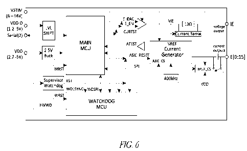
[0080] FIG. 6 schematically illustrates a block diagram of
a fail-safe hybrid system.
The system can have a first control unit, e.g., main microcontroller unit
(MCU) that is
configured to implement a charge management algorithm through a current
generator and an
IE voltage output. The system can also include a second MCU, e.g., a watchdog
MCU, also
referred to herein as a monitoring MCU, that can have an independent charge
management
algorithm that can monitor the main MCU and can shut the system down in the
event of a
discrepancy. The main and watchdog MCUs can be configured to monitor the
electrodes and
system in a variety of ways which can include, for example, any number of: (1)
monitoring
electrode voltages to protect against electrode degradation and failures and
electronic failures;
(2) IE current monitoring to protect against device failures in AC or DC
modes; and/or (3)
voltage waveform morphology analysis to protect against device failures.
During AC mode,
blocking capacitors can be switched in-line. The main and watchdog MCU can
cross-check
each other for proper orientation. The system can include a third MCU, e.g., a
supervisor
watchdog MCU that can prevent devices from being reset. In external non-
implanted variants,
only a clinician may be allowed to change batteries to avoid stim cycling
termination when the
electrodes are loaded with charge.
[0081] FIG. 7 shows a table of non-limiting potential
failure mechanisms listed in
rows and mitigation mechanisms in columns. A check mark indicates which
mitigations protect
against which failures, according to some embodiments. When failures occur,
stimulation is
stopped either immediately (instant off) or at the end of a stimulation cycle
when finishing in
a charged balance state is beneficial. For example, bias current monitor out
of range protects
from a surface electrode (IE) disconnection, a current source error, a
coupling capacitor error,
or instrumentation signal chain error resulting in instant off stimulation.
Cyclic VPP out of
range (e.g., 10 or other numbers of cycles) is a primary mechanism protecting
from long term
electrode degradation resulting in the stimulation being ended at the
completion of a stim cycle.
Waveform morphology violation (e.g., 10 or other numbers of cycles) protects
against
electrode disconnection, current source failure or an instrumentation error
resulting in the
stimulation cycle being ended and the completion of a stim cycle. MCU/WD
voltage
supervision protects against stimulation or other power supply issues and
terminates
-21-
CA 03220236 2023- 11- 23
WO 2022/251519
PCT/US2022/031162
stimulation immediately and possible power off. Hardware watchdog protection
protects
against firmware/MCU failures resulting in general reset and ending the stim
cycle
immediately. Offline impedance check
________________________________________________ precheck to exclude failed
electrode and insufficient
electrode capacity. MCU/WD cross check assures that both MCUs are operating
properly
resulting in general reset and ending the stim cycle immediately. Independent
charge
management algorithms (two different algorithms with independent code bases)
protect against
firmware bugs and unanticipated algorithm deficiencies, resulting in general
reset and ending
the stim cycle immediately.
[0082]
In some embodiments, a device can include a virtual ground configured
to
be operably connected to the indifferent electrode where the virtual ground
can be set to any
level to minimize power dissipation.
[0083]
In some embodiments, current used from the output multiplexers are
measured to detect any failures in the active silicon components that are tied
directly to the
body to prevent unintended DC currents due to part failures that occur
especially due to ESD
discharge damage.
[0084]
In some embodiments, a device comprises any number of the following
mitigation mechanisms: (a) indifferent electrode current monitoring halts
operation if the bias
currents deviate from a preset minimum and maximum range, the current used can
be
processed with a statistical process to remove noise; (b) Electrode Voltage
monitoring either
from each working electrode to the indifferent electrode, each working
electrode to a reference
electrode, or between a pair of working electrodes; (c) Electrode monitoring
is resolved either
instantaneously or statistically across a preset time from, for example, 1 vis
to 1 hour or more
or less, or synchronized to waveform transitions, statistics can include:
mean, median,
variance, minimum, and/or maximum; (d) Electrode monitoring can examine the
electrode
voltages in their entirety or break it into components using either a filter
mechanism or by
subtracting out components based upon what is known about the electrode, e.g.,
what is
measured or the specifications of the electrode. As one example, the
aforementioned above
filtered voltage ¨ stimulation current * measured access resistance can be
below a specified
value.
[0085]
FIG. 8 illustrates a graph relating to lost capacity¨which can be
related to
voltage protections. Cyclic VPP: VPP ¨ 2*RA*I, which can help ensure that peak
voltage over
-22-
CA 03220236 2023- 11- 23
WO 2022/251519
PCT/US2022/031162
a stimulation cycle stay within prescribed limits to assure an electrode has
sufficient capacity
over time. Electrode waveform morphology (sawtooth) can help ensure that the
electrode
voltage waveform is as expected for prescribed currents
_____________________________ which can help assure that the
system is operating properly.
[0086]
FIGS. 9A and 9B relate to bias current monitoring. FIG. 9A illustrates
a
graph relating to the disconnection of a reference electrode. FIG. 9B
illustrates a graph relating
to the bias current being removed. Bias current monitoring can protect against
various faults,
which can include IE failure (open circuit or Hi-Z), WE failure (open circuit
or Hi-Z), WE
current source failure (Hi or Low), TE voltage source failure (no current of
forces current source
into failure), and/or capacitor bypass switch failure (current leakage or fail
open). For DC
specific modulation modes, the monitor can check that the bias is in the
correct range (e.g.,
25-75 viA). For AC specific modulation modes, the monitor can check that DC
current is less
than a predetermined value, such as, for example, < 100 nA (e.g., electronic
or multiple
capacitor failures).
[0087]
FIG. 10 relates to reducing (e.g., minimizing) irrecoverable charge.
FIG.
illustrates stimulation startup against time in seconds. The injection of bias
current can
place the electrode into an operational voltage range that can allow the
charge and/or electrode
life to be increased, such as maximized. The operating condition of the
electrode can be
determined, which can include determining that the electrode is in good
operating condition.
It can be determined that the electrode is in good operating condition by, for
example: ( 1 )
determining (e.g., assuring) that the peak of the referenced voltage waveform
is below a
calculated or empirically calculated voltage, and/or (2) integrating the
voltage of a cycle as an
indicator of irreversible charge and/or determine (e.g., assure) that it is
under a specific
threshold.
[0088]
FIG. 11 illustrates an example block diagram relating to HW and FW fail-
safe. Charge management algorithms¨main MCU controls ASIC (or discrete current
generator). MCU/WD voltage/current supervision¨independent ADCs and algorithms
in
main and watchdog can be kept alive by Watchdog MCU assuring HW and FW are
operational.
MCU/WD cross check¨Main and Watchdog MCU check-up on each other to assure HW
and
FW are operational. MCU/WD ASIC reset¨either the main or watchdog MCU can
reset
ASIC when a problem is detected.
-23-
CA 03220236 2023- 11- 23
WO 2022/251519
PCT/US2022/031162
[0089] A block diagram of an example stimulation engine
(sometimes referred to
as a waveform generator or therapeutic waveform generator) that can provide DC
and AC
therapy, including simulation with a single architecture is illustrated in
FIG. 12. A
conventional approach for medical devices is to utilize only one
microprocessor to both control
generating stimulation on an electrode and to check the stimulation on the
electrode. Such
approaches render as therapeutic system susceptible to a double failure that
can result in patient
harm. From a safety standpoint, this results in all system software as having
a higher risk
classification (e.2., of higher risk class C instead of lower risk class A or
B). By providing an
independent microprocessor that monitors the electrode, such as shown in the
architecture of
FIG. 12, three simultaneous failures would need to occur to create a harmful
situation to a
patient. The independent safety microprocessor (e.g., the Safety MCU, as shown
in FIG. 12)
reduces overall risk and improves safety. This allows the safety
classification of the software
and the system to be reduced (e.g., from higher risk class C to lowest risk
class A). This greatly
simplifies the design and testing of the system, as well. The stimulation
engine can stimulate
with a single bipolar pair of current generators. The main micro controller
unit (MCU,
processor or controller) can generate stimulation waveforms and the safety MCU
can
continuously verify proper system operation. The Boost Converter and LDO (low
dropout
regulator) can set the low noise stimulation compliance voltage (VSTIM) to
drive Bipolar
Current Generators SRCA, SRCB. The current generators SRCA, SRCB can be
sufficiently
fast to support AC waveforms having 1, 5, 10, 15, 20, 25, 30, 35, 40, 45, 50,
55, 60, 65, 70,
75, 80, 85, 90, 95, or 100 i..ts rise and fall times. Driving voltage for such
generators (VSTIM)
is sufficiently high such that that the current generators operate within the
common mode input
range to preserve power.
[0090] During low duty cycle AC (e.g., tonic) stimulation,
VSTIM can be
substantially (e.g., mostly) set to zero volts¨shutting down the stimulation
engine to preserve
power. Since the system can operate from a single supply, the virtual ground
(VIE) can be set
to the mid-rail for AC. During DC (e.g., ULF), VIE can be set to a fraction of
VSTIM
dependent upon the bias voltage, created by the bias current, that develops
around the electrode
operating voltages to save power. Stimulation voltages and currents can swing
around VIE.
Since bias current moves voltages below the mid-rail, the VIE can be designed
to chase those
voltages to save power. For DC mode, VIE can absorb the constant offset
current and can be
-24-
CA 03220236 2023- 11- 23
WO 2022/251519
PCT/US2022/031162
connected to the indifferent electrode (IE) which can be a surface electrode
for the stimulation
engine and the can (e.g., housing or enclosure) for the stimulation engine.
During AC modes,
the charge imbalance that can collect on the inside of blocking capacitors
CBA, CBB due to
charge imbalance can be discharged onto the VIE. In AC mode, the indifferent
electrode IE is
disconnected from the patient. VIE can be further set either toward the VSTIM
or ground rail
when the electrode achieves a bias voltage to further optimize power.
[0091] Bipolar current generators SRCA, SRCB can push or
pull current to support
the required balanced or intentionally unbalanced bipolar simulation mode. For
example, the
generators SRCA, SRCB can operate in bipolar mode and can be configured to
deliver opposite
and equal or unequal currents. In AC mode, they can be configured to generate
equal and
opposite currents. In DC mode, they can be opposite, and may optionally
include slightly
offset currents. Since the matching requirements are very high (-1 1,1A)
separate trim DACs
(digital-to-analog converters) (TRIMA DAC, TRIMB DAC) for both currents are
employed.
Both DC offsets and AC zeroing can be accomplished by utilizing the trim DACs,
e.g., TRIMA
DAC, TRIMB DAC. For example, residual post-calibration non-linearities may
exist due to a
mismatch between the complementary pair of current generators. To address,
this one of the
current generators (e.g., SRCA) may be arbitrarily selected as a reference
source. A secondary
calibration may be performed to force the adaptive current generator (e.g.,
SRCB), to match
the reference source (e.g., SRCA). This calibration is applied to the TRIM DAC
(e.g., TRIMB
DAC) on the adaptive current generator (e.g., SRCB), which then matches the
differential non-
linearities, and allows the normal calibration to correct the overall non-
linearities (including
the differential non-linearities). In DC mode, source DACs SRCA DAC, SRCB DAC
can
deliver the slowly varying current and, as mentioned herein, the trim DACs can
trim the values
and set the offset. The source DACs SRCA DAC, SRCB DAC can be updated by
software
through the SPI port when the current value needs to change, but can change at
any rate, up to
100 Hz or more, or others, but during stimulation plateaus, a single
stimulation value can
persist for several seconds.
[0092] In AC mode, stimulation can vary quickly so the
cathodic (activation)
current amplitude can be programmed into one source DAC, e.g., SRCA DAC and
the recovery
amplitude can be programmed into the other source DAC, e.g., SRCB DAC before
the start of
stimulation or when stimulation is changed. AC pulses can be formed quickly
and with high
-25-
CA 03220236 2023- 11- 23
WO 2022/251519
PCT/US2022/031162
efficiency by flipping the source of each current source to be either one
source DAC, e.g.,
SRCA DAC, mid-supply (for zero current), or the other source DAC. e.g., SRCB
DAC.
[0093] Two blocking capacitors CBA, CBB can be used to
guarantee DC blocking
in AC mode but can be bypassed in DC Mode. Rebalances switches RBSWA, RBSWB
(also
referred to as DSW1, DSW2, REBALA, REBALB, D1, D2) can recover charge from the
blocking capacitors CBA, CBB and can be used for self-test and other
calibration modes.
Discharge switches RBSWA, RBSWB may be used to discharge blocking capacitors
CBA,
CBB. In one embodiment, the stimulation engine includes one or more switches,
e.g., ULFSW
that can close to bypass/short blocking capacitors CBA, CBB when operating in
DC (or ULF)
mode, but open to cause the driving current to pass through the blocking
capacitors CBA and
CBB when operating in AC mode. The driving current is then directed through
multiplexers
SRCA MUX, SRCB MUX and routed to a desired electrode E01-E16. During AC mode,
the
capacitors CBA, CBB may be used to assure that the current to the electrodes
E01-E16 is
balanced.
[0094] In one embodiment, blocking capacitors CBA, CBB are
located on the input
side of the multiplexers SRCA MUX, SRCB MUX. Such arrangement avoids the need
to place
a separate capacitor on each electrode E01-E16, which simplifies circuit
design and reduces
the footprint of the implantable stimulation engine. The multiplexers SRCA
MUX, SRCB
MUX advantageously allow significant customizability of the stimulation
engine. For
example, an implantable lead of the simulation engine may include 16
electrodes. The
multiplexers SRCA MUX, SRCB MUX allow the stimulation engine to be configured
to
deliver any desired electrical waveform to any desired electrode. Furthermore,
the
multiplexers SRCA MUX, SRCB MUX or other multiplexer, e.g., VRE, allows any of
the
electrodes to be selected to function as a reference electrode. With such
configurability, the
can, or indifferent electrode of the stimulation engine does not necessarily
need to be utilized
as the stimulation engine's reference electrode. Instead, any one of the
electrodes E01-E16
may be utilized as a reference electrode. Furthermore, each electrode may be
selected by a
multiplexer VRE, SRCA MUX, SRCB MUX, to operate as an anode or cathode of the
stimulation engine's tissue stimulation signal.
[0095] Also, during AC mode, the IE can be disconnected
through a fault tolerant
set of series IE switches IESW1, IESW2. The IE current sensor Tie can be used
for fault
-26-
CA 03220236 2023- 11- 23
WO 2022/251519
PCT/US2022/031162
detection and to measure a constant offset current in DC and can also be used
for self-test
calibration and diagnostic modes. Current steering diodes (not shown) can
protect all system
outputs against over-voltage on the terminals and the series configuration can
protect shorting
to ground from single point failures.
[0096] Electrocautery can present a significant challenge
to therapeutic waveform
generators, including SCS devices because it can source 200 W @ 1000 V @ 490
kHz.
Defibrillators present a similar challenge. These voltages can result in
damage to the driving
electronics, resulting in device malfunction and failure. This challenge is
amplified in devices
with distantly spaced electrodes, such as those with spacing between the
working and
indifferent, or return, electrodes. The indifferent and working electrodes can
be separated by a
large distance, resulting in a high potential difference between electrodes
that is fed into the
electronics. An example of such a configuration is one that that utilizes an
active can, where
the metal casing is an active component in the electrical circuit, where the
can is not placed
near the working electrodes. Another example includes configurations with
inactive cans,
where the can is not an active component in the electrical circuit, and an
alternate indifferent
or return electrode, including but not limited to a surface electrode,
separate implanted
electrode, or electrode contact on an electrode array, where the indifferent
or return electrode
is not near the working electrodes. Another example includes configurations
with locally
placed indifferent, or return, electrodes, including but not limited to
configurations in which
an electrode contact on an array is specified as a return or indifferent
electrode. In all of these
non-limiting examples, the spacing between working electrodes typically
presents less risk due
to the comparatively reduced separation distance to an indifferent, or return,
electrode.
However, these working electrodes present a non-zero risk for electrocautery
damage.
[0097] It is therefore desirable to include protection
mechanisms to safeguard
against electrocautery, defibrillator, or other high-voltage/high-current
damage. Some
therapeutic waveform generators and SCS systems utilize capacitors at the
electrodes to
provide protection against electrocautery damage. However, the requisite lack
of isolation
capacitors in low-frequency, ultra-low frequency, and DC systems at the
electrodes requires
an alternate approach that does not rely upon capacitors.
[0098] FIG. 13 illustrates one example of a system for
protecting against high
voltage and/or high current that utilizes current steering diodes and fast-
acting positive
-27-
CA 03220236 2023- 11- 23
WO 2022/251519
PCT/US2022/031162
temperature coefficient (PTC) devices. A Zener diode in series with two PTCs
connects an
electrode can to the driving electronics. In the presence of externally
applied voltages of
moderate magnitude, such as electrostatic discharge, the Zener diode clamps
the external
voltage to a safe level, such as 5, 10, 15, 20, 25, less than 25, or less than
30 V. Externally
applied voltages that result from electrocautery present high voltages that
would result in
irreversible breakdown of the Zener diode. Placing one or more PTC devices in
series with the
Zener diode safeguards the Zener diode from damage to disconnect the electrode
can from the
driving circuitry. High voltage/current will result in a temperature increase
across the PTC,
increase in PTC resistance, and a significant reduction in the power burden of
the Zener. FIG.
14 illustrates how this series configuration can enable voltage clamping to
¨18 V in the
presence of high-voltage electrocautery signals.
[0099] Referring back to FIG. 12, instrumentation of the
stimulation engine can
include measurement of the working electrode voltages VweA, VweB, the
indifferent electrode
voltages Vie, and the reference electrode voltage Vre where the reference
electrode is 1 of the
total number, e.g., 4, 16, etc., of selectable working electrodes. All of the
foregoing
instrumentation can be used for diagnostics, calibration, and/or to implement
safety and control
measures. All voltages can be buffered before routing into both the main and
safety MCU
ADCs where these independent MCUs can be used, at least in part, to achieve a
safe fault
tolerant system.
[0100] Four (or more or less) (e.g., E01, E08, E09, E16) of
the sixteen (or more or
less) working electrodes can be hardwired to the reference electrode
multiplexer VRE. One
(or more or less) of those electrodes can be selected electronically as a
reference and can be
placed into electrical communication with a VREF Amplifier (not shown) though
two series
resistors VR1, VR2 to limit the current to, e.g., < 5, 10, 15, 20, 25, 30, 35,
40, 45, or 50 p A in
the case of a worst-case amplifier failure. Reference electrode multiplexer
VRE can be
selected momentarily when sampling the reference voltage. A valid reference
voltage Vre
measurement can be made by any electrode that is not being used to stimulate
or otherwise
provide a therapeutic signal to a patient.
[0101] AC neurostimulation systems can rely primarily on
isolating active circuitry
from the body with series capacitors. In conjunction with internal discharge
resistors/switches
the capacitors not only protect from circuit failures but provide charge
balanced waveforms.
-28-
CA 03220236 2023- 11- 23
WO 2022/251519
PCT/US2022/031162
High-capacity electrode systems that utilize balanced or imbalanced charge
biphasic
waveforms that operate at ultra-low frequencies utilize DC stimulation and
cannot readily
utilize capacitors. As a result, alternate safety mechanisms must be
implemented. Similarly,
the same limitations may apply for systems that use balanced charge biphasic
waveforms (e.g.,
ULF waveforms on balanced systems). Therefore, alternative (non-capacitor-
based) solutions
may be utilized in such systems, as well.
[0102] In one embodiment, DC mode operates by providing an
imbalanced charge
ultra-low frequency imbalanced waveform that can operate the electrode within
its protective
voltage region where long term electrode capacity is optimized and preserved.
The safety
mechanisms can assure that resulting electrode voltages stay within the
prescribed range as
evaluated by at least two independent mechanisms, even in the case of one or
more system
fault, any detected faults can result in stimulation shutdown and power down
of the stimulation
engine.
[0103] To better understand such safety mechanisms, the
electrode can be
modelled by a simplified Randles Cell: a series access resistance (Ra) and
capacitance (Cdl)
and polarization resistor (Rp or Rct). The polarization resistor because it is
about >10x larger
than Ra will be ignored in this treatment. The total voltage across the
electrode (Vt) is equal to
Ra * I + Cyclic Vpp where Cyclic Vpp is the peak-to-peak voltage across the
capacitive
component (Cdl) of the electrode. Given this relationship, Va (from Ra x I)
and Cyclic Vpp
can be separated on each stimulation cycle using real-time measure of Vt and
being able to
calculate Ra.
[0104] To ensure tissue safety, operating electrodes within
their electrode
capacities can be important. Driving electrodes outside of their capacity
eventually may reduce
electrode capacity and facilitate reactions that may impact tissue health and
cause irreversible
electrochemical reactions. Cyclic Vpp is the primary measure of electrode
health and is
inversely proportional to the capacity of electrodes. Cyclic Vpp is expected
to be fairly
constant once the electrode has achieved steady state operation. If changes to
the electrode
over its life occur, these can be detected via Cyclic Vpp and stimulation can
be adjusted to
ensure operation within the electrode capacity, or the stimulation electrodes
may be changed
as needed.
-29-
CA 03220236 2023- 11- 23
WO 2022/251519
PCT/US2022/031162
[0105] In AC stimulation mode, blocking capacitors CBA, CBB
can be positioned
between the electrode contacts and the current outputs to protect against DC.
In DC
neuromodulation mode, e.g., stimulation mode, the capacitors CBA, CBB can be
disabled with
a switch ULFSW. A variety of failure modes may be realized with capacitors and
switches.
For example, there can be a failure mode such that if a capacitor CBA, CBB
fails, it can pass
DC to the indifferent electrode IE, and the DC current can be detected (e.g.,
by current sensor
Tie, etc.). There can be a failure mode such that if a capacitor fails, the
other capacitors can
protect the body from DC through the other electrodes. There can be a failure
mode such that
if a switch fails, DC can pass to the indifferent electrode that can be
detected. There can be a
failure mode such that if the current outputs in AC mode fail, capacitors can
protect the body
from DC. There can be a failure mode such that if the current outputs in DC
mode fail that
can be detected on the indifferent electrode.
[0106] The stimulation engine may include two processors: a
Main MCU and a
watchdog or Safety MCU. In DC mode, the Main MCU implements a charge
management
algorithm (CMA) using a current generator and an IE voltage output (virtual
ground). The
watchdog or Safety MCU can have an independent charge management algorithm
that
monitors the Main MCU and can shut the system down in the case of a
discrepancy. The Main
and Safety MCUs can monitor each other with an independent ADCs monitor:
electrode
voltages to protect against electrode degradation and failures and electronic
failures; IE
currents to protect against device failures and in appropriate DC levels;
and/or voltage
waveform morphology to protect against device failures. The Main and Safety
MCUs can
cross-check each other for proper operation. The Main and Safety MCUs can both
reset/disable the ASIC. There can be a variety of failure modes. For example,
if the charge
management algorithm fails in the Main MCU, the Main MCU may observe electrode
voltage
issues; the Main MCU may determine if IE current goes out of range; the Safety
MCU may
observe electrode voltage issues; and/or the Safety MCU may determine if IE
current goes out
of range. If the Main MCU malfunctions, the Safety MCU can observe such
condition and
request stimulation stop and then reset the Main MCU and ASIC and/or the
supervisor chip
can observe condition and force both Main and Safety MCU and ASIC into reset.
If the Safety
MCU malfunctions, the Main MCU can observe conditions and request stimulation
stop then
-30-
CA 03220236 2023- 11- 23
WO 2022/251519
PCT/US2022/031162
reset the Safety MCU and ASIC and/or the supervisor chip can observe condition
and force
both the main and Safety MCU and ASIC into reset.
[0107] In addition, the Main MCU can control the current
generator (e.g., using
TRIMA DAC & SRCA DAC that controls current source SRCA, SRCB DAC& TRIMB DAC
that controls current source SRCB and an IE voltage output (virtual ground)
(e.g., using VIE
DAC and amplifier DRV). The Safety MCU can have an independent charge
management
algorithm that can monitor the Main MCU and can shut the system down in the
case of a
discrepancy. The Main and Safety MCUs monitor each other, and each can include
an
independent ADC monitor: IE currents to protect against device failures and
inappropriate DC
levels. The Main and Safety MCUs can cross-check each other for proper
operation. The Main
and Safety MCUs can both reset/disable the ASIC. There can be a number of
failure modes,
which can include that capacitor (e.g., CBA, CBB) or capacitor bypass switch
(e.g., ULFSW)
failure can cause IE current flows.
[0108] The stimulation engine (e.g., the stimulation engine
of FIG. 12 or other
stimulation engine as described herein) may be implemented as an application
specific
integrated circuit (ASIC). As such, the stimulation engine could also include
more than two
bypassable blocking capacitors, e.g., one blocking capacitor for each
electrode, e.g., 16
capacitors if 16 electrodes were employed. The current output the ASIC can be
clocked by an
oscillator; receive and execute commands from the main MCU; and/or analog
differential
electrode voltages buffered by internal and then external amplifier. There can
be various
failure modes. If the current output ASIC current source, oscillator, and/or
amplifier fail, the
Main and Safety MCU can detect errors in IE currents and/or the Main and
Safety MCU can
detect errors in electrode voltages including: cyclic VPP, waveform
morphology, and/or
electrode voltage.
[0109] In one embodiment, an IE amplifier DRV of FIG. 14
can buffer a voltage
generated from VIE DAC commanded from an MCU to drive the indifferent
electrode 1E,
which is sometimes referred to as a virtual ground. In DC mode, the IE can
absorb a bias
current that protects the electrode. In AC mode, the IE current typically not
utilized. The
current sensor Tie can measure the current to the IE to test for various
failure modes. For
example, if the IE amplifier DRV fails, the current output may not accept
additional current
from the IE, causing the electrode voltages to error and be noted by the MCUs.
In DC mode,
-31-
CA 03220236 2023- 11- 23
WO 2022/251519
PCT/US2022/031162
if the current sensor lie fails out of range, the MCUs can shut down
stimulation. During AC
mode, the current sensor Tie can be periodically tested to avoid the double
fault case when the
AC current sensor Tie fails low and a capacitor switch e.g., ULFSW fails.
[0110] The stimulation engine systems disclosed herein can
differ from other
systems in various aspects. In one aspect, the systems disclosed herein can
use an ultra-low
frequency (ULF) stimulation waveform and a low current offset (-current
offset"), which may
be in the form of a constant current offset. The ULF waveform current
amplitude can be
adjusted for the individual patient to achieve efficacy. The low current
offset can be used to
bias the operating voltage of the working electrodes such that they operate at
an increased (e.g.,
maximum) long-term charge transfer potential.
[0111] ULF waveforms can be charge balanced over a
stimulation cycle (minus the
current offset) and preferably are stopped on the end of a cycle to avoid
adverse patient
perceptions as well as undesired, unperceived neuromodulation. Likewise, in
some cases the
ULF waveform has all smooth transitions (e.g., rounded edges, not a square
wave) between
waveform segments to minimize such adverse patient perceptions and undesired,
unperceived
neuromodulation. In a bipolar mode, a current offset can be introduced into
the system by
shifting the charge-balanced ULF waveforms each by a predetermined fraction,
e.g., 1/2 the
target current offset level, and the unbalanced portion of the waveform, the
current offset, can
removed through the indifferent electrode (IE).
[0112] A non-limiting example measurement of a DC (e.g.,
ULF) waveform
stimulating a DC lead in-vitro (e.g., generated by the stimulation engine, and
during the
simulation engine's DC mode of operation) is shown in FIG. 15. Bipolar
currents are generated
by sourcing current from SRCA and sinking current SRCB, and then alternatively
sourcing
from SRCB and sinking through SRCA to switch the polarity. Switching the
polarity at a
specific rate allows the generation of any of the frequencies or frequency
ranges described
herein with a stimulation amplitude of a magnitude of any stimulation
amplitude described
herein. In one embodiment, the bias of each electrode is any bias value
described herein, and
may be in the mA, A or nA range. Bias is generated by intentionally
mismatching the source
and sink currents between the current generators and may be set in a
particular polarity without
a frequency. If the bias current is constant and negative, then that may shift
magnitude of the
positive value of the ultra low frequency waveform. If the bias current is
constant and positive,
-32-
CA 03220236 2023- 11- 23
WO 2022/251519
PCT/US2022/031162
that may shift the magnitude of the negative value of the ultra low frequency
waveform. A
complex non-DC bias can also be introduced using this technique.
[0113] A non-limiting example of an AC waveform (e.g.,
generated by the
stimulation engine and during the stimulation engine's AC mode of operation)
is shown in
FIG. 16. Only the Iwe2 and Vwe2-Vie voltages of the bipolar pair SRCA, SRCB
are shown
for clarity. The amplitude of the waveform is any amplitude described herein,
and may be in
100, 500, 1000, 2000, 3000, 4000, 5000, 6000, 7000, 8000, 9000, or 10000 A or
any other
amplitude and the recovery pulse is a fraction of the amplitude, such as 1/2,
1/3, 1/4, 1/5, 1/6, 1/7,
1/8, 1/9, 1/10 or any other fraction of the amplitude. The recovery pulse is
lx, 2x, 3x, 4x, 5x,
6x, 7x, 8x, 9x, 10x or other multiple longer than the active pulse. The
stimulation engine can
drive a zero cut-rent between the activation and recovery pulse. After the
recovery pulse is
complete, the current sources maintain a near zero current for the remainder
of the pulse for
the time it takes to reach the period corresponding to the pulse frequency.
[0114] The stimulation engine can include several
mitigation mechanisms and can
be categorized into firmware-based Charge Management Algorithm (CMA)
Components that
are firmware based and Hardware Mitigation Mechanisms¨as summarized in the
tables
illustrated in FIGS. 7 and 17. Although many of the mitigation mechanisms are
described with
respect to systems that deliver a ULF current with a bias current, the same
mitigation
mechanisms may be used with systems that deliver a ULF current without a bias
current, as
well.
[0115] CMA Components can be implemented independently on
independent
multiple, e.g., Main and Safety MCUs. Two independent firmware images running
two
independent algorithms running on two independent processors can have a very
low
probability of failing within a finite time window.
[0116] The table in FIG. 17 lists several mitigation
mechanisms or fault detection
events. Each row in the table corresponds to a mitigation mechanism. The
columns in the
table correspond to a mitigation mechanism ID, a description of the mitigation
mechanism,
and comment relating to the mitigation mechanism. Any number (e.g., all or a
subset) of
mitigation elements disclosed herein can be included and/or excluded in
neuromodulation
engines depending on the desired clinical result. Furthermore, any one of the
mitigation
mechanisms, when detected by a controller or processor, can cause a system
response,
-33-
CA 03220236 2023- 11- 23
WO 2022/251519
PCT/US2022/031162
including, but not limited to, preventing operation of the stimulation engine,
removing the
Vstim signal, disconnecting the battery, etc. In addition, the mitigation
mechanisms or fault
conditions may be detected by hardware, software, and/or firmware of the
stimulation engine.
[0117] The stimulation engine may employ a variety of
safety mechanisms to
assure proper function and redundancy checking of system performance. For
example, the
CMS mechanism relates to providing two or more processors (e.g., Main MCU (M-
MCU),
Safety MCU (sometimes referred to as the Watchdog MCU or W-MCU)) that
independently
operate and monitor the performance of each other, including the operation of
the other
processor's charge management algorithm (CMA). Two processors also provide
redundancy
so the stimulation engine may continue operating upon the unlikely failure of
one of the
processors.
[0118] The IIE mechanism refers to providing current
monitoring to detect current
errors when operating in DC mode. TIE current errors may result from either a
SRCA, SRCB,
VIE failure, an interconnection error, or a short to supply or ground For
example, the
stimulation engine of FIG. 12 may include a current sensor lie, as described
in greater detail
herein.
[0119] The HBSC mechanism refers to monitoring an MCU
heartbeat signal and
sequence checking. If either the Main MCU or the Safety MCU fails to generate
a heartbeat
signal, or if its sequence includes an error, one or both MCUs are reset. A
heartbeat signal
indicates that the microprocessors (Main MCU and Safety MCU) are operating.
However,
even if operating, it is still possible for them to be desynchronized. A
heartbeat count provides
an additional safety measure to assure that both processors are running
extended periods of
time without undetected resets and to assure that they stay synchronized. Such
a configuration
may be used to detect unexpected independent MCU reset conditions (e.g.,
desynchronization,
etc.).
[0120] A VMIN monitor can indicate whether the VSTIM
(stimulating Voltage)
(e.g., as detected at a selected working electrode E01-E16) is at a desired
level. A VMIN signal
can indicate whether VSTIM exceeds or fails to achieve the desired level, or
whether it is
outside of a threshold difference with a desired level.
[0121] The VSTM mechanism refers to a Vstim or stimulating
voltage monitor.
Vstim may be generated by a boost converter, as shown in FIG. 12. Vstim may be
actively
-34-
CA 03220236 2023- 11- 23
WO 2022/251519
PCT/US2022/031162
regulated and monitored to assure that it does not exceed a maximum expected
voltage. This
protects against open circuits or degraded electrodes.
[0122] A VOSF monitor can indicate whether an over-current
fault has occurred.
For example, when the IVOS signal exceeds a threshold current level for more
than a specified
duration, a fault condition may be detected, and a system response (such as
those described
herein) may occur. The IVOS signal can correspond to a monitored current
signal from the
output power supply. The power supply current to a multiplexer is monitored,
as a current
exceeding an expected value can indicated multiplexer failure.
[0123] A VOVP mechanism refers to a VSTIM over voltage
protection
mechanism. This hardware mechanism shuts down the system to avoid circuitry
damage and
to avoid exposing the patient to undesired voltage levels.
[0124] The VPP mechanism refers to monitoring electrode
health, and is described
above with respect to FIG. 8. Other mechanisms to monitor electrode health and
performance
may be provided, as well. For example, real time monitoring of electrode
performance by
determining each electrode's series access resistance (Ra), capacitance (Cdl)
and polarization
resistance (Rp or Rct) can indicate whether the electrodes are operating as
anticipated. For
example, a change in electrode structure, plating, and/or position within the
subject can lead to
a change in one or more of such electrode parameters. Real time monitoring
provides an
indication when an undesirable change has occurred so that system operation
may be
suspended, or an electrode may be identified as possibly faulty. A faulty
electrode may then
be removed from the stimulation engine's output path by controlling a
multiplexer to avoid
selecting such electrode for stimulation output.
[0125] Examples of real-time measurement and calculation of
circuit parameters
are shown in Figures 18-21.
[0126] In some configurations, the series access
resistance, Ra, and double layer
capacitance, Cdl, can be measured using a test rectangular biphasic current
pulse and potential
measured between the working and indifferent electrode [Vwe-it(t)]. Rising and
falling edge
of the rectangular current waveform will correspond to voltage step, Vstep, in
the measured
potential as a result of the ohmic drop across the solution resistance (Ra),
with negligible
contribution from the electrode capacitance to the high-pass nature of the
capacitive interface.
Therefore, the voltage step produced by the current step of known magnitude I
will give Ra
-35-
CA 03220236 2023- 11- 23
WO 2022/251519 PCT/US2022/031162
from Ra = Vstep/I at the beginning and end of the biphasic pulse, and
Ra=abs(Vstep/(2*I)) from
during the polarity reversal. The capacitance can be determined from the
voltage increase,
Vplateau, from the rising to the falling edge time, toateau, of constant
current, I, due to the
approximately linear relationship between stored charge and voltage across the
electrode
interface. The voltage measurement will give Cdl from Cdl = Ptplateaui
Vplateau, or for some
portion of the plateau. In some configurations, this biphasic waveform can
consist of a single
biphasic pulse, or a series of biphasic pulses. In some configurations, this
biphasic waveform
can be applied prior to or at the cessation of delivery of the therapy
waveform to establish
initial and final values for Ra and Cdl. In some configurations, this biphasic
waveform can be
applied periodically during a pause in the delivery of the therapy waveform.
In some
configurations, this biphasic waveform can be applied between periods of the
therapy
waveform without pausing therapy using a very low current I and short period
and
subsequently small toateau to enable real-time assessment of electrode
parameters (FIG 18).
[0127] In some configurations, the series access resistance
Ra and cyclic peak-to-
peak voltage Vpp are approximated using a set of points sampled from the
potential measured
between the working and indifferent electrode [Vwe-te(t)] and the
instantaneous stimulus current
[1(O]. Sampled points are then analyzed using an algorithm to calculate Ra and
Vpp. Similar
analysis can be done between the working and reference electrodes [V,e,e(t)].
An example of
such a configuration is shown in FIG 19.
[0128] In one configuration, the algorithm includes the
following steps:
1. [0129] A time point, T2 is set at a current zero-crossing point.
2. [0130] A set of time points is bounded by time points Ti and T3, where
TI=T2 ¨ OT
and T3 = T3 6T, where 6T > 0.
3. [0131] Vwe-ie(t) is sampled at all time points bounded by Ti and T3
4. [0132] I(t) is sampled at all time points bounded by T3 and T3 from the
device
commands to output, or sampled from an output current monitor
5. [0133] A set of values for access resistance, Rest, is constructed from
entries R. for
Rmax> > Rama, where Rm., is an approximation for the minimum expected Ra, and
R. is an approximation for the maximum expected R..
6. [0134] A set of voltages V(t) is calculated for each entry in Rest as:
a. [0135] V(t) = {I Vwe-le(t) ¨ I(t) * r I: r E Rest, Ti < t < T3}
-36-
CA 03220236 2023- 11- 23
WO 2022/251519
PCT/US2022/031162
7. [0136] Find the local maximum for each set of voltages for each entry in
Rest
8. [0137] Set Ra equal to the element of Rest that generates the minimum local
maximum
9. [0138] Vpp can be calculated by the following equation, where T4is the
preceding
zero crossing point:
a. Vpp== IVwe-ie(T2) ¨ I(T2) * Ral - IVwe-ie(T4) ¨ I(T4) * Ral
[0139] In one configuration, the algorithm includes the
following steps:
1. [0140] Two time points. T5 and T2, are set at the most previous current
zero-
crossing and immediately preceding zero-crossing, respectively. Additional
time
points are set prior to and after each of these initial time points as a
function of a
sampling period T. In total, there will be 6 time points in the set: T = f Ti,
T2, T3,
T4, T5, T6 I, where T1=T2-Ts, T3=T2-FTs, T4=T5-Ts, and T6=T5+Ts.
2. [0141] Vwe_te(t) is sampled at each time point in the set, producing a
set of voltages:
V={ V1, V2, V3, V4, V5, V6}, where Vn=Vwe-ie(Tn)=
3. [0142] I(t) is sampled at each time point in the set from the device
commands to
output, or sampled from an output current monitor, producing a set of
currents:
I= II, 12, 13, 14, 15, , where In=I(T.).
4. [0143] A set of values for access resistance, Rest, is calculated using
the last known
value for Ra, Rao, and a delta value, oRa. The value Rao may come from an
estimate,
prestimulation measurement, or the last dynamic measurement, i.e. the previous
result of this algorithm. In total, there will be 3 resistance values in the
set: Rest =
{Rai, Ra2, Ra3}, where Rai = Rao ¨ ORa, and Ra3 = Rao + ORa.
5. [0144] Calculate a set of relative slopes in the sampled voltages
bounded by T3 and
Ti (or To and T4) for each resistor value as follows:
a. [0145] S=ll(V3-13*r) -(Vi-li*r)I: reRest)
6. [0146] Set Ra equal to the element of r that generates min{ S }. This
access
resistance will then be used in subsequent calculations and future
determinations
for Ra (setting Rao = Ra for the preceding algorithm)
7. [0147] Calculate the peak to peak voltage at the current zero-crossing
points as
follows:
a. [0148] Vpp = I V2 ¨ I2 * Ra I + I V5 ¨ I5 * Ra I
-37-
CA 03220236 2023-11-23
WO 2022/251519
PCT/US2022/031162
[0149]
In some configurations, the algorithm for a low frequency, biphasic
waveform includes the following steps:
1. [0150] A set of 8 time points is defined as follows across the biphasic
waveform:
a. [0151] To,6 = current zero-crossing time, where TO is from a previous
cycle and T6 is from the present cycle
b. [0152] T1,7 = beginning of first phase current plateau, where Ti is from
a previous cycle and T7 is from the present cycle
c. [0153] T2 = end of first phase current plateau
d. [0154] T3 = current zero-crossing time
e. [0155] T4 = beginning of second phase current plateau
f. [0156] Ts = end of second phase cut-rent plateau
2.
[0157] Vwe_ie(t) is sampled at each time point in the set, producing a
set of voltages:
V=1 Vo, Vi. V2, V3, V4, V5, V6, V7}, where Vn=Vwc-ic(Tn)=
3. [0158] I(t) is sampled at each time point in the set from the device
commands to
output, or sampled from an output current monitor, producing a set of
currents:
I={ Io, It, 12, 13, 14, 15, 16, 17 1, where In=I(Tn).
4. [0159] Cdl for the the first and second phase is determined from Cdl = Q /
(V3 ¨
V0) and Q / (V6 ¨ V3), respectively, where Q is known from the device commands
to output or from an output current monitor and the phase time.
5. [0160] Ra for the first and second phase is determined from Ra = (V2 ¨ V4)
/ -
14) and (V7 ¨ V5) / (17 ¨ 15)
6. [0161] Vcdl (Vpp elsewhere) for the first and second phase is determined
from
Vcdl = V3 ¨ VO and V6 - V3, respectively
[0162]
The previously described algorithms are capable of assessing Ra and
Vpp,
and thereby indirectly the capacitance of the working electrode, once every
half period. In
some configurations, it would be desirable to assess these parameters every
half period. In
some configurations, it may be desirable to assess these parameters less
frequently, such as
every 1, 1.5, 2, 2.5, 3, 3.5, 4, 4.5, 5, 5.5, 6, 6.5, 7, 7.5, 8, 8.5, 9, 9.5,
10, or greater periods. In
some configurations, it may be desirable to assess these parameters on demand
for evaluation
by an interested party, such as a patient, physician, device representative,
or other parties, or
at specific times, such as before device powers off, after device powers on,
and for some set
-3 8 -
CA 03220236 2023- 11- 23
WO 2022/251519
PCT/US2022/031162
period. In some configurations, it may be desirable to observe how these
parameters vary over
time, including over the total runtime, total implantation time, total number
of periods, or other
time windows of interest. In some configurations, this algorithm could be
applied in post-
processing, e.g., not in real-time, such as upon inspection by a device
programmer or physician.
[0163] In some configurations, it would be desirable to use
these measured
parameters to modify the delivered waveform. The following example illustrate
using such
parameters to modify the delivered waveform by the simulation engine or as a
safety
mechanism or mitigation mechanism to assure proper operation of the
stimulation engine.
[0164] Example 1 a: To assure that electrode is not used
over capacity control
current based upon real-time voltage across capacitor, that is limit current
so that Vcdl does
not increase beyond limit.
[0165] Example lb: To assure that electrode is used at
maximum capacity vary bias
to maximize Cdl.
[0166] Example lc: To assure maximum delivery of bipolar
currents use CDL of
each WE in pair and split bias between the two contacts to equalize the
contact capacity and at
a higher level sevro the total bias to achieve maximum combined CDL and
capacity.
[0167] Example 2a: Use real-time RA measure to get an
indication of surrounding
tissue health and limit current based upon this parameter.
[0168] Example 2b: Another option is to duty cycle current
over hours or days
assuming the tissue will recover. That rate may be due to profusion rate of
surrounding tissues.
[0169] Example 3: Modify waveform morphology (current
profile & duration) to
optimize charge and amplitude and bias to deliver efficacious stimulation with
the minimal
impact to the electrode and surround tissues by maximizing or minimizing CDL
and then using
RA as a tissue health indicator.
[0170] Each multiplexer (e.g., VRE, SRCA MUX, SRCB MUX,
etc.) of the
stimulation engine may be monitored, as well, to assure proper operation. For
example, VOS
(FIG. 12) may be monitored to check the current to and from each multiplexer.
Out of range
values (e.g., excessive current flowing to the power supplies of the
multiplexers) can indicate
a failure of one or more channels of (or the entire) multiplexer.
[0171] The WEMX mechanism refers to two multiplexers (e.g.,
SRCA MUX,
SRCB MUX of FIG. 12) are used to mitigate the risk of multiplexer failure, and
low level
-39-
CA 03220236 2023- 11- 23
WO 2022/251519
PCT/US2022/031162
ground leakages. By routing therapeutic current waveforms through two
multiplexers before
reaching a selected electrode (and patient), both multiplexers would need to
fail to cause low
level ground leakages.
[0172] The CBSW mechanism refers to utilizing capacitor
bypass switches
ULFSWA and ULFSWB to perform a self-test on the stimulation engine circuitry.
For
example, in one embodiment, the capacitor bypass switches ULFSWA or LTLFSWB
are
activated or deactivated while the multiplexers SRCA MUX, SRCB MUX short the
selected
working electrodes together to create a test loop. The stimulation engine then
tries to send a
DC signal through the test loop to determine if the capacitor bypass switches
and bypass
capacitors, and other circuits of the loop, are operating properly.
[0173] The MCU mechanism refers to providing redundant MCUs
(e.g., Main
MCU and Safety MCU), as discussed above. In some instances each MCU may
maintains
separate peripherals to improve reliability, or in some cases MCUs may share
peripherals or
share data from those peripherals.
[0174] The IESW mechanism refers to providing multiple
series switches to the
indifferent electrode. Such fault tolerance assures that the patient is not
exposed to the Vie
signal on the can during AC mode operation.
[0175] The VSR mechanism refers to providing multiple
series resistors to the Vref
signal. Such fault tolerance assures that in the extremely rare event of a
Vref failure resulting
in current flowing out of an input, the series resistors limit such current.
[0176] The VRMX mechanism refers to providing a separate
multiplexer VRE to
access and sense a reference voltage Vre on a selected electrode E01-E16. The
multiplexer is
configured to disconnect a Vref amplifier from the working electrodes (e.g.,
selected electrode
E01-E1 6) when it is not in use.
[0177] The BCAP mechanism, as described in additional
detail herein, refers to
dual blocking capacitors CBA, CBB (one for each amplifier SRCA. SRCB) that
guarantee that
the can may be switched into the stimulation path during AC stimulation mode
to assure that
no DC current is provided during the AC stimulation mode.
[0178] The ESD mechanism refer to the stimulation engine
including one or more
electrostatic discharge (ESD) pathways to sink unwanted electrostatic energy.
Each ESD
pathway may include a diode to the internal voltage rail and another diode to
the internal
-40-
CA 03220236 2023- 11- 23
WO 2022/251519
PCT/US2022/031162
ground rail. Where the voltage between the rails is limited by a clamping
diode of a selected
voltage. This configuration of diodes is referred to as steering diode
configuration and is
required to accommodate both bipolar and unipolar operation within a variable
voltage range
such that the parasitic diodes on the output circuits are protected where it
is assumed that the
operation voltages of those circuits is tied to the variable voltage range.
Each steering diode
can be converted to a series pair so if one diode fails the other will still
be operational. As a
further circuit optimization if multiple channels exist the 2nd series does
may be grouped
together into one diode device to reduce the component count.
[0179] The CALR mechanism refers to providing an
calibration load (e.g., CAL of
FIG. 12). The calibration load may be used in conjunction with the current
generators SRCA,
SRCB, TRIM-A, TRIM-B and the VIE current sense monitor to calibrate the
current
generators.
[0180] The WEAM mechanism refers to a WEAM monitor that
compares the
output voltages of the stimulation engines two amplifiers CSA, CSB. Because
the stimulation
engine operates in a bipolar state, a controller expects to see symmetrical
values (e.g., the
voltage of one amplifier should equal the same or opposite voltage of the
other amplifier), or
value that differ by only a small, known offset.
[0181] Furthermore, the ACALx mechanism refers to the
current outputs being
calibrated by switching in a calibration load CAL into the stimulation
engine's output path and
monitoring the current flowing through the calibration load (e.g., with a
current sensor lie). By
determining a difference between the measured current and the programmed or
desired current,
an offset or calibration adjustment may be made to the stimulation engine. For
example, the
input to a DAC may be increased or decreased by an offset value to compensate
for such
differences.
[0182] Double switches for redundancy on the capacitor CBA,
CBB bypass
switches ULFSW can provide an additional layer of security. Series switches
IESW1. IESW2
to the IE can also provide an additional layer of safety to protect against AC
transmission to
the stimulation engine's indifference electrode (e.g., metallic housing, or
can). Two high
impedance resistance resistors VR1, VR2 may be provided to protect against
unlikely amplifier
failure. A multiplexer VRE can be utilized to disable the electrode
multiplexers SRCA MUX,
SRCB MUX if a failure in the Vref system is detected. An amplifier calibration
load can be
-41 -
CA 03220236 2023- 11- 23
WO 2022/251519
PCT/US2022/031162
used to calibrate voltage amplifiers in conjunction with current generators.
For example,
amplifiers directing current to the IE should be accurately outputting the
desired currents.
When the stimulation engine is powered up, it can switch in a calibration
resistor to route
current into the calibration resistor, to the 1E, and to the current sensor
(Tie) to make sure that
the amplifier path is working properly. Such circuitry can also function as a
discharge path for
charge recovery. When in AC mode, two forms of charge recovery are possible.
During active
recovery, as discussed above, a pulse of a desired amplitude is output and
then a fractional
pulse is sent for a longer duration. For example, a 1 p.s stimulation pulse
may be delivered and
then an 8 p s recovery pulse may be applied. The same amount of current is
sent in opposite
directions. During passive recovery, a stimulation pulse is sent to the
electrode, and then a
capacitor or resistor is switched in to the circuit to recover.
[0183] FIG. 22 illustrates one embodiment of an output
multiplexer U20. The
multiplexer U20 may be used by the stimulation engine to select an electrode
to receive a
stimulation pulse, an electrode to form a return path for the stimulation
pulse, and/or an
electrode to serve as a reference electrode. The multiplexer U20 may be
employed as any one
or more of VRE, SRCA MUX, SRCB MUX, IESW1 and/or IESW2 of FIG. 12. In
addition,
the multiplexer U20 includes a back biasing diode D5 the prevents back biasing
to the
multiplexer. Back biasing could result in undesirable DC current flowing to
the multiplexer;
therefore, the back biasing diode D5 assures that the multiplexer U20 may not
enter into a state
in which it could possibly become back biased. The back biasing diode D5 may
be provided
with any one or more of the components VRE, SRCA MUX, SRCB MUX, IESW1 and/or
IESW2 of FIG. 12.
[0184] FIG. 23 illustrates various instrumentation
amplifiers U1A, U1B , U33A,
U33B, U3A, U3B, U5A, U5B, that may be used to measure the Vref, Vwe 1 , Vwe2
and IE
voltages of the stimulation engine. The voltages are read by one or more of
the Main MCU
and the Safety MCU of FIG. 12. Test points TP1-TP4 correspond to buffered Vre,
VweA,
VweB and Vie voltages.
[0185] FIG. 24 illustrates various current generators,
rebalance switches, trim
DACs, a polarity/zero circuit, and a current setting circuit. The current
setting circuit has two
DACs U7 and U8 (corresponding to SRCA DAC and SRCB DAC of FIG. 12). Each DAC
is
set to a different fixed output voltage level. The switch U21 (corresponding
to CFG of FIG.
-42-
CA 03220236 2023- 11- 23
WO 2022/251519
PCT/US2022/031162
12) of the polarity/zero circuit is able to quickly switch between the two DAC
outputs, and
sends the selected DAC output to the amplifiers U13A, U13B (corresponding to
SRCA and
SRCB of FIG. 12). The switch U21 is able to switch between the DAC outputs
much faster
than the DAC would be able to change its output in response to a changing
input. Therefore,
the switch U21 allows the stimulation engine to provide a very quick AC pulse
(e.g., 100 Hz,
250 i.ts pulse width, etc.). Two trim DACs U19, U6 (corresponding to TRIMB DAC
and
TRIMA DAC of FIG. 12) are able to trim the amplifiers in a variety of ways.
For example,
each trim DAC U19, U6 can be used to set a desired bias current to each
current source when
in ULF/DC mode. In addition, each trim DAC U19, U6 can also compensate for any
offset
voltages present in the op amps that are used to generate the currents (e.g.,
U13A, U13B).
Furthermore, rebalance switches U15A, U15B (con-esponding to RBSWA and RBSWB
of
FIG. 12) can be used to disconnect the IE from the can and use it as a virtual
ground to recover
charge off of the capacitors when in AC mode. In ULF/DC mode, the IE may be
used for the
bias current, which also serves as a virtual ground.
[0186] The stimulation engine of FIG. 12 includes an
indifferent electrode and
instrumentation to apply and control an active voltage on the stimulation
engine's indifferent
electrode. A digital-to-analog converter VIE DAC is controlled to generate an
indifferent
electrode voltage (or IE drive or virtual ground). The VIE DAC output passes
through a buffer
or voltage follower DRY. The stimulation engine can sense the current to the
indifferent
electrode with a current monitor lie. An amplifier may boost the voltage,
which is then
analyzed by one or both processors Main MCU, Safety MCU, to make sure that it
is in range.
[0187] FIG. 25 illustrates one embodiment of an adjustable
stimulation power
supply with fault detection employed by the stimulation engine of FIG. 12. The
illustrated
circuit may be used to sense the current used to drive the stimulation
engine's multiplexers. A
boost supply generates a high voltage signal Vboost for tissue stimulation.
The Vboost signal
is down regulated to generate a Vstim signal. Vboost is generated at a
switching regulator,
which can be noisy. Noise is lowered by adding the secondary regulator to
generate Vstim. A
DAC U2 is used to control the Vstim signal in order to optimize power. A fault
detector
(VSTIM Over Voltage Hard Fault) can determine if the Vstim signal has exceeded
the desired
level. If so, the fault detector turns off the Vstim signal. The mulitplexers
are supplied with
VOS+ and VOS- signals, and current is sensed at resistors R56, R57 and
amplified at current
-43-
CA 03220236 2023- 11- 23
WO 2022/251519
PCT/US2022/031162
sense amplifier U16. A comparator U32 can determine if the Vstim signal is too
high, or not
at the desired level. If so, a fault is sent to the microprocessor Main MCU,
Safety MCU. The
microprocessor can also be used to create a fault to test the fault detection
circuity. For
example, the microprocessor can set the regulator output very high to confirm
that fault
detection circuitry is operating correctly.
[0188] The foregoing description and examples has been set
forth to illustrate the
disclosure according to various embodiments and are not intended as being
unduly limiting.
The headings provided herein are for organizational purposes only and should
not be used to
limit embodiments. Each of the disclosed aspects and examples of the present
disclosure may
be considered individually or in combination with other aspects, examples, and
variations of
the disclosure. In addition, unless otherwise specified, none of the steps of
the methods of the
present disclosure are confined to any particular order of performance.
References cited herein
are incorporated by reference in their entirety.
[0189] While the methods and devices described herein may
be susceptible to
various modifications and alternative forms, specific examples thereof have
been shown in the
drawings and are herein described in detail. It should be understood, however,
that the
embodiments disclosed should cover modifications, equivalents, and
alternatives falling within
the spirit and scope of the various embodiments described herein and the
appended claims.
[0190] Depending on the embodiment, one or more acts,
events, or functions of
any of the algorithms, methods, or processes described herein can he performed
in a different
sequence, can be added, merged, or left out altogether (e.g., not all
described acts or events are
necessary for the practice of the algorithm). In some examples, acts or events
can be performed
concurrently, e.g., through multi-threaded processing, interrupt processing,
or multiple
processors or processor cores or on other parallel architectures, rather than
sequentially.
[0191] The use of sequential, or time-ordered language,
such as "then," "next,"
"after," "subsequently," and the like, unless specifically stated otherwise,
or otherwise
understood within the context as used, is generally intended to facilitate the
flow of the text
and is not intended to limit the sequence of operations performed.
[0192] The various illustrative logical blocks, modules,
processes, methods, and
algorithms described in connection with the embodiments disclosed herein can
be implemented
as electronic hardware, computer software, or combinations of both. To clearly
illustrate this
-44-
CA 03220236 2023- 11- 23
WO 2022/251519
PCT/US2022/031162
interchangeability of hardware and software, various illustrative components,
blocks, modules,
operations, and steps have been described above generally in terms of their
functionality.
Whether such functionality is implemented as hardware or software depends upon
the
particular application and design constraints imposed on the overall system.
The described
functionality can be implemented in varying ways for each particular
application, but such
implementation decisions should not be interpreted as causing a departure from
the scope of
the disclosure.
[0193] The various illustrative logical blocks and modules
described in connection
with the embodiments disclosed herein can be implemented or performed by a
machine, such
as a processor, a digital signal processor (DSP), an application specific
integrated circuit
(ASIC), a field programmable gate array (FPGA) or other programmable logic
device, discrete
gate or transistor logic, discrete hardware components, or any combination
thereof designed to
perform the functions described herein. A processor can be a microprocessor,
but in the
alternative, the processor can be a controller, microcontroller, or state
machine, combinations
of the same, or the like. A processor can also be implemented as a combination
of computing
devices, e.g., a combination of a DSP and a microprocessor, a plurality of
microprocessors,
one or more microprocessors in conjunction with a DSP core, or any other such
configuration.
[0194] The blocks, operations, or steps of a method,
process, or algorithm
described in connection with the embodiments disclosed herein can be embodied
directly in
hardware, in a software module executed by a processor, or in a combination of
the two. A
software module can reside in RAM memory, flash memory, ROM memory, EPROM
memory, EEPROM memory, registers, hard disk, a removable disk, an optical disc
(e.g., CD-
ROM or DVD), or any other form of volatile or non-volatile computer-readable
storage
medium known in the art. A storage medium can be coupled to the processor such
that the
processor can read information from, and write information to, the storage
medium. In the
alternative, the storage medium can be integral to the processor. The
processor and the storage
medium can reside in an ASIC. The ASIC can reside in a user terminal. In the
alternative, the
processor and the storage medium can reside as discrete components in a user
terminal.
[0195] Conditional language used herein, such as, among
others, -can,- "might,"
"may," "e.g.," and the like, unless specifically stated otherwise, or
otherwise understood within
the context as used, is generally intended to convey that some examples
include, while other
-45-
CA 03220236 2023- 11- 23
WO 2022/251519
PCT/US2022/031162
examples do not include, certain features, elements, and/or states. Thus, such
conditional
language is not generally intended to imply that features, elements, blocks,
and/or states are in
any way required for one or more examples or that one or more examples
necessarily include
logic for deciding, with or without author input or prompting, whether these
features, elements
and/or states are included or are to be performed in any particular
embodiment.
[0196] The methods disclosed herein may include certain
actions taken by a
practitioner; however, the methods can also include any third-party
instruction of those actions,
either expressly or by implication. For example, actions such as "positioning
an electrode"
include "instructing positioning of an electrode."
[0197] The ranges disclosed herein also encompass any and
all overlap, sub-ranges,
and combinations thereof. Language such as "up to," "at least," "greater
than," "less than,"
"between," and the like includes the number recited. Numbers preceded by a
term such as
-about" or -approximately" include the recited numbers and should be
interpreted based on
the circumstances (e.g., as accurate as reasonably possible under the
circumstances, for
example 5%, 10%, 15%, etc.). For example, "about 1 hour" includes "1 hour."
Phrases
preceded by a term such as "substantially" include the recited phrase and
should be interpreted
based on the circumstances (e.g., as much as reasonably possible under the
circumstances). For
example, "substantially perpendicular" includes "perpendicular." Unless stated
otherwise, all
measurements are at standard conditions including temperature and pressure.
The phrase "at
least one of' is intended to require at least one item from the subsequent
listing, not one type
of each item from each item in the subsequent listing. For example, -at least
one of A, B, and
C- can include A, B, C, A and B, A and C, B and C, or A, B, and C.
-46-
CA 03220236 2023- 11- 23