Note: Descriptions are shown in the official language in which they were submitted.
Attorney Docket No. P12714CA00
DESCRIPTION
TITLE OF INVENTION
OPTICAL DEVICE
TECHNICAL FIELD
[0001]
An embodiment of the present invention relates to an optical device, in
particular, an optical device using liquid crystal.
BACKGROUND ART
[0002]
An optical element which is a so-called liquid crystal lens has been
conventionally known in which a change in the refractive index of a liquid
crystal
is utilized by adjusting a voltage applied to the liquid crystal (for example,
see
Patent Literature 1, Patent Literature 2, or Patent Literature 3). For
example, the
lighting devices disclosed in the Patent Literature 1 and the Patent
Literature 2 use
a liquid crystal lens to distribute light from a light source in a circular
shape.
Further, the beam shaping device disclosed in the Patent Literature 3 changes
the
distribution shape of light by changing patterns of an electrode applied to a
liquid
crystal.
CITATION LIST
PATENT LITERATURE
[0003]
Patent Literature 1: Japanese laid-open patent publication No. 2005-
317879
CA 03222617 2023- 12- 13 1 / 36
Attorney Docket No. P12714CA00
Patent Literature 2: Japanese laid-open patent publication No. 2010-
230887
Patent Literature 3: Japanese laid-open patent publication No. 2014-
160277
SUMMARY OF INVENTION
TECHNICAL PROBLEM
[0004]
In an optical device using a liquid crystal, a light distribution may be
controlled by changing the magnitude of a voltage applied to the liquid
crystal. In
this case, the optical device requires the inclusion of a digital-to-analog
conversion
circuit (DAC) or an amplification circuit (AMP), which complicates control of
a light
distribution and causes an increase in manufacturing costs.
[0005]
In view of the above problem, one object of an embodiment of the present
invention is to provide an optical device with reduced manufacturing costs.
SOLUTION TO PROBLEM
[0006]
An optical device according to an embodiment of the present invention
includes an optical element including at least one liquid crystal cell
configured to
distribute light emitted from a light source, a power supply part configured
to
generate a first potential and a second potential different from the first
potential, a
control signal generation circuit part configured to generate a control signal
that
controls a pulse width of each of the first potential and the second
potential, and a
switch circuit part configured to output a first potential signal including
the first
potential with a first pulse width and the second potential with a second
pulse width
based on the control signal. The at least one liquid crystal cell includes a
first
CA 03222617 2023- 12- 13 2 / 36
Attorney Docket No. P12714CA00
substrate on which a first transparent electrode and a second transparent
electrode are alternately arranged in a first direction, and a second
substrate on
which a third transparent electrode and a fourth transparent electrode are
alternately arranged in a second direction intersecting the first direction.
The first
potential signal is input to the first transparent electrode.
[0007]
Further, an optical device according to an embodiment of the present
invention includes an optical element comprising at least one liquid crystal
cell
configured to distribute light emitted from a light source, a power supply
part
including a first power source configured to generate a first potential and a
second
power source configured to generate a second potential different from the
first
potential, a control signal generation circuit part configured to generate a
first
control signal, a second control signal, a third control signal, and a fourth
control
signal controlling a pulse width of each of the first potential and the second
potential, and a switch circuit part including a first switch circuit, a
second switch
circuit, a third switch circuit, and a fourth switch circuit. Each of the
first switch
circuit, the second switch circuit, the third switch circuit, and the fourth
switch
circuit electrically connected to the first power source and the second power
source. The first switch circuit outputs a first potential signal based on the
first
control signal, the second switch circuit outputs a second potential signal
based
on the second control signal, the third switch circuit outputs a third
potential signal
based on the third control signal, and the fourth switch circuit outputs a
fourth
potential signal based on the fourth control signal. The at least one liquid
crystal
cell includes a first substrate on which a first transparent electrode and a
second
transparent electrode are alternately arranged in a first direction, and a
second
substrate on which a third transparent electrode and a fourth transparent
electrode
are alternately arranged in a second direction intersecting the first
direction. The
first transparent electrode, the second transparent electrode, the third
transparent
CA 03222617 2023- 12- 13 3 / 36
Attorney Docket No. P12714CA00
electrode, and the fourth transparent electrode are electrically connected to
the
first switch circuit, the second switch circuit, the third switch circuit, and
the fourth
switch circuit, respectively. The first potential signal, the second potential
signal,
the third potential signal, and the fourth potential signal are input to the
first
transparent electrode, the second transparent electrode, the third transparent
electrode, and the fourth transparent electrode, respectively.
BRIEF DESCRIPTION OF DRAWINGS
[0008]
FIG. 1A is a schematic perspective view of an optical device according to
an embodiment of the present invention.
FIG. 1B is a diagram illustrating an optical device according to an
embodiment of the present invention.
FIG. 2 is a schematic perspective view of an optical element of an optical
device according to an embodiment of the present invention.
FIG. 3A is a schematic cross-sectional view of an optical element of an
optical device according to an embodiment of the present invention.
FIG. 3B is a schematic cross-sectional view of an optical element of an
optical device according to an embodiment of the present invention.
FIG. 4A is a schematic cross-sectional view illustrating control of a light
distribution by an optical element of an optical device according to an
embodiment
of the present invention.
FIG. 4B is a schematic cross-sectional view illustrating control of a light
distribution by an optical element of an optical device according to an
embodiment
of the present invention.
FIG. 5 is a schematic diagram illustrating connections between transparent
electrodes of an optical element and a switch circuit part in an optical
device
according to an embodiment of the present invention.
CA 03222617 2023- 12- 13 4 / 36
Attorney Docket No. P12714CA00
FIG. 6 is a circuit diagram showing a switch circuit included in a switch
circuit part in an optical device according to an embodiment of the present
invention.
FIG. 7A is a timing chart illustrating a relationship between control signals
input to a switch circuit part and a potential signal output from the switch
circuit
part in an optical device according to an embodiment of the present invention.
FIG. 7B is a timing chart illustrating a relationship between control signals
input to a switch circuit part and a potential signal output from the switch
circuit
part in an optical device according to an embodiment of the present invention.
FIG. 8 is a timing chart showing a relationship between potential signals
and a potential difference between transparent electrodes in an optical device
according to an embodiment of the present invention.
FIG. 9 is a timing chart showing a relationship between potential signals
and a potential difference between transparent electrodes in an optical device
according to an embodiment of the present invention.
FIG. 10 is a timing chart showing a relationship between potential signals
and a potential difference between transparent electrodes in an optical device
according to an embodiment of the present invention.
FIG. 11 is a graph showing a light distribution state using an optical device
according to an embodiment of the present invention.
DESCRIPTION OF EMBODIMENTS
[0009]
Hereinafter, each of the embodiments of the present invention is described
with reference to the drawings. However,
the present invention can be
implemented in various modes without departing from the gist of the invention
and
should not be interpreted as being limited to the description of the
embodiments
exemplified below.
CA 03222617 2023- 12- 13 5 / 36
Attorney Docket No. P12714CA00
[0010]
Although the drawings may be schematically represented in terms of width,
thickness, shape, and the like of each part as compared with their actual mode
in
order to make explanation clearer, they are only an example and an
interpretation
of the present invention is not limited. In addition, in the drawings, the
same
reference numerals are provided to the same elements as those described
previously with reference to preceding figures and repeated explanations may
be
omitted accordingly.
[0011]
In the case when a single film is processed to form a plurality of structural
bodies, each structural body may have different functions and roles, and the
bases
formed beneath each structural body may also be different. However, the
plurality of structural bodies is derived from films formed in the same layer
by the
same process and have the same material. Therefore, the plurality of these
films
is defined as existing in the same layer.
[0012]
When expressing a mode in which another structure is arranged over a
certain structure, in the case where it is simply described as "over", unless
otherwise noted, a case where another structure is arranged directly over a
certain
structure as if in contact with that structure, and a case where another
structure is
arranged via another structure over a certain structure, are both included.
[0013]
An optical device 1 according to an embodiment of the present invention
is described with reference to FIGS. 1A to 11. First, a configuration of the
optical
device 1 is described with reference to FIGS. 1A and 1B.
[0014]
[1. Configuration of Optical Device 1]
FIG. 1A is a schematic perspective view of the optical device 1 according
CA 03222617 2023- 12- 13 6 / 36
Attorney Docket No. P12714CA00
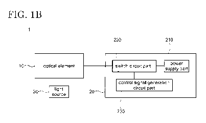
to an embodiment of the present invention. Further, FIG. 1B is a block diagram
illustrating the optical device 1 according to an embodiment of the present
invention. As shown in FIG. 1A, the optical device 1 includes an optical
element
and a control unit 20 that controls the optical element 10. Further, the
optical
5 device 1 may include not only the optical element 10 and the control unit
20 but
also a light source 30 that irradiates the optical element 10 with light. The
light
emitted from the light source 30 passes through the optical element 10 and is
emitted. The control unit 20 controls the optical element 10 to diffuse or
converge
the light passing through the optical element 10. That is, the optical device
1 can
10 control a light distribution.
[0015]
As shown in FIG. 1B, the control unit 20 includes a power supply part 210,
a switch circuit part 220, and a control signal generation circuit part 230.
The
optical element 10 is connected to a switch circuit part 220. Further, the
switch
circuit part 220 is connected to the power supply part 210. That is, the
optical
element 10 is connected to the power supply part 210 via the switch circuit
part
220.
[0016]
The power supply part 210 includes a power source that generates a
predetermined potential. For example, although the power supply part 210 may
include two power sources that generate two potentials, the power supply part
210
is not limited thereto. Further, the power supply part 210 may include a
potential
that is GND (e.g., 0 V). In addition, for convenience of explanation, even in
the
case of GND, it may be described as a power source that generates a potential
in
the present specification.
[0017]
The control signal generation circuit part 230 generates a control signal to
control the switch circuit part 220. A plurality of control signals for
controlling the
CA 03222617 2023- 12- 13 7 / 36
Attorney Docket No. P12714CA00
switch circuit part 220 may be generated. A switch circuit included in the
switch
circuit part 220 is a so-called analog switch. That is, the switch circuit
part 220
can control the supply of the potential generated by the power supply part 210
to
the optical element 10 based on the control signal from the control signal
generation circuit part 230. In the optical device 1, since the supply of the
potential generated by the power supply part 210 is directly controlled using
the
switch circuit part 220, the optical device 1 does not require a DAC or an
AMP.
[0018]
The control signal generation circuit part 230 is a computer that can
perform arithmetic processing using data or information. The control signal
generation circuit part 230 includes, for example, a central processing unit
(CPU),
a micro processing unit (MPU), a graphic processing unit (GPU), a field
programmable gate array (FPGA), a random access memory (RAM), or a dynamic
random access memory (DRAM). The control signal generation circuit part 230
can generate a control signal according to predetermined information (pulse
width
or duty ratio, etc.).
[0019]
Next, a configuration of the optical element 10 is described with reference
to FIGS. 2 to 3B.
[0020]
[2. Configuration of Optical Element 10]
FIG. 2 is a schematic perspective view of the optical element 10 of the
optical device 1 according to an embodiment of the present invention. As shown
in FIG. 2, the optical element 10 includes a first liquid crystal cell 110-1,
a second
liquid crystal cell 110-2, a third liquid crystal cell 110-3, and a fourth
liquid crystal
cell 110-4. The first liquid crystal cell 110-1, the second liquid crystal
cell 110-2,
the third liquid crystal cell 110-3, and the fourth liquid crystal cell 110-4
are stacked
in a z-axis direction. The second liquid crystal cell 110-2 is provided on the
first
CA 03222617 2023- 12- 13 8 / 36
Attorney Docket No. P12714CA00
liquid crystal cell 110-1. The third liquid crystal cell 110-3 is provided on
the
second liquid crystal cell 110-2. The fourth liquid crystal cell 110-4 is
provided on
the third liquid crystal cell 110-3. Although not shown in the figures, a
light source
is placed below the first liquid crystal cell 110-1. Therefore, light emitted
from the
light source 30 passes through the first liquid crystal cell 110-1, the second
liquid
crystal cell 110-2, the third liquid crystal cell 110-3, and the fourth liquid
crystal cell
110-4 in this order.
[0021]
The first optical elastic resin layer 1 70-1 adheres and fixes the first
liquid
crystal cell 110-1 and the second liquid crystal cell 110-2. The second
optical
elastic resin layer 170-2 adheres and fixes the second liquid crystal cell 110-
2 and
the third liquid crystal cell 110-3. The third optical elastic resin layer 170-
3
adheres and fixes the third liquid crystal cell 110-3 and the fourth liquid
crystal cell
110-4. An adhesive including a transparent acrylic resin or epoxy resin can be
used as each of the first optical elastic resin layer 170-1, the second
optical elastic
resin layer 170-2, and the third optical elastic resin layer 170-3.
[0022]
FIGS. 3A and 3B are schematic cross-sectional views of the optical
element 10 of the optical device 1 according to an embodiment of the present
invention. Specifically, FIG. 3A is a schematic cross-sectional view in a zx
plane
cut along a line A1-A2 shown in FIG. 2, and FIG. 3B is a schematic cross-
sectional
view in a yz plane cut along a line B1-B2 shown in FIG. 2. In addition,
hereinafter,
an x-axis direction and a y-axis direction may be described as a first
direction and
a second direction, respectively.
[0023]
The first liquid crystal cell 110-1 includes a first substrate 120-1 on which
a first transparent electrode 130-1 and a second transparent electrode 130-2
are
formed and a second substrate 120-2 on which a third transparent electrode 130-
CA 03222617 2023- 12- 13 9 / 36
Attorney Docket No. P12714CA00
3 and a fourth transparent electrode 130-4 are formed. A first alignment film
140-
1 is formed over the first substrate 120-1 in order to cover the first
transparent
electrode 130-1 and the second transparent electrode 130-2. Further, a second
alignment film 140-2 is formed over the second substrate 120-2 in order to
cover
the third transparent electrode 130-3 and the fourth transparent electrode 130-
4.
The first substrate 120-1 and the second substrate 120-2 are arranged so that
the
first transparent electrode 130-1 and the second transparent electrode 130-2
on
the first substrate 120-1 and the third transparent electrode 130-3 and the
fourth
transparent electrode 130-4 on the second substrate 120-2 face each other in a
crosswise manner (hereinafter, the same configuration is applied). Further, a
first
sealing member 150-1 is formed around each of the first substrate 120-1 and
the
second substrate 120-2. That is, the first substrate 120-1 and the second
substrate 120-2 are bonded to each other via the first sealing member 150-1.
Further, a liquid crystal is sealed in a space surrounded by the first
substrate 120-
1 (more specifically, the first alignment film 140-1), the second substrate
120-2
(more specifically, the second alignment film 140-2), and the first sealing
member
150-1 to form a first liquid crystal layer 160-1.
[0024]
The second liquid crystal cell 110-2 includes a third substrate 120-3 on
which a fifth transparent electrode 130-5 and a sixth transparent electrode
130-6
are formed and a fourth substrate 120-4 on which a seventh transparent
electrode
130-7 and an eighth transparent electrode 130-8 are formed. A third alignment
film 140-3 is formed on the third substrate 120-3 in order to cover the fifth
transparent electrode 130-5 and the sixth transparent electrode 130-6.
Further,
a fourth alignment film 140-4 is formed on the fourth substrate 120-4 in order
to
cover the seventh transparent electrode 130-7 and the eighth transparent
electrode 130-8. The third substrate 120-3 and the fourth substrate 120-4 are
arranged so that the fifth transparent electrode 130-5 and the sixth
transparent
CA 03222617 2023- 12- 13 10 / 36
Attorney Docket No. P12714CA00
electrode 130-6 on the third substrate 120-3 and the seventh transparent
electrode
130-7 and the eighth transparent electrode 130-8 on the fourth substrate 120-4
face each other. Further, a second sealing member 150-2 is formed around each
of the third substrate 120-3 and the fourth substrate 120-4. That is, the
third
substrate 120-3 and the fourth substrate 120-4 are bonded to each other via
the
second sealing member 150-2. Further, a liquid crystal is sealed in a space
surrounded by the third substrate 120-3 (more specifically, the third
alignment film
140-3), the fourth substrate 120-4 (more specifically, the fourth alignment
film 140-
4), and the second sealing member 150-2 to form a second liquid crystal layer
160-2.
[0025]
The third liquid crystal cell 110-3 includes a fifth substrate 120-5 on which
a ninth transparent electrode 130-9 and a tenth transparent electrode 130-10
are
formed and a sixth substrate 120-6 on which an eleventh transparent electrode
130-11 and a twelfth transparent electrode 130-12 are formed. A fifth
alignment
film 140-5 is formed on the fifth substrate 120-5 in order to cover the ninth
transparent electrode 130-9 and the tenth transparent electrode 130-10.
Further,
a sixth alignment film 140-6 is formed on the sixth substrate 120-6 in order
to cover
the eleventh transparent electrode 130-11 and the twelfth transparent
electrode
130-12. The fifth substrate 120-5 and the sixth substrate 120-6 are arranged
so
that the ninth transparent electrode 130-9 and the tenth transparent electrode
130-
10 on the fifth substrate 120-5 and the eleventh transparent electrode 130-11
and
the twelfth transparent electrode 130-12 on the sixth substrate 120-6 face
each
other. Further, a third sealing member 150-3 is formed around each of the
fifth
substrate 120-5 and the sixth substrate 120-6. That is, the fifth substrate
120-5
and the sixth substrate 120-6 are bonded to each other via the third sealing
member 150-3. Further, a liquid crystal is sealed in a space surrounded by the
fifth substrate 120-5 (more specifically, the fifth alignment film 140-5), the
sixth
CA 03222617 2023- 12- 13 11 / 36
Attorney Docket No. P12714CA00
substrate 120-6 (more specifically, the sixth alignment film 140-6), and the
third
sealing member 150-3 to form a third liquid crystal layer 160-3.
[0026]
The fourth liquid crystal cell 110-4 includes a seventh substrate 120-7 on
which a thirteenth transparent electrode 130-13 and a fourteenth transparent
electrode 130-14 are formed and an eighth substrate 120-8 on which a fifteenth
transparent electrode 130-15 and a sixteenth transparent electrode 130-16 are
formed. A seventh alignment film 140-7 is formed on the seventh substrate 120-
7 in order to cover the thirteenth transparent electrode 130-13 and the
fourteenth
transparent electrode 130-14. Further, an eighth alignment film 140-8 is
formed
on the eighth substrate 120-8 in order to cover the fifteenth transparent
electrode
130-15 and the sixteenth transparent electrode 130-16. The seventh substrate
120-7 and the eighth substrate 120-8 are arranged so that the thirteenth
transparent electrode 130-13 and the fourteenth transparent electrode 130-14
on
the seventh substrate 120-7 and the fifteenth transparent electrode 130-15 and
the sixteenth transparent electrode 130-16 on the eighth substrate 120-8 face
each other. Further, a fourth sealing member 150-4 is formed around each of
the
seventh substrate 120-7 and the eighth substrate 120-8. That is, the seventh
substrate 120-7 and the eighth substrate 120-8 are bonded to each other via
the
fourth sealing member 150-4. Further, a liquid crystal is sealed in a space
surrounded by the seventh substrate 120-7 (more specifically, the seventh
alignment film 140-7), the eighth substrate 120-8 (more specifically, the
eighth
alignment film 140-8), and the fourth sealing member 150-4 to form a fourth
liquid
crystal layer 160-4.
[0027]
The first liquid crystal cell 110-1, the second liquid crystal cell 110-2, the
third liquid crystal cell 110-3, and the fourth liquid crystal cell 110-4 have
the same
basic configuration. Therefore, in the following description, an arrangement
of
CA 03222617 2023- 12- 13 12 / 36
Attorney Docket No. P12714CA00
the transparent electrodes 130 of the first liquid crystal cell 110-1 is
described, and
the description of an arrangement of the transparent electrodes 130 of the
second
liquid crystal cell 110-2, the third liquid crystal cell 110-3, and the fourth
liquid
crystal cell 110-4 is omitted.
[0028]
In the first liquid crystal cell 110-1, the first transparent electrode 130-1
and
the second transparent electrode 130-2 extend in the y-axis direction, and the
third
transparent electrode 130-3 and the fourth transparent electrode 130-4 extend
in
the x-axis direction. Further, the first transparent electrode 130-1 and the
second
transparent electrode 130-2 are arranged alternately in a comb-teeth shape in
the
x-axis direction, and the third transparent electrode 130-3 and the fourth
transparent electrode 130-4 are alternately arranged in a comb-teeth shape in
the
second direction. In a plan view, although the extending
direction (y-axis
direction) of the first transparent electrode 130-1 and the second transparent
electrode 130-2 is orthogonal to the extending direction (x-axis direction) of
the
third transparent electrode 130-3 and the fourth transparent electrode 130-4,
they
may intersect each other with a slight shift from the orthogonal direction.
[0029]
In the plan view, the first transparent electrode 130-1 of the first liquid
crystal cell 110-1, the fifth transparent electrode 130-5 of the second liquid
crystal
cell 110-2, the ninth transparent electrode 130-9 of the third liquid crystal
cell 110-
3, and the thirteenth transparent electrode 130-13 of the fourth liquid
crystal cell
110-4 overlap each other so that their extending directions (y-axis direction)
substantially match each other. However, the first liquid crystal cell 110-1
to the
fourth liquid crystal cell 110-4 may be arranged so that the first transparent
electrode 130-1, the fifth transparent electrode 130-5, the nineth transparent
electrode 130-9, and the thirteenth transparent electrode 130-13 overlap each
other with a slight shift.
CA 03222617 2023- 12- 13 13 / 36
Attorney Docket No. P12714CA00
[0030]
For example, a rigid substrate having light-transmitting properties such as
a glass substrate, a quartz substrate, or a sapphire substrate is used as each
of
the first substrate 120-1 to the eighth substrate 120-8.
Further, a flexible
substrate having light-transmitting properties such as a polyimide resin
substrate,
an acrylic resin substrate, a siloxane resin substrate, or a fluorine resin
substrate
can also be used as each of the first substrate 120-1 to the eighth substrate
120-
8.
[0031]
Each of the first transparent electrode 130-1 to the sixteenth transparent
electrode 130-16 functions as an electrode for forming an electric field in
the liquid
crystal layer 160. For example, a transparent conductive material such as
indium
tin oxide (ITO) or indium zinc oxide (IZO) is used for each of the first
transparent
electrode 130-1 to the sixteenth transparent electrode 130-16.
[0032]
Each of the first liquid crystal layer 160-1 to the fourth liquid crystal
layer
160-4 can refract transmitted light or change the polarization state of
transmitted
light according to the alignment state of the liquid crystal molecules. For
example,
nematic liquid crystal can be used as the liquid crystal of each of the first
liquid
crystal layer 160-1 to the fourth liquid crystal layer 160-4. Although
a positive
liquid crystal is adopted in the embodiment, it is also possible to adopt a
configuration of a negative liquid crystal by changing the initial alignment
direction
of the liquid crystal molecules. Further, the liquid crystal preferably
contains a
chiral agent that imparts twist to the liquid crystal molecules.
[0033]
Each of the first alignment film 140-1 to the eighth alignment film 140-8
aligns the liquid crystal molecules in the liquid crystal layer 113 in a
predetermined
direction. For example, a polyimide resin or the like can be used for each of
the
CA 03222617 2023- 12- 13 14 / 36
Attorney Docket No. P12714CA00
first alignment film 140-1 to the eighth alignment film 140-8. In addition,
each of
the first alignment film 140-1 to the eighth alignment film 114-2 may be
imparted
with alignment properties by an alignment treatment such as a rubbing method
or
a photo-alignment method. The rubbing method is a method of rubbing the
surface of the alignment film in one direction. The photo-alignment method is
a
method of irradiating an alignment film with linearly polarized ultraviolet
rays.
[0034]
An adhesive material containing epoxy resin, acrylic resin, or the like can
be used for the first sealing member 150-1 to the fourth sealing member 150-4.
The adhesive material may be of an ultraviolet curable type or a heat curable
type.
[0035]
The optical element 10 includes at least two liquid crystal cells (for
example,
the first liquid crystal cell 110-1 and the second liquid crystal cell 110-2),
so that
the light distribution of unpolarized light can be controlled. Therefore, it
is not
necessary to provide a pair of polarizing plates on the outer surface of each
of the
first substrate 120-1 of the first liquid crystal cell 110-1 and the eighth
substrate
120-8 of the fourth liquid crystal cell 110-4.
[0036]
[3. Control of Light Distribution by Optical Element 10]
FIGS. 4A and 4B are schematic cross-sectional views illustrating the
control of a light distribution by the optical element 10 of the optical
device 1
according to an embodiment of the present invention. FIGS. 4A and 4B show a
part of a cross-sectional view of the first liquid crystal cell 110-1 and the
second
liquid crystal cell 110-2 shown in FIG. 3A. FIG. 4A shows the optical element
10
in a state where no potential is supplied to the transparent electrodes 130,
and
FIG. 4B shows the optical element 10 in a state where the transparent
electrodes
130 are supplied with a potential. In addition, the control of supply of
potentials
to the transparent electrodes 130 is described later.
CA 03222617 2023- 12- 13 15 / 36
Attorney Docket No. P12714CA00
[0037]
The alignment treatment in the x-axis direction is performed on the first
alignment film 140-1. Thus, as shown in FIG. 4A, the long axes of the liquid
crystal molecules on the side of the first substrate 120-1 in the first liquid
crystal
layer 160-1 are aligned along the x-axis direction. That is, the alignment
direction
of the liquid crystal molecules on the side of the first substrate 120-1 is
orthogonal
to the extending direction (y-axis direction) of the first transparent
electrode 130-1
and the second transparent electrode 130-2. Further, the alignment treatment
in
the y-axis direction is performed on the second alignment film 140-2. Thus, as
shown in FIG. 3A, the long axes of the liquid crystal molecules on the side of
the
second substrate 120-2 in the first liquid crystal layer 160-1 are aligned
along the
y-axis direction. That is, the alignment direction of the liquid crystal
molecules on
the side of the second substrate 120-2 is orthogonal to the extending
direction (x-
axis direction) of the third transparent electrode 130-3 and the fourth
transparent
electrode 130-4. Therefore, the direction of the long axes of the liquid
crystal
molecules in the first liquid crystal layer 160-1 gradually change from the x-
axis
direction to the y-axis direction moving from the first substrate 120-1 to the
second
substrate 120-2, and are aligned in a state twisted by 90 degrees.
[0038]
Since the liquid crystal molecules in the second liquid crystal layer 160-2
are also similar to the liquid crystal molecules in the first liquid crystal
layer 160-1,
the description thereof is omitted here.
[0039]
When potentials are supplied to the transparent electrodes 130, the
alignment of the liquid crystal molecules changes as shown in FIG. 4B. Here,
it
is described that a low potential is supplied to the first transparent
electrode 130-
1, the third transparent electrode 130-3, the fifth transparent electrode 130-
5, and
the seventh transparent electrode 130-7, and a high potential is supplied to
the
CA 03222617 2023- 12- 13 16 / 36
Attorney Docket No. P12714CA00
second transparent electrode 130-2, the fourth transparent electrode 130-4,
the
sixth transparent electrode 130-6, and the eighth transparent electrode 130-8.
In
addition, in FIG. 4B, for convenience, the low potential and the high
potential are
illustrated using symbols "2 and "+", respectively. Hereinafter, the electric
field
generated between adjacent transparent electrodes may be referred to as a
lateral
electric field.
[0040]
As shown in FIG. 4B, the liquid crystal molecules on the side of the first
substrate 120-1 are aligned as a whole in a convex arc shape along the x-axis
direction with respect to the first substrate 120-1 due to the influence of
the lateral
electric field between the first transparent electrode 130-1 and the second
transparent electrode 130-2. Similarly, the liquid crystal molecules on the
side of
the second substrate 120-2 are aligned as a whole in a convex arc shape along
the y-axis direction with respect to the second substrate 120-2 due to the
influence
of the lateral electric field between the third transparent electrode 130-3
and the
fourth transparent electrode 130-4. The alignment of the liquid crystal
molecules
located approximately in the center between the first transparent electrode
130-1
and the second transparent electrode 130-2 is hardly changed by any lateral
electric field. Therefore, light incident on the first liquid crystal layer
160-1 is
diffused in the x-axis direction according to the refractive index
distribution of the
liquid crystal molecules on the side of the first substrate 120-1 aligned in
the
convex arc shape along the x-axis direction, and then is diffused in the y-
axis
direction according to the refractive index distribution of the liquid crystal
molecules on the side of the second substrate 120-2 aligned in the convex arc
shape along the y-axis direction.
[0041]
In addition, since the first substrate 120-1 and the second substrate 120-2
have a sufficiently large distance between the substrates, the lateral
electric field
CA 03222617 2023- 12- 13 17 / 36
Attorney Docket No. P12714CA00
between the first transparent electrode 130-1 and the second transparent
electrode 130-2 of the first substrate 120-1 does not affect the alignment of
the
liquid crystal molecules on the second substrate 120-2, or is negligibly
small.
Similarly, the lateral electric field between the third transparent electrode
130-3
and the fourth transparent electrode 130-4 of the second substrate 120-2 does
not
affect the alignment of the liquid crystal molecules on the first substrate
120-1, or
is negligibly small.
[0042]
Since the alignment of the liquid crystal molecules in the second liquid
crystal layer 160-2 in the case where potentials are supplied to the fifth
transparent
electrode 130-5 to the eighth transparent electrode 130-8 are also the same as
the alignment of the liquid crystal molecules in the first liquid crystal
layer 160-1,
the description thereof is omitted here.
[0043]
Next, the distribution of light passing through the optical element 10 is
described. Light emitted from the light source has a polarization component in
the x-axis direction (hereinafter, referred to as "P-polarization component")
and a
polarization component in the y-axis direction (hereinafter, referred to as "S-
polarization component").
However, for convenience, the polarization
component of the light is divided into the P-polarization component and the 5-
polarization component in the following description. That is, the light
emitted from
the light source (see (1) in FIGS. 4A and 4B) includes a first polarized light
310
having the P-polarization component and a second polarized light 320 having
the
S-polarization component. In addition, an arrow symbol and a circle symbol
with
a cross in FIGS. 4A and 4B represent the P-polarization component and the 5-
polarization component, respectively.
[0044]
After the first polarized light 310 is incident on the first substrate 120-1,
the
CA 03222617 2023- 12- 13 18 / 36
Attorney Docket No. P12714CA00
polarization component of the first polarized light 310 changes from the P-
polarization component to the S-polarization component according to the twist
of
the alignment of the liquid crystal molecules as the first polarized light 310
approaches the second substrate 120-2 (see (2) to (4) in FIGS. 4A and 4B).
More
specifically, although the first polarized light 310 has the polarization axis
in the x-
axis direction on the side of the first substrate 120-1, the polarization axis
of the
first polarized light 310 is gradually changed in the process of passing in
the
thickness direction of the first liquid crystal layer 160-1 and the first
polarized light
310 has the S-polarization component on the side of the second substrate 120-
2.
Then, the first polarized light 310 is emitted from the second substrate 120-2
(see
(5) in FIGS. 4A and 4B).
[0045]
Here, when a lateral electric field is generated between the first
transparent electrode 130-1 and the second transparent electrode 130-2, the
liquid
crystal molecules on the side of the first substrate 120-1 are arranged along
the x-
axis in the convex arc shape due to the influence of the lateral electric
field and
the refractive index distribution changes. Therefore, the first polarized
light 310
is diffused in the x-axis direction according to the refractive index
distribution of
the liquid crystal molecules. Further, when a lateral electric field is
generated
between the third transparent electrode 130-3 and the fourth transparent
electrode
130-4, the liquid crystal molecules on the side of the second substrate 120-2
are
arranged along the y-axis direction in the convex arc shape due to the
influence
of the lateral electric field and the refractive index distribution changes.
Therefore,
the first polarized light 310 is diffused in the y-axis direction according to
the
change in the refractive index distribution of the liquid crystal molecules.
[0046]
Therefore, when no lateral electric field is generated (see FIG. 3A), the
polarization component of the first polarized light 310 transmitted through
the first
CA 03222617 2023- 12- 13 19 / 36
Attorney Docket No. P12714CA00
liquid crystal cell 110-1 changes from the P polarization component to the S
polarization component. On the other hand, when the lateral electric field is
generated (see FIG. 3B), the polarization component of the first polarized
light 310
transmitted through the first liquid crystal cell changes from the P
polarization
component to the S polarization component, and the first polarized light 310
is
diffused in the x-axis direction and in the y-axis direction.
[0047]
After the second polarized light 320 is incident on the first substrate 120-
1, the polarization component of the second polarized light 320 changes from
the
S-polarization component to the P-polarization component according to the
twist
of the alignment of the liquid crystal molecules as the second polarized light
320
approaches the second substrate 120-2 (see (2) to (4) in FIGS. 4A and 4B).
More
specifically, although the second polarized light 320 has the polarization
axis in
the y-axis direction on the side of the first substrate 120-1, the
polarization axis of
the second polarized light 320 is gradually changed in the process of passing
in
the thickness direction of the first liquid crystal layer 160-1 and the second
polarized light 320 has the P-polarization component on the side of the second
substrate 120-2, and then, the second polarized light 320 is emitted from the
second substrate 120-2 (see (5) in FIGS. 4A and 4B).
[0048]
Here, when a lateral electric field is generated between the first
transparent electrode 130-1 and the second transparent electrode 130-2, the
liquid
crystal molecules on the side of the first substrate 120-1 are arranged along
the x-
axis in the convex arc shape due to the influence of the lateral electric
field and
the refractive index distribution changes. However, since the polarization
axis of
the second polarized light 320 is orthogonal to the alignment of the liquid
crystal
molecules on the side of the first substrate 120-1 side, the second polarized
light
320 is not affected by the refractive index distribution of the liquid crystal
molecules
CA 03222617 2023- 12- 13 20 / 36
Attorney Docket No. P12714CA00
and passes without being diffused. Further, when a lateral electric field is
generated between the third transparent electrode 130-3 and the fourth
transparent electrode 130-4, the liquid crystal molecules on the side of the
second
substrate 120-2 are arranged in the y-axis direction in the convex arc shape
due
to the influence of the transverse electric field and the refractive index
distribution
changes. However, since the polarization axis of the second polarized light
320
is orthogonal to the alignment of the liquid crystal molecules on the side of
the
second substrate 120-2, the second polarized light 320 is not affected by the
refractive index distribution of the liquid crystal molecules and passes
without
being diffused.
[0049]
Therefore, not only when no lateral electric field is generated (see FIG. 4A)
but also when a lateral electric field is generated (see FIG. 4B), the
polarization
component of the second polarized light 320 transmitted through the first
liquid
crystal cell 110-1 changes from the S-polarization component to the P-
polarization
component but the second polarized light 320 is not diffused.
[0050]
The liquid crystal molecules in the second liquid crystal layer 160-2 of the
second liquid crystal cell 110-2 also have the same refractive index
distribution as
the liquid crystal molecules in the first liquid crystal layer 160-1 of the
first liquid
crystal cell 110-1. However, since the polarization axes of the first
polarized light
310 and the second polarized light 320 change by transmission through the
first
liquid crystal cell 110-1, the polarized light affected by the refractive
index
distribution of the liquid crystal molecules in the second liquid crystal
layer 160-2
is reversed. That is, not only when no lateral electric field is generated
(see FIG.
4A) but also when a lateral electric field is generated (see FIG. 4B), the
polarization
component of the first polarized light 310 transmitted through the second
liquid
crystal cell 110-2 changes from the S-polarization component to the P-
polarization
CA 03222617 2023- 12- 13 21 / 36
Attorney Docket No. P12714CA00
component but the first polarized light 310 is not diffused (see (6) to (8) in
FIGS.
4A and 4B). On the other hand, when no lateral electric field is generated
(see
FIG. 4A), the polarization component of the second polarized light 320
transmitted
through the second liquid crystal cell 110-2 only changes from the P-
polarization
component to the S-polarization component. However, when a lateral electric
field is generated (see FIG. 4B), the polarization component of the second
polarized light 320 transmitted through the second liquid crystal cell 110-2
changes
from the P-polarization component to the S-polarization component, and the
second polarized light 320 is diffused in the x-axis direction and in the y-
axis
direction.
[0051]
As can be seen from the above, in the optical element 10, by stacking the
two liquid crystal cells 110, the polarization direction of the light incident
on the
optical element 10 changes twice. Thus, the same polarization direction of
light
before entering the optical element 10 and after being emitted from the
optical
element 10 can be maintained (see (1) and (9) in FIG. 4A and 4B). On the other
hand, when potentials are supplied to the transparent electrodes in the
optical
element 10, the refractive index distribution of the liquid crystal molecules
in the
liquid crystal layer 160 of the liquid crystal cell 110 can change and the
transmitted
light can be refracted. More specifically, the first liquid crystal cell 110
diffuses
the light of the first polarized component 310 (P-polarization component) in
the x-
axis direction, the y-axis direction, or both the x-axis and y-axis
directions, and the
liquid crystal cell 120 diffuses the light of the second polarized component
320 (S-
polarization component) in the x-axis direction, the y-axis direction, or both
the x-
axis and y-axis directions.
[0052]
In FIGS. 4A and 4B, although only the first liquid crystal cell 110-1 and the
second liquid crystal cell 110-2 are illustrated and the light distribution of
the light
CA 03222617 2023- 12- 13 22 / 36
Attorney Docket No. P12714CA00
transmitted through the first liquid crystal cell 110-1 and the second liquid
crystal
cell 110-2 is described, the same applies to the light distribution of light
transmitted
through the third liquid crystal cell 110-3 and the fourth liquid crystal cell
110-4.
In the optical element 10, when the number of the stacked liquid crystal cells
110
is increased, the diffused light can be further diffused, and the shape of the
light
distribution can be greatly changed.
[0053]
[4. Control of Supply of Potential to Transparent Electrode 130 of Optical
Element
10]
FIG. 5 is a schematic diagram illustrating connections between the
transparent electrodes 130 of the optical element 10 and the switch circuit
part
220 in the optical device 1 according to an embodiment of the present
invention.
In addition, FIG. 5 shows only the first transparent electrode 130-1 to the
fourth
transparent electrode 130-4 of the first liquid crystal cell 110-1.
Furthermore, in
FIG. 5, the second substrate 120-2 is shown by a broken line for convenience
of
explanation.
[0054]
The first transparent electrode 130-1, the second transparent electrode
130-2, the third transparent electrode 130-3, and the fourth transparent
electrode
130-4 are electrically connected to a first potential signal line 224-1, a
second
potential signal line 224-2, a third potential signal line 224-3, and a fourth
potential
signal line 224-4, respectively. The switch circuit part 220 includes a first
switch
circuit 222-1, a second switch circuit 222-2, a third switch circuit 222-3,
and a
fourth switch circuit 222-4. The first switch circuit 222-1, the second switch
circuit
222-2, the third switch circuit 222-3, and the fourth switch circuit 222-4 are
electrically connected to the first potential signal line 224-1, the second
potential
signal line 224-2, the third potential signal line 224-3, and the fourth
potential
signal line 224-4, respectively. Therefore, a first potential signal
controlled by the
CA 03222617 2023- 12- 13 23 / 36
Attorney Docket No. P12714CA00
first switch circuit is input to the first transparent electrode 130-1 via the
first
potential signal line 224-1. Similarly, a second potential signal controlled
by the
second switch circuit is input to the second transparent electrode 130-2 via
the
second potential signal line 224-2, a third potential signal controlled by the
third
switch circuit is input to the third transparent electrode 130-3 via the third
potential
signal line 224-3, and a fourth potential signal controlled by the fourth
switch circuit
is input to the fourth transparent electrode 130-4 via the fourth potential
signal line
224-4. In this way, in the first liquid crystal cell 110-1, the switch circuit
222
included in the switch circuit part 220 can independently supply a potential
to each
of the transparent electrodes 130. In addition, since the same configuration
applies to the second liquid crystal cell 110-2 to the fourth liquid crystal
cell 110-4,
the description thereof is omitted here.
[0055]
FIG. 6 is a circuit diagram showing the switch circuit 222 included in the
switch circuit part 220 in the optical device 1 according to an embodiment of
the
present invention. In addition, although only the first switch
circuit 222-1
electrically connected to the first transparent electrode 130-1 is shown in
FIG. 6,
configurations of the second switch circuit 222-2 to the fourth switch circuit
222-4
are also similar to the configuration of the first switch circuit 222-1.
[0056]
The first switch circuit 222-1 includes a first transistor Tr1, a second
transistor Tr2, and a third transistor Tr3. In the first transistor Tr1, one
of a source
and a drain is electrically connected to a first power supply line 226-1 that
supplies
a first potential V1 from a first power source of the power supply part 210,
and the
other of the source and the drain is electrically connected to the first
potential
signal line 224-1. Further, a first control signal line 228-1 is electrically
connected
to a gate of the first transistor Tr1, and a first control signal CL1
generated by the
control signal generation circuit part 230 is input to the gate of the first
transistor
CA 03222617 2023- 12- 13 24 / 36
Attorney Docket No. P12714CA00
Tn. In a second transistor Tr2, one of a source and a drain is electrically
connected to a second power supply line 226-2 that supplies a second potential
V2 from the second power source of the power supply part 210, and the other of
the source and the drain is electrically connected to the first potential
signal line
224-1. Further, a second control signal line 228-2 is electrically connected
to a
gate of the second transistor Tr2, and a second control signal CL2 generated
by
the control signal generation circuit part 230 is input to the gate of the
second
transistor Tr2. In a third transistor Tr3, one of a source and a drain is
electrically
connected to a third power supply line 226-3 that supplies a third potential
V3 from
a third power source of the power supply part 210, and the other of the source
and
the drain is electrically connected to the first potential signal line 224-1.
Further,
a third control signal line 228-3 is electrically connected to a gate of the
third
transistor Tr3, and a third control signal CL3 generated by the control signal
generation circuit part 230 is input to the gate of the third transistor Tr3.
[0057]
In the first switch circuit 222-1, any one of the first potential V1, the
second
potential V2, and the third potential V3 is selected by the first control
signal CL1,
the second control signal CL2, and the third control signal CL3 to output the
first
potential signal VL1 including the selected potential to the first potential
signal line
224-1. In addition, for convenience, the first potential V1, the second
potential
V2, and the third potential V3 may be described below as 30 V, 15 V, and 0 V,
respectively.
However, the potentials of the first potential V1, the second
potential V2, and the third potential V3 are not limited thereto.
[0058]
FIGS. 7A and 7B are timing charts illustrating a relationship between the
control signals input to the switch circuit part 220 and the potential signal
output
from the switch circuit part 220 in the optical device 1 according to an
embodiment
of the present invention. In addition, only the first potential signal VL1
output to
CA 03222617 2023- 12- 13 25 / 36
Attorney Docket No. P12714CA00
the first potential signal line 224-1 is shown in FIGS. 7A and 7B. However,
since
the potential signal VL2 output to the second potential line 224-2 is similar
to the
first potential signal VL1, the description thereof is omitted here.
[0059]
As shown in FIG. 7A, when the first control signal CL1 is input to the switch
circuit part 220, the first potential signal line 224-1 is supplied with the
first potential
V1 (30 V). Further, when input of the first control signal CL1 to the switch
circuit
unit 220 is stopped and the second control signal CL2 is input to the switch
circuit
unit 220, the first potential signal line 224-1 is supplied with the second
potential
V2 (15 V). Furthermore, when input of the second control signal CL2 to the
switch
circuit part 220 is stopped and the third control signal CL3 is input to the
switch
circuit part 220, the first potential signal line 224-1 is supplied with the
third
potential V3 (0 V). Therefore, the first potential signal VL1 is a signal
including
the first potential, the second potential, and the third potential, and the
first
transparent electrode 130 connected to the first potential signal line 224-1
is
supplied with any one of the first potential, the second potential, and the
third
potential.
[0060]
In addition, although the pulse widths of the first control signal CL1 to the
third control signal CL3 are the same in FIG. 7A, the pulse widths of the
first control
signal CL1 to the third control signal CL3 may be different from each other as
shown in FIG. 7B. Even in such a case, the first potential signal VL1 is a
signal
including the first potential, the second potential, and the third potential
based on
the pulse widths of the first control signal CL1, the second control signal
CL2, and
the third control signal CL3, respectively.
[0061]
FIGS. 8 to 10 are timing charts showing relationships between the potential
signals and a potential difference between the transparent electrodes 130 in
the
CA 03222617 2023- 12- 13 26 / 36
Attorney Docket No. P12714CA00
optical device 1 according to an embodiment of the present invention. In
addition,
FIGS. 8 to 10 show the first potential signal VL1 input to the first
transparent
electrode 130-1, the second potential signal VL2 input to the second
transparent
electrode 130-2, and the potential difference VL1-VL2 between the first
transparent electrode 130-1 and the second transparent electrode 130-2.
[0062]
In FIG. 8, the first potential signal VL1 is a signal in which potentials of
+30
V, +15 V, OV, and +15 V are sequentially supplied to the first transparent
electrode
130-1. Further , the second potential signal VL2 is a signal in which
potentials of
0 V, +15 V, +30 V, and +15 V are sequentially supplied to the second
transparent
electrode 130-2. The first potential signal VL1 and the second potential
signal
VL2 have the same pulse width and are inverted in phase. Therefore, the
potential difference (VL1-VL2) of +30 V, 0 V, -30 V, and OV is generated
between
the first transparent electrode 130-1 and the second transparent electrode 130-
2.
In this case, when the potential difference is +30 V and -30 V, the alignment
state
of the liquid crystal molecules in the first liquid crystal layer 160-1
changes, and
the light passing through the first liquid crystal cell 110-1 can be diffused.
Therefore, in the optical device 1, the light distribution can be controlled
by the
potential difference between the transparent electrodes 130 having the pulse
width
H with respect to the period T (since the alignment states of the liquid
crystal
molecules based on the potential differences of +30 and -30 V are the same,
the
unit of repetition of IVL1-VL21 is defined as one period here).
[0063]
The third transparent electrode 130-3 and the fourth transparent electrode
130-4 are also similar to the first transparent electrode 130-1 and the second
transparent electrode 130-2. Further, the second liquid crystal cell 110-2,
the
third liquid crystal cell 110-3, and the fourth liquid crystal cell 110-4 are
also similar
to the first liquid crystal cell 110-1.
CA 03222617 2023- 12- 13 27 / 36
Attorney Docket No. P12714CA00
[0064]
The first potential signal VL1 and the second potential signal VL2 may be
out of phase. This is described with reference to FIG. 9.
[0065]
In FIG. 9, the first potential signal VL1 is a signal in which potentials of
30
V, +15 V, OV, and +15 V are sequentially supplied to the first transparent
electrode
130-1. Further, the second potential signal VL2 is a signal in which
potentials of
0 V, +15 V, +30 V, and +15 V are sequentially supplied to the second
transparent
electrode 130-2. However, the phase of the second potential signal VL2 is
different from the phase of the first potential signal VL1. Specifically, the
second
potential signal VL2 is out of phase with the first potential signal VL1 by
+45
degrees (Tr14). More specifically, the second potential signal VL2 has a
reverse
phase with respect to the first potential signal VL1, and is further delayed
by -rr/4.
Thus, in the present embodiment, the second potential signal VL2 has a phase
other than the inversion of the phase of the first potential signal VL1.
Therefore,
the potential differences of +15 V, +30 V, +15 V, 0 V, -15 V, -30 V, -15 V,
and 0 V
are generated between the first transparent electrode 130-1 and the second
transparent electrode 130-2. In this case, when the potential difference is
+15 V,
+30 V, -15 V, and -30 V, the alignment state of the liquid crystal molecules
in the
first liquid crystal layer 160-1 changes, and the light passing through the
first liquid
crystal cell 110-1 can be diffused. In the timing chart shown in FIG. 9, the
light
distribution can be controlled by the potential difference between the
transparent
electrodes 130, which is generated by combining the first potential signal VL1
or
the second potential signal VL2 and has a pulse width different from the pulse
widths of the first potential signal VL1 or the second potential signal VL2.
[0066]
The first power supply potential signal VL1 and the second power supply
potential signal VL2 do not require having the same pulse width. This is
CA 03222617 2023- 12- 13 28 / 36
Attorney Docket No. P12714CA00
described with reference to FIG. 10.
[0067]
In FIG. 10, the first potential signal VL1 is a signal in which potentials of
30 V, +15 V, 0 V, and +15 V are sequentially supplied to the first transparent
electrode 130-1. Further, the second potential signal VL2 is a signal in which
potentials of 0 V, +15 V, +30 V, and +15 V are sequentially supplied to the
second
transparent electrode 130-2. However, the pulse width of the second potential
signal VL2 is different from the pulse width of the first potential signal.
More
specifically, although the first potential signal VL1 and the second potential
signal
VL2 have mutually inverted phases, the pulse width of the second potential
signal
VL2 is half the pulse width of the first potential signal VL1. Thus, there is
a
section of time when the second potential signal VL2 has an intermediate
potential
even though the first potential signal VL1 is oscillated with the pulse width.
Therefore, the potential difference (VL1-VL2) of +30 V, +15 V, 0 V, -30 V, -15
V,
and 0 V is generated between the first transparent electrode 130-1 and the
second
transparent electrode 130-2. In this case, when the potential difference is
+15 V,
+30 V, -15 V, and -30 V, the alignment state of the liquid crystal molecules
in the
first liquid crystal layer 160-1 changes, and the light passing through the
first liquid
crystal cell 110-1 can be diffused. Also, in the timing chart shown in FIG.
10, the
light distribution can be controlled by the potential difference between the
transparent electrodes 130, which has a pulse width different from the pulse
width
of the first potential signal VL1 or the second potential signal VL2.
[0068]
As described above, in the optical device 1, the light distribution can be
controlled by so-called pulse width modulation (PWM) driving in which various
pulse widths and duty ratios (for example, the pulse width H with respect to
the
period T shown in FIG. 8) by changing the pulse width or phase of the
potential
signal input to the transparent electrode 130. In addition, the pulse width or
the
CA 03222617 2023- 12- 13 29 / 36
Attorney Docket No. P12714CA00
duty ratio of the potential difference between the transparent electrodes 130
may
be changed by changing the pulse widths of the first control signal CL 1, the
second
control signal CL2, and the third control signal CL3.
[0069]
As described above, in the optical device 1, the potential to be supplied to
the optical element 10 can be selected using only a so-called analog switch,
and
the optical element 10 can be controlled by PWM driving. That is, the optical
device 1 does not require expensive elements such as a DAC or AMP. Therefore,
the optical device 1 can be manufactured at low cost, and manufacturing costs
can be suppressed.
[Examples]
[0070]
FIG. 11 is a graph showing a light distribution state using the optical device
1 according to an embodiment of the present invention. The horizontal axis of
the graph shown in FIG. 11 is the duty ratio (%), and the vertical axis is the
half-
value angle (degrees). Further, the half-value angle is an angle at which the
brightness is 50% of the brightness at the front (0 degrees) of the optical
device 1
in an angle-dependent measurement of brightness. That is, a larger half-value
angle means that the light is more diffused.
[0071]
The manufactured optical device 1 has four liquid crystal cells 110 in the
optical element 10, the width of the transparent electrode 130 of each liquid
crystal
cell 110 is 8 (pm), and the distance between the transparent electrodes 130 is
8
(pm). Further, the period T of the potential signal input to each transparent
electrode 130 is 60 Hz.
[0072]
As shown in FIG. 11, as the duty ratio increases, the half-value angle also
increases. That is, it is understood that the optical device 1 greatly
diffuses light.
CA 03222617 2023- 12- 13 30 / 36
Attorney Docket No. P12714CA00
In particular, it is understood that the diffusion is large when the duty
ratio exceeds
10%.
[0073]
Within the scope of the present invention, those skilled in the art may
conceive of examples of changes and modifications, and it is understood that
these examples of changes and modifications are also included within the scope
of the present invention. For example, additions, deletions, or design changes
of
constituent elements, or additions, omissions, or changes to conditions of
steps
as appropriate based on the respective embodiments described above are also
included within the scope of the present invention as long as the gist of the
present
invention is provided.
[0074]
Further, other effects which differ from those brought about by the
embodiment, but which are apparent from the description herein or which can be
readily predicted by those skilled in the art, are naturally understood to be
brought
about by the present invention.
REFERENCES SIGN LIST
[0075]
1: optical device, 10: optical element, 20: control unit, 30: light source,
110: liquid
crystal cell, 120: substrate, 130: transparent electrode, 140: alignment film,
150:
sealing member, 160: liquid crystal layer, 170: optical elastic resin layer,
210:
source supply part, 220: switch circuit part, 222: switch circuit, 224:
potential signal
line, 226: power supply line, 228: control signal line, 230: control signal
generation
circuit part, 310: first polarized light, 320: second polarized light
CA 03222617 2023- 12- 13 31 / 36