Note: Descriptions are shown in the official language in which they were submitted.
CA 03224559 2023-12-18
WO 2022/266532 PCT/US2022/034164
MOVEABLE COMPONENTS WITH SURFACE COATINGS
[001] PRIORITY AND RELATED APPLICATIONS
[002] This application is related to, and claims priority to and the benefit
of, each of U.S.
63/212,515 filed on June 18, 2021, U.S. 63/223,497 filed on July 19, 2021 and
U.S. 63/226,649
filed on July 28, 2021.
[003] TECHNOLOGICAL FIELD
[004] Certain configurations described herein are directed to surface coatings
that can be used on
components intended to move from an initial position to another position. More
particularly,
certain embodiments are directed to surface coatings including an alloy layer
that can be present
on a moveable component.
[005] BACKGROUND
[006] Many different articles have moveable components that are subjected to
stresses and the
environment during use. These stresses and environmental exposure can reduce
lifetime of the
articles.
[007] SUMMARY
[008] Various articles and devices are described with a coated surface that
includes a surface
coating. The surface coating can include an alloy layer that can extend the
lifetime of the articles
and devices. The articles and devices can adopt many different configurations
but generally have
a moveable component that moves from a first or initial position to a second
position different than
the first or initial position. The exact movement of the moveable component
may vary and
illustrative movements include, but are not limited to, linear movements
rotational movements,
reciprocal movements and the like. The moveable component may move in response
to a force
including hydraulic, pneumatic, gravitational, compression or other forces.
Illustrations of various
devices with a moveable component are discussed in detail below. Various
moveable components
include those components present in hydraulic devices, pneumatic devices,
rotational devices,
reciprocating devices and other devices with a component that can move, e.g.,
rotate, move
linearly, etc., from one position to another position.
1
CA 03224559 2023-12-18
WO 2022/266532 PCT/US2022/034164
[009] In one aspect, a device comprises a moveable component configured to
contact a functional
fluid during movement of the moveable component. A functional fluid may be
air, a gas, an oil, a
hydraulic fluid or other fluids that can provide a force to the moveable
component and cause
movement or can resist a force being provided by the moveable component. In
some
configurations, the moveable component comprises a coated surface. For
example, the moveable
component may comprise a coated surface that contacts the functional fluid
during movement or
may comprise a coated surface that is exposed to the environment as the
moveable component
moves. In some embodiments, coated surface comprises a surface coating
comprising an alloy
layer. For example, an alloy can be present that includes molybdenum in
combination with one
or more of nickel, tungsten, cobalt, chromium, tin, phosphorous, iron,
magnesium and boron. In
other embodiments, the alloy layer can include molybdenum and at least one
compound
comprising one or more of nickel, tungsten, cobalt, chromium, tin,
phosphorous, iron, magnesium
or boron.
[0010] In certain embodiments, the alloy layer of the moveable device
comprises molybdenum or
tungsten and one or more elements selected from the group consisting of
nickel, cobalt, chromium,
tin, phosphorous, iron, magnesium and boron or one or more compounds
comprising nickel,
cobalt, chromium, tin, phosphorous, iron, magnesium or boron. In some
examples, the
molybdenum or the tungsten is present in the surface coating at 35% or less by
weight based on a
weight of the surface coating, or at 25% or less by weight based on a weight
of the surface coating,
or at 15% or less by weight based on a weight of the surface coating, or is
present in the alloy layer
at 35% or less by weight based on a weight of the alloy layer, or at 25% or
less by weight based
on a weight of the alloy layer, or at 15% or less by weight based on a weight
of the alloy layer, or
is present in the surface coating at 65% or more by weight based on a weight
of the surface coating,
or at 75% or more by weight based on a weight of the surface coating, or at
85% or more by weight
based on a weight of the surface coating, or is present in the alloy layer at
65% or less by weight
based on a weight of the alloy layer, or at 75% or less by weight based on a
weight of the alloy
layer, or at 85% or less by weight based on a weight of the alloy layer.
[0011] In some examples, the alloy layer consists essentially of nickel and
molybdenum or
consists essentially of nickel, molybdenum and one of tin, phosphorous, iron,
magnesium or boron
or consists essentially of nickel and tungsten or consists essentially of
nickel, tungsten and one of
tin, phosphorous, iron, magnesium or boron.
2
CA 03224559 2023-12-18
WO 2022/266532 PCT/US2022/034164
[0012] In other examples, the coated surface comprises a surface roughness Ra
of less than 1
micron, and the molybdenum or tungsten is present in the alloy layer at 20% or
less by weight
based on a weight of the surface coating, and the surface coating excludes
precious metals or
excludes silver or gold.
[0013] In certain embodiments, the alloy layer is an electrodeposited alloy
layer or is an exposed
outer layer of the surface coating. In some examples, the exposed outer layer
(i) consists
essentially of molybdenum or tungsten and only one of nickel, cobalt, tin,
phosphorous, iron,
chromium, magnesium or boron, or (ii) consists essentially of molybdenum or
tungsten and only
two of nickel, cobalt, tin, phosphorous, iron, chromium, magnesium or boron,
or (iii) consists
essentially of both molybdenum and phosphorous or both tungsten and
phosphorous and at least
one of nickel, cobalt, tin, chromium, tungsten, iron, magnesium or boron.
[0014] In some examples, the alloy layer is an electrodeposited alloy layer,
and further comprises
an intermediate layer between the surface of the substrate and the alloy
layer, wherein the
intermediate layer comprises one or more of nickel, nickel alloys, copper,
copper alloys, nickel-
tungsten alloys, cobalt alloys, nickel-phosphorous alloys, alloys of
molybdenum or tungsten or
both and at least one of nickel, cobalt, chromium, tin, phosphorous, iron or
boron.
[0015] In other embodiments, the moveable device comprises an additional layer
formed on the
alloy layer, wherein the additional layer comprises one or more of nickel,
nickel alloys, nickel-
tungsten alloys, cobalt alloys, cobalt-phosphorous alloys, nickel-phosphorous
alloys, alloys of
molybdenum and at least one of nickel, cobalt, chromium, tin, phosphorous,
iron or boron,
ceramics, ceramic comprises compounds of tungsten, chromium, aluminum,
zirconium, titanium,
nickel, cobalt, molybdenum, silicon, boron, metal nitride, a nitride, a metal
carbide, a carbide, a
boron, tungsten, tungsten carbide, chromium carbide, chromium oxide, aluminum
oxide, zirconia,
zirconium oxide, titania, nickel carbide, nickel oxide, nanocomposite, an
oxide composite, or
combinations thereof.
[0016] In certain configurations, the alloy layer further comprises one or
more particles selected
from the group consisting of solid nanoparticles, polymeric particles, hard
particles, silicon dioxide
particles, silicon carbide particles, titanium dioxide particles,
polytetrafluoroethylene particles,
hydrophobic particles, diamond particles, particles functionalized with
hydrophobic groups, solid
particles and combinations thereof. In some examples, the alloy layer is
present as an exposed
outer layer of the surface coating, wherein the exposed outer layer is an
electrodeposited alloy
3
CA 03224559 2023-12-18
WO 2022/266532 PCT/US2022/034164
layer, and wherein the electrodeposited alloy layer excludes precious metals.
The exposed alloy
layer further comprises particles if desired.
[0017] In some embodiments, the moveable component is configured to move in a
linear direction,
a rotational direction or both. In some examples, the moveable component is
configured to move
in response to a compressive force provided to the moveable component. In
other embodiments,
the moveable component is configured to move from a second position back to a
first position in
response to the compressive force provided to the moveable component.
[0018] In other configurations, the moveable component is configured to move
in response to a
hydraulic force provided to the moveable component. In some examples, the
moveable component
is configured to move from a second position back to a first position in
response to a hydraulic
force provided to the moveable component.
[0019] In certain embodiments, the surface coating of the moveable component
is external to a
housing of the device.
[0020] In some examples, the device is configured as a hydraulic device
comprising a piston
member, and wherein the piston member comprises the coated surface. In other
examples, the
device is configured as a pneumatic device comprising a piston member, and
wherein the piston
member comprises the coated surface. In some embodiments, the device is
configured as a work
roll or a roller comprising the coated surface. In additional embodiments, the
device is configured
as a steel work roll comprising the coated surface. In certain examples, the
device is configured
as a shock absorber comprising a piston member, and wherein the piston member
comprises the
coated surface.
[0021] Additional features and aspects of moveable devices are described in
more detail below.
[0022] BRIEF DESCRIPTION OF THE SEVERAL VIEWS OF THE DRAWINGS
[0023] Certain aspects, embodiments and configurations are described with
reference to the
figures in which:
[0024] FIG. 1 is an illustration of a device including a surface coating on a
substrate;
[0025] FIG. 2 is an illustration of a device including two layers in a coating
on a substrate;
[0026] FIG. 3 is another illustration of a device including two layers in a
coating on a substrate;
[0027] FIG. 4A and FIG. 4B are illustrations of a device including a textured
surface;
[0028] FIG. 5A and FIG. 5B are illustrations of a device including two or more
layers;
4
CA 03224559 2023-12-18
WO 2022/266532 PCT/US2022/034164
[0029] FIG. 6, FIG. 7, and FIG. 8 are illustration of coating layers;
[0030] FIG. 9, FIG. 10 and FIG. 11 are illustrations of non-flat surfaces;
[0031] FIG. 12 is an illustration of a device with multiple coating layers;
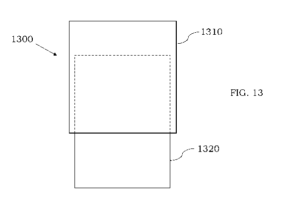
[0032] FIG. 13 is an illustration of a moveable device;
[0033] FIG. 14 is an illustration of a piston member;
[0034] FIG. 15 is an illustration of a housing;
[0035] FIG. 16 is an illustration of a piston member within a housing of a
moveable device;
[0036] FIG. 17A is an illustration showing rotational movement of a substrate;
[0037] FIG. 17B is another illustration showing rotational movement of a
substrate;
[0038] FIG. 18 is an illustration showing a cylindrical substrate;
[0039] FIG. 19A is an illustration showing a rotor;
[0040] FIG. 19B is an illustration showing a blade;
[0041] FIG. 19C is an illustration showing two work rolls;
[0042] FIG. 20 is an illustration showing a shock absorber;
[0043] FIG. 21 is an illustration showing a hydraulic or pneumatic device;
[0044] FIG. 22 is a photograph showing two coatings on different articles;
[0045] FIG. 23A and FIG. 23B are photograph showing a hard chrome coating and
an electroless
nickel coating;
[0046] FIG. 24A, FIG. 24B, FIG. 24C, FIG. 24D and FIG. 24E are photographs
showing the
results of a salt spray test on tested coatings;
[0047] FIG. 25 is a graph comparing the salt spray tests;
[0048] FIG. 26A, FIG. 26B, FIG. 26C, FIG. 26D and FIG. 26E are photographs
showing salt spray
tests and coating appearance after 5000 hours;
[0049] FIG. 27 is a photograph showing images of notched bars before and after
applying a
coating;
[0050] FIG. 28A and FIG. 28B are images of MaxShield-V1 (FIG. 28B) and
MaxShield-V2 (FIG.
28A) coatings after 6 percent elongation;
[0051] FIG. 29 is a microscopic image of MaxShield-V1 coating'
[0052] FIG. 30 is an illustration of an apparatus to measure coefficient of
friction;
[0053] FIG. 31 is an illustration showing cracks;
CA 03224559 2023-12-18
WO 2022/266532 PCT/US2022/034164
[0054] FIG. 32A and FIG. 32B are images of two carbon steel bars coated with
MaxShield-V1
after (FIG. 32B) and before (FIG. 32A) a test;
[0055] FIG. 33 is a microscope image of the steel bar of FIG. 32B;
[0056] FIG. 34 is an illustration of an apparatus used to abrade the surface
of the coating by
applying a one (1) kg load on each abrasive wheel;
[0057] FIG. 35 is a graph comparing the wear index of different coatings;
[0058] FIG. 36 is a graph showing coefficient of friction versus cycle;
[0059] FIG. 37 is a graph showing corrosion rate for different coatings;
[0060] FIG. 38A and FIG. 38B are images showing magnified as plated and heat
treated coatings;
and
[0061] FIG. 39A, FIG. 39B, FIG. 39C and FIG. 39D are images showing surface
coating.
[0062] It will be recognized by the person of ordinary skill in the art, given
the benefit of this
specification, that the layers and features shown in the figures are not
necessarily drawn to scale.
The arrangement and dimensions of the various layers and features in the
figures are not intended
to require that any one arrangement or thickness is required unless
specifically discussed in
reference to that figure.
[0063] DETAILED DESCRIPTION
[0064] There is a need for protective coating technologies for components used
in articles that
have moveable components. While various specific illustrations of devices with
a coating are
described in more detail below, the devices generally include a moveable
component that contacts
a functional fluid or other material. The term "functional fluid" refers to a
fluid that is designed
to provide a motive force or to lubricate one or more components during
movement of the piston
member, e.g., to provide a film of oil on the surface, or to otherwise be
involved during movement
of the piston member. In some cases, the functional fluid may also provide a
resistive force during
movement of the piston member. In some examples, the functional fluid can be
used to resist
movement of a piston member from a first position to a second position. One or
more surfaces of
the moveable component can include a coating, e.g., an alloy coating. The
coating can provide
wear resistance in the presence of the functional fluid during movement of the
moveable
component or may provide wear resistance to surfaces of the moveable component
external to a
housing. The moveable component typically includes an underlying substrate and
a coating on
6
CA 03224559 2023-12-18
WO 2022/266532 PCT/US2022/034164
one or more surfaces of the substrate. If desired, one or more other
components of the device can
also include a coating, e.g., a housing that works functionally with the
moveable component can
also include a coating if desired.
[0065] In certain embodiments, the materials and methods described herein can
be used to provide
a coating layer on a surface of a moveable component. The exact material or
materials in the
coating may vary and numerous different materials, coatings and layers are
described in more
detail below. Specific materials for use in specific devices are also
described in more detail below.
The exact coating thickness used may vary with different devices. For example,
coating thickness
can change depending on the application of the moveable component. Typical
coating thickness
may be less than 10 um up to 1 mm. As an example, for applications that deal
with highly corrosive
environments, the thickness can be 25-100 um, 25-200 um, 100-200 um, 50-150
um, 25-330 um,
100-300 um, 100-400 um, 100-500 um, 100-600 um, 100, 125, 150, 175, 200, 225,
250, 275, 300,
325, 350, 375, 400, 425, 450, 475, 500, 525, 550, 575, 600, 700, 725, 800,
825, 850, 875, or 900
um.
[0066] In certain embodiments, the moveable component can include one or more
layers as
described below in connection with FIGS. 1-12. Specific articles or devices
including the substrate
and/or other layers are also described. The exact material or materials in the
surface coating may
vary. In some configurations, the surface coating comprises one or more
metals. In some
embodiments, the surface coating may include a metal alloy, e.g., an alloy
comprising two or more
metals. In some embodiments, the surface coating comprises a metal alloy
including only two
metals or a metal and another material. In certain embodiments, the surface
coating comprises a
metal alloy including only three metals or a metal and two other materials. In
other embodiments,
the surface coating may contain only a single layer formed on the substrate.
For example, the
single layer can be exposed to the environment to protect the underlying
substrate from
degradation. In some instances, the surface coating may contain only a first
layer formed on the
substrate and a second layer formed on the first layer.
[0067] In some embodiments, the alloy layer may "consist essentially of' two
or more materials.
The phrase "consists essentially of' or "consisting essentially of' is
intended to refer to the
specified materials and only minor impurities and those materials that do not
materially affect the
basic characteristic(s) of the configuration. The term "consists of' refers to
only those materials
and any impurities that cannot be removed through conventional purification
techniques.
7
CA 03224559 2023-12-18
WO 2022/266532 PCT/US2022/034164
[0068] In certain embodiments, the alloy layers described herein can include
one, two or more
Group IV transition metals which include scandium, titanium, vanadium,
chromium, manganese,
iron, cobalt, nickel, copper and zinc.
[0069] In other configurations, the alloy layers described herein can include
one, two or more
Group V metals, which include yttrium, zirconium, niobium, ruthenium, rhodium,
palladium,
silver and cadmium.
[0070] In some configurations, the alloy layers described herein can include
one, two or more
Group VI metals, which include the non-radioactive lanthanides (La, Ce, Pr,
Nd, Sm, Eu, Gd, Tb,
Dy, Ho, Er, Tm, Yb and Lu), hafnium, tantalum, tungsten, rhenium, osmium,
iridium, platinum,
gold and mercury.
[0071] In other embodiments, the alloy layers described herein can include
one, two or more
Group VII metals, which include the non-radioactive actinides (Th, Pa, U).
[0072] In some instances, the alloy layers described herein can include one or
more metals from
the Group IV metals and one or more metals from the Group V metals or the
Group VI metals or
the Group VII metals.
[0073] In other instances, the alloy layers described herein can include one
or more metals from
the Group V metals and one or more metals from the Group VI metals or the
Group VII metals.
[0074] In other examples, the alloy layers described herein can include one or
more metals from
the Group VI metals and one or more metals from the Group VII metals.
[0075] In some embodiments, the alloy layers described herein includes only
two metals with one
metal from the Group IV metals and the other metal from the Group V metals,
the Group VI metals
or Group VII metals.
[0076] In some embodiments, the alloy layers described herein includes only
two metals with one
metal from the Group V metals and the other metal from the Group VI metals or
Group VII metals.
[0077] In other embodiments, the alloy layers described herein includes only
two metals with one
metal from the Group VI metals and the other metal from the Group VII metals.
[0078] In some examples, the alloy layers described herein includes only two
metals with both
metals being Group IV metals.
[0079] In some embodiments, the alloy layers described herein includes only
two metals with both
metals being Group V metals.
8
CA 03224559 2023-12-18
WO 2022/266532 PCT/US2022/034164
[0080] In some embodiments, the alloy layers described herein includes only
two metals with both
metals being Group VI metals.
[0081] In some embodiments, the alloy layers described herein includes only
two metals with both
metals being Group VII metals.
[0082] If desired, the alloy layers described herein can also include Group II
materials (Li, Be, B
and C) or Group III materials (Na, Mg, Al, Si, P, and S) in addition to, or in
place, of the other
metals. These materials may be present in combination with one, two, three or
more metals.
[0083] In some embodiments, the alloy layer described herein comprises
molybdenum and one or
more additional metals, e.g., one or more additional metals selected from the
group consisting of
Group IV metals, Group V metals, Group VI metals and Group VII metals. In
certain
embodiments, the metal alloy comprises molybdenum and only one additional
metal, e.g., only
one additional metal selected from the group consisting of Group IV metals,
Group V metals,
Group VI metals and Group VII metals. In certain embodiments, the metal alloy
comprises
molybdenum and only two additional metals or materials, e.g., only two
additional metals or
materials selected from the group consisting of Group IV metals, Group V
metals, Group VI
metals, Group VII metals, Group II materials and Group III materials. In some
embodiments, the
surface coating has a single layer formed on the substrate, where the single
layer comprises
molybdenum and one or more additional metals, e.g., one or more additional
metals selected from
the group consisting of Group IV metals, Group V metals, Group VI metals and
Group VII metals.
In certain embodiments, the surface coating has a single layer formed on the
substrate, where the
single layer comprises molybdenum and only one additional metal, e.g., only
one additional metal
selected from the group consisting of Group IV metals, Group V metals, Group
VI metals and
Group VII metals. In some examples, the surface coating has a single layer
formed on the
substrate, where the single layer comprises molybdenum and only two additional
metals or
materials, e.g., only two additional metal or material selected from the group
consisting of Group
IV metals, Group V metals, Group VI metals, Group VII metals, Group II
materials and Group III
materials.
[0084] In some embodiments, the alloy layer described herein comprises
tungsten and one or more
additional metals, e.g., one or more additional metals selected from the group
consisting of Group
IV metals, Group V metals, Group VI metals and Group VII metals. In certain
embodiments, the
metal alloy comprises tungsten and only one additional metal, e.g., only one
additional metal
9
CA 03224559 2023-12-18
WO 2022/266532 PCT/US2022/034164
selected from the group consisting of Group IV metals, Group V metals, Group
VI metals and
Group VII metals. In certain embodiments, the metal alloy comprises tungsten
and only two
additional metals or materials, e.g., only two additional metals or materials
selected from the group
consisting of Group IV metals, Group V metals, Group VI metals, Group VII
metals, Group II
materials and Group III materials. In some embodiments, the surface coating
has a single layer
formed on the substrate, where the single layer comprises tungsten and one or
more additional
metals, e.g., one or more additional metals selected from the group consisting
of Group IV metals,
Group V metals, Group VI metals and Group VII metals. In certain embodiments,
the surface
coating has a single layer formed on the substrate, where the single layer
comprises tungsten and
only one additional metal, e.g., only one additional metal selected from the
group consisting of
Group IV metals, Group V metals, Group VI metals and Group VII metals. In some
examples,
the surface coating has a single layer formed on the substrate, where the
single layer comprises
tungsten and only two additional metals or materials, e.g., only two
additional metal or material
selected from the group consisting of Group IV metals, Group V metals, Group
VI metals, Group
VII metals, Group II materials and Group III materials.
[0085] In some embodiments, the alloy layer described herein comprises nickel
and one or more
additional metals, e.g., one or more additional metals selected from the group
consisting of Group
IV metals, Group V metals, Group VI metals and Group VII metals. In certain
embodiments, the
metal alloy comprises nickel and only one additional metal, e.g., only one
additional metal selected
from the group consisting of Group IV metals, Group V metals, Group VI metals
and Group VII
metals. In certain embodiments, the metal alloy comprises nickel and only two
additional metals
or materials, e.g., only two additional metals or materials selected from the
group consisting of
Group IV metals, Group V metals, Group VI metals, Group VII metals, Group II
materials and
Group III materials. In some embodiments, the surface coating has a single
layer formed on the
substrate, where the single layer comprises nickel and one or more additional
metals, e.g., one or
more additional metals selected from the group consisting of Group IV metals,
Group V metals,
Group VI metals and Group VII metals. In certain embodiments, the surface
coating has a single
layer formed on the substrate, where the single layer comprises nickel and
only one additional
metal, e.g., only one additional metal selected from the group consisting of
Group IV metals,
Group V metals, Group VI metals and Group VII metals. In some examples, the
surface coating
has a single layer formed on the substrate, where the single layer comprises
nickel and only two
CA 03224559 2023-12-18
WO 2022/266532 PCT/US2022/034164
additional metals or materials, e.g., only two additional metal or material
selected from the group
consisting of Group IV metals, Group V metals, Group VI metals, Group VII
metals, Group II
materials and Group III materials.
[0086] In certain configurations, the alloy layer comprises (i) molybdenum and
(ii) at least one
element selected from the group consisting of nickel, tungsten, cobalt,
chromium, tin,
phosphorous, iron, magnesium and boron or at least one compound comprising one
or more of
nickel, tungsten, cobalt, chromium, tin, phosphorous, iron, magnesium or
boron. In certain
embodiments, the alloy excludes precious metals.
[0087] In certain configurations, the alloy layer described herein comprises
two or more of nickel,
molybdenum, copper, phosphorous, boron, boron nitride, silicon carbide,
aluminum oxide,
molybdenum disulfide, carbon fibers, carbon nanotubes, particles, cobalt,
tungsten, gold, platinum,
silver, or alloys or combinations thereof.
[0088] In other embodiments, the alloy layer described herein includes two or
more of nickel,
molybdenum, copper, phosphorous, boron, boron nitride, silicon carbide,
aluminum oxide,
molybdenum disulfide, carbon fibers, carbon nanotubes, particles, cobalt,
tungsten, gold, platinum,
silver, or alloys or combinations thereof.
[0089] In certain embodiments, the alloy layer described herein comprises an
alloy of (i)
molybdenum, molybdenum oxide or other compounds of molybdenum, and (ii) a
transition metal,
transition metal oxide or other compounds of a transition metal.
[0090] In certain embodiments, the alloy layer described herein includes only
two metals from (i)
molybdenum, molybdenum oxide or other compounds of molybdenum, and (ii) a
transition metal,
transition metal oxide or other compounds of a transition metal.
[0091] In certain embodiments, the metal alloy of the layers described herein
includes only two
metals from (i) tungsten, tungsten oxide or other compounds of tungsten, and
(ii) a transition metal,
transition metal oxide or other compounds of a transition metal.
[0092] In certain embodiments, the alloy layer described herein includes only
two metals from (i)
nickel, nickel oxide or other compounds of nickel, and (ii) a transition
metal, transition metal oxide
or other compounds of a transition metal. In some embodiments, the transition
metal, transition
metal oxide or other compounds of the transition metal comprises scandium,
manganese, iron,
cobalt, nickel, copper, zinc, yttrium, technetium, silver, cadmium, lanthanum,
platinum, gold,
11
CA 03224559 2023-12-18
WO 2022/266532 PCT/US2022/034164
mercury, actinium, and combinations thereof. For example, the metal alloy
coating can include a
Ni-Mo alloy, a Ni-W alloy or only have a Ni-Mo alloy or a Ni-W alloy.
[0093] In certain embodiments, the alloy layer exhibits at least two times
more corrosion
resistance compared to a chrome coating according to an ASTM B117 salt spray
corrosion test. In
some embodiments, the metal alloy layer does not exhibit hydrogen
embrittlement as tested by an
ASTM F519 standard.
[0094] In embodiments where the alloy layer includes molybdenum, molybdenum
oxide or other
compounds of molybdenum, these materials can be present in the metal alloy
coating at 35% by
weight or less (or 25% by weight or less) based on a weight of the alloy layer
or the weight of the
surface coating. In some other cases where the metal alloy layer includes
molybdenum,
molybdenum oxide or other compounds of molybdenum, these materials can be
present in the
metal alloy coating at 48% by weight or less based on a weight of the alloy
layer or the surface
coating.
[0095] In some instances, the alloy layer may consist of a single layer. In
other configurations,
two or more layers may be present in a surface coating. As noted herein, the
two layers may
comprise the same or different materials. When the materials are the same, the
materials may be
present in different amounts in the two layers or may be deposited in
different layers using different
processes.
[0096] In some embodiments, the alloy layer can include an alloy of
molybdenum, e.g.,
molybdenum in combination with one or more of nickel, chromium, carbon,
cobalt, tin, tungsten,
aluminum, vanadium, titanium, niobium, iron, boron, phosphorous, magnesium or
copper. For
example, molybdenum may be present at 35% by weight or less and the other
component can be
present at 65% by weight or more. More than two components or metals may be
present if desired.
In other embodiments, the surface coating can include an alloy of molybdenum
and one other
metal or material, e.g., molybdenum in combination with only one of nickel,
chromium, carbon,
cobalt, tin, tungsten, aluminum, vanadium, titanium, niobium, iron, boron,
phosphorous,
magnesium or copper. In some embodiments, the surface coating can include an
alloy of
molybdenum and two other metals, e.g., molybdenum in combination with only two
of nickel,
chromium, carbon, cobalt, tin, tungsten, aluminum, vanadium, titanium,
niobium, iron, boron,
phosphorous, magnesium or copper.
12
CA 03224559 2023-12-18
WO 2022/266532 PCT/US2022/034164
[0097] In some embodiments, the alloy layer can include an alloy of tungsten,
e.g., tungsten in
combination with one or more of nickel, molybdenum, chromium, carbon, cobalt,
tin, aluminum,
vanadium, titanium, niobium, iron, boron, phosphorous, magnesium or copper. In
other
embodiments, the surface coating can include an alloy of tungsten and one
other metal or material,
e.g., tungsten in combination with only one of nickel, molybdenum, chromium,
carbon, cobalt, tin,
aluminum, vanadium, titanium, niobium, iron, boron, phosphorous, magnesium or
copper. In some
embodiments, the surface coating can include an alloy of tungsten and two
other metals, e.g.,
tungsten in combination with only two of nickel, molybdenum, chromium, carbon,
cobalt, tin,
aluminum, vanadium, titanium, niobium, iron, boron, phosphorous, magnesium or
copper. In
some embodiments, the surface coating can include an alloy of tungsten, e.g.,
tungsten in
combination with one or more of chromium, molybdenum, carbon, cobalt, tin,
aluminum,
vanadium, titanium, niobium, iron, boron, phosphorous, magnesium or copper.
For example,
tungsten may be present at 35% by weight or less and the other component can
be present at 65%
by weight or more. More than two components or metals may be present if
desired. In other
embodiments, the surface coating can include an alloy of tungsten and one or
two other metals or
materials, e.g., tungsten in combination with only one of nickel, molybdenum,
chromium, carbon,
cobalt, tin, aluminum, vanadium, titanium, niobium, iron, boron, phosphorous,
magnesium or
copper. In some embodiments, the surface coating can include an alloy of
tungsten and two other
metals, e.g., tungsten in combination with only two of nickel, molybdenum,
chromium, carbon,
cobalt, tin, aluminum, vanadium, titanium, niobium, iron, boron, phosphorous,
magnesium or
copper.
[0098] In some embodiments, the surface coatings described herein may provide
desirable
performance criteria including, but not limited to, a certain surface
roughness (Ra) as described in
the ISO 4287 and ISO 4288 standards. Roughness can be measured, for example,
using a
profilometer. Coating thickness may also be measured using a non-destructive
technique such as
a magnetic measurement tool, XRF, or sampling and destructive technique such
as cross-section
analysis. The exact surface roughness (Ra) may vary, for example, and may be
equal to or less
than 1 micron or can be between 0.1 microns and 1 micron. The devices may also
have a desired
coefficient of friction (CoF). This property generally depends on both the
surfaces worn against
each other and the fluid located between them. The roughness of each surface,
the viscosity of the
fluid, and the temperature of the test can impact coefficient of friction
measurements. CoF can be
13
CA 03224559 2023-12-18
WO 2022/266532 PCT/US2022/034164
measured, for example, according to ASTM G99-17 or a block on ring test as
specified in ASTM
G77-17. The coating, or one or more layers of the coating, may provide a
specific hardness as
tested by ASTM E384-17. For example, the coating may have a hardness higher
than 600 Vickers
as measured per ASTM E384 ¨ 17. Where the coating includes more than a single
layer, any one
or more of the layers have a hardness higher than 600 Vickers as measured per
ASTM E384 ¨ 17.
In some embodiments, an outer layer of the coating may have a hardness higher
than 600 Vickers
as measured per ASTM E384 ¨ 17. In other embodiments where the coating has a
hardness of 600
Vickers or higher as measured per ASTM E384 ¨ 17, one of the layers, when
present by itself,
may have a hardness less than 600 Vickers as measured per ASTM E384 ¨ 17.
[0099] While various layers and substrates are described below in reference to
FIGS. 1-12 as
having flat surfaces, a flat surface is not required and may not be desired in
some instances. For
example, a substrate (or any of the layers or both) may have a rough surface
or be roughened
purposefully or be smoothed purposefully as desired. As an example, the
substrate may have a
textured surface including transferring texture which a partial or complete
replica of the
transferring texture shall be transferred to the other objects that come in
contact with such a surface
with transferring texture. In an embodiment, such a surface can be a part of
an article or device
that during use or movement contacts another material. For example, a steel
work roll used in cold
rolling processes where the surface of the work roll has certain transferring
texture that can be
transferred to the steel sheet during the rolling process. Another example is
the steel work roll
described in the previous embodiment where the transferring texture is made
using electrical
discharge texturing (EDT). Another embodiment is a work roll used in hot
rolling processes. In
another embodiment, a transferring texture can be a part of a mold which is
designed to transfer
the texture to another object. In an embodiment, the texture is transferred to
a metal. In an
embodiment, the texture is transferred to a polymer. In an embodiment, the
texture is transferred
to a molten metal which solidified afterward. In an embodiment, the texture is
transferred to a
liquid or fluid which solidified afterward.
[00100] In another embodiment the surface may have an adhesive roughness
designed to
increase the adhesion between such a surface and another surface or a coating
applied on top. In
an embodiment, the adhesive texture is used to increase the adhesion of the
substrate to the thermal
spray coatings. In another embodiment, the adhesive texture is used to
increase the adhesion of a
coating comprising tungsten the surface. In another embodiment, the adhesive
layer is used to
14
CA 03224559 2023-12-18
WO 2022/266532 PCT/US2022/034164
increase the adhesion of a coating comparing one or combination of nitride, a
nitride, a metal
carbide, a carbide, a boride, tungsten, tungsten carbide, a tungsten alloy, a
tungsten compound, a
stainless steel, a ceramic, chromium, chromium carbide, chromium oxide, a
chromium compound,
aluminum oxide, zirconia, titania, nickel, a nickel carbide, a nickel oxide, a
nickel alloy, a cobalt
compound, a cobalt alloy, a cobalt phosphorous alloy, molybdenum, a molybdenum
compound, a
nanocomposite, an oxide composite.
[00101] In another embodiment, the roughness is added to impact the light
reflection. In an
embodiment, the surface roughness is altered to have less roughness. In an
embodiment, the
surface roughness, Ra, may be altered to be less than 1 um. In another
embodiment, the surface
roughness is altered to be less than 0.5 um. In an embodiment, the surface
with altered roughness
is shiny. In another embodiment, the surface with altered roughness is exposed
and is required to
be touched by human. In another embodiment, the surface reflects less light
and becomes less
shiny. In an embodiment, the contact angle of water on the surface with
altered roughness is less
than the original surface.
[00102] In certain embodiments, the roughness may have irregular shapes or
respective
patterns. In certain embodiments, the roughness of the surfaces with coating,
Ra, is less than 1 um.
In another embodiment, the roughness of the surfaces with coating, Ra, is more
than 1 um and less
than 10 um. In another embodiments, the roughness of the surfaces with
coating, Ra, is more than
um and less than 100 um, in another embodiment the Ra of the surfaces is less
than 0.7. In some
embodiments, the Ra is less than 0.5 um and more than 0.05 um. In another
embodiments the Ra
is less than 0.5 um. In another embodiment, the Ra is less than 0.4 um. In
another embodiment,
the Ra is less than 0.3 um. In another embodiment, the Ra is less than 0.2 um.
In another
embodiment, the Ra is less than 0.1 um. In another embodiment, the patterns
are made using
grinding, blasting, sand blasting, abrasive blasting, sandblasting,
burnishing, grinding, honing,
mass finishing, tumble finishing, vibratory finishing, polishing, buffing,
lapping, electrochemical
etching, chemical etching, laser etching, laser patterning, or other methods.
In another method, the
surface is textured using shot blasting (SB), laser beam texturing (LBT) and
electrical discharge
texturing (EDT) or electron beam texturing (EBT) is being evaluated.
Electrical discharge
texturing (EDT) can be used on steel substrate to create textures. Textures
may be formed using
an electrodeposition techniques. Textures may be formed using thermal spray
techniques. Cross
section of the patterns may have specific geometries such as rectangles,
triangles, stars, circles or
CA 03224559 2023-12-18
WO 2022/266532 PCT/US2022/034164
a combinations of thereof. The patterns may be in the shape of ridges,
pillars, spirals, a combination
of thereof or other shapes. The Ra may be larger than 100 um. The patterns may
be created using
cutting, milling, molding and or other tools.
[00103] Certain embodiments are described in more detail below with
reference to coatings
or layers. The coatings or layers may include a single material, a combination
of materials, an
alloy, composites, or other materials and compositions as noted herein. In
embodiments where
the layer refers to a metal alloy, the metal alloy can include two or more
materials, e.g., two or
more metals. In some configurations, one metal may be present at 79% by weight
or more in the
layer and the other material may be present at 21% by weight or less in the
layer. For example,
one of the layers described herein can include a molybdenum alloy, a tungsten
alloy or a nickel
alloy. One of the materials may be present at 79% by weight or more in the
layer and the other
material(s) may be present at 21% by weight or less in the layer. Where the
metal alloy includes
molybdenum, the molybdenum can be present at 21% by weight or less or 79% by
weight or more
in the layer and the other material(s) may be present so the sum of the weight
percentages add to
100 weight percent. Alternatively, the other material(s) can be present at 79%
by weight or more
in the layer and the molybdenum may be present at 21% by weight or less in the
layer. One or
may layers can also include another metal or a metal alloy. There may also be
minor impurities
present that add negligible weight to the overall alloy layer or surface
coating.
[00104] The exact amount of each material present may be selected to
provide a layer or
article with desired performance specifications. The weight percentages can be
based on weight
of the alloy layer or the entire surface coating. In some embodiments, one
metal in a layer is
present at 35% by weight or less in the layer, e.g., is present at 34%, 33%,
32%, 31%, 30%, 29%,
28%, 27%, 26%, 25%, 24%, 23%, 22%, 21%, 20%, 19%, 18%, 17%, 16%, 15%, 14%,
13%, 12%,
10%, 9%, 8%, 7%, 6%, 5%, 4%, 3%, 2%, 1% or less by weight in the layer or in
the coating. For
example, one or more of molybdenum, tungsten or cobalt can be present in the
layer or in the
coating at 35% by weight or less, e.g., 25%, 24%, 23%, 33%, 31%, 20%, 19%,
18%, 17%, 16%,
15%, 14%, 13%, 12%, 10%, 9%, 8%, 7%, 6%, 5%, 4%, 3%, 2%, 1% or less in the
layer or the
coating. In other configurations, one or more of the layers can include a
metal in a layer that is
present at 65% by weight or more, e.g., is present at 65%, 70%, 75%, 80%, 81%,
82%, 83%, 84%,
85%, 85%, 87%, 88%, 89%, 90%, 91%, 92%, 93%, 94%, 95%, 96%, 97%, 98%, 99% or
more by
weight in the layer or in the coating. For example, nickel can be present in
the layer or in the
16
CA 03224559 2023-12-18
WO 2022/266532 PCT/US2022/034164
coating at 65%, 70%, 75%, 80%, 81%, 82%, 83%, 84%, 85%, 85%, 87%, 88%, 89%,
90%, 91%,
92%, 93%, 94%, 95%, 96%, 97%, 98%, 99% or more by weight of the alloy layer or
the surface
coating. Alternatively, molybdenum can be present in the layer or in the
coating at 65%, 70%,
75%, 80%, 81%, 82%, 83%, 84%, 85%, 85%, 87%, 88%, 89%, 90%, 91%, 92%, 93%,
94%, 95%,
96%, 97%, 98%, 99% or more by weight of the alloy layer or the surface
coating.
[00105] In some embodiments, the alloy layers described herein may be
present without any
precious metals. The term "precious metals" refers to gold, silver, ruthenium,
rhodium, palladium,
osmium, iridium, and platinum. For example, the alloy layer (and/or the entire
surface coating)
can be free of (has none of) each of gold, silver, ruthenium, rhodium,
palladium, osmium, iridium,
and platinum. Omission of the precious metals can reduce overall cost.
[00106] In certain embodiments, where nickel is present in a metal alloy
layer, the nickel
can be present without any tungsten or cobalt in that same layer. For example,
where a layer
comprises a nickel alloy, the layer has neither of tungsten or cobalt, e.g.,
0% by weight of the
cobalt or tungsten is present. That layer may also have 0% by weight precious
metals.
[00107] In certain examples, the alloy layers can include non-metal
materials and additives
as desired. For example, particles, nanoparticles, nanomaterials or other
materials that include one
or more of polytetrafluoroethylene (PTFE), SiC, SiO2, diamond, graphite,
graphene, boron, boride,
functionalized silicon particles, fluorosilicone, siloxanes, TiO2, nanotubes
and nanostructures may
be present in the metal alloy layer. Additional materials are described in
more detail below.
[00108] In some examples, one of the metals of the layers described herein
is nickel. For
example, nickel, nickel alloys, nickel compounds, nickel composites, a nickel-
phosphorous alloy,
a nickel-molybdenum alloy, a nickel-molybdenum-phosphorous alloy, a nickel-
cobalt alloy, a
nickel-tungsten alloy, a nickel-cobalt-phosphorus alloy, a nickel-tungsten-
phosphorous alloy, a
nickel alloy containing only nickel and molybdenum, nickel alloys including at
least nickel and a
transition metal, nickel alloys including at least two metals other than any
precious metals, a nickel
alloy including at least nickel and a refractory metal other than any precious
metals, a nickel alloy
including at least nickel and a refractory metal excluding tungsten, a nickel
alloy including at least
nickel and a refractory metal excluding tungsten and any precious metals, a
nickel alloy including
at least nickel and a excluding cobalt and any precious metals, a composite
alloy containing nickel
and particles, a composite alloy containing nickel and nanoparticles, a
composite alloy containing
nickel and SiO2, SiC or other silicon compounds, a composite alloy containing
nickel and boride,
17
CA 03224559 2023-12-18
WO 2022/266532 PCT/US2022/034164
brome nitride or other boron compounds, a composite alloy containing nickel
and PTFE or other
fluorine compounds, a composite alloy containing nickel, molybdenum and
chrome, chromium
carbide, chromium oxide or other chrome compounds may be present in one or
more of the layers
described herein.
[00109] In certain embodiments, one of the metals of the alloy layers
described herein is
molybdenum. For example, molybdenum, a molybdenum alloy, molybdenum composite,
a
molybdenum-tin alloy, an alloy containing at least molybdenum and nickel, an
alloy containing at
least molybdenum and tin, an alloy containing at least molybdenum and cobalt,
an alloy containing
at least molybdenum and phosphorous, an alloy containing only nickel and
molybdenum, an alloy
containing only tin and molybdenum, an alloy containing only cobalt and
molybdenum, an alloy
containing only nickel, molybdenum and phosphorous, a molybdenum alloy
including at least two
metals other than precious metals, a molybdenum alloy including at least
molybdenum and a
transition metal, a molybdenum alloy including at least molybdenum and a
transition metal other
than precious metals, a molybdenum alloy including at least two metals
excluding substances of
very high concern under European law, a composite alloy including molybdenum
and particles, a
composite alloy including molybdenum and soft particles, a composite alloy
including
molybdenum and nanoparticles, a composite alloy containing molybdenum and
SiO2, SiC or other
silicon compounds, a composite alloy containing molybdenum and boride, brome
nitride or other
boron compounds, a composite alloy containing molybdenum and PTFE or other
fluorine
compounds, a composite alloy containing molybdenum and chrome, chromium
carbide, chromium
oxide or other chrome compounds may be present in one or more of the layers
described herein.
[00110] In another embodiment, one of the metals of the alloy layers
described herein is
cobalt. For example, cobalt, cobalt alloys, cobalt compounds, cobalt
composites, a cobalt-
phosphorous alloy, a cobalt-molybdenum alloy, a cobalt-molybdenum-phosphorous
alloy, a
cobalt-tungsten alloy, a cobalt-tungsten-phosphorous alloy, cobalt alloy
containing only cobalt and
molybdenum, cobalt alloys including at least cobalt and a transition metal,
cobalt alloys including
at least two metals excluding precious metals, a cobalt alloy including at
least cobalt and a
refractory metal excluding precious metals, a cobalt alloy including at least
cobalt and a refractory
metal excluding tungsten, a cobalt alloy including at least cobalt and a
refractory metal excluding
tungsten and precious metals, a cobalt alloy including at least cobalt and
excluding nickel and
precious metals, a composite alloy containing cobalt and particles, a
composite alloy containing
18
CA 03224559 2023-12-18
WO 2022/266532 PCT/US2022/034164
cobalt and nanoparticles, a composite alloy containing cobalt and SiO2, SiC or
other silicon
compounds, a composite alloy containing cobalt and boride, brome nitride or
other boron
compounds, a composite alloy containing cobalt and PTFE or other fluorine
compounds, a
composite alloy containing cobalt, molybdenum and chrome, chromium carbide,
chromium oxide
or other chrome compounds.
[00111] In some embodiments, one of the metals of the alloy layers
described herein is tin.
For example, tin, tin alloys, tin compounds, tin composites, a tin-phosphorous
alloy, a tin-
molybdenum alloy, a tin-molybdenum-phosphorous alloy, a tin-tungsten alloy, a
tin-tungsten-
phosphorous alloy, a tin alloy containing only tin and molybdenum, tin alloys
including at least
tin and a transition metal, tin alloys including at least two metals excluding
precious metals, a tin
alloy including at least tin and a refractory metal excluding precious metals,
a tin alloy including
at least tin and a refractory metal excluding tungsten, a tin alloy including
at least tin and a
refractory metal excluding tungsten and precious metals, a tin alloy including
at least tin and
excluding nickel and precious metals, a composite alloy containing tin and
particles, a composite
alloy containing tin and nanoparticles, a composite alloy containing tin and
SiO2, SiC or other
silicon compounds, a composite alloy containing tin and boride, brome nitride
or other boron
compounds, a composite alloy containing tin and PTFE or other fluorine
compounds, a composite
alloy containing tin, molybdenum and chrome, chromium carbide, chromium oxide
or other
chrome compounds.
[00112] In another embodiment, one of the metals of the alloy layers
described herein is
tungsten. For example, tungsten, tungsten alloys, tungsten compounds, tungsten
composites, a
tungsten-phosphorous alloy, a tungsten-molybdenum alloy, a tungsten-molybdenum-
phosphorous
alloy, a tungsten alloy containing only tungsten and molybdenum, a tungsten
alloy including at
least tungsten and a transition metal, a tungsten alloy including at least two
metals excluding
precious metals, a tungsten alloy including at least tungsten and a refractory
metal excluding
precious metals, a tungsten alloy including at least tungsten and excluding
nickel and precious
metals, a composite alloy containing tungsten and particles, a composite alloy
containing tungsten
and nanoparticles, a composite alloy containing tungsten and SiO2, SiC or
other silicon
compounds, a composite alloys containing tungsten and boride, brome nitride or
other boron
compounds, a composite alloy containing tungsten and PTFE or other fluorine
compounds, a
19
CA 03224559 2023-12-18
WO 2022/266532 PCT/US2022/034164
composite alloy containing tungsten, molybdenum and chrome, chromium carbide,
chromium
oxide or other chrome compounds.
[00113] In certain embodiments, one or more of the alloy layers described
herein may be
considered a "hard" layer. The hard layer typically has a Vickers hardness
higher than the substrate
and/or any underlying layers. While not required, the hard layer is typically
present as an outer
layer. In some embodiments, the hard layer may comprise one or more of a
nitride, a metal nitride,
a carbide, a metal carbide, a boride, a metal boride, tungsten, tungsten
carbide, a tungsten alloy, a
tungsten compound, a stainless steel, a ceramic, chromium, chromium carbide,
chromium oxide,
a chromium compound, aluminum oxide, zirconia, titania, nickel, a nickel
carbide, a nickel oxide,
a nickel alloy, a cobalt compound, a cobalt alloy, a cobalt phosphorous alloy,
molybdenum, a
molybdenum compound, a nanocomposite, an oxide composite, or combinations
thereof.
[00114] In certain embodiments, a simplified illustration of a substrate
and an alloy layer of
a surface coating is shown in FIG. 1. An article or device 100 includes a
substrate 105 (which is
shown as a section in FIG. 1) and a first layer 110 on a first surface 106 of
the substrate 105. While
not shown, a layer or coating may also be present on surfaces 107, 108 and 109
of the substrate
105. The layer 110 is shown in FIG. 1 as a solid layer with uniform thickness
present across the
surface 106 of the substrate 105. This configuration is not required, and
different areas of the layer
110 may include different thicknesses or even different materials. Further,
certain areas of the
surface 106 may not include any surface coating at all. In some embodiments,
the substrate 105
may be, or may include, a metal material including, but not limited to, steel
(carbon steel, tool
steel, stainless steel, etc.), copper, copper alloys, aluminum, aluminum
alloys, chromium,
chromium alloys, nickel, nickel alloys, titanium, titanium alloys, nickel-
chromium superalloys,
nickel-molybdenum alloys, brass, Hastelloy, Inconel, Nichrome, Monel, other
substrates that
include at least one metal or substrates that are nitrided or carburized. In
some embodiments, the
substrate may be porous or may be non-porous. The layer 110 typically includes
one or more
metals or two or more metals or three or more metals or materials. For
example, the layer 110 can
be a metal alloy formed from two or more metals. In some embodiments, the
layer 110 is an alloy
layer formed from only two metals or two materials. In some examples, the
layer 110 is the only
layer present in the surface coating. In certain examples, the layer 110 is an
outer or exposed
layer such that the layer can contact surrounding fluid or other materials and
protect the underlying
substrate 105 and any layers between the layer 110 and the substrate 105.
CA 03224559 2023-12-18
WO 2022/266532 PCT/US2022/034164
[00115] In some embodiments, one of the metals in the layer 110 is nickel.
In other
embodiments, one of the metals in the layer 110 is molybdenum. In other
embodiments, one of the
metals in the layer 110 is tungsten. In other embodiments, one of the metals
in the layer 110 is
cobalt. In an additional embodiment, one of the metals in the layer 110 is
molybdenum in the form
of a molybdenum alloy. In other embodiments, the layer 110 can include a
nickel alloy, a
molybdenum alloy, a cobalt alloy, a tungsten alloy, or combinations thereof.
In other examples,
the layer 110 may be a nickel molybdenum alloy. In certain configurations, the
layer 110 may
consist of a nickel molybdenum alloy with no other materials being present in
the layer 110. In
some configurations, the layer 110 may comprise a nickel molybdenum
phosphorous alloy. In
some configurations, the layer 110 may consist of a nickel molybdenum
phosphorous alloy with
no other materials being present in the layer 110.
[00116] In some configurations, the exact thickness of the layer 110 may
vary 1 micron to
about 2 mm depending on the device where the layer 110 is present. For
example, the layer 110
may have a thickness from about 5 microns to about 1 mm or about 7 microns to
about 900
microns. Where multiple layers are present in a surface coating each layer may
have a thickness
from 1 micron to about 2 mm or the total thickness of all layers may be about
1 micron to about 2
mm.
[00117] In certain embodiments, the layer 110 can also include other
materials, e.g.,
particles, fibers, non-metals (for example, phosphorous, boron, boron nitride,
silicon compounds
such as silicon dioxide, silicon carbide, etc.), aluminum oxide, molybdenum
disulfide, carbon
fibers, carbon nanotubes, cobalt, tungsten, tin, gold, platinum, silver and
combinations thereof.
The particles can be soft particles such as polymer particles, PTFE particles,
fluoropolymers, and
other soft particles. The particles can be hard particles such as diamond,
boron, boron nitride,
silicon compounds such as silicon dioxide, silicon carbide, etc. The particles
can be hydrophobic
or hydrophilic. Hydrophobic particles such PTFE particles, Teflon particles,
Fluoropolymers,
silicon base particles, hard particles functionalized in hydrophobic,
hydrophilic or both groups.
Such as silicon dioxide or silicon carbide functionalized in fluoro-
compounds, molecules
containing florin, silicon compounds, molecules containing silicon, and other
polymers. Other
particles such as titanium dioxide, and other catalyst may be used as well
either functionalized or
as is.
21
CA 03224559 2023-12-18
WO 2022/266532 PCT/US2022/034164
[00118] In other configurations, the layer 110 can include a nickel
molybdenum alloy, a
nickel molybdenum alloy where a weight percentage of the molybdenum is less
than 35% by
weight, a nickel molybdenum phosphorous alloy where a weight percentage of the
molybdenum
is less than 35% by weight, a ductile alloy of a refractory metal with nickel,
a ductile alloy of
nickel and molybdenum, a brittle alloy of a refractory metal with nickel, a
ductile alloy of nickel
and molybdenum, a brittle alloy of a transition metal with molybdenum, a
ductile alloy of a
transition metal with molybdenum, an alloy of nickel and molybdenum with a
hardness less than
1100 and higher than 500 Vickers, a nickel molybdenum alloy that provides a
surface roughness
Ra less than 1 micrometer, a nickel molybdenum alloy with uniform and non-
uniform grain sizes,
a nickel molybdenum alloy with an average grain size less than 2 microns, a
conformal nickel
molybdenum alloy, an alloy of nickel, molybdenum and phosphorous, an alloy of
cobalt and
molybdenum, an alloy of cobalt and molybdenum and phosphorous, an alloy of
nickel,
molybdenum and tungsten, an alloy of nickel with a material having a less
magnetic property than
nickel, an alloy of molybdenum with a material having a less hardness than
molybdenum, a
conformal alloy of a refractory metal and nickel, a ductile alloy of nickel
molybdenum, a ductile
alloy of nickel tungsten, a brittle alloy of nickel tungsten, a ductile alloy
of nickel cobalt, a brittle
alloy of nickel cobalt, an alloy of nickel and a material with a higher
temperature resistance than
nickel, a nickel molybdenum alloy where it contains a third element including
but not limited to a
refractory metal, a precious metal, hard particles, soft particles,
hydrophobic particles, hydrophilic
particles, catalysis, a material more conductive than nickel, a material more
conductive than
molybdenum, a material softer than nickel, a material harder than nickel and
less hard than
molybdenum, or other compounds such as phosphorous, boron, boron nitride,
silicon carbide,
silicone oxide, aluminum oxide, molybdenum disulfide, hard particles with a
hardness of HV
greater than 750 Vickers, and/or hard particles with size less 1 micron, a
nickel molybdenum alloy
where it contains a third element including but not limited to a refractory
metal, a precious metal,
hard particles, a material more conductive than nickel, a material more
conductive than
molybdenum, a material softer than nickel, or other compounds such as
phosphorous, boron, boron
nitride, silicon carbide, silicone oxide, aluminum oxide, molybdenum
disulfide, hard particles with
a hardness of HV greater than 750 Vickers, and/or hard particles with size
less 1 micron.
[00119] In some instances, the layer 110 on the substrate 105 can include
a nickel tungsten
alloy or a nickel tungsten alloy where it contains a third element including,
but not limited to, an
22
CA 03224559 2023-12-18
WO 2022/266532 PCT/US2022/034164
element that is a refractory metal, a precious metal, hard particles or other
compounds such as
phosphorous, boron, boron nitride, silicon carbide, aluminum oxide, molybdenum
disulfide, hard
particles with hardness of HV>750, hard particles with size less 500 nm,
highly conductive
particles, carbon nanotubes and/or carbon nano-particles. Combinations of
these materials may
also be present in the layer 110 on the substrate 105.
[00120] In some embodiments, a simplified illustration of another device
is shown in FIG.
2. In this illustration, the article or the device 200 includes an
intermediate layer 210 between the
layer 110 and the underlying substrate 105. In some examples, the intermediate
layer 210 can
improve adhesion, can improve corrosion, can brighten the coating or any
combination thereof.
For example, nickel, nickel alloys, copper alloys, nickel compounds, nickel
composites, nickel-
phosphorous alloy, nickel-molybdenum alloy, nickel-molybdenum-phosphorous
alloy, nickel-
cobalt alloy, nickel-tungsten alloy, nickel-cobalt-phosphorus alloy, copper,
nickel-tungsten-
phosphorous alloy copper alloys, copper composites, tin, tin alloy, tin
composite, cobalt, cobalt
alloy, cobalt composite, cobalt-molybdenum alloy, cobalt-tungsten alloy,
cobalt-molybdenum-
phosphorous alloy, cobalt-tungsten-phosphorous alloy, molybdenum, molybdenum
alloy,
molybdenum composite, nickel alloys including at least two metals excluding
precious metals,
molybdenum alloy including at least two metals excluding precious metals,
molybdenum alloy
including at least molybdenum and a transition metal, molybdenum alloy
including at least
molybdenum and a transition metal excluding precious metals, metals tungsten
alloys, nickel
alloys including at least nickel and a refractory metal, nickel alloy
including at least nickel and a
refractory metal (excluding precious metals), molybdenum-tin alloy, tungsten
alloys, tungsten
composite, or other materials may be present as a layer 210, between the layer
110 and the substrate
105 to improve adhesion between the layer 110 and the layer 210. Such a layer
can be less than 10
um, 9 um, 8 um, 7 um, 2 um, 1 um, 0.75 um, 0.5 um, or 0.25 um thick. As noted
herein, in some
instances, the layer 210 may be a strike layer, e.g., a nickel layer, added to
the substrate 105 to
improve adhesion between the substrate 105 and the layer 110.
[00121] In certain configurations, the layer 210 can function as a
brightener to increase the
overall shiny appearance of the article or device 200. A bright or semi-bright
layer generally
reflects a higher percentage of light than the layer 110. For example, nickel,
nickel alloys, copper
alloys, nickel compounds, nickel composites, nickel-phosphorous alloy, nickel-
molybdenum
alloy, nickel-molybdenum-phosphorous alloy, nickel-cobalt alloy, nickel-
tungsten alloy, nickel-
23
CA 03224559 2023-12-18
WO 2022/266532 PCT/US2022/034164
cobalt-phosphorus alloy, copper, nickel-tungsten- phosphorous alloy copper
alloys, copper
composites, tin, tin alloy, tin composite, cobalt, cobalt alloy, cobalt
composite, cobalt-
molybdenum alloy, cobalt-tungsten alloy, cobalt-molybdenum-phosphorous alloy,
cobalt-
tungsten-phosphorous alloy, molybdenum, molybdenum alloy, molybdenum
composite, nickel
alloys including at least two metals excluding precious metals, molybdenum
alloy including at
least two metals excluding precious metals, molybdenum alloy including at
least molybdenum and
a transition metal, molybdenum alloy including at least molybdenum and a
transition metal
excluding precious metals, metals tungsten alloys, nickel alloys including at
least nickel and a
transition metal, nickel alloy including at least nickel and a refractory
metal excluding precious
metals, tungsten alloys, tungsten composite, or other materials may be present
as a layer 210,
between the layer 110 and the substrate 105 to brighten the overall coating
appearance.
[00122] In other configurations, the layer 210 can act to increase
corrosion resistance of the
article or device 200. For example, nickel, nickel alloys, copper alloys,
nickel compounds, nickel
composites, nickel-phosphorous alloy, nickel-molybdenum alloy, nickel-
molybdenum-
phosphorous alloy, nickel-cobalt alloy, nickel-tungsten alloy, nickel-cobalt-
phosphorus alloy,
copper, nickel-tungsten- phosphorous alloy copper alloys, copper composites,
tin, tin alloy, tin
composite, cobalt, cobalt alloy, cobalt composite, cobalt-molybdenum alloy,
cobalt-tungsten alloy,
cobalt-molybdenum-phosphorous alloy, cobalt-tungsten-phosphorous alloy,
molybdenum,
molybdenum alloy, molybdenum composite, molybdenum-tin alloys, alloy
containing at least
molybdenum and nickel, alloy containing at least molybdenum and tin, alloy
containing at least
molybdenum and cobalt, composites including molybdenum and particles,
composites including
molybdenum and soft particles, composites including molybdenum and
nanoparticles, composites
including molybdenum and hard particles, nickel alloys including at least two
metals excluding
precious metals, molybdenum alloy including at least two metals excluding
precious metals,
molybdenum alloy including at least molybdenum and a transition metal,
molybdenum alloy
including at least molybdenum and a transition metal excluding precious
metals, tungsten alloys,
nickel alloys including at least nickel and a transition metal, nickel alloy
including at least nickel
and a refractory metal excluding precious metals, nickel alloy including at
least nickel and a
refractory metal excluding tungsten, nickel alloy including at least nickel
and a refractory metal
excluding tungsten and precious metals, tungsten alloys, a tungsten composite,
tungsten alloys
excluding alloys containing both nickel and tungsten, chrome, chrome
compounds, or other
24
CA 03224559 2023-12-18
WO 2022/266532 PCT/US2022/034164
materials may be present as a layer 210, between the layer 110 and the
substrate 105 to increase
corrosion resistance.
[00123] In some embodiments, the substrate 105 used with the intermediate
layer 210 may
be, or may include, a metal material including, but not limited to, steel
(carbon steel, tool steel,
stainless steel, alloy steel, low alloy steel, etc.), copper, copper alloys,
aluminum, aluminum alloys,
chromium, chromium alloys, nickel, nickel alloys, molybdenum, molybdenum
alloys, titanium,
titanium alloys, nickel-chromium superalloys, nickel-molybdenum alloys, brass,
bronze, a
superalloy, Hastelloy, Inconel, Nichrome, Monel, or combinations thereof. In
some embodiments,
the substrate may be porous or may be non-porous. In certain embodiments, the
layer 210 can
include one or more materials selected from the group consisting of Group II
materials, Group III
materials, a Group IV metal, a Group V metal, a Group VI metal and a Group VII
metal. In some
examples, the layer 210 is free of any precious metals. In other instances,
the layer 210 only
includes a single metal but may include other non-metal materials.
[00124] In certain embodiments, the layer 110 used with the intermediate
layer 210 typically
includes one or more metals or two or more metals. For example, the layer 110
used with the
intermediate layer 210 can include any of those materials and configurations
described in reference
to FIG. 1. For example, the layer 110 used with the layer 210 be a metal alloy
formed from two
or more metals. In some embodiments, one of the metals in the layer 110 used
with the
intermediate layer 210 is nickel. In other embodiments, one of the metals in
the layer 110 used
with the intermediate layer 210 is molybdenum. In an additional embodiment,
one of the metals in
the layer 110 used with the intermediate layer 210 is tungsten. In an
additional embodiment, one
of the metals in the layer 110 used with the intermediate layer 210 is cobalt.
In an additional
embodiment, one of the metals in the layer 110 used with the intermediate
layer 210 is chrome. In
some embodiments, the layer 110 used with the layer 210 can include only two
metals or two
materials or three metals or three materials. For example, the layer 110 used
with the layer 210
can include only nickel and molybdenum or only nickel, molybdenum and
phosphorous or only
nickel and tungsten or only nickel and cobalt or only nickel, phosphorous and
iron or only nickel
and phosphorous.
[00125] In other embodiments, the layer 110 used with the intermediate
layer 210 can
include a nickel alloy, a molybdenum alloy, a tungsten alloy, a cobalt alloy,
a chrome alloy, or
combinations thereof. In other examples, the layer 110 used with the
intermediate layer 210 may
CA 03224559 2023-12-18
WO 2022/266532 PCT/US2022/034164
be a nickel, nickel-molybdenum alloy, nickel-cobalt alloy, nickel-tungsten
alloy, nickel-
phosphorous ally, cobalt, cobalt-molybdenum alloy, cobalt-tungsten alloy,
cobalt-phosphorous
alloy, nickel-molybdenum-phosphorous alloy, cobalt-molybdenum-phosphorous
alloy, cobalt-
tungsten-phosphorous alloy, chrome, chrome alloy, molybdenum-tin alloy, chrome
compounds.
In certain configurations, the layer 110 used with the intermediate layer 210
may consist of a
nickel-molybdenum alloy with no other materials being present in the layer
110. In other
configurations, the layer 110 used with the intermediate layer 210 may consist
of a nickel-
molybdenum-phosphorous alloy with no other materials being present in the
layer 110. In other
configurations, the layer 110 used with the intermediate layer 210 may consist
of a cobalt-
molybdenum alloy with no other materials being present in the layer 110. In
other configurations,
the layer 110 used with the intermediate layer 210 may consist of a cobalt-
molybdenum-
phosphorous alloy with no other materials being present in the layer 110. In
other configurations,
the layer 110 used with the intermediate layer 210 may consist of a nickel
alloy including at least
two metals excluding precious metals. In other configurations, the layer 110
used with the
intermediate layer 210 may consist of a molybdenum alloy including at least
two metals excluding
precious metals. In other configurations, the layer 110 used with the
intermediate layer 210 may
consist of a molybdenum alloy including at least molybdenum and a transition
metal. In other
configurations, the layer 110 used with the intermediate layer 210 may consist
of a molybdenum
alloy including at least molybdenum and a transition metal excluding precious
metals. The exact
thickness of the layer 110 used with the intermediate layer 210 may vary from
1 micron to about
2 mm depending on the article where the layer 110 is present. For example, the
layer 110 may be
about 10 microns to about 200 microns thick. Similarly, a thickness of the
intermediate layer 210
may vary from 0.1 micron to about 2 mm, e.g., about 1 micron to about 20
microns. The thickness
of the layer 210 can be less than a thickness of the layer 110 or more than a
thickness of the layer
110.
[00126] In another configuration, two or more layers may be present on an
underlying substrate.
Referring to FIG. 3, an article or device 300 is shown that includes a first
layer 110 and a second
layer 320 on a substrate 105. The ordering of the layers 110, 320 could be
reversed, so the layer
320 is closer to the substrate 105 if desired. The layers 110, 320 can include
the same or different
materials or may include similar materials that have been deposited in a
different manner or under
different conditions. For example, the layers 110, 320 in FIG. 3 can
independently be any of those
26
CA 03224559 2023-12-18
WO 2022/266532 PCT/US2022/034164
materials described herein, e.g., any of those materials described in
reference to the layers of FIG.
1 or FIG. 2. In some configurations, the layers 110, 320 can each be an alloy
layer. For example,
each of the layers 110, 320 can include one or more of nickel, copper,
molybdenum, cobalt or
tungsten. The layers may be formed in similar or different manners. For
example, the layer 110
may be electrodeposited under basic conditions, and the layer 220 may be
electrodeposited under
acidic conditions. As another example, the layers 110, 320 can each
independently include nickel,
copper, molybdenum, cobalt or tungsten, but the layer 110 may be
electrodeposited under basic
conditions and the layer 220 may be deposited using a physical vapor
deposition technique, a
chemical vapor deposition, an atomic layer deposition, thermal spray technique
or other methods.
The layers 110, 320 can include metals other than copper, e.g., nickel,
molybdenum, cobalt,
tungsten, tin etc. or non-metals or both. The different conditions can provide
a different overall
structure in the layers 110, 320 even though similar materials may be present.
In certain
configurations, the layer 110 can improve adhesion of the layer 320. In other
configurations, the
layer 110 can "brighten" the surface of the device 300 so the device 300 has a
shinier overall
appearance.
[00127] In some embodiments, the substrate 105 used with the layers 110, 320
may be, or may
include, a metal material including, but not limited to, steel (carbon steel,
tool steel, stainless steel,
alloy steel, low alloy steel, etc.), copper, copper alloys, aluminum, aluminum
alloys, chromium,
chromium alloys, nickel, nickel alloys, molybdenum, molybdenum alloys,
titanium, titanium
alloys, nickel-chromium superalloys, nickel-molybdenum alloys, brass, bronze,
a superalloy,
Hastelloy, Inconel, Nichrome, Monel, or combinations thereof. In some
embodiments, the
substrate 105 may be porous or may be non-porous. The layers 110, 320
typically each includes
one or more metals or two or more metals. For example, the layers 110, 320 can
be a metal alloy
formed from two or more metals. In some embodiments, one of the metals in the
layers 110, 320
is nickel. In other embodiments, one of the metals in the layers 110, 320 is
molybdenum. In an
additional embodiment, one of the metals in the layers 110, 320 is cobalt. In
an additional
embodiment, one of the metals in the layers 110, 320 is tungsten. The layers
110, 320 need not
have the same metal and desirably the metal in the layers 110, 320 is
different. In other
embodiments, the layers 110, 320 independently can include a nickel alloy, a
molybdenum alloy,
or combinations thereof. In other examples, the layers 110, 320 independently
may be a nickel-
molybdenum alloy, a nickel-molybdenum-phosphorous alloy, a tungsten alloy, a
nickel-tungsten
27
CA 03224559 2023-12-18
WO 2022/266532 PCT/US2022/034164
alloy, etc. In certain configurations, one or both of the layers 110, 320 may
consist of a nickel
molybdenum alloy with no other materials being present in each layer. In other
configurations,
one of the layers 110, 320 may consist of a nickel-molybdenum-phosphorous
alloy with no other
materials being present in each layer. In some configurations, both of the
layers 110, 320 may
consist of a nickel-molybdenum-phosphorous alloy with no other materials being
present in each
layer. In other configurations, one or both of the layers 110, 320 may consist
of a nickel alloy
including at least nickel and a transition metal. In other configurations, one
or both of the layers
110, 320 may consist of a nickel alloy including at least nickel and a
transition metal excluding
precious metals. In other configurations, one or both of the layers 110, 320
may consist of a
molybdenum alloy including at least molybdenum and a transition metal. In
other configurations,
one or both of the layers 110, 320 may consist of a molybdenum alloy including
at least
molybdenum and a transition metal excluding precious metals. The exact
thickness of the layers
110, 320 may vary from 0.1 micron to about 2 mm depending on the device where
the coating is
present, and the thickness of the layers 110, 320 need not be the same. The
layer 110 may be
thicker than the layer 320 or may be less thick than the layer 320.
[00128] In certain configurations, an intermediate layer may be present
between the first layer
110 and the second layer 320. The intermediate layer can include, for example,
any of those
materials described in reference to layer 210 herein. Alternatively, an
intermediate layer may be
present between the substrate 105 and the layer 110 when the coating includes
the first layer 110
and the second layer 120. In some embodiments, the layer 320 may have a higher
hardness than
the layer 110. For example, a hardness of the layer 320 may be greater than
750 Vickers. In certain
embodiments, the layer 320 may comprise one or more of a nitride, a metal
nitride, a carbide, a
metal carbide, a boride, a metal boride, tungsten, tungsten carbide, a
tungsten alloy, a tungsten
compound, a stainless steel, a ceramic, chromium, chromium carbide, chromium
oxide, a
chromium compound, aluminum oxide, zirconia, titania, nickel, a nickel
carbide, a nickel oxide, a
nickel alloy, a cobalt compound, a cobalt alloy, a cobalt phosphorous alloy,
molybdenum, a
molybdenum compound, a nanocomposite, an oxide composite, or combinations
thereof.
[00129] In other embodiments, a surface of the substrate may be treated or
include a transferred
surface, e.g., a carburized, nitrated, carbonitride, induction hardening, age
hardening, precipitation
hardening, gas nitriding, normalizing, subzero treatment, annealing, shot
pinning, or chemically,
thermally, or physically or a combination of thereof, modified surface, that
is coated or treated
28
CA 03224559 2023-12-18
WO 2022/266532 PCT/US2022/034164
with one or more other layers. Referring to FIG. 4A, an article or device 400
is shown that includes
a transferred surface or a treated surface 410 on a substrate 105. The article
or device 400 also
includes a layer 110 on the treated surface 410. The layer 110 can be any of
those materials
described herein in reference to the layer 110 in FIGS. 1-3, 5A, 5B and 12. If
desired and as shown
in FIG. 4B, a layer 420 can be present between the treated surface 410 and the
layer 110 of a device
450. The thickness of the layer/treated surface 410 may vary, for example,
from about 0.1 microns
to about 50 millimeters. The treated surface 410 can be harder than the
underlying substrate 105
if desired. For example, the treated surface 410 may have a case hardness of
50-70 HRC. Where
the treated surface/layer 410 is a transferred surface, the base material can
be, but is not limited to,
a steel (low carbon steel, stainless steel, nitride steel, a steel alloy, low
alloy steel, etc.) or other
metal based materials. The exact result of treatment may vary and typically
treatment may be
performed to enhance adhesion, alter surface roughness, improve wear
resistance, improve the
internal stress, reduce the internal stress, alter the hardness, alter
lubricity, or for other reasons.
The layer 110 may be used to protect device 450 against corrosion, wear, heat
and other impacts.
In some cases, the treated surface 410 can negatively reduce the resistance of
device 450 against
corrosion, wear, corrosion and wear combined, heat, heat and wear combined,
corrosion and heat
combined or other scenario and the layer 110 may be used to improve the
performance as needed.
[00130] In some embodiments, the substrate 105 in FIGS. 4A and 4B may be, or
may include, a
metal material including, but not limited to, steel (carbon steel, tool steel,
stainless steel, alloy
steel, low alloy steel, etc.), copper, copper alloys, aluminum, aluminum
alloys, chromium,
chromium alloys, nickel, nickel alloys, molybdenum, molybdenum alloys,
titanium, titanium
alloys, nickel-chromium superalloys, nickel-molybdenum alloys, brass, bronze,
a superalloy,
Hastelloy, Inconel, Nichrome, Monel, or combinations thereof. In some
embodiments, the
substrate 105 may be porous or may be non-porous. The layer 110 in FIGS. 4A
and 4B typically
includes one or more metals or two or more metals as noted in connection with
FIGS. 1-3, 5A, 5B
and 12 herein. For example, the layer 110 in FIGS. 4A and 4B can be a metal
alloy formed from
two or more metals. In some embodiments, one of the metals in the layer 110 in
FIGS. 4A and 4B
is nickel. In other embodiments, one of the metals in the layer 110 in FIGS.
4A and 4B is
molybdenum. In an additional embodiment, one of the metals in the layer 110 in
FIGS. 4A and
4B is cobalt. In an additional embodiment, one of the metals in the layer 110
in FIGS. 4A and 4B
is tungsten. In an additional embodiment, one of the metals in the layer 110
in FIGS. 4A and 4B
29
CA 03224559 2023-12-18
WO 2022/266532 PCT/US2022/034164
is tin. In an additional embodiment, one of the metals in the layer 110 in
FIGS. 4A and 4B is
chromium. In other embodiments, the layer 110 in FIGS. 4A and 4B can include a
nickel alloy, a
molybdenum alloy, or combinations thereof. In other embodiments, the layer 110
in FIGS. 4A and
4B can include a molybdenum alloy including at least two metals (optionally
excluding precious
metals), a molybdenum alloy including at least molybdenum and a transition
metal, a molybdenum
alloy including at least molybdenum and a transition metal excluding precious
metals. In other
embodiments, the layer 110 in FIGS. 4A and 4B can include a nickel alloy
including at least two
metals excluding precious metals, nickel alloy including at least nickel and a
refractory metal,
nickel alloy including at least nickel and a refractory metal excluding
precious metals. In other
examples, the layer 110 in FIGS. 4A and 4B may be a nickel-molybdenum alloy or
a nickel-
molybdenum-phosphorous alloy. In certain configurations, the layer 110 in
FIGS. 4A and 4B may
consist of a nickel molybdenum alloy or a nickel molybdenum phosphorous alloy
with no other
materials being present in the layer 110. In other configurations, the layer
110 can include any of
those materials, and material combinations, described in reference to FIG. 1,
FIG. 2, or FIG. 3.
[00131] In certain embodiments, the exact thickness of the layer 110 in FIGS.
4A and 4B may
vary from 1 micron to about 2 mm depending on the article or device where the
layer 110 is present,
e.g., the thickness may vary from about 5 microns to about 200 microns.
[00132] In certain embodiments, the intermediate layer 420, when present as
shown in FIG. 4B,
can improve adhesion between the layer 110 and the layer/surface 410. For
example, copper,
nickel, or other materials may be present as a thin layer, e.g., 1 micron
thick or less, between the
layer 110 and the layer/surface 410. While not shown, two or more layers may
be present between
the layer/surface 410 and the layer 110.
[00133] In certain embodiments, one or more layers may be present on top of
the alloy layer 110.
For example, a metal layer, a metal alloy layer, a layer with particles or
composite materials or a
layer with other materials may be present on top of the layer 110. Referring
to FIG. 5A, an article
or device 500 is shown where a layer 510 is present on top of the layer 110.
If desired, an
additional layer 560 can be present between the layer 510 and the layer 110 as
shown in FIG. 5B.
The exact materials present in the layers 510, 560 may vary depending on the
end use application
of the device 500.
[00134] In certain embodiments, the substrate 105 in FIGS. 5A and 5B may be,
or may include,
a metal material including, but not limited to, steel (carbon steel, tool
steel, stainless steel, alloy
CA 03224559 2023-12-18
WO 2022/266532 PCT/US2022/034164
steel, low alloy steel, etc.), copper, copper alloys, aluminum, aluminum
alloys, chromium,
chromium alloys, nickel, nickel alloys, molybdenum, molybdenum alloys,
titanium, titanium
alloys, nickel-chromium superalloys, nickel-molybdenum alloys, brass, bronze,
a superalloy,
Hastelloy, Inconel, Nichrome, Monel, or combinations thereof. In some
embodiments, the
substrate 105 may be porous or may be non-porous. The layer 110 in FIGS. 5A
and 5B typically
includes one or more metals or two or more metals as noted in connection with
FIGS. 1-4B and
12. For example, the layer 110 in FIGS. 5A and 5B can be a metal alloy formed
from two or more
metals. In some embodiments, one of the metals in the layer 110 in FIGS. 5A
and 5B is nickel.
In other embodiments, one of the metals in the layer 110 in FIGS. 5A and 5B is
molybdenum. In
an additional embodiment, one of the metals in the layer 110 in FIGS. 5A and
5B is tungsten. In
an additional embodiment, one of the metals in the layer 110 in FIGS. 5A and
5B is cobalt. In an
additional embodiment, one of the metals in the layer 110 in FIGS. 5A and 5B
is chrome. In other
embodiments, the layer 110 in FIGS. 5A and 5B can include a nickel alloy, a
molybdenum alloy,
a cobalt alloy, a tungsten alloy, or combinations thereof. In other examples,
the layer 110 in FIGS.
5A and 5B may be a nickel-molybdenum alloy or a nickel-molybdenum-phosphorous
alloy. In
certain configurations, the layer 110 in FIGS. 5A and 5B may consist of a
nickel-molybdenum
alloy a nickel-molybdenum-phosphorous alloy with no other materials being
present in the layer
110. In other examples, the layer 110 in FIGS. 5A and 5B may include a nickel-
molybdenum-
phosphorous alloy. In other configurations, the layer 110 in FIGS. 5A and 5B
may consist of a
nickel-cobalt alloy, nickel-tungsten alloy, nickel-phosphorous ally, cobalt,
cobalt-molybdenum
alloy, cobalt-tungsten alloy, cobalt-phosphorous alloy, nickel-molybdenum-
phosphorous alloy,
cobalt-molybdenum-phosphorous alloy, cobalt-tungsten-phosphorous alloy,
chrome, chrome
alloy, molybdenum-tin alloy, chrome compounds in the layer 110. In other
configurations, the
layer 110 in FIGS. 5A and 5B may consist of a molybdenum alloy including at
least two metals
(optionally excluding precious metals), a molybdenum alloy including at least
molybdenum and a
transition metal, a molybdenum alloy including at least molybdenum and a
transition metal
excluding precious metals, molybdenum alloy including at least molybdenum and
a transition
metal and phosphorous, molybdenum alloy including at least molybdenum and a
transition metal
and tin, molybdenum alloy composite including some particles and nano-
particles. In other
configurations, the layer 110 in FIGS. 5A and 5B may consist of nickel alloy
including at least
two metals excluding precious metals, nickel alloy including at least nickel
and a refractory metal,
31
CA 03224559 2023-12-18
WO 2022/266532 PCT/US2022/034164
nickel alloy including at least nickel and a refractory metal excluding
precious metals. The exact
thickness of the layer 110 in FIGS. 5A and 5B may vary from 0.1 micron to
about 2 mm depending
on the device the layer 110 is present. In certain embodiments, the layers
510, 560 may each
independently be a nickel layer, a nickel molybdenum layer, a metal alloy,
tin, chrome, or
combinations of these materials. In certain embodiments, the layers 510 may
include a nitride, a
metal carbide, a carbide, a boride, tungsten, tungsten carbide, a tungsten
alloy, a tungsten
compound, a stainless steel, a ceramic, chromium, chromium carbide, chromium
oxide, a
chromium compound, aluminum oxide, zirconia, titania, nickel, a nickel
carbide, a nickel oxide, a
nickel alloy, a cobalt compound, a cobalt alloy, a cobalt phosphorous alloy,
molybdenum, a
molybdenum compound, a nanocomposite, an oxide composite, or combinations
thereof. In certain
embodiments, the layers 510 may protect layer 110 against wear. In another
embodiment, the
layers 110 may protect the substrate 105 against corrosion. In another
embodiments, the layer 110
may protect layer 510 against delamination, chipping off, or wearing away, In
another
embodiment, layer 110 may increase the adhesion of layer 510 to the substrate
105. In another
embodiment, the layer 110 may improve the brightness for example by reflecting
more light.
[00135] In other configurations, an article or device can include an outer
metal layer and at least
one underlying alloy layer. Referring to FIG. 6, several layers are shown
including layer 110, 610
and 620. The substrate is intentionally omitted from FIGS. 6-8 to simplify the
figures. A substrate
is typically adjacent to the layer 110 though it may adjacent to another layer
if desired. The layer
110 in FIG. 6 typically includes one or more metals or two or more metals as
described in reference
to FIGS. 1-5B and 12 or other materials as described herein. For example, the
layer 110 in FIG. 6
can be a metal alloy formed from two or more metals. In some embodiments, one
of the metals in
the layer 110 in FIG. 6 is nickel. In other embodiments, one of the metals in
the layer 110 in FIG.
6 is molybdenum. In other embodiments, the layer 110 in FIG. 6 can include a
nickel alloy, a
molybdenum alloy, or combinations thereof. In other examples, the layer 110 in
FIG. 6 may be a
nickel-molybdenum alloy or a nickel-molybdenum phosphorous alloy. In certain
configurations,
the layer 110 in FIG. 6 may consist of a nickel-molybdenum alloy or a nickel-
molybdenum
phosphorous alloy with no other materials being present in the layer 110. The
exact thickness of
the layer 110 in FIG. 6 may vary from 1 micron to about 2 mm, e.g., about 5
microns to about 200
microns, depending on the device where the layer 110 is present.
32
CA 03224559 2023-12-18
WO 2022/266532 PCT/US2022/034164
[00136] In certain embodiments, the layer 610 in FIG. 6 typically includes one
or more metals or
metal alloys, e.g., nickel, copper, molybdenum, nickel-molybdenum, nickel-
molybdenum-
phosphorous or combinations thereof. The thickness of the layer 610 is
typically can be more or
less than that of the layer 110. For example, the thickness of the layer 610
may vary from about
0.1 micron to about 1 micron. In some embodiments, the metal in the layer 610
may be present in
the form of an alloy with another metal. The layer 620 typically also includes
one or more metals,
e.g., nickel, copper, molybdenum, nickel-molybdenum, nickel-molybdenum-
phosphorous or
combinations thereof. The metal of the layer 620 may be present in alloy or
non-alloy form and
can be present at a higher or lower thickness than a thickness of the layer
610. For example, the
layer 620 may be present at a thickness of about 0.1 micron to about 0.5
microns. In some
embodiments, the layer 620 can increase wear resistance, can increase
conductivity, can provide a
shinier surface, etc. In some configurations, the layers 610, 620 can include
the same materials,
but the materials may be present in different amounts. For example, each of
the layers 610, 620
can be a nickel-molybdenum alloy, but an amount of molybdenum in the layer 610
is different
than an amount of the molybdenum in the layer 620.
[00137] In certain embodiments, the layer 110 described herein in reference to
FIGS. 1-6 can be
present between two non-compatible materials to permit the non-compatible
materials to be
present in a coating or device. The term "non-compatible" generally refers to
materials which do
not readily bond or adhere to each other or have incompatible physical
properties making them
unsuitable to be used together. By including a metal alloy in the layer 110,
it can be possible to
include certain coatings in a device with a copper substrate. For example, an
alloy layer of Ni-Mo
or Ni-Mo-P may be present between a copper substrate and another metal layer.
In certain
embodiments, by including a layer 110 between a metal layer (or metal alloy
layer) and a substrate,
the overall wear resistance of the outer metal layer can increase as well.
[00138] In certain embodiments, one or more of the layers shown in FIGS. 1-6
may include tin
(Sn). For example, tin can provide some corrosion resistance. Referring to
FIG. 7, several layers
are shown including layers 110, 710 and 720. A substrate (not shown) is
typically adjacent to the
layer 110 though it maybe adjacent to the layer 72 if desired. The layer 110
in FIG. 7 typically
includes one or more metals or two or more metals as described in reference to
FIGS. 1-6 and 12
or other materials as described herein. For example, the layer 110 in FIG. 7
can be a metal alloy
formed from two or more metals. In some embodiments, one of the metals in the
layer 110 in FIG.
33
CA 03224559 2023-12-18
WO 2022/266532 PCT/US2022/034164
7 is nickel. In other embodiments, one of the metals in the layer 110 in FIG.
7 is molybdenum.
In other embodiments, the layer 110 in FIG. 7 can include a nickel alloy, a
molybdenum alloy, or
combinations thereof. In other examples, the layer 110 in FIG. 7 may be a
nickel-molybdenum
alloy or nickel-molybdenum-phosphorous alloy. In certain configurations, the
layer 110 in FIG.
7 may consist of a nickel-molybdenum alloy or a nickel-molybdenum-phosphorous
alloy with no
other materials being present in the layer 110. The exact thickness of the
layer 110 in FIG. 7 may
vary from 1 micron to about 2 mm, e.g. about 5 microns to about 200 microns,
depending on the
article or device where the layer 110 is present.
[00139] In certain embodiments, the layer 710 in FIG. 7 typically includes one
or more metals or
metal alloys or combinations thereof. The thickness of the layer 710 can be
more thick or less
thick than a thickness of the layer 110. For example, the thickness of the
layer 710 may vary from
about 0.1 micron to about 1 micron. In some embodiments, the metal in the
layer 710 may be
present in the form of an alloy with another material, e.g., another metal.
The layer 720 can
include, for example, tin or a tin alloy, etc. The exact thickness of the
layer 720 may vary and can
be thicker or thinner than a thickness of the layer 710. For example, the
layer 720 may be present
at a thickness of more than 5 microns, e.g. 10-300 microns or 10-100 microns.
In some
embodiments, the layer 720 can be present to assist in keeping the surface
clean, can increase wear
resistance, can increase conductivity, can provide a shinier surface, can
resist hydraulic fluids, etc.
In some configurations, the layers 710, 720 can include the same materials,
but the materials may
be present in different amounts. For example, each of the layers 710, 720 can
be a tin alloy, but
an amount of tin in the layer 710 is different than an amount of tin in the
layer 720.
[00140] In certain embodiments, a tin or tin alloy layer may be present
directly on a metal or
metal alloy layer as shown in FIG. 8. Several layers are shown including layer
110 and 720. No
layer is present between the layer 110 and the layer 720. A substrate (not
shown) is typically
attached to the layer 110. The layer 110 in FIG. 8 typically includes one or
more metals or two or
more metals as described in reference to FIG. 1, FIG. 2 or FIG. 3 or other
materials as described
herein. For example, the layer 110 in FIG. 8 can be a metal alloy formed from
two or more metals.
In some embodiments, one of the metals in the layer 110 in FIG. 8 is nickel.
In other embodiments,
one of the metals in the layer 110 in FIG. 8 is molybdenum. In other
embodiments, the layer 110
in FIG. 8 can include a nickel alloy, a molybdenum alloy, or combinations
thereof. In other
examples, the layer 110 in FIG. 8 may be a nickel-molybdenum alloy or a nickel-
molybdenum-
34
CA 03224559 2023-12-18
WO 2022/266532 PCT/US2022/034164
phosphorous alloy. In certain configurations, the layer 110 in FIG. 8 may
consist of a nickel-
molybdenum alloy or a nickel-molybdenum-phosphorous alloy with no other
materials being
present in the layer 110. The exact thickness of the layer 110 in FIG. 8 may
vary from 1 micron
to about 2 mm, e.g., from 5 microns to 200 microns, depending on the article
or device where the
layer 110 is present with typical thicknesses in the range of 10 microns or
less or 5 microns or less.
The layer 720 can include, for example, tin or a tin alloy, etc. The exact
thickness of the layer 720
may vary and is typically thicker than the layer 710. For example, the layer
720 may be present
at a thickness of more than 5 microns, e.g. 10-500 microns or 10-200 microns.
In some
embodiments, the layer 720 can be present to assist in keeping the surface
clean, can increase wear
resistance, can increase conductivity, can provide a shinier surface, etc.
[00141] In certain embodiments, the tin layers described in reference to FIGS.
7 and 8 could be
replaced with a chromium layer. For example, chromium can be used to increase
hardness and
can also be used in decorative layers to enhance the outward appearance of the
articles or devices.
One or both of the layers 710, 720 could be a chromium layer or a layer
comprising chromium.
[00142] Referring to FIG. 9, an illustration is shown including a substrate
905 and a first layer
912. The surface of the substrate is shown as being rough for illustration
purposes, and the layer
912 generally conforms to the various peaks and valleys on the surface. The
thickness of the layer
912 may be the same or may be different at different areas. In some
embodiments, the substrate
905 may be, or may include, a metal material including, but not limited to,
steel (carbon steel, tool
steel, stainless steel, alloy steel, low alloy steel, etc.), copper, copper
alloys, aluminum, aluminum
alloys, chromium, chromium alloys, nickel, nickel alloys, molybdenum,
molybdenum alloys,
titanium, titanium alloys, nickel-chromium superalloys, nickel-molybdenum
alloys, brass, bronze,
a superalloy, Hastelloy, Inconel, Nichrome, Monel, or combinations thereof. In
some
embodiments, the substrate 905 may be porous or may be non-porous. For
example, the coating
912 can be a metal alloy formed from two or more metals as described in
reference to layer 110 in
FIGS. 1-8 and 12 or other materials as described herein. In some embodiments,
one of the metals
in the coating 912 is nickel. In other embodiments, one of the metals in the
coating 912 is
molybdenum. In other examples, the coating 912 may be a nickel-molybdenum
alloy or a nickel-
molybdenum phosphorous alloy. In certain configurations, the coating 912 may
consist of a
nickel-molybdenum alloy or a nickel-molybdenum phosphorous alloy with no other
materials
being present in the coating 912. The exact thickness of the coating 912 may
vary from 1 micron
CA 03224559 2023-12-18
WO 2022/266532 PCT/US2022/034164
to about 2 mm, e.g. about 5 microns to about 200 microns, depending on the
article or device
where the coating 912 is present. While the exact function of the layer 912
may vary, as discussed
further below, the layer 912 and roughened surface of the substrate 905 can
provide a texture that
renders the surface less prone to scattering light or showing fingerprints.
[00143] In certain embodiments, one or more layers may be present between the
substrate 905
and the layer 912. For example, one or more intermediate layers may be present
between the
substrate 905 and the layer 912. In some instances, the intermediate layer(s)
can improve adhesion
between the layer 912 and the substrate 905. For example, copper, nickel, or
other materials may
be present as a thin layer, e.g., 1 micron thick or less, between the coating
912 and the substrate
905. In certain configurations, the intermediate layer(s) can function as a
brightener to increase
the overall shiny appearance of the article surface or device surface. In
other configurations, the
intermediate layer(s) can act to increase corrosion resistance of the coating.
In some embodiments,
the substrate 905 used with the intermediate layer may be, or may include, a
metal material
including, but not limited to, steel (carbon steel, tool steel, stainless
steel, etc.), copper, copper
alloys, aluminum, aluminum alloys, chromium, chromium alloys, nickel, nickel
alloys, titanium,
titanium alloys, nickel-chromium superalloys, nickel-molybdenum alloys, brass,
a plastic, a
polymer or combinations thereof. The coating 912 used with the intermediate
layer(s) typically
includes one or more metals or two or more metals. For example, the coating
912 used with the
intermediate layer(s) can be a metal alloy formed from two or more metals as
described in
reference to the layer 110 in FIG. 1-8 and 12 or other materials as described
herein. In some
embodiments, one of the metals in the coating 912 used with the intermediate
layer(s) is nickel.
In other embodiments, one of the metals in the coating 912 used with the
intermediate layer(s) is
molybdenum. In other embodiments, the coating 912 used with the intermediate
layer(s) can
include a nickel alloy, a molybdenum alloy or combinations thereof. In other
examples, the coating
912 used with the intermediate layer(s) may be a nickel-molybdenum alloy or a
nickel-
molybdenum phosphorous alloy. In certain configurations, the coating 912 used
with the
intermediate layer(s) may consist of a nickel-molybdenum alloy or a nickel-
molybdenum
phosphorous alloy with no other materials being present in the coating 912.
The exact thickness
of the coating 912 used with the intermediate layer(s) may vary from 1 micron
to about 2 mm, e.g.
about 5 microns to about 200 microns, depending on the article or device where
the coating 912 is
present.
36
CA 03224559 2023-12-18
WO 2022/266532 PCT/US2022/034164
[00144] In certain embodiments, it may be desirable to have a surface layer
that is roughened.
Referring to FIG. 10, an article or device is shown that includes a substrate
105 and a roughened
surface layer 1012. The roughened surface layer 1012 can include any of those
materials described
in connection with the layer 110. In this illustration, the substrate 105 is
generally smooth and the
layer 1012 may be subjected to post deposition steps to roughen the surface
layer 1012. The
thickness of the layer 1012 is different at different areas. In some
embodiments, the substrate 105
shown in FIG. 10 may be, or may include, a metal material including, but not
limited to, steel
(carbon steel, tool steel, stainless steel, alloy steel, low alloy steel,
etc.), copper, copper alloys,
aluminum, aluminum alloys, chromium, chromium alloys, nickel, nickel alloys,
molybdenum,
molybdenum alloys, titanium, titanium alloys, nickel-chromium superalloys,
nickel-molybdenum
alloys, brass, bronze, a superalloy, Hastelloy, Inconel, Nichrome, Monel, or
combinations thereof.
In some embodiments, the substrate 105 may be porous or may be non-porous. The
coating 1012
typically includes one or more metals or two or more metals as described in
reference to the layer
110 in FIGS. 1-8 and 12 or other materials as described herein. For example,
the coating 1012 can
be a metal alloy formed from two or more metals. In some embodiments, one of
the metals in the
coating 1012 is nickel. In other embodiments, one of the metals in the coating
1012 is
molybdenum. In other embodiments, the coating 1012 can include a nickel alloy,
a molybdenum
alloy, or combinations thereof. In other examples, the coating 1012 may be a
nickel-molybdenum
alloy or a nickel-molybdenum phosphorous alloy. In certain configurations, the
coating 1012 may
consist of a nickel-molybdenum alloy or a nickel-molybdenum phosphorous alloy
with no other
materials being present in the coating 1012. The exact thickness of the
coating 1012 may vary
from 0.1 micron to about 2 mm, e.g. about 5 microns to about 200 microns,
depending on the
article or device where the coating 1012 is present. While the exact function
of the layer 1012 may
vary, as discussed further below, the layer 1012 can provide a texture that
renders the surface less
prone to scattering light or showing fingerprints.
[00145] In certain embodiments, one or more layers may be present between the
substrate 105
and the layer 1012. For example, one or more intermediate layers may be
present between the
substrate 105 and the layer 1012. In some instances, the intermediate layer(s)
can improve
adhesion between the layer 1012 and the substrate 105. For example, copper,
nickel or other
materials may be present as a thin layer, e.g., 1 micron thick or less,
between the coating 1012 and
the substrate 105. In certain configurations, the intermediate layer(s) can
function as a brightener
37
CA 03224559 2023-12-18
WO 2022/266532 PCT/US2022/034164
to increase the overall shiny appearance of the article or device. In other
configurations, the
intermediate layer(s) can act to increase corrosion resistance of the article
or device. In some
embodiments, the substrate 105 used with the intermediate layer may be, or may
include, a metal
material including, but not limited to, steel (carbon steel, tool steel,
stainless steel, alloy steel, low
alloy steel, etc.), copper, copper alloys, aluminum, aluminum alloys,
chromium, chromium alloys,
nickel, nickel alloys, molybdenum, molybdenum alloys, titanium, titanium
alloys, nickel-
chromium superalloys, nickel-molybdenum alloys, brass, bronze, a superalloy,
Hastelloy, Inconel,
Nichrome, Monel, or combinations thereof. In some embodiments, the substrate
105 may be
porous or may be non-porous. The coating 1012 used with the intermediate
layer(s) typically
includes one or more metals or two or more metals as described in reference to
the layer 110 in
FIGS. 1-8 and 12 or other materials as described herein. For example, the
coating 1012 used with
the intermediate layer(s) can be a metal alloy formed from two or more metals.
In some
embodiments, one of the metals in the coating 1012 used with the intermediate
layer(s) is nickel.
In other embodiments, one of the metals in the coating 1012 used with the
intermediate layer(s) is
molybdenum. In other embodiments, the coating 1012 used with the intermediate
layer(s) can
include a nickel alloy, a molybdenum alloy or combinations thereof. In other
examples, the coating
1012 used with the intermediate layer(s) may be a nickel-molybdenum alloy or a
nickel-
molybdenum phosphorous alloy. In certain configurations, the coating 1012 used
with the
intermediate layer(s) may consist of a nickel-molybdenum alloy or a nickel-
molybdenum-
phosphorous alloy with no other materials being present in the coating 1012.
The exact thickness
of the coating 1012 used with the intermediate layer(s) may vary from 1 micron
to about 2 mm,
e.g. about 10 microns to about 200 microns, depending on the article or device
where the coating
1012 is present.
[00146] In certain embodiments, a surface coating can be applied to a
roughened surface to
provide an overall smooth surface. An illustration is shown in FIG. 11 where a
roughened substrate
905 includes a layer 1110 that fills in the peaks and valleys and provides a
generally smoother
outer surface. The surface layer 1110 can include any of those materials
described in connection
with the layer 110 in FIGS. 1-8 and 12 or other materials as described herein.
In this illustration,
the substrate 905 may have been subjected to a roughening process and the
layer 1110 may be
subjected to post deposition steps, e.g., shot peening or other steps, to
smooth the surface layer
1110 in the event that it is not smooth after deposition. The thickness of the
layer 1110 is different
38
CA 03224559 2023-12-18
WO 2022/266532 PCT/US2022/034164
at different areas to fill in the peaks and valleys. In some embodiments, the
substrate 905 may be,
or may include, a metal material including, but not limited to, steel (carbon
steel, tool steel,
stainless steel, alloy steel, low alloy steel, etc.), copper, copper alloys,
aluminum, aluminum alloys,
chromium, chromium alloys, nickel, nickel alloys, molybdenum, molybdenum
alloys, titanium,
titanium alloys, nickel-chromium superalloys, nickel-molybdenum alloys, brass,
bronze, a
superalloy, Hastelloy, Inconel, Nichrome, Monel, or combinations thereof. In
some embodiments,
the substrate 905 may be porous or may be non-porous. The coating 1110
typically includes one
or more metals or two or more metals as described herein in connection with
the layer 110. For
example, the coating 1110 can be a metal alloy formed from two or more metals.
In some
embodiments, one of the metals in the coating 1110 is nickel. In other
embodiments, one of the
metals in the coating 1110 is molybdenum. In other embodiments, the coating
1110 can include a
nickel alloy, a molybdenum alloy, or combinations thereof. In other examples,
the coating 1110
may be a nickel-molybdenum alloy or a nickel-molybdenum phosphorous alloy. In
certain
configurations, the coating 1110 may consist of a nickel-molybdenum alloy or a
nickel-
molybdenum-phosphorous alloy with no other materials being present in the
coating 1110. The
exact thickness of the coating 1110 may vary from 1 micron to about 2 mm,
e.g., about 5 microns
to about 200 microns, depending on the article or device where the coating
1110 is present. While
the exact function of the layer 1110 may vary, as discussed further below, the
layer 1110 can
provide a smoother or shinier surface that is more aesthetically pleasing.
[00147] In certain embodiments, one or more layers may be present between the
substrate 905
and the layer 1110. For example, one or more intermediate layers may be
present between the
substrate 905 and the layer 1110. In some instances, the intermediate layer(s)
can improve
adhesion between the layer 1110 and the substrate 905. For example, copper,
nickel or other
materials may be present as a thin layer, e.g., 1 micron thick or less,
between the coating 1110 and
the substrate 905. In certain configurations, the intermediate layer(s) can
function as a brightener
to increase the overall shiny appearance of the article or device. In other
configurations, the
intermediate layer(s) can act to increase corrosion resistance of the coating.
In some embodiments,
the substrate 105 used with the intermediate layer may be, or may include, a
metal material
including, but not limited to, steel (carbon steel, tool steel, stainless
steel, alloy steel, low alloy
steel, etc.), copper, copper alloys, aluminum, aluminum alloys, chromium,
chromium alloys,
nickel, nickel alloys, molybdenum, molybdenum alloys, titanium, titanium
alloys, nickel-
39
CA 03224559 2023-12-18
WO 2022/266532 PCT/US2022/034164
chromium superalloys, nickel-molybdenum alloys, brass, bronze, a superalloy,
Hastelloy, Inconel,
Nichrome, Monel, or combinations thereof. In some embodiments, the substrate
105 may be
porous or may be non-porous. The coating 1110 used with the intermediate
layer(s) typically
includes one or more metals or two or more metals. For example, the coating
1110 used with the
intermediate layer(s) can be a metal alloy formed from two or more metals as
described in
reference to the layer 110 in FIGS. 1-8 and 12 or other materials as described
herein. In some
embodiments, one of the metals in the coating 1110 used with the intermediate
layer(s) is nickel.
In other embodiments, one of the metals in the coating 1110 used with the
intermediate layer(s) is
molybdenum. In other embodiments, the coating 1110 used with the intermediate
layer(s) can
include a nickel alloy, a molybdenum alloy, or combinations thereof. In other
examples, the
coating 1110 used with the intermediate layer(s) may be a nickel-molybdenum
alloy or a nickel-
molybdenum-phosphorous alloy. In certain configurations, the coating 1110 used
with the
intermediate layer(s) may consist of a nickel-molybdenum alloy or a nickel-
molybdenum-
phosphorous alloy with no other materials being present in the coating 1012.
The exact thickness
of the coating 1110 used with the intermediate layer(s) may vary from 0.1
micron to about 2 mm,
e.g. about 5 microns to about 200 microns, depending on the article or device
where the coating
1110 is present.
[00148] In certain embodiments, a device or article described herein may
include coating with a
first layer, a second layer and a third layer on a surface of a substrate.
Referring to FIG. 12, an
article or device 1200 includes a substrate 105, a first layer 110, a second
layer 320 and a third
layer 1230. Each of the layers 110, 320 and 1230 may include any of those
materials described in
connection with the layers 110, 320 described above. In some embodiments, the
layer 1230 may
be a polymeric coating or a metal or non-metal based coating. The layer 110 is
typically a metal
alloy layer including two or more metals as noted in connection with the layer
110 of FIGS. 1-8
or other materials as described herein.
[00149] In certain configurations, the articles and devices described herein
can include a substrate
with a coated surface where the coated surface comprises a surface coating.
The surface coating
may comprise two or more layers. For example, an alloy layer as noted in
connection with layer
110 can be on a surface of a substrate 105 and a second layer can be on the
alloy layer 110. In
some examples, the alloy layer can include molybdenum as noted herein, e.g.,
molybdenum in
combination with one or more of nickel, tungsten, cobalt, chromium, tin,
phosphorous, iron,
CA 03224559 2023-12-18
WO 2022/266532 PCT/US2022/034164
magnesium or boron. The second layer is on the alloy layer can may comprise a
ceramic or an
alloy or some material which may be harder than the underlying layer with
molybdenum. In other
instances, the alloy layer with molybdenum may be harder than the second layer
depending on the
intended use of the article or device. In some embodiments, the second layer
may comprise one
or more of tungsten, chromium, aluminum, zirconium, titanium, nickel, cobalt,
molybdenum,
silicon, boron or combinations thereof. (The ceramic comprises metal nitride,
a nitride, a metal
carbide, a carbide, a boride, tungsten, tungsten carbide, a tungsten alloy, a
tungsten compound, a
stainless steel, a ceramic, chromium, chromium carbide, chromium oxide, a
chromium compound,
aluminum oxide, zirconia, zirconium oxide titania, nickel, a nickel carbide, a
nickel oxide, a nickel
alloy, a cobalt compound, a cobalt alloy, a cobalt phosphorous alloy,
molybdenum, a molybdenum
compound, a nanocomposite, an oxide composite, or combinations thereof. In
some instances,
the second layer may have a Vickers hardness of 600 Vickers or more.
[00150] In other configurations, the articles or devices described herein may
comprise materials
which provide a lubricious alloy layer. For example, a substrate can include a
coated surface with
a smooth alloy layer. In some embodiments, the alloy layer can be formed on
the substrate and
may comprise molybdenum or other materials as noted in connection with the
layer 110 in the
figures. A weight percentage of the molybdenum or other metal may be 35% by
weight or less.
A surface roughness Ra of the lubricious alloy layer may be less than 1
micron. In some instances,
the alloy layer can also include one or more of nickel, tungsten, cobalt,
chromium, tin,
phosphorous, iron, magnesium or boron. In some embodiments, the surface
coating can include
two or more layers. For example, a base layer may be present with an alloy
layer formed or added
to the base layer. The base layer can be an intermediate layer between a
substrate and the alloy
layer or may be a standalone layer that is self-supporting and not present on
any substrate. In some
examples, the base layer may comprise one or more of a nickel layer, a copper
layer, a nickel-
phosphorous layer, a nickel-molybdenum layer or other materials. The coating
on the base layer
may comprise one or more of molybdenum, nickel, tungsten, cobalt, chromium,
tin, phosphorous,
iron, magnesium or boron. In some instances, the alloy layer may be an exposed
outer later or
may be free of precious metals. If desired, particles may also be present in
one or more of the
layers. Illustrative particles are described herein.
[00151] In certain embodiments, a surface coating that includes two or more
layers including the
same materials may be present on the articles described herein. Alternatively,
one of the layers
41
CA 03224559 2023-12-18
WO 2022/266532 PCT/US2022/034164
may be a standalone layer that is self-supporting and not present on any
substrate. For example, a
first alloy layer comprising nickel and molybdenum may be present in
combination with a second
alloy layer comprising nickel and molybdenum. The amounts of the materials in
different layers
may be different or different layers may have different additives, e.g.,
different particles or other
materials. In some instances, one of the layers may be rougher than the other
layer by altering
the amounts of the materials in one of the layers. For example, a weight
percent of molybdenum
in the second alloy layer can be less than 30% by weight and the roughness of
the overall surface
coating can be less than 1 um Ra. Each of the two layers may independently
include one or more
of molybdenum, nickel, tungsten, cobalt, chromium, tin, phosphorous, iron,
magnesium or boron.
In some instances, one of the alloy layers may be free of precious metals. In
other instances, each
of the alloy layer is free of precious metals. If desired, particles may also
be present in one or
more of the alloy layers. Illustrative particles are described herein.
[00152] In certain embodiments, an article can include a surface coating that
has an alloy layer
described herein along with a chromium layer on top of the alloy layer. The
alloy layer can include
molybdenum and one or more of nickel, tungsten, cobalt, chromium, tin,
phosphorous, iron,
magnesium or boron. The chromium layer may be an alloy including another metal
or material.
In some examples, the chromium layer is free of precious metals. In other
instances, each of the
alloy layer and the chromium layer is free of precious metals.
[00153] In other configurations, a surface coating can include a nickel
molybdenum
phosphorous (Ni-Mo-P) alloy layer. In some instances, one or more other
materials may be present
in the nickel molybdenum phosphorous alloy layer. For example, one or more of
tungsten, cobalt,
chromium, tin, iron, magnesium or boron may be present. If desired, particles
may also be present.
The Ni-Mo-P alloy layer may include molybdenum at 35% by weight or less in the
alloy layer or
in the surface coating.
[00154] In certain examples, the coating layers described herein can be
applied to the substrate
using suitable methodologies including, but not limited to, vacuum deposition,
physical vapor
deposition (PVD), chemical vapor deposition (CVD), plasma deposition,
brushing, spin-coating,
spray coating, electrodeposition/electroplating, electroless
deposition/plating, high velocity
oxygen fuel (HVOF) coating, thermal spraying or other suitable methods.
[00155] In certain examples, one or more of the coating layers may be
deposited using vacuum
deposition. In certain embodiments, vacuum deposition generally deposits a
layer of material
42
CA 03224559 2023-12-18
WO 2022/266532 PCT/US2022/034164
atom-by-atom or molecule-by-molecule on a surface of a substrate. Vacuum
deposition processes
can be used to deposit one or more materials with a thickness from one or more
atoms up to a few
millimeters.
[00156] In certain embodiments, physical vapor deposition (PVD), a type of
vacuum deposition,
can be used to deposit one or more of the coating layers described herein. PVD
generally uses a
vapor of the materials to produce a thin coating on the substrate. The
coatings described herein
may be, for example, sputtered onto a surface of the substrate or applied onto
a surface of the
substrate using evaporation PVD. In other embodiments, one or more coating
layers can be
produced on a substrate using chemical vapor deposition (CVD). CVD generally
involves
exposing the substrate to one or more materials that react and/or decompose on
the surface of the
substrate to provide a desired coating layer on the substrate. In other
configurations, plasma
deposition (PD), e.g., plasma enhanced chemical vapor deposition or plasma
assisted chemical
vapor deposition, can be used to provide a coating layer on a substrate. PD
generally involves
creating a plasma discharge from reacting gases including the material to be
deposited and/or
subjecting an already deposited material to ions in a plasma gas to modify the
coating layer. In
other examples, atomic layer deposition (ALD) can be used to provide a coating
layer on a surface.
In ALD, a substrate surface is exposed to repeated amounts of precursors that
can react with a
surface of a material to build up the coating layer.
[00157] In other examples, one or more of the coating layers described herein
can be deposited
into a surface of a substrate using brushing, spin-coating, spray coating, dip
coating,
electrodeposition (e.g., electroplating, cathodic electrodeposition, anodic
electrodeposition, etc.),
electroless plating, electrocoating, electrophoretic deposition, or other
techniques. Where an
electric current is used to deposit a coating layer on a substrate, the
current may be continuous,
pulsed or combinations of continuous current and pulsed current can be used.
Certain
electrodeposition techniques are described in more detail below.
[00158] In some configurations, one or more layers of the coating may be
applied using
electrodeposition. In general, electrodeposition uses a voltage applied to the
substrate placed in a
bath to form the coating on the charged substrate. For example, ionic species
present in the bath
can be reduced using the applied voltage to deposit the ionic species in a
solid form onto a surface
(or all surfaces) of the substrate. As noted in more detail below, the ionic
species can be deposited
to provide a metal coating, a metal alloy coating or combinations thereof.
Depending on the exact
43
CA 03224559 2023-12-18
WO 2022/266532 PCT/US2022/034164
ionic species used and the electrodeposition conditions and techniques, the
resulting properties of
the formed, electrodeposited coating may be selected or tuned to provide a
desired result.
[00159] In certain embodiments where electrodeposition is used, the ionic
species may be
dissolved or solvated in an aqueous solution or water. The aqueous solution
may include suitable
dissolved salts, inorganic species or organic species to facilitate
electrodeposition of the coating
layer(s) on the substrate. In other embodiments where electrodeposition is
used, the liquid used in
the electrodeposition bath may generally be non-aqueous, e.g., include more
than 50% by volume
of non-aqueous species, and may include hydrocarbons, alcohols, liquified
gases, amines,
aromatics and other non-aqueous materials.
[00160] In general, the electrodeposition bath includes the species to be
deposited as a coating on
the substrate. For example, where nickel is deposited onto a substrate, the
bath can include ionic
nickel or solvated nickel. Where molybdenum is deposited into a substrate, the
bath can include
ionic molybdenum or solvated molybdenum. Where an alloy is to be deposited on
a substrate, the
bath can include more than a single species, e.g., the bath may include ionic
nickel and ionic
molybdenum that are co-electrodeposited to form a nickel-molybdenum alloy as a
coating layer
on a substrate. The exact form of the materials added to the bath to provide
ionic or solvated
species can vary. For example, the species may be added to the bath as metal
halides, metal
fluorides, metal chlorides, metal carbonates, metal hydroxides, metal
acetates, metal sulfates,
metal nitrates, metal nitrites, metal chromates, metal dichromates, metal
permanganates, metal
platinates, metal cobalt-nitrites, metal hexachloroplatinates, metal citrates,
ammonium salt of the
metal, metal cyanides, metal oxides, metal phosphates, metal monobasic sodium
phosphates, metal
dibasic sodium phosphates, metal tribasic sodium phosphates, sodium salt of
the metal, potassium
salt of the metal, metal sulfamate, metal nitrite, and combinations thereof.
In some examples, a
single material that includes both of the metal species to be deposited can be
dissolved in the
electrodeposition bath, e.g., a metal alloy salt can be dissolved in a
suitable solution prior to
electrodeposition. The specific materials used in the electrodeposition bath
depends on the
particular alloy layer to be deposited. Illustrative materials include, but
are not limited to, nickel
sulfate, nickel sulfamate, nickel chloride, sodium tungstate, tungsten
chloride, sodium molybdate,
ammonium molybdate, cobalt sulfate, cobalt chloride, chromium sulfate,
chromium chloride,
chromic acid, stannous sulfate, sodium stannate, hypophosphite, sulfuric acid,
nickel carbonate,
44
CA 03224559 2023-12-18
WO 2022/266532 PCT/US2022/034164
nickel hydroxide, potassium carbonate, ammonium hydroxide, hydrochloric acid
or other
materials.
[00161] In certain embodiments, the exact amount or concentration of the
species to be
electrodeposited onto a substrate may vary. For example, the concentration of
the species may
vary from about 1 gram/Liter to about 400 grams/Liter. If desired, as the
ionic species are depleted
as a result of formation of the coating on the substrate, additional material
can be added to the bath
to increase an amount of the species available for electrodeposition. In some
instances, the
concentration of the species to be deposited may be maintained at a
substantially constant level
during electrodeposition by continuously adding material to the bath.
[00162] In certain embodiments, the pH of the electrodeposition bath may vary
depending on the
particular ionic species present in the bath. For example, the pH may vary
from 1 to about 13, but
in certain instances, the pH may be less than 1, or even less than 0, or
greater than 13 or even
greater than 14. Where metal species are deposited as metal alloys onto a
substrate, the pH may
range, in certain instances, from 4 to about 12. It will be recognized,
however, that the pH may be
varied depending on the particular voltage and electrodeposition conditions
that are selected for
use. Some pH regulators and buffers may be added to the bath. Examples of pH
regulators include
but not limited to boric acid, hydrochloric acid, sodium hydroxide, potassium
hydroxide,
ammonium hydroxide, glycine, Sodium acetate, buffered saline, Cacodylate
buffer, Citrate buffer,
Phosphate buffer, Phosphate-citrate buffer, Barbital buffer, TRIS buffers,
Glycine-NaOH buffer,
and any combination thereof.
[00163] In certain embodiments, alloy plating can use a complexing agent. For
example, the main
role of complexing agents in an alloy deposition process is making
complexations of different
metallic ions. Therefore, without a proper complexing agent, simultaneous
deposition of nickel
and molybdenum and alloy formation will not occur. Examples of complexing
agents include but
are not limited to phosphates, phosphonates, polycarboxylates, zeolites,
citrates, ammonium
hydroxide, ammonium salts, citric acid, ethylenediaminetetraacetic acid,
diethylene-
triaminepentaacetic acid, aminopolycarboxylates, nitrilotriacetic acid, IDS (N-
(1,2-
dicarboxyethyl)-D,L-aspartic acid (iminodisuccinic acid), DS (polyaspartic
acid), EDDS (N,N'-
ethylenediaminedisuccinic acid), GLDA (N,N-bis(carboxylmethyl)-L-glutamic
acid) and MGDA
(methylglycinediacetic acid), hexamine cobalt (III) chloride, ethylene glycol-
bis(f3-aminoethyl
CA 03224559 2023-12-18
WO 2022/266532 PCT/US2022/034164
ether)-N,N,N',N'-tetraacetic acid (EGTA), ferrocene, cyclodextrins, choleic
acid, polymers, and
any combination thereof.
[00164] In some examples, a suitable voltage can be applied to cathodes and
anodes of the
electrodeposition bath to promote formation of the layer(s) described herein
on a substrate. In
some embodiments, a direct current (DC) voltage can be used. In other
examples, an alternating
current (AC) optionally in combination with current pulses can be used to
electrodeposit the
layers. For example, AC electrodeposition can be carried out with an AC
voltage waveform, in
general sinusoidal, squared, triangular, and so on. High voltages and current
densities can be used
to favor the tunneling of electrons through an oxide base layer that can form
on the substrate.
Furthermore, the base layer can conduct in the direction of the cathode, which
favors the deposition
of the material and avoids its reoxidation during the oxidant half-cycle.
[00165] In certain embodiments, illustrative current density ranges that can
be used in
electrodeposition include, but are not limited to 1 mA/cm2 DC to about 600
mA/cm2 DC, more
particularly about 1 mA/cm2 DC to about 300 mA/cm2 DC. In some examples, the
current density
can vary from 5 mA/cm2 DC to about 300 mA/cm2 DC, from 20 mA/cm2 DC to about
100 mA/cm2
DC, from 100 mA/cm2 DC to about 400 mA/cm2 DC or any value falling within
these illustrative
ranges. The exact time that the current is applied may vary from about 10
seconds to a few days,
more particularly about 40 seconds to about 2 hours. A pulse current can also
be applied instead
of a DC current if desired.
[00166] In some examples, the electrodeposition may use pulse current or pulse
reverse current
is during the electrodeposition of the alloy layer. In pulse electrodeposition
(PED), the potential
or current is alternated swiftly between two different values. This results in
a series of pulses of
equal amplitude, duration and polarity, separated by zero current. Each pulse
consists of an ON-
time (TON) during which potential and/current is applied, and an OFF-time
(TOFF) during which
zero current is applied. It is possible to control the deposited film
composition and thickness in an
atomic order by regulating the pulse amplitude and width. They favor the
initiation of grain nuclei
and greatly increase the number of grains per unit area resulting in finer
grained deposit with better
properties than conventionally plated coatings.
[00167] In examples where the coating includes two or more layers, the first
layer and the second
layer of the coating may be applied using the same or different
electrodeposition baths. For
example, a first layer can be applied using a first aqueous solution in an
electrodeposition bath.
46
CA 03224559 2023-12-18
WO 2022/266532 PCT/US2022/034164
After application of a voltage for a sufficient period to deposit the first
layer, the voltage may be
reduced to zero, the first solution can be removed from the bath and a second
aqueous solution
comprising a different material can be added to the bath. A voltage can then
be reapplied to
electrodeposit a second layer. In other instances, two separate baths can be
used, e.g., a reel-to-
reel process can be used, where the first bath is used to electrodeposit the
first layer and a second,
different bath is used to deposit the second layer.
[00168] In some cases, individual articles may be connected such that they can
be sequentially
exposed to separate electrodeposition baths, for example in a reel-to-reel
process. For instance,
articles may be connected to a common conductive substrate (e.g., a strip). In
some embodiments,
each of the electrodeposition baths may be associated with separate anodes and
the interconnected
individual articles may be commonly connected to a cathode.
[00169] While the exact material used in electroplating methods may vary,
illustrative materials
include cations of one or more of the following metals: nickel, molybdenum,
copper, aluminum,
cobalt, tungsten, gold, platinum, palladium, silver, or combinations thereof.
The exact anion form
of these metals may vary from chlorides, acetates, sulfates, nitrates,
nitrites, chromates,
dichromates, permanganates, platinates, cobalt nitrites, hexachloroplatinates,
citrates, cyanides,
oxides, phosphates, monobasic sodium phosphates, dibasic sodium phosphates,
tribasic sodium
phosphates and combinations thereof.
[00170] In other instances, the electrodeposition process can be designed to
apply an alloy layer
including molybdenum and one or more of nickel, tungsten, cobalt, chromium,
tin, phosphorous,
iron, magnesium and boron or at least one compound comprising one or more of
nickel, tungsten,
cobalt, chromium, tin, phosphorous, iron, magnesium or boron. In some
embodiments, the
resulting alloy layer may be free of precious metals.
[00171] In some embodiments, there may be no intervening or intermediate
layers between the
coating layer 110 and the substrate 105. For example, the coating layer 110
can be deposited
directly onto the substrate surface 105 without any intervening layer between
them. In other
instances, an intermediate layer may be present between the coating layer 110
and the surface 106
of the substrate 105. The intermediate layer can be formed using the same
methods used to form
the coating layer 110 or different methods used to form the coating layer 110.
In some
embodiments, an intermediate layer can include one or more of copper, a copper
alloy, nickel, a
nickel alloy, a nickel-phosphorous alloy, a nickel-phosphorous alloy including
hard particles or
47
CA 03224559 2023-12-18
WO 2022/266532 PCT/US2022/034164
other compounds such as phosphorous, boron, boron nitride, silicon carbide,
aluminum oxide,
molybdenum disulfide, hard particles with a hardness of HV >1000, hard
particles with size less
500nm, highly conductive particles, carbon nanotubes and or carbon nano-
particles. In other
instances, the intermediate layer can include an alloy of nickel that is less
magnetic than nickel
alone. In some instances, the intermediate layer may be substantially less
than the coating layer
110 and can be used to enhance adhesion of the coating layer 110 to the
substrate 105. For
example, the intermediate layer can be 90%, 80%, 70%, 60%, 50%, 40%, 30%, 20%
or 10% less
thick than a thickness of the coating layer 110. In certain embodiments, the
layer between the
substrate and the alloy layer may be a "nickel strike" layer as is commonly
known in the
electroplating arts.
[00172] In some embodiments, one or more of the materials of a coating layer
can be provided
using a soluble anode. The soluble anode can dissolve in the electrodeposition
bath to provide the
species to be deposited. In some embodiments, the soluble anode may take the
form of a disk, a
rod, a sphere, strips of materials or other forms. The soluble anode can be
present in a carrier or
basket coupled to a power source.
[00173] In some embodiments, one or more of the coating layers described
herein may be
deposited using an anodization process. Anodization generally uses the
substrate as the anode of
an electrolytic cell. Anodizing can change the microscopic texture of the
surface and the resulting
metal coating near the surface. For example, thick coatings are often porous
and can be sealed to
enhance corrosion resistance. Anodization can result in harder and more
corrosion resistant
surfaces. In some examples, one of the coating layers of the articles
described herein can be
produced using an anodization process and another coating layer may be
produced using a non-
anodization process. In other instances, each coating layer in the article can
be produced using an
anodization process. The exact materials and process conditions using
anodization may vary.
Generally, the anodized layer is grown on a surface of the substrate by
applying a direct current
through an electrolyte solution including the material to be deposited. The
material to be deposited
can include magnesium, niobium, tantalum, zinc, nickel, molybdenum, copper,
aluminum, cobalt,
tungsten, gold, platinum, palladium, silver, or alloys or combinations
thereof. Anodization is
typically performed under acidic conditions and may include chromic acid,
sulfuric acid,
phosphoric acid, organic acids or other acids.
48
CA 03224559 2023-12-18
WO 2022/266532 PCT/US2022/034164
[00174] In certain embodiments, the coatings described herein may be applied
in the presence of
other additive or agents. For example, wetting agents, leveling agents,
brighteners, defoaming
agents and/or emulsifiers can be present in aqueous solutions that include the
materials to be
deposited onto the substrate surface. Illustrative additive and agents
include, but are not limited
to, thiourea, domiphen bromide, acetone, ethanol, cadmium ion, chloride ion,
stearic acid,
ethylenediamine dihydrochloride (EDA), saccharin, cetyltrimethylammonium
bromide (CTAB),
sodium dodecyl sulfate, sodium lauryl sulfate (SLS), saccharine, naphthalene
sulfonic acid,
benzene sulfonic acid, coumarin, ethyl vanillin, ammonia, ethylene diamine,
polyethylene glycol
(PEG), bis(3-sulfopropyl)disulfide (SPS), Janus green B (JGB), azobenzene-
based surfactant
(AZTAB), the polyoxyethylene family of surface active agents, sodium citrate,
perfluorinated
alkylsulfate, additive K, calcium chloride, ammonium chloride, potassium
chloride, boric acid,
myristic acid, choline chloride, citric acid, any redox active surfactant, any
conductive ionic
liquids, polyglycol ethers, polyglycol alcohols, sulfonated oleic acid
derivatives, sulfate form of
primary alcohols, alkylsulfonates, alkylsulfates, aralkylsulfonates, sulfates,
Perfluoro-
alkylsulfonates, acid alkyl and aralkyl-phosphoric acid esters,
alkylpolyglycol ether,
alkylpolyglycol phosphoric acid esters or their salts, N-containing and
optionally substituted
and/or quaternized polymers, such as polyethylene imine and its derivatives,
polyglycine,
poly(allylamine), polyaniline (sulfonated), polyvinylpyrrolidone, gelatin,
polyvinylpyridine,
polyvinylimidazole, polyurea,
polyacrylamide, poly(melamine-co-formaldehyde),
polyalkanolamines, polyaminoamide and derivatives thereof, polyalkanolamine
and derivatives
thereof, polyethylene imine and derivatives thereof, quaternized polyethylene
imine,
poly(allylamine), polyaniline, polyurea, polyacrylamide, poly(melamine-co-
formaldehyde),
hydroxy-ethyl-ethylene-diamine triacetic acid, 2 Butyne 1 4 diol, 2 2 azobis(2-
methyl
propionitrite), perfluoroammonoic acid, dextrose, cetyl methyl ammonium
bromide, 1 hexadecyl
pyridinium-chloride, d-mannitol, glycine, Rochelle salt, N N'-
diphenylbenzidine, glycolic acid,
tetra-methyl-ammonium hydroxide, reaction products of amines with
epichlorohydrin, reaction
products of an amine, epichlorohydrin, and polyalkylene oxide, reaction
products of an amine with
a polyepoxide, polyvinylpyridine, polyvinylimidazole, polyvinylpyrrolidone, or
copolymers
thereof, nigrosines, pentamethyl-para-rosaniline, one or more of fats, oils,
long chained alcohols,
or glycols, polyethylene glycols, polyethylene oxides such as Tritons,
alkylphosphates, metal
soaps, special silicone defoamers, commercial perfluoroalkyl-modified
hydrocarbon defoamers
49
CA 03224559 2023-12-18
WO 2022/266532 PCT/US2022/034164
and perfluoroalkyl- substituted silicones, fully fluorinated
alkylphosphonates, perfluoroalkyl-
substituted phosphoric acid esters, cationic-based agents, amphoteric-based
agents, and nonionic-
based agent; chelating agents such as citrates, acetates, gluconates, and
ethylenediamine tetra-
acetic acid (EDTA), or any combination thereof.
[00175] In embodiments where electroless plating is used, metal coatings can
be produced on a
substrate by autocatalytic chemical reduction of metal cations in a bath. In
contrast to
electrodeposition/electroplating, no external electric current is applied to
the substrate in
electroless plating. While not wishing to be bound by any particular
configuration or example,
electroless plating can provide more even layers of the material on the
substrate compared to
electroplating. Further, electroless plating may be used to add coatings onto
non-conductive
substrates.
[00176] In certain embodiments where electroless plating is used, the
substrate itself may act as
a catalyst to reduce an ionic metal and form a coating of the metal on the
surface of the substrate.
Where it is desirable to produce a metal alloy coating, the substrate may act
to reduce two or more
different ionic metals with the use of a complexing agent to form a metal
alloy including the two
different metals. In some examples, the substrate itself may not function as a
catalyst but a
catalytic material can be added to the substrate to promote formation of the
metal coating on the
substrate. Illustrative catalytic materials that can be added to a substrate
include, but are not limited
to, palladium, gold, silver, titanium, copper, tin, niobium, and any
combination thereof.
[00177] While the exact material used in electroless plating methods may vary,
illustrative
materials include one or more of the following cations: magnesium, niobium,
tantalum, zinc,
nickel, molybdenum, copper, aluminum, cobalt, tungsten, gold, platinum,
palladium, silver, or
alloys or combinations thereof. For example, any one or more of these cations
can be added as a
suitable salt to an aqueous solution. Illustrative suitable salts include, but
are not limited to, metal
halides, metal fluorides, metal chlorides, metal carbonates, metal hydroxides,
metal acetates, metal
sulfates, metal nitrates, metal nitrites, metal chromates, metal dichromates,
metal permanganates,
metal platinates, metal cobalt nitrites, metal hexachloroplatinates, metal
citrates, metal cyanides,
metal oxides, metal phosphates, metal monobasic sodium phosphates, metal
dibasic sodium
phosphates, metal tribasic sodium phosphates and combinations thereof.
[00178] In certain embodiments, the substrates described herein may be
subjected to pre-coating
processing steps to prepare the substrate to receive a coating. These
processing steps can include,
CA 03224559 2023-12-18
WO 2022/266532 PCT/US2022/034164
for example, cleaning, electro-cleaning (anodic or cathodic), polishing,
electro-polishing, pre-
plating, thermal treatments, abrasive treatments and chemical treatments. For
example, the
substrates can be cleaned with an acid, a base, water, a salt solution, an
organic solution, an organic
solvent or other liquids or gases. The substrates can be polished using water,
an acid or a base,
e.g., sulfuric acid, phosphoric acid, etc. or other materials optionally in
the presence of an electric
current. The substrates may be exposed to one or more gases prior to
application of the coating
layers to facilitate removal of oxygen or other gases from a surface of the
substrate. The substrate
may be washed or exposed to an oil or hydrocarbon fluid prior to application
of the coating to
remove any aqueous solutions or materials from the surface. The substrate may
be heated or dried
in an oven to remove any liquids from the surface prior to application of the
coating. Other steps
for treating the substrate prior to application of a coating may also be used.
[00179] In some embodiments, the coatings layers described herein can be
subjected to sealing.
While the exact conditions and materials uses to seal the coatings can vary,
sealing can reduce the
porosity of the coatings and increase their hardness. In some embodiments,
sealing may be
performed by subjecting the coating to steam, organic additives, metals, metal
salts, metal alloys,
metal alloy salts, or other materials. The sealing may be performed at
temperatures above room
temperature, e.g., 30 degrees Celsius, 50 degrees Celsius, 90 degrees Celsius
or higher, at room
temperature or below room temperature, e.g., 20 degrees Celsius or less. In
some examples, the
substrate and coating layer may be heated to remove any hydrogen or other
gases in the coating
layer. For example, the substrate and coating can be baked to remove hydrogen
from the article
within 1-2 hours post-coating.
[00180] It will be recognized by the person of ordinary skill in the art that
combinations of post-
deposition processing methods can be used. For example, the coating layer may
be sealed and
then polished to reduce surface roughness.
[00181] In certain configurations, a substrate to receive a coating can be
cleaned. The substrate
can then be rinsed. The substrate can then be subjected to acid treatment. The
acid treated
substrate is then rinsed. The rinsed substrate is then added to a plating
tank. The plated substrate
can optionally be rinsed. The substrate with the coated surface can then be
subjected to post-
plating processes. Each of these steps are discussed in more detail below. An
optional strike step
to provide a nickel layer (or a layer of another material) on the surface of
the substrate can be
performed between steps the acid treatment step and the plating step if
desired.
51
CA 03224559 2023-12-18
WO 2022/266532 PCT/US2022/034164
[00182] In certain embodiments, the cleaning step can be performed in the
presence or absence
of an electric current. Cleaning is typically performed in the presence of one
or more salts and/or
a detergent or surfactant and may be performed at an acidic pH or a basic pH.
Cleaning is
generally performed to remove any oils, hydrocarbons or other materials from
the surface of the
substrate.
[00183] After the substrate is cleaned, the substrate is rinsed to remove any
cleaning agents. The
rinsing is typically performed in distilled water but may be performed using
one or more buffers
or at an acidic pH or a basic pH. Rinsing may be performed once or numerous
times. The substrate
is typically kept wet between the various steps to minimize oxide formation on
the surface. A
water break test can be performed to verify the surface is clean and/or free
of any oils.
[00184] After rinsing, the substrate can be immersed in an acid bath to
activate the surface for
electrodeposition, e.g., to pickle the surface. The exact acid used is not
critical. The pH of the
acidic treatment may be 0-7 or even less than 0 if desired. The time the
substrate remains in the
acid bath may vary, for example, from 10 seconds to about 10 minutes. The
acidic solution can
be agitated or pumped over the substrate surface if desired, or the substrate
may be moved within
the acidic tank during the pickling process.
[00185] After the pickling process, the surface can be rinsed to remove any
acid. The rinsing may
be performed by immersing the pickled substrate into a rinse bath, by flowing
rinse agent over the
surface or both. Rinsing can be performed multiple times or a single time as
desired.
[00186] After pickling, the substrate can optionally be subjected to a strike.
Without wishing to
be bound by any one configuration, a strike applies a thin layer of material
to a substrate that is
typically inert or less reactive with the material to be deposited. Examples
of inert substrates
include, but are not limited to, stainless steels, titanium, certain metal
alloys and other materials.
In the strike process, a thin layer of material, e.g., up to a few microns
thick, is applied using
electrodeposition.
[00187] The rinsed, pickled substrate, or a rinsed substrate with the strike
layer, can then be
subjected to an electrodeposition process as noted above to apply a layer of
material to the substrate
surface. As noted herein, electrodeposition can be performed using AC voltages
or DC voltages
and various waveforms. The exact current density used can vary to favor or
disfavor a particular
amount of the elements that end up in the resulting coating. For example,
where an alloy layer
includes two metals, the current density can be selected so one metal is
present in a higher amount
52
CA 03224559 2023-12-18
WO 2022/266532 PCT/US2022/034164
than the other metal in the resulting alloy layer. The pH of the
electrodeposition bath may also
vary depending on the particular species that are intended to be present in
the surface coating. For
example, an acidic bath (pH = 3-5.5), a neutral pH bath, or a basic pH bath
(pH 9-12) may be used
depending on the materials present in the electrodeposition bath and in the
anode. The exact
temperature used during the electrodeposition process may vary from room
temperature (about 25
deg. Celsius) up to about 85 degrees Celsius. The temperature is desirably
less than 100 deg.
Celsius so water in the electrodeposition bath does not evaporate to a
substantial degree. The
electrodeposition bath can include the materials to be deposited along with
optional agents
including brighteners, levelers, particles, etc. as noted herein.
[00188] In some embodiments, the electrodeposition bath can include a
brightener. A variety of
organic compounds are used as brighteners in to provide a bright, level, and
ductile nickel deposit.
Brighteners can generally be divided into two classes. Class I, or primary,
brighteners include
compounds such as aromatic or unsaturated aliphatic sulfonic acids,
sulfonamides, sulfonimides,
and sulfimides. Class I brighteners can be used in relatively high
concentrations and produce a
hazy or cloudy deposit on the metal substrate. Decomposition of Class I
brighteners during the
electroplating process can cause sulfur to be incorporated into the deposit,
which reduces the
tensile stress of the deposit. Class II, or secondary, brighteners are used in
combination with Class
I brighteners to produce a fully bright and leveled deposit. Class II
brighteners are generally
unsaturated organic compounds. A variety of organic compounds containing
unsaturated
functional groups such as alcohol, diol, triol, aldehydic, olefinic,
acetylinic, nitrile, and pyridine
groups can be used as Class II brighteners. Typically, Class II brighteners
are derived from
acetylinic or ethylenic alcohols, ethoxylated acetylenic alcohols, coumarins
and pyridine based
compounds. Mixtures of such unsaturated compounds with mixtures of Class I
brighteners can be
combined to obtain maximum brightness or ductility for a given rate of
leveling. A variety of
amine compounds can also be used as brightening or leveling agents. Acyclic
amines can be used
as Class II brighteners. Acetylenic amines can be used in combination with
acetylenic compounds
to improve leveling and low current density coverage.
[00189] In certain embodiments, the resulting amount of metals present in the
alloy layer can
vary. For example, in one electrodeposition process where two metals are
present in the surface
coating, one of the metals, e.g., molybdenum, may be present up to about 35
weight percent based
on a weight of the surface coating. In other embodiments, one of the metals,
e.g., molybdenum,
53
CA 03224559 2023-12-18
WO 2022/266532 PCT/US2022/034164
may be present up to about 20 weight percent based on a weight of the surface
coating. In some
examples, one of the metals, e.g., molybdenum, may be present up to about 16
weight percent
based on a weight of the surface coating. In some examples, one of the metals,
e.g., molybdenum,
may be present up to about 10 weight percent based on a weight of the surface
coating. In some
examples, one of the metals, e.g., molybdenum, may be present up to about 6
weight percent based
on a weight of the surface coating.
[00190] In certain configurations, the substrate with the surface coating can
then be rinsed or can
be subjected to another deposition process to apply a second layer onto the
formed first layer. The
second deposition process can be, for example, vacuum deposition, physical
vapor deposition
(PVD), chemical vapor deposition (CVD), plasma deposition, brushing, spin-
coating, spray
coating, electrodeposition/electroplating, electroless deposition/plating,
high velocity oxygen fuel
(HVOF) coating, thermal spraying or other suitable methods. In some instances,
a second
electrodeposition step can be used to apply a second layer on top of the
formed first layer. For
example, the second layer can be an electrodeposited layer including one, two,
three or more metal
or other materials. If desired, additional layer can be formed on the second
layer using
electrodeposition or any of the other processes mentioned herein.
[00191] In other configurations, a layer of material can be deposited on a
cleaned or pickled
substrate prior to forming a layer using an electrodeposition process. For
example, one or more
layers can first be formed on a substrate using vacuum deposition, physical
vapor deposition
(PVD), chemical vapor deposition (CVD), plasma deposition, brushing, spin-
coating, spray
coating, electrodeposition/electroplating, electroless deposition/plating,
high velocity oxygen fuel
(HVOF) coating, thermal spraying or other suitable methods. A second layer can
be formed on
the first layer using an electrodeposition process as noted herein. If
desired, the first formed layer
can be activated by a pickling process prior to electrodeposition of the
second layer on the first
layer.
[00192] In instances where a single layer is formed on a substrate by
electrodeposition, the
substrate with the coated surface can then be subjected to one or more post-
processing steps
including, for example, rinsing, polishing, sanding, heating, annealing,
consolidating, etching or
other steps to either clean the coated surface or alter the physical or
chemical properties of the
coated surface. If desired, some portion of the coating can be removed using
an acidic solution
or a basic solution depending on the materials present in the coating.
54
CA 03224559 2023-12-18
WO 2022/266532 PCT/US2022/034164
[00193] In certain embodiments, a method of producing an alloy layer on a
substrate comprises
forming a coated surface on the substrate by electrodepositing an alloy layer
on the surface of the
substrate. The electrodeposited alloy layer comprises (i) molybdenum and (ii)
at least one element
selected from the group consisting of nickel, tungsten, cobalt, chromium, tin,
phosphorous, iron,
magnesium and boron or at least one compound comprising one or more of nickel,
tungsten, cobalt,
chromium, tin, phosphorous, iron, magnesium or boron. In some examples, the
method comprises,
prior to electrodepositing the alloy layer, cleaning the substrate, rinsing
the cleaned substrate,
activating a surface of the cleaned substrate to provide an activated
substrate, rinsing the activated
substrate, and electrodepositing the alloy layer on the activated substrate.
In some embodiments,
the method comprises subjecting the electrodeposited alloy layer to a post
deposition treatment
process. In additional embodiments, the post deposition treatment process is
selected from the
group consisting of rinsing, polishing, sanding, heating, annealing, and
consolidating. In some
examples, the method comprises providing an additional layer on the
electrodeposited alloy layer.
In other examples, the additional layer is provided using one of vacuum
deposition, physical vapor
deposition, chemical vapor deposition, plasma deposition, brushing, spin-
coating, spray coating,
electrodeposition/electroplating, electroless deposition/plating, high
velocity oxygen fuel coating,
or thermal spraying.
[00194] In some configurations, prior to electrodepositing the alloy layer, an
intermediate layer
of material can be provided between the substrate and the electrodeposited
alloy layer. In some
examples, the intermediate layer is provided using one of vacuum deposition,
physical vapor
deposition, chemical vapor deposition, plasma deposition, brushing, spin-
coating, spray coating,
electrodeposition/electroplating, electroless deposition/plating, high
velocity oxygen fuel coating,
or thermal spraying. In certain embodiments, the electrodepositing uses a
soluble anode or uses
an insoluble anode. In some instances, the soluble anode comprises nickel or
another metal.
[00195] In certain examples, the coating layers described herein can be
applied to the substrate
using suitable methodologies including, but not limited to, vacuum deposition,
physical vapor
deposition (PVD), chemical vapor deposition (CVD), plasma deposition,
brushing, spin-coating,
spray coating, electrodeposition/electroplating, electroless
deposition/plating, high velocity
oxygen fuel (HVOF) coating, thermal spraying or other suitable methods.
[00196] In certain examples, one or more of the coating layers may be
deposited using vacuum
deposition. In certain embodiments, vacuum deposition generally deposits a
layer of material
CA 03224559 2023-12-18
WO 2022/266532 PCT/US2022/034164
atom-by-atom or molecule-by-molecule on a surface of a substrate. Vacuum
deposition processes
can be used to deposit one or more materials with a thickness from one or more
atoms up to a few
millimeters.
[00197] In certain embodiments, physical vapor deposition (PVD), a type of
vacuum deposition,
can be used to deposit one or more of the coating layers described herein. PVD
generally uses a
vapor of the materials to produce a thin coating on the substrate. The
coatings described herein
may be, for example, sputtered onto a surface of the substrate or applied onto
a surface of the
substrate using evaporation PVD. In other embodiments, one or more coating
layers can be
produced on a substrate using chemical vapor deposition (CVD). CVD generally
involves
exposing the substrate to one or more materials that react and/or decompose on
the surface of the
substrate to provide a desired coating layer on the substrate. In other
configurations, plasma
deposition (PD), e.g., plasma enhanced chemical vapor deposition or plasma
assisted chemical
vapor deposition, can be used to provide a coating layer on a substrate. PD
generally involves
creating a plasma discharge from reacting gases including the material to be
deposited and/or
subjecting an already deposited material to ions in a plasma gas to modify the
coating layer. In
other examples, atomic layer deposition (ALD) can be used to provide a coating
layer on a surface.
In ALD, a substrate surface is exposed to repeated amounts of precursors that
can react with a
surface of a material to build up the coating layer.
[00198] In other examples, one or more of the coating layers described herein
can be deposited
into a surface of a substrate using brushing, spin-coating, spray coating, dip
coating,
electrodeposition (e.g., electroplating, cathodic electrodeposition, anodic
electrodeposition, etc.),
electroless plating, electrocoating, electrophoretic deposition, or other
techniques. Where an
electric current is used to deposit a coating layer on a substrate, the
current may be continuous,
pulsed or combinations of continuous current and pulsed current can be used.
Certain
electrodeposition techniques are described in more detail below.
[00199] In some configurations, one or more layers of the coating may be
applied using
electrodeposition. In general, electrodeposition uses a voltage applied to the
substrate placed in a
bath to form the coating on the charged substrate. For example, ionic species
present in the bath
can be reduced using the applied voltage to deposit the ionic species in a
solid form onto a surface
(or all surfaces) of the substrate. As noted in more detail below, the ionic
species can be deposited
to provide a metal coating, a metal alloy coating or combinations thereof.
Depending on the exact
56
CA 03224559 2023-12-18
WO 2022/266532 PCT/US2022/034164
ionic species used and the electrodeposition conditions and techniques, the
resulting properties of
the formed, electrodeposited coating may be selected or tuned to provide a
desired result.
[00200] In certain embodiments where electrodeposition is used, the ionic
species may be
dissolved or solvated in an aqueous solution or water. The aqueous solution
may include suitable
dissolved salts, inorganic species or organic species to facilitate
electrodeposition of the coating
layer(s) on the substrate. In other embodiments where electrodeposition is
used, the liquid used in
the electrodeposition bath may generally be non-aqueous, e.g., include more
than 50% by volume
of non-aqueous species, and may include hydrocarbons, alcohols, liquified
gases, amines,
aromatics and other non-aqueous materials.
[00201] In general, the electrodeposition bath includes the species to be
deposited as a coating on
the substrate. For example, where nickel is deposited onto a substrate, the
bath can include ionic
nickel or solvated nickel. Where molybdenum is deposited into a substrate, the
bath can include
ionic molybdenum or solvated molybdenum. Where an alloy is to be deposited on
a substrate, the
bath can include more than a single species, e.g., the bath may include ionic
nickel and ionic
molybdenum that are co-electrodeposited to form a nickel-molybdenum alloy as a
coating layer
on a substrate. The exact form of the materials added to the bath to provide
ionic or solvated
species can vary. For example, the species may be added to the bath as metal
halides, metal
fluorides, metal chlorides, metal carbonates, metal hydroxides, metal
acetates, metal sulfates,
metal nitrates, metal nitrites, metal chromates, metal dichromates, metal
permanganates, metal
platinates, metal cobalt-nitrites, metal hexachloroplatinates, metal citrates,
ammonium salt of the
metal, metal cyanides, metal oxides, metal phosphates, metal monobasic sodium
phosphates, metal
dibasic sodium phosphates, metal tribasic sodium phosphates, sodium salt of
the metal, potassium
salt of the metal, metal sulfamate, metal nitrite, and combinations thereof.
In some examples, a
single material that includes both of the metal species to be deposited can be
dissolved in the
electrodeposition bath, e.g., a metal alloy salt can be dissolved in a
suitable solution prior to
electrodeposition. The specific materials used in the electrodeposition bath
depends on the
particular alloy layer to be deposited. Illustrative materials include, but
are not limited to, nickel
sulfate, nickel sulfamate, nickel chloride, sodium tungstate, tungsten
chloride, sodium molybdate,
ammonium molybdate, cobalt sulfate, cobalt chloride, chromium sulfate,
chromium chloride,
chromic acid, stannous sulfate, sodium stannate, hypophosphite, sulfuric acid,
nickel carbonate,
57
CA 03224559 2023-12-18
WO 2022/266532 PCT/US2022/034164
nickel hydroxide, potassium carbonate, ammonium hydroxide, hydrochloric acid
or other
materials.
[00202] In certain embodiments, the exact amount or concentration of the
species to be
electrodeposited onto a substrate may vary. For example, the concentration of
the species may
vary from about 1 gram/Liter to about 400 grams/Liter. If desired, as the
ionic species are depleted
as a result of formation of the coating on the substrate, additional material
can be added to the bath
to increase an amount of the species available for electrodeposition. In some
instances, the
concentration of the species to be deposited may be maintained at a
substantially constant level
during electrodeposition by continuously adding material to the bath.
[00203] In certain embodiments, the pH of the electrodeposition bath may vary
depending on the
particular ionic species present in the bath. For example, the pH may vary
from 1 to about 13, but
in certain instances, the pH may be less than 1, or even less than 0, or
greater than 13 or even
greater than 14. Where metal species are deposited as metal alloys onto a
substrate, the pH may
range, in certain instances, from 4 to about 12. It will be recognized,
however, that the pH may be
varied depending on the particular voltage and electrodeposition conditions
that are selected for
use. Some pH regulators and buffers may be added to the bath. Examples of pH
regulators include
but not limited to boric acid, hydrochloric acid, sodium hydroxide, potassium
hydroxide,
ammonium hydroxide, glycine, Sodium acetate, buffered saline, Cacodylate
buffer, Citrate buffer,
Phosphate buffer, Phosphate-citrate buffer, Barbital buffer, TRIS buffers,
Glycine-NaOH buffer,
and any combination thereof.
[00204] In certain embodiments, alloy plating can use a complexing agent. For
example, the main
role of complexing agents in an alloy deposition process is making
complexations of different
metallic ions. Therefore, without a proper complexing agent, simultaneous
deposition of nickel
and molybdenum and alloy formation will not occur. Examples of complexing
agents include but
are not limited to phosphates, phosphonates, polycarboxylates, zeolites,
citrates, ammonium
hydroxide, ammonium salts, citric acid, ethylenediaminetetraacetic acid,
diethylene-
triaminepentaacetic acid, aminopolycarboxylates, nitrilotriacetic acid, IDS (N-
(1,2-
dicarboxyethyl)-D,L-aspartic acid (iminodisuccinic acid), DS (polyaspartic
acid), EDDS (N,N'-
ethylenediaminedisuccinic acid), GLDA (N,N-bis(carboxylmethyl)-L-glutamic
acid) and MGDA
(methylglycinediacetic acid), hexamine cobalt (III) chloride, ethylene glycol-
bis(f3-aminoethyl
58
CA 03224559 2023-12-18
WO 2022/266532 PCT/US2022/034164
ether)-N,N,N',N'-tetraacetic acid (EGTA), ferrocene, cyclodextrins, choleic
acid, polymers, and
any combination thereof.
[00205] In some examples, a suitable voltage can be applied to cathodes and
anodes of the
electrodeposition bath to promote formation of the layer(s) described herein
on a substrate. In
some embodiments, a direct current (DC) voltage can be used. In other
examples, an alternating
current (AC) optionally in combination with current pulses can be used to
electrodeposit the
layers. For example, AC electrodeposition can be carried out with an AC
voltage waveform, in
general sinusoidal, squared, triangular, and so on. High voltages and current
densities can be used
to favor the tunneling of electrons through an oxide base layer that can form
on the substrate.
Furthermore, the base layer can conduct in the direction of the cathode, which
favors the deposition
of the material and avoids its reoxidation during the oxidant half-cycle.
[00206] In certain embodiments, illustrative current density ranges that can
be used in
electrodeposition include, but are not limited to 1 mA/cm2 DC to about 600
mA/cm2 DC, more
particularly about 1 mA/cm2 DC to about 300 mA/cm2 DC. In some examples, the
current density
can vary from 5 mA/cm2 DC to about 300 mA/cm2 DC, from 20 mA/cm2 DC to about
100 mA/cm2
DC, from 100 mA/cm2 DC to about 400 mA/cm2 DC or any value falling within
these illustrative
ranges. The exact time that the current is applied may vary from about 10
seconds to a few days,
more particularly about 40 seconds to about 2 hours. A pulse current can also
be applied instead
of a DC current if desired.
[00207] In some examples, the electrodeposition may use pulse current or pulse
reverse current
is during the electrodeposition of the alloy layer. In pulse electrodeposition
(PED), the potential
or current is alternated swiftly between two different values. This results in
a series of pulses of
equal amplitude, duration and polarity, separated by zero current. Each pulse
consists of an ON-
time (TON) during which potential and/current is applied, and an OFF-time
(TOFF) during which
zero current is applied. It is possible to control the deposited film
composition and thickness in an
atomic order by regulating the pulse amplitude and width. They favor the
initiation of grain nuclei
and greatly increase the number of grains per unit area resulting in finer
grained deposit with better
properties than conventionally plated coatings.
[00208] In examples where the coating includes two or more layers, the first
layer and the second
layer of the coating may be applied using the same or different
electrodeposition baths. For
example, a first layer can be applied using a first aqueous solution in an
electrodeposition bath.
59
CA 03224559 2023-12-18
WO 2022/266532 PCT/US2022/034164
After application of a voltage for a sufficient period to deposit the first
layer, the voltage may be
reduced to zero, the first solution can be removed from the bath and a second
aqueous solution
comprising a different material can be added to the bath. A voltage can then
be reapplied to
electrodeposit a second layer. In other instances, two separate baths can be
used, e.g., a reel-to-
reel process can be used, where the first bath is used to electrodeposit the
first layer and a second,
different bath is used to deposit the second layer.
[00209] In some cases, individual articles may be connected such that they can
be sequentially
exposed to separate electrodeposition baths, for example in a reel-to-reel
process. For instance,
articles may be connected to a common conductive substrate (e.g., a strip). In
some embodiments,
each of the electrodeposition baths may be associated with separate anodes and
the interconnected
individual articles may be commonly connected to a cathode.
[00210] While the exact material used in electroplating methods may vary,
illustrative materials
include cations of one or more of the following metals: nickel, molybdenum,
copper, aluminum,
cobalt, tungsten, gold, platinum, palladium, silver, or combinations thereof.
The exact anion form
of these metals may vary from chlorides, acetates, sulfates, nitrates,
nitrites, chromates,
dichromates, permanganates, platinates, cobalt nitrites, hexachloroplatinates,
citrates, cyanides,
oxides, phosphates, monobasic sodium phosphates, dibasic sodium phosphates,
tribasic sodium
phosphates and combinations thereof.
[00211] In other instances, the electrodeposition process can be designed to
apply an alloy layer
including molybdenum and one or more of nickel, tungsten, cobalt, chromium,
tin, phosphorous,
iron, magnesium and boron or at least one compound comprising one or more of
nickel, tungsten,
cobalt, chromium, tin, phosphorous, iron, magnesium or boron. In some
embodiments, the
resulting alloy layer may be free of precious metals.
[00212] In some embodiments, there may be no intervening or intermediate
layers between the
coating layer 110 and the substrate 105. For example, the coating layer 110
can be deposited
directly onto the substrate surface 105 without any intervening layer between
them. In other
instances, an intermediate layer may be present between the coating layer 110
and the surface 106
of the substrate 105. The intermediate layer can be formed using the same
methods used to form
the coating layer 110 or different methods used to form the coating layer 110.
In some
embodiments, an intermediate layer can include one or more of copper, a copper
alloy, nickel, a
nickel alloy, a nickel-phosphorous alloy, a nickel-phosphorous alloy including
hard particles or
CA 03224559 2023-12-18
WO 2022/266532 PCT/US2022/034164
other compounds such as phosphorous, boron, boron nitride, silicon carbide,
aluminum oxide,
molybdenum disulfide, hard particles with a hardness of HV >1000, hard
particles with size less
500nm, highly conductive particles, carbon nanotubes and or carbon nano-
particles. In other
instances, the intermediate layer can include an alloy of nickel that is less
magnetic than nickel
alone. In some instances, the intermediate layer may be substantially less
than the coating layer
110 and can be used to enhance adhesion of the coating layer 110 to the
substrate 105. For
example, the intermediate layer can be 90%, 80%, 70%, 60%, 50%, 40%, 30%, 20%
or 10% less
thick than a thickness of the coating layer 110. In certain embodiments, the
layer between the
substrate and the alloy layer may be a "nickel strike" layer as is commonly
known in the
electroplating arts.
[00213] In some embodiments, one or more of the materials of a coating layer
can be provided
using a soluble anode. The soluble anode can dissolve in the electrodeposition
bath to provide the
species to be deposited. In some embodiments, the soluble anode may take the
form of a disk, a
rod, a sphere, strips of materials or other forms. The soluble anode can be
present in a carrier or
basket coupled to a power source.
[00214] In some embodiments, one or more of the coating layers described
herein may be
deposited using an anodization process. Anodization generally uses the
substrate as the anode of
an electrolytic cell. Anodizing can change the microscopic texture of the
surface and the resulting
metal coating near the surface. For example, thick coatings are often porous
and can be sealed to
enhance corrosion resistance. Anodization can result in harder and more
corrosion resistant
surfaces. In some examples, one of the coating layers of the articles
described herein can be
produced using an anodization process and another coating layer may be
produced using a non-
anodization process. In other instances, each coating layer in the article can
be produced using an
anodization process. The exact materials and process conditions using
anodization may vary.
Generally, the anodized layer is grown on a surface of the substrate by
applying a direct current
through an electrolyte solution including the material to be deposited. The
material to be deposited
can include magnesium, niobium, tantalum, zinc, nickel, molybdenum, copper,
aluminum, cobalt,
tungsten, gold, platinum, palladium, silver, or alloys or combinations
thereof. Anodization is
typically performed under acidic conditions and may include chromic acid,
sulfuric acid,
phosphoric acid, organic acids or other acids.
61
CA 03224559 2023-12-18
WO 2022/266532 PCT/US2022/034164
[00215] In certain embodiments, the coatings described herein may be applied
in the presence of
other additive or agents. For example, wetting agents, leveling agents,
brighteners, defoaming
agents and/or emulsifiers can be present in aqueous solutions that include the
materials to be
deposited onto the substrate surface. Illustrative additive and agents
include, but are not limited
to, thiourea, domiphen bromide, acetone, ethanol, cadmium ion, chloride ion,
stearic acid,
ethylenediamine dihydrochloride (EDA), saccharin, cetyltrimethylammonium
bromide (CTAB),
sodium dodecyl sulfate, sodium lauryl sulfate (SLS), saccharine, naphthalene
sulfonic acid,
benzene sulfonic acid, coumarin, ethyl vanillin, ammonia, ethylene diamine,
polyethylene glycol
(PEG), bis(3-sulfopropyl)disulfide (SPS), Janus green B (JGB), azobenzene-
based surfactant
(AZTAB), the polyoxyethylene family of surface active agents, sodium citrate,
perfluorinated
alkylsulfate, additive K, calcium chloride, ammonium chloride, potassium
chloride, boric acid,
myristic acid, choline chloride, citric acid, any redox active surfactant, any
conductive ionic
liquids, polyglycol ethers, polyglycol alcohols, sulfonated oleic acid
derivatives, sulfate form of
primary alcohols, alkylsulfonates, alkylsulfates, aralkylsulfonates, sulfates,
Perfluoro-
alkylsulfonates, acid alkyl and aralkyl-phosphoric acid esters,
alkylpolyglycol ether,
alkylpolyglycol phosphoric acid esters or their salts, N-containing and
optionally substituted
and/or quaternized polymers, such as polyethylene imine and its derivatives,
polyglycine,
poly(allylamine), polyaniline (sulfonated), polyvinylpyrrolidone, gelatin,
polyvinylpyridine,
polyvinylimidazole, polyurea,
polyacrylamide, poly(melamine-co-formaldehyde),
polyalkanolamines, polyaminoamide and derivatives thereof, polyalkanolamine
and derivatives
thereof, polyethylene imine and derivatives thereof, quaternized polyethylene
imine,
poly(allylamine), polyaniline, polyurea, polyacrylamide, poly(melamine-co-
formaldehyde),
hydroxy-ethyl-ethylene-diamine triacetic acid, 2 Butyne 1 4 diol, 2 2 azobis(2-
methyl
propionitrite), perfluoroammonoic acid, dextrose, cetyl methyl ammonium
bromide, 1 hexadecyl
pyridinium-chloride, d-mannitol, glycine, Rochelle salt, N N'-
diphenylbenzidine, glycolic acid,
tetra-methyl-ammonium hydroxide, reaction products of amines with
epichlorohydrin, reaction
products of an amine, epichlorohydrin, and polyalkylene oxide, reaction
products of an amine with
a polyepoxide, polyvinylpyridine, polyvinylimidazole, polyvinylpyrrolidone, or
copolymers
thereof, nigrosines, pentamethyl-para-rosaniline, one or more of fats, oils,
long chained alcohols,
or glycols, polyethylene glycols, polyethylene oxides such as Tritons,
alkylphosphates, metal
soaps, special silicone defoamers, commercial perfluoroalkyl-modified
hydrocarbon defoamers
62
CA 03224559 2023-12-18
WO 2022/266532 PCT/US2022/034164
and perfluoroalkyl- substituted silicones, fully fluorinated
alkylphosphonates, perfluoroalkyl-
substituted phosphoric acid esters, cationic-based agents, amphoteric-based
agents, and nonionic-
based agent; chelating agents such as citrates, acetates, gluconates, and
ethylenediamine tetra-
acetic acid (EDTA), or any combination thereof.
[00216] In embodiments where electroless plating is used, metal coatings can
be produced on a
substrate by autocatalytic chemical reduction of metal cations in a bath. In
contrast to
electrodeposition/electroplating, no external electric current is applied to
the substrate in
electroless plating. While not wishing to be bound by any particular
configuration or example,
electroless plating can provide more even layers of the material on the
substrate compared to
electroplating. Further, electroless plating may be used to add coatings onto
non-conductive
substrates.
[00217] In certain embodiments where electroless plating is used, the
substrate itself may act as
a catalyst to reduce an ionic metal and form a coating of the metal on the
surface of the substrate.
Where it is desirable to produce a metal alloy coating, the substrate may act
to reduce two or more
different ionic metals with the use of a complexing agent to form a metal
alloy including the two
different metals. In some examples, the substrate itself may not function as a
catalyst but a
catalytic material can be added to the substrate to promote formation of the
metal coating on the
substrate. Illustrative catalytic materials that can be added to a substrate
include, but are not limited
to, palladium, gold, silver, titanium, copper, tin, niobium, and any
combination thereof.
[00218] While the exact material used in electroless plating methods may vary,
illustrative
materials include one or more of the following cations: magnesium, niobium,
tantalum, zinc,
nickel, molybdenum, copper, aluminum, cobalt, tungsten, gold, platinum,
palladium, silver, or
alloys or combinations thereof. For example, any one or more of these cations
can be added as a
suitable salt to an aqueous solution. Illustrative suitable salts include, but
are not limited to, metal
halides, metal fluorides, metal chlorides, metal carbonates, metal hydroxides,
metal acetates, metal
sulfates, metal nitrates, metal nitrites, metal chromates, metal dichromates,
metal permanganates,
metal platinates, metal cobalt nitrites, metal hexachloroplatinates, metal
citrates, metal cyanides,
metal oxides, metal phosphates, metal monobasic sodium phosphates, metal
dibasic sodium
phosphates, metal tribasic sodium phosphates and combinations thereof.
[00219] In certain embodiments, the substrates described herein may be
subjected to pre-coating
processing steps to prepare the substrate to receive a coating. These
processing steps can include,
63
CA 03224559 2023-12-18
WO 2022/266532 PCT/US2022/034164
for example, cleaning, electro-cleaning (anodic or cathodic), polishing,
electro-polishing, pre-
plating, thermal treatments, abrasive treatments and chemical treatments. For
example, the
substrates can be cleaned with an acid, a base, water, a salt solution, an
organic solution, an organic
solvent or other liquids or gases. The substrates can be polished using water,
an acid or a base,
e.g., sulfuric acid, phosphoric acid, etc. or other materials optionally in
the presence of an electric
current. The substrates may be exposed to one or more gases prior to
application of the coating
layers to facilitate removal of oxygen or other gases from a surface of the
substrate. The substrate
may be washed or exposed to an oil or hydrocarbon fluid prior to application
of the coating to
remove any aqueous solutions or materials from the surface. The substrate may
be heated or dried
in an oven to remove any liquids from the surface prior to application of the
coating. Other steps
for treating the substrate prior to application of a coating may also be used.
[00220] In some embodiments, the coatings layers described herein can be
subjected to sealing.
While the exact conditions and materials uses to seal the coatings can vary,
sealing can reduce the
porosity of the coatings and increase their hardness. In some embodiments,
sealing may be
performed by subjecting the coating to steam, organic additives, metals, metal
salts, metal alloys,
metal alloy salts, or other materials. The sealing may be performed at
temperatures above room
temperature, e.g., 30 degrees Celsius, 50 degrees Celsius, 90 degrees Celsius
or higher, at room
temperature or below room temperature, e.g., 20 degrees Celsius or less. In
some examples, the
substrate and coating layer may be heated to remove any hydrogen or other
gases in the coating
layer. For example, the substrate and coating can be baked to remove hydrogen
from the article
within 1-2 hours post-coating.
[00221] It will be recognized by the person of ordinary skill in the art that
combinations of post-
deposition processing methods can be used. For example, the coating layer may
be sealed and
then polished to reduce surface roughness.
[00222] In certain configurations, a substrate to receive a coating can be
cleaned. The substrate
can then be rinsed. The substrate can then be subjected to acid treatment. The
acid treated
substrate is then rinsed. The rinsed substrate is then added to a plating
tank. The plated substrate
can optionally be rinsed. The substrate with the coated surface can then be
subjected to post-
plating processes. Each of these steps are discussed in more detail below. An
optional strike step
to provide a nickel layer (or a layer of another material) on the surface of
the substrate can be
performed between steps the acid treatment step and the plating step if
desired.
64
CA 03224559 2023-12-18
WO 2022/266532 PCT/US2022/034164
[00223] In certain embodiments, the cleaning step can be performed in the
presence or absence
of an electric current. Cleaning is typically performed in the presence of one
or more salts and/or
a detergent or surfactant and may be performed at an acidic pH or a basic pH.
Cleaning is
generally performed to remove any oils, hydrocarbons or other materials from
the surface of the
substrate.
[00224] After the substrate is cleaned, the substrate is rinsed to remove any
cleaning agents. The
rinsing is typically performed in distilled water but may be performed using
one or more buffers
or at an acidic pH or a basic pH. Rinsing may be performed once or numerous
times. The substrate
is typically kept wet between the various steps to minimize oxide formation on
the surface. A
water break test can be performed to verify the surface is clean and/or free
of any oils.
[00225] After rinsing, the substrate can be immersed in an acid bath to
activate the surface for
electrodeposition, e.g., to pickle the surface. The exact acid used is not
critical. The pH of the
acidic treatment may be 0-7 or even less than 0 if desired. The time the
substrate remains in the
acid bath may vary, for example, from 10 seconds to about 10 minutes. The
acidic solution can
be agitated or pumped over the substrate surface if desired, or the substrate
may be moved within
the acidic tank during the pickling process.
[00226] After the pickling process, the surface can be rinsed to remove any
acid. The rinsing may
be performed by immersing the pickled substrate into a rinse bath, by flowing
rinse agent over the
surface or both. Rinsing can be performed multiple times or a single time as
desired.
[00227] After pickling, the substrate can optionally be subjected to a strike.
Without wishing to
be bound by any one configuration, a strike applies a thin layer of material
to a substrate that is
typically inert or less reactive with the material to be deposited. Examples
of inert substrates
include, but are not limited to, stainless steels, titanium, certain metal
alloys and other materials.
In the strike process, a thin layer of material, e.g., up to a few microns
thick, is applied using
electrodeposition.
[00228] The rinsed, pickled substrate, or a rinsed substrate with the strike
layer, can then be
subjected to an electrodeposition process as noted above to apply a layer of
material to the substrate
surface. As noted herein, electrodeposition can be performed using AC voltages
or DC voltages
and various waveforms. The exact current density used can vary to favor or
disfavor a particular
amount of the elements that end up in the resulting coating. For example,
where an alloy layer
includes two metals, the current density can be selected so one metal is
present in a higher amount
CA 03224559 2023-12-18
WO 2022/266532 PCT/US2022/034164
than the other metal in the resulting alloy layer. The pH of the
electrodeposition bath may also
vary depending on the particular species that are intended to be present in
the surface coating. For
example, an acidic bath (pH = 3-5.5), a neutral pH bath, or a basic pH bath
(pH 9-12) may be used
depending on the materials present in the electrodeposition bath and in the
anode. The exact
temperature used during the electrodeposition process may vary from room
temperature (about 25
deg. Celsius) up to about 85 degrees Celsius. The temperature is desirably
less than 100 deg.
Celsius so water in the electrodeposition bath does not evaporate to a
substantial degree. The
electrodeposition bath can include the materials to be deposited along with
optional agents
including brighteners, levelers, particles, etc. as noted herein.
[00229] In some embodiments, the electrodeposition bath can include a
brightener. A variety of
organic compounds are used as brighteners in to provide a bright, level, and
ductile nickel deposit.
Brighteners can generally be divided into two classes. Class I, or primary,
brighteners include
compounds such as aromatic or unsaturated aliphatic sulfonic acids,
sulfonamides, sulfonimides,
and sulfimides. Class I brighteners can be used in relatively high
concentrations and produce a
hazy or cloudy deposit on the metal substrate. Decomposition of Class I
brighteners during the
electroplating process can cause sulfur to be incorporated into the deposit,
which reduces the
tensile stress of the deposit. Class II, or secondary, brighteners are used in
combination with Class
I brighteners to produce a fully bright and leveled deposit. Class II
brighteners are generally
unsaturated organic compounds. A variety of organic compounds containing
unsaturated
functional groups such as alcohol, diol, triol, aldehydic, olefinic,
acetylinic, nitrile, and pyridine
groups can be used as Class II brighteners. Typically, Class II brighteners
are derived from
acetylinic or ethylenic alcohols, ethoxylated acetylenic alcohols, coumarins
and pyridine based
compounds. Mixtures of such unsaturated compounds with mixtures of Class I
brighteners can be
combined to obtain maximum brightness or ductility for a given rate of
leveling. A variety of
amine compounds can also be used as brightening or leveling agents. Acyclic
amines can be used
as Class II brighteners. Acetylenic amines can be used in combination with
acetylenic compounds
to improve leveling and low current density coverage.
[00230] In certain embodiments, the resulting amount of metals present in the
alloy layer can
vary. For example, in one electrodeposition process where two metals are
present in the surface
coating, one of the metals, e.g., molybdenum, may be present up to about 35
weight percent based
on a weight of the surface coating. In other embodiments, one of the metals,
e.g., molybdenum,
66
CA 03224559 2023-12-18
WO 2022/266532 PCT/US2022/034164
may be present up to about 20 weight percent based on a weight of the surface
coating. In some
examples, one of the metals, e.g., molybdenum, may be present up to about 16
weight percent
based on a weight of the surface coating. In some examples, one of the metals,
e.g., molybdenum,
may be present up to about 10 weight percent based on a weight of the surface
coating. In some
examples, one of the metals, e.g., molybdenum, may be present up to about 6
weight percent based
on a weight of the surface coating.
[00231] In certain configurations, the substrate with the surface coating can
then be rinsed or can
be subjected to another deposition process to apply a second layer onto the
formed first layer. The
second deposition process can be, for example, vacuum deposition, physical
vapor deposition
(PVD), chemical vapor deposition (CVD), plasma deposition, brushing, spin-
coating, spray
coating, electrodeposition/electroplating, electroless deposition/plating,
high velocity oxygen fuel
(HVOF) coating, thermal spraying or other suitable methods. In some instances,
a second
electrodeposition step can be used to apply a second layer on top of the
formed first layer. For
example, the second layer can be an electrodeposited layer including one, two,
three or more metal
or other materials. If desired, additional layer can be formed on the second
layer using
electrodeposition or any of the other processes mentioned herein.
[00232] In other configurations, a layer of material can be deposited on a
cleaned or pickled
substrate prior to forming a layer using an electrodeposition process. For
example, one or more
layers can first be formed on a substrate using vacuum deposition, physical
vapor deposition
(PVD), chemical vapor deposition (CVD), plasma deposition, brushing, spin-
coating, spray
coating, electrodeposition/electroplating, electroless deposition/plating,
high velocity oxygen fuel
(HVOF) coating, thermal spraying or other suitable methods. A second layer can
be formed on
the first layer using an electrodeposition process as noted herein. If
desired, the first formed layer
can be activated by a pickling process prior to electrodeposition of the
second layer on the first
layer.
[00233] In instances where a single layer is formed on a substrate by
electrodeposition, the
substrate with the coated surface can then be subjected to one or more post-
processing steps
including, for example, rinsing, polishing, sanding, heating, annealing,
consolidating, etching or
other steps to either clean the coated surface or alter the physical or
chemical properties of the
coated surface. If desired, some portion of the coating can be removed using
an acidic solution
or a basic solution depending on the materials present in the coating.
67
CA 03224559 2023-12-18
WO 2022/266532 PCT/US2022/034164
[00234] In certain embodiments, a method of producing an alloy layer on a
substrate comprises
forming a coated surface on the substrate by electrodepositing an alloy layer
on the surface of the
substrate. The electrodeposited alloy layer comprises (i) molybdenum and (ii)
at least one element
selected from the group consisting of nickel, tungsten, cobalt, chromium, tin,
phosphorous, iron,
magnesium and boron or at least one compound comprising one or more of nickel,
tungsten, cobalt,
chromium, tin, phosphorous, iron, magnesium or boron. In some examples, the
method comprises,
prior to electrodepositing the alloy layer, cleaning the substrate, rinsing
the cleaned substrate,
activating a surface of the cleaned substrate to provide an activated
substrate, rinsing the activated
substrate, and electrodepositing the alloy layer on the activated substrate.
In some embodiments,
the method comprises subjecting the electrodeposited alloy layer to a post
deposition treatment
process. In additional embodiments, the post deposition treatment process is
selected from the
group consisting of rinsing, polishing, sanding, heating, annealing, and
consolidating. In some
examples, the method comprises providing an additional layer on the
electrodeposited alloy layer.
In other examples, the additional layer is provided using one of vacuum
deposition, physical vapor
deposition, chemical vapor deposition, plasma deposition, brushing, spin-
coating, spray coating,
electrodeposition/electroplating, electroless deposition/plating, high
velocity oxygen fuel coating,
or thermal spraying.
[00235] In some configurations, prior to electrodepositing the alloy layer, an
intermediate layer
of material can be provided between the substrate and the electrodeposited
alloy layer. In some
examples, the intermediate layer is provided using one of vacuum deposition,
physical vapor
deposition, chemical vapor deposition, plasma deposition, brushing, spin-
coating, spray coating,
electrodeposition/electroplating, electroless deposition/plating, high
velocity oxygen fuel coating,
or thermal spraying. In certain embodiments, the electrodepositing uses a
soluble anode or uses
an insoluble anode. In some instances, the soluble anode comprises nickel or
another metal.
[00236] In certain embodiments, the moveable components can take many
different forms
including components that move linearly, components that move rotationally, or
components that
can otherwise move from a first or initial position to a second position
different than the first
position. The component can move back to an initial position if desired. The
moveable generally
includes a coated surface, wherein the coated surface comprises a surface
coating comprising an
alloy layer. For example, the alloy layer comprises molybdenum or tungsten.
The alloy layer can
also include one or more elements selected from the group consisting of
nickel, cobalt, chromium,
68
CA 03224559 2023-12-18
WO 2022/266532 PCT/US2022/034164
tin, phosphorous, iron, magnesium and boron or one or more compounds
comprising nickel,
cobalt, chromium, tin, phosphorous, iron, magnesium or boron. In other
examples, the surface
coating of the moveable component is external to a housing of the device.
[00237] In certain embodiments, the molybdenum or the tungsten is present in
the surface coating
at 35% or less by weight based on a weight of the surface coating, or at 25%
or less by weight
based on a weight of the surface coating, or at 15% or less by weight based on
a weight of the
surface coating, or is present in the alloy layer at 35% or less by weight
based on a weight of the
alloy layer, or at 25% or less by weight based on a weight of the alloy layer,
or at 15% or less by
weight based on a weight of the alloy layer, or is present in the surface
coating at 65% or more by
weight based on a weight of the surface coating, or at 75% or more by weight
based on a weight
of the surface coating, or at 85% or more by weight based on a weight of the
surface coating, or is
present in the alloy layer at 65% or less by weight based on a weight of the
alloy layer, or at 75%
or less by weight based on a weight of the alloy layer, or at 85% or less by
weight based on a
weight of the alloy layer.
[00238] In some examples, the alloy layer of the moveable component consists
essentially of
nickel and molybdenum or consists essentially of nickel, molybdenum and one of
tin,
phosphorous, iron, magnesium or boron or consists essentially of nickel and
tungsten or consists
essentially of nickel, tungsten and one of tin, phosphorous, iron, magnesium
or boron.
[00239] In certain examples, the coated surface comprises a surface roughness
Ra of less than 1
micron, and the molybdenum or tungsten is present in the alloy layer at 20% or
less by weight
based on a weight of the surface coating, and the surface coating excludes
precious metals.
[00240] In some embodiments, the alloy layer is an electrodeposited alloy
layer or is an exposed
outer layer of the surface coating. In other embodiments, the exposed outer
layer (i) consists
essentially of molybdenum or tungsten and only one of nickel, cobalt, tin,
phosphorous, iron,
chromium, magnesium or boron, or (ii) consists essentially of molybdenum or
tungsten and only
two of nickel, cobalt, tin, phosphorous, iron, chromium, magnesium or boron,
or (iii) consists
essentially of both molybdenum and phosphorous or both tungsten and
phosphorous and at least
one of nickel, cobalt, tin, chromium, tungsten, iron, magnesium or boron.
[00241] In additional configurations, the alloy layer is an electrodepo sited
alloy layer, and further
comprises an intermediate layer between the surface of the substrate and the
alloy layer, wherein
the intermediate layer comprises one or more of nickel, nickel alloys, copper,
copper alloys, nickel-
69
CA 03224559 2023-12-18
WO 2022/266532 PCT/US2022/034164
tungsten alloys, cobalt alloys, nickel-phosphorous alloys, alloys of
molybdenum or tungsten or
both and at least one of nickel, cobalt, chromium, tin, phosphorous, iron or
boron.
[00242] In some configurations, the moveable component comprises an additional
layer formed
on the alloy layer, wherein the additional layer comprises one or more of
nickel, nickel alloys,
nickel-tungsten alloys, cobalt alloys, cobalt-phosphorous alloys, nickel-
phosphorous alloys, alloys
of molybdenum and at least one of nickel, cobalt, chromium, tin, phosphorous,
iron or boron,
ceramics, ceramic comprises compounds of tungsten, chromium, aluminum,
zirconium, titanium,
nickel, cobalt, molybdenum, silicon, boron, metal nitride, a nitride, a metal
carbide, a carbide, a
boron, tungsten, tungsten carbide, chromium carbide, chromium oxide, aluminum
oxide, zirconia,
zirconium oxide, titania, nickel carbide, nickel oxide, nanocomposite, an
oxide composite, or
combinations thereof. If desired, the alloy layer further comprises one or
more particles selected
from the group consisting of solid nanoparticles, polymeric particles, hard
particles, silicon dioxide
particles, silicon carbide particles, titanium dioxide particles,
polytetrafluoroethylene particles,
hydrophobic particles, diamond particles, particles functionalized with
hydrophobic groups, solid
particles and combinations thereof.
[00243] In some examples, the alloy layer is present as an exposed outer layer
of the surface
coating, wherein the exposed outer layer is an electrodeposited alloy layer,
and wherein the
electrodeposited alloy layer excludes precious metals. In other examples, the
exposed alloy layer
further comprises particles.
[00244] In some embodiments, the moveable component is configured to move in
one or more of
a linear direction or a rotational direction. In some instances, the moveable
component is
configured to move in response to a compressive force provided to the moveable
component. In
other instances, the moveable component is configured to move from a second
position back to a
first position in response to the compressive force provided to the moveable
component. In other
embodiments, the moveable component is configured to move in response to a
hydraulic force
provided to the moveable component. In certain examples, the moveable
component is configured
to move from a second position back to a first position in response to a
hydraulic force provided
to the moveable component.
[00245] In certain configurations, the device is configured as a hydraulic
device comprising a
piston member, and wherein the piston member comprises the coated surface. In
other examples,
the device is configured as a pneumatic device comprising a piston member, and
wherein the piston
CA 03224559 2023-12-18
WO 2022/266532 PCT/US2022/034164
member comprises the coated surface. In some embodiments, the device is
configured as a work
roll, e.g., a steel work roll, or a roller comprising the coated surface. In
some embodiments, the
device is configured as a shock absorber comprising a piston member, and
wherein the piston
member comprises the coated surface. Specific configurations of moveable
components are
described in more detail below. While the exact operating environment may
vary, in some
embodiments, the moveable component may operate in, or experience, high
temperatures
including, for example, more than 100 deg. C, more than 200 deg C., more than
500 deg C., more
than 700 deg C. or more than 1000 deg C.
[00246] In certain embodiments, a generalized illustration of a reciprocating
or linearly moving
device is shown in FIG. 13. In one configurations, the reciprocating device
1300 comprises a first
moveable component 1310 that cooperatively functions with a stationary
component 1320. For
example, the first moveable component 1310 can move into or around the
stationary component
1320 during use. In other configurations as discussed in more detail below,
the moveable
component may be within a housing or other device and can move back and forth
during operation
of the device. In certain configurations, the moveable component 1310, the
stationary component
1320 or both may comprise one or more of the coatings described in reference
to FIGS. 1-12. For
example, at least one of the moveable component 1310 and the stationary
component 1320
comprises a coated surface. The coated surface can include an alloy layer. For
example, an alloy
layer comprising (i) molybdenum and (ii) at least one element selected from
the group consisting
of nickel, tungsten, cobalt, chromium, tin, phosphorous, iron, magnesium and
boron or at least one
compound comprising one or more of nickel, tungsten, cobalt, chromium, tin,
phosphorous, iron,
magnesium or boron can be present by itself or in combination with one or more
other layers. In
other instances, an alloy layer comprising (i) tungsten and (ii) at least one
element selected from
the group consisting of nickel, molybdenum, cobalt, chromium, tin,
phosphorous, iron, magnesium
and boron or at least one compound comprising one or more of nickel, tungsten,
cobalt, chromium,
tin, phosphorous, iron, magnesium or boron can be present by itself or in
combination with one or
more other layers.
[00247] In other embodiments, the moveable components described herein can be
configured as,
or may include, a piston with a coated surface on at least one surface. The
coated surface may be
present on a surface that contacts a functional fluid or on an external
surface of the piston.
Referring to FIG. 14, a piston 1400 is shown that comprises a body or piston
member 1410 and a
71
CA 03224559 2023-12-18
WO 2022/266532 PCT/US2022/034164
surface coating 1420 on an external surface of the piston member 1410. For
example, the coating
1420 on the piston member 1410 may be any one or more of those coatings or
layers described
and shown in connection with FIGS. 1-12, e.g., the surface coating on the
piston member 1410
may comprise an alloy layer comprising molybdenum or tungsten and at least one
element selected
from the group consisting of nickel, cobalt, chromium, tin, phosphorous, iron,
magnesium and
boron or at least one compound comprising one or more of nickel, cobalt,
chromium, tin,
phosphorous, iron, magnesium or boron.
[00248] In some examples, a housing of a device comprising a moveable
component can include
one or more coatings on a surface. For example and referring to FIG. 15, a
housing 1500 is shown
that comprises a coating 1510 on an inner surface of the housing 1500. For
example, the coating
1510 on the housing 1500 may be any one or more of those coatings or layers
described and shown
in connection with FIGS. 1-12. The coating 1510 can be present on
substantially all inner surfaces
of the housing 1500 or may only be present on select inner surfaces of the
housing 1500. Further,
different coatings can be present on different inner surface areas of the
housing 1500 if desired.
Alternatively, the coating on different inner surfaces of the housing 1500 may
be the same, e.g.,
have the same composition, but can be present at different thicknesses at
different inner surface
areas. In some examples, the coating 1510 could instead be present on external
surfaces of the
housing 1500 or both internal and external surfaces of the housing.
[00249] In certain configurations, the moveable component and housing of the
moveable devices
described herein can include a coating, which can be the same or can be
different. Referring to
FIG. 16, a moveable device 1600 is shown that includes a piston member 1610
and a housing
1605. The piston member 1610 includes a coating 1611, and the housing 1605
includes a coating
1606. The coatings 1606, 1611 can be the same or can be different. For
example, the coatings
1606, 1611 may independently be any one or more of those coatings or layers
described and shown
in connection with FIGS. 1-12. Alternatively, the coatings 1606, 1611 may be
the same, e.g., have
the same composition, but can be present at different thicknesses or have
different amounts of
materials in each of the coatings.
[00250] In certain embodiments, the moveable components described herein may
be designed to
rotate. Referring to FIGS.17A and 17B, during use of the rotational device,
the substrate can rotate
about an axis. The axis may be a longitudinal axis LA or a transverse axis TA.
Referring to FIG.
17A, a cylindrical substrate 1710 is shown with a longitudinal axis LA and a
transverse axis TA.
72
CA 03224559 2023-12-18
WO 2022/266532 PCT/US2022/034164
The substrate need not be cylindrical but may take other forms including
planar shapes, curved
shapes and other shapes. A cylindrical shape is shown in FIGS. 17A and 17B for
illustration. As
shown in FIG. 17B, the substrate 1710 can rotate circumferentially about the
longitudinal axis LA.
For example, the substrate 1710 can rotate clockwise as shown by arrow 1712 or
can rotate
counterclockwise as shown by arrow 1714 about the longitudinal axis LA. When
the substrate
rotates about the transverse axis TA, it can rotate end over end or in some
manner other than rotation
circumferentially.
[00251] In certain embodiments, a substrate 1810 of a rotational device is
shown in FIG. 18. The
substrate 1810 includes a coated surface with a surface coating 1820 as noted
herein. The surface
coating 1820 can include any of those layers described in reference to FIGS. 1-
12 herein. For
example, the surface coating 1820 can include an alloy layer comprising (i)
molybdenum and (ii)
at least one element selected from the group consisting of nickel, tungsten,
cobalt, chromium, tin,
phosphorous, iron, magnesium and boron or at least one compound comprising one
or more of
nickel, tungsten, cobalt, chromium, tin, phosphorous, iron, magnesium or
boron. In other
instances, the surface coating 1420 can include an alloy layer comprising (i)
tungsten and (ii) at
least one element selected from the group consisting of nickel, molybdenum,
cobalt, chromium,
tin, phosphorous, iron, magnesium and boron or at least one compound
comprising one or more
of nickel, molybdenum, cobalt, chromium, tin, phosphorous, iron, magnesium or
boron.
[00252] In certain embodiments, the substrate may be configured as a rotor as
shown in FIG.
19A5. The rotor 1900 generally includes a shaft 1910 and one or more gears or
couplers 1922,
1524 that can couple to other components. For example, the coupler 1924 can
couple to a motor,
engine or other component to cause rotation of the shaft 1910. The coupler
1922 can couple to
another component to turn that component. One or more surfaces of the rotor
1900 can include
any of those layers described in reference to FIGS. 1-12 herein. For example,
a surface coating on
a rotor can include an alloy layer comprising (i) molybdenum and (ii) at least
one element selected
from the group consisting of nickel, tungsten, cobalt, chromium, tin,
phosphorous, iron,
magnesium and boron or at least one compound comprising one or more of nickel,
tungsten, cobalt,
chromium, tin, phosphorous, iron, magnesium or boron. In other instances, the
surface coating on
a rotor can include an alloy layer comprising (i) tungsten and (ii) at least
one element selected from
the group consisting of nickel, molybdenum, cobalt, chromium, tin,
phosphorous, iron, magnesium
73
CA 03224559 2023-12-18
WO 2022/266532 PCT/US2022/034164
and boron or at least one compound comprising one or more of nickel,
molybdenum, cobalt,
chromium, tin, phosphorous, iron, magnesium or boron.
[00253] In another configurations, the substrate may be configured as one or
more blades that can
rotate. An illustration of a blade 1950 is shown in FIG. 19B. One or more
surfaces of the blade
1950 can include any of those layers described in reference to FIGS. 1-12
herein. For example, a
surface coating on a blade can include an alloy layer comprising (i)
molybdenum and (ii) at least
one element selected from the group consisting of nickel, tungsten, cobalt,
chromium, tin,
phosphorous, iron, magnesium and boron or at least one compound comprising one
or more of
nickel, tungsten, cobalt, chromium, tin, phosphorous, iron, magnesium or
boron. In other
instances, the surface coating on a blade can include an alloy layer
comprising (i) tungsten and (ii)
at least one element selected from the group consisting of nickel, molybdenum,
cobalt, chromium,
tin, phosphorous, iron, magnesium and boron or at least one compound
comprising one or more
of nickel, molybdenum, cobalt, chromium, tin, phosphorous, iron, magnesium or
boron.
[00254] In some examples, the substrate can be configured as a metal work roll
or a roller. For
example, a work roll is often used in processing steel sheets. Referring to
FIG. 19C, metal work
rolls 1970, 1980 are shown. The two work rolls 1970, 1980 can be arranged with
a specific gap
between them. The surface coatings 1975, 1985, on each of the work rolls 1970,
1980,
respectively, can be the same or can be different. Further, each surface
coating on the works rolls
1970, 1980 can be a single layer or multiple layers. For example, the coating
on each of the works
rolls 1970, 1980 can independently be any of those materials, layers,
coatings, etc. shown and
described in connection with FIGS. 1-12. For example, each of the works rolls
1970, 1980 can
include a metal alloy layer which can have the same or different composition.
As shown in FIG.
19C, as a piece of metal, e.g., steel, is passed between the rolls 1970, 1980,
a thickness of the metal
decreases. For example, a thickness of the steel at point 1972 is greater than
a thickness of the
steel at a point 1974. The exact rolling process where the work rolls 1970,
1980 are present may
vary, and illustrative rolling processes include, but are not limited to, roll
bending, roll forming,
flat rolling, ring rolling, shape rolling, controlled rolling, forge rolling
or other rolling processes.
While rotation is not shown in FIG. 19C, the rolls 1970, 1980 can rotate in
the same rotational
direction or in opposite rotational directions depending on the particular
rolling process used. In
a typical use, one of the rollers 1970, 1980 rotates clockwise and the other
one of the rollers 1970,
1980 rotates counterclockwise to pull the steel between the two rollers 1970,
1980 during the metal
74
CA 03224559 2023-12-18
WO 2022/266532 PCT/US2022/034164
forming operation. The exact metal sheet that can be processed may vary, and
illustrative metal
sheets include, but are not limited to, steel sheets, copper sheets and sheets
including metals and
metal alloys.
[00255] In other embodiments, the moveable component may be present in a
hydraulic device or
a pneumatic device. A generalized illustration of a hydraulic device,
configured as a hydraulic
cylinder, is shown in FIG. 21. The hydraulic cylinder 2100 includes a piston
member or rod 2110
that moves into and out of a housing 2105. A seal 2115 is present on an end of
the housing 2105
and acts to retain a hydraulic fluid 2102 within the housing 2105. A seal is
present at an end 2111
of the piston rod 2110. The housing 2105 includes a retract port 2106 and an
extend port 2107.
Fluid pressure can be exerted on a surface 2113 of an end 2111 of the piston
rod 2110 by
introducing a hydraulic fluid into the extend port 2107. This acts to extend
the piston rod 2110
and move it out of the housing 2105. To retract the piston rod 2105, a fluid
pressure can be exerted
on a surface 2113 to cause the rod 2110 to move inward. Depending on the
particular pressures
used, the piston rod 2110 can move into and out of the housing 2105 as desired
to provide force
on a component connected to the cylinder 1300 or to dampen a force received by
the piston 2110.
In some configurations, the ports 2106, 2107 are typically coupled to a
hydraulic pump (not shown)
and a hydraulic fluid reservoir to pump hydraulic fluid into and/or out of the
housing 2105 of the
cylinder 2100. In some instances, an exposed surface of the rod 2110 can
include a surface coating
as described in reference to FIGS. 1-12. In other examples, a surface of the
piston rod 2110 that
contacts the hydraulic fluid can include a surface coating as described in
reference to FIGS. 1-12.
Internal and/or external surfaces of the housing 2105 can also include a
surface coating as
described in reference to FIGS. 1-12. A pneumatic device may have a similar
arrangement as the
cylinder of FIG. 21, but the ports 2106, 2017 are often omitted, and the
hydraulic fluid is replaced
with a gas or a combination of a gas and a hydraulic fluid. In some
embodiments, an external
surface of the rod 2110 can include a surface coating as described herein. For
example, the surface
coating comprises an alloy layer comprising (i) molybdenum and (ii) at least
one element selected
from the group consisting of nickel, tungsten, cobalt, chromium, tin,
phosphorous, iron,
magnesium and boron or at least one compound comprising one or more of nickel,
tungsten, cobalt,
chromium, tin, phosphorous, iron, magnesium or boron. Alternatively, the
surface coating of the
rod 2110 may comprise an alloy layer comprising (i) tungsten and (ii) at least
one element selected
from the group consisting of nickel, molybdenum, cobalt, chromium, tin,
phosphorous, iron,
CA 03224559 2023-12-18
WO 2022/266532 PCT/US2022/034164
magnesium and boron or at least one compound comprising one or more of nickel,
tungsten, cobalt,
chromium, tin, phosphorous, iron, magnesium or boron.
[00256] Similarly, in hydraulic devices configured as shock absorbers, the
ports 2106, 2107 are
often omitted and the system is sealed. An illustration of a shock absorber is
shown in FIG. 20.
The shock absorber of FIG. 20 is a twin tube shock absorber, but monotube
shock absorbers may
also include a coated surface as described herein. Referring to FIG. 20, a
shock absorber 2000 is
shown as including various component. The shock absorber 2000 includes a tube
or cylinder 2002,
a first end 2006 and a second end 2008, which together define a housing 2004.
A working piston
2010 is movably mounted within the housing 2004 for movement between the first
and second
ends 2006, 2008, e.g., between first and second positions, of the cylinder
2002. The working piston
2010 divides the housing 2004 into a first chamber 2012 and a second chamber
2014. The working
piston 2010 is connected to a working rod 2016 extending outside the cylinder
2002. The end 2018
of the working rod 2016 typically includes a fastener 2020 adapted for
connection to a moving
part (not shown). In this configuration, the working piston 2010 includes
several passageways
2021A there through that fluidly connect chambers 2012 and 2014. One or more
compression discs
2022 are positioned on one side of the working piston 2010 in alignment with
the compression
passageways 2021A and restricts the flow of hydraulic fluid when the working
piston 2010 is
moving inwardly toward the first end 2006. One or more rebound discs 2024 are
positioned on the
other side of the working piston 2010 in alignment with the rebound
passageways (not shown)
which restrict the flow of hydraulic fluid when the working piston 2010 is
moving outwardly
toward the second end 2008. The compression discs 2022 and the rebound discs
2024 are placed
on each side of the piston to provide the necessary resistance to the
hydraulic fluid when the
working piston 2010 moves to effect damping of the movement. The discs consist
of circular disc
or discs that cover the entrance of the rebound and compression passageways to
restrict and/or
prevent the flow of hydraulic fluid through the passageways in one direction
(compression) or the
other direction (rebound). In a preferred configuration, the compression
passageways are
positioned along the outer circumference of the working piston 2010 whereas
the rebound
passageways are positioned near and around the central axis 2099 of the
working piston 2010.
[00257] A floating piston 2030 separates and seals the hydraulic fluid from a
gas chamber 2001.
The gas within the gas chamber 2001 is compressible and provides a buffer zone
by increasing or
decreasing the volume of chambers 2012, 2014 to compensate for the working rod
2016 entering
76
CA 03224559 2023-12-18
WO 2022/266532 PCT/US2022/034164
and exiting chamber 2014. When the working rod 2016 enters cylinder 2002, the
volume of the
working rod 2016 must be compensated for since the cylinder 2002 does not
expand and the
volume of the fluid does not decrease nor can it be compressed. As the working
rod 2016 enters
chamber 2014, the floating piston 2030 is forced towards the end 2006 to
increase the volume of
chambers 2012 and 2014, compressing the gas within the gas chamber 2001 and
reducing the
volume of the gas chamber 2001. Similarly, when the working rod 2016 exits
chamber 2014, the
volume of the gas chamber 2001 increases to compensate the volume of the
retracting working rod
2016. A choking member 2032, e.g. a PSD feature, is mounted to the floating
piston 2030 via a
spring 2034 which holds the choking member 2032 at a specific point X along
the stroke of the
working piston 2010. This position could be any percentage of the stroke of
the working piston
2010 depending on the length of the spring 2034. The choking member 2032 is a
ring-shaped
member that moves within the housing 2004. A large passage 2036 in the middle
of the choking
member 2032 allows the nut and washer holding the working piston 2010 to the
rod 2016 to pass
therethrough without choking the hydraulic fluid flowing through passage 2036.
The rebound disc
2024 is centrally located leaving the entry of the compression passageways
2021A free for the
hydraulic fluid to flow into passageways 2021A in the first segment of the
compression stroke of
the working piston 2010. Any one or more surfaces of the components shown in
FIG. 20 can
include a surface coating as described in reference to FIGS. 1-12. In some
embodiments, an
external surface of the rod 2016 can include a surface coating as described
herein. For example,
the surface coating comprises an alloy layer comprising (i) molybdenum and
(ii) at least one
element selected from the group consisting of nickel, tungsten, cobalt,
chromium, tin,
phosphorous, iron, magnesium and boron or at least one compound comprising one
or more of
nickel, tungsten, cobalt, chromium, tin, phosphorous, iron, magnesium or
boron. Alternatively,
the surface coating comprises an alloy layer comprising (i) tungsten and (ii)
at least one element
selected from the group consisting of nickel, molybdenum, cobalt, chromium,
tin, phosphorous,
iron, magnesium and boron or at least one compound comprising one or more of
nickel, tungsten,
cobalt, chromium, tin, phosphorous, iron, magnesium or boron.
[00258] The specific moveable components shown in FIGS. 13-21 are not intended
to limit the
type of moveable components that can include the surface coatings described
herein. Instead, any
device with a moveable component can include a surface coating as described in
connection with
FIGS. 1-12.
77
CA 03224559 2023-12-18
WO 2022/266532 PCT/US2022/034164
[00259] Certain specific examples are described to facilitate a better
understanding of the
technology described herein.
[00260] Example 1
[00261] Several tests were performed on a coating including a molybdenum-
nickel alloy
(referred to below as MaxShield) on a surface of a test substrate (steel
substrate). To better
understand the effect of thickness and heat on MaxShield's performance, three
different versions
of MaxShield coating were tested. MaxShield-V1 has a thickness between 20 to
30 p.m. In
addition, MaxShield-V1 was also tested as plated, after bake-relief at 190 C
for 23 hours (V1-
BR), and after heat treatment at 400 C for 2 hours (V1-HT). MaxShield-V2 has a
thickness
between 70 to 90 p.m. Manufacturing MaxShield-V2 uses a heat-treatment process
to improve
hardness and wear performance. MaxShield-V3 is similar to MaxShield-V2 but it
is not heat-
treated.
[00262] The key process factors of MaxShield were also compared with EHC (hard
chrome
electroplating). EHC processes is not efficient since with the current density
of 500 ASF, the
deposition rate is around 0.7 mil/hr. While for MaxShield the deposition rate
is twice with around
14 times less current, higher deposition rate makes MaxShield process more
efficient in
comparison with EHC process.
[00263] Example 2
[00264] The original appearance of the coating is close to that of a typical
Nickel coating. FIG.
22 demonstrates a hydraulic bar coated in MaxShield and compares that with
that coated in EHC.
Both MaxShield and EHC were grinded and polished after plating. Through some
preliminary
tests, we could enable black version of the coating. The coating can be
further polished and
machined to change the appearance. It is conformal and can be applied on rough
surfaces.
[00265] Example 3
[00266] The most common thickness of MaxShield ranges from one micron to 75
microns.
Coatings thicker than 0.5mm can also be created. The coating thickness can be
less than one
micrometer and possibly higher than 1.5mm if needed. The coating thickness is
mainly controlled
by deposition time.
78
CA 03224559 2023-12-18
WO 2022/266532 PCT/US2022/034164
[00267] Example 4
[00268] A testing lab (NADCAP-certified testing facility, Assured Testing
Services) was used
to measure corrosion. The test was a standard corrosion test, also known as
salt fog test. During
this test, the coated sample is exposed to 5% sodium chloride mist which
simulates marine
environment corrosion. The test was done according to ASTM B117-19 by the
testing lab. In this
test, the corrosion performance of EHC coating and electroless nickel coating
is compared with
that of our coating up to 5000 hours of exposure to the salt fog. Assured
Testing Services
determined the corrosion ratings of different samples according to the ASTM
D610 Rust Grade.
This standard implies a rating range between 0 to 10 with 10 corresponding to
the best corrosion
resistance and 0 corresponding to the worse corrosion resistance. The testing
lab also performed
the salt spray test on three samples of MaxShield-V1 coating. The test has
also been performed
on two samples of MaxShield-V2 and MaxShield-V3 coatings. We also provided EHC
and
electroless nickel coatings to the testing lab as control samples. Assured
Testing Services scribed
one MaxShield-V1 coating and tested that in the salt spray chamber as well.
[00269] Results of the first 1000 hours. FIGS. 23A and 23B show the carbon
steel samples coated
with EHC and electroless nickel coating with respective corrosion rating of 4
and 0 after 1000
hours exposure to the salt fog. Both these two samples were produced by
independent plating
shops. According to the ASTM D610, a corrosion rate of 0 for electroless
nickel after 1000 hours
indicates rust formation over 50% of the surface area. In addition, a
corrosion rate of 4 for EHC
coating indicates that 3 to 10% of the surface area is corroded after 1000
hours. The images of all
five MaxShield coatings after 1000 hours exposure to the salt spray are shown
in FIGS. 24A-24E.
Four of these samples exhibit the rating of 9, while the corrosion rating for
one of the Maxshield-
V1 samples after 1000 hours is 10. Corrosion rate of 9 indicates rust
formation in less than 0.03%
of the surface area according to the ASTM D610 standard. Maxshield-V1 sample
with rating 10
did not rust at all in the first 1000 hours.
[00270] FIG. 25 compares the results of the salt spray test for our coatings
with that of EHC
coating. As this figure shows, corrosion rating of EHC coating reduces sharply
to 4 after 400 hours
exposure to the salt spray while the corrosion rate of our coating remains
above 9 up to 1000 hours
exposure.
79
CA 03224559 2023-12-18
WO 2022/266532 PCT/US2022/034164
[00271] For the scribed MaxShield-V1 coating, the corrosion rate of 9 was
obtained on the areas
far from the scribed region. Creep measurement rating of 8 was obtained for
the scribed region on
this sample based on ASTM D1654. The preliminary tests on the scribed surface
shows that
MaxShield is not expected to raise a significant risk of accelerated corrosion
if it gets scratched
and the underneath steel surface gets exposed at the location of the scratch.
[00272] Corrosion test results after 1000 hours: Salt spray corrosion test was
continued on
MaxShield samples after 1000 hours. Rating of the samples at different times
of the salt spray test
and their appearance after 5000 hours are shown in FIGS. 26A-26E. As shown in
Table 1, ratings
of Maxshield-V2 and MaxShield-V3 remain at 9 up to 4000 hours of the salt
spray.
Table 1 - Ratings of different MaxShield coatings up to 4000 hours and photos
of the samples
after 4000 hours of the salt spray test
Hour MaxShield-V1- MaxShield- MaxShield-V1- MaxShield- MaxShield-V2
sample 1 Vi-sample 2 sample 3 V3
(FIG. 26E)
(FIG. 26A) (FIG. 26B) (FIG. 26C) (FIG. 26D)
200 10 10 10 10 10
400 10 10 10 10 10
600 10 10 9 9 10
800 9 10 9 9 9
1000 9 10 9 9 9
3000 7 9 8 9 9
4000 7 9 8 9 9
5000 7 9 8 9 9
CA 03224559 2023-12-18
WO 2022/266532 PCT/US2022/034164
The three samples of MaxShield-V1 exhibit a corrosion rating of 7, 9, and 8,
respectively.
MaxShield-V1 has lower thickness compared to Maxshield-V2 and MaxShield-V3.
For thinner
coatings, there is more chance for the corrosive media to get to the base
steel substrate from the
pinholes and defects on the coating and result in corrosion. This may be the
reason that Maxshield-
V2 and MaxShield-V3 perform better than MaxShield-V1 at this elongated
exposure to the
corrosive media. As shown in the images in FIGS. 26A-26E, MaxShield creates
greenish tarnish
that can easily be distinguished from rust.
[00273] Example 5
[00274] Testing lab: NADCAP-certified testing facility, Assured Testing
Services. Procedure:
The test was performed on three sets of samples. Each set includes four
notched bars covered with
a version of the MaxShield coating. The images of one of these notched bars
before and after
applying the coating are shown in FIG. 27. The bars were tested per ASTM F519-
18 for 200 hours
of sustained loads in the amount of 75% of their fracture strength by the
testing lab. Results: All
four notched bars of both MaxShield-V1 and MaxShield-V2 passed the test and
did not exhibit
any fracture. These results demonstrate that MaxShield-V1 and MaxShield-V2
coatings do not
cause hydrogen-induced cracking and can resist against hydrogen embrittlement.
It is worth
mentioning that MaxShield-V3 is a thicker version of MaxShield-V1 that
provides more protection
against hydrogen embrittlement. Therefore, since MaxShield-V1 has passed the
test, MaxShield-
V3 would also be expected to pass the test.
[00275] Example 6
[00276] Testing lab: A2LA certified testing lab, Anamet, inc. Procedure:
Ductility of
MaxShield-V1 and MaxShield-V2 coatings was determined by the testing lab
according to ASTM
E8-21 (Tension Testing of Metallic Materials). In this test, coated T-bone
specimens are tensile
tested uniaxially until the coating flakes off and the underneath surface can
be seen in 50x
microscopic images.
[00277] Results: The test showed that both MaxShield-V1 and MaxShield-V2
coatings can be
elongated to above 6% without flaking or fracturing. The ductility value of
greater than 6% is
significantly higher than the ductility of EHC coatings, which is less than
0.1% (1). It is also higher
than the ductility of electroless nickel coating, which is between 1% to 1.5%
(2). Based on these
results, it can be concluded that MaxShield coating is much more formable
compared to EHC and
81
CA 03224559 2023-12-18
WO 2022/266532 PCT/US2022/034164
electroless nickel coating. FIGS. 28A and 28B shows the images of MaxShield-V1
(FIG. 16B) and
MaxShield-V2 (FIG. 28A) coatings after 6 percent elongation. The microscopic
image of
MaxShield-V1 coating is demonstrated in FIG. 29. As FIGS. 28A-29 show, the
coating exhibits at
least 6% ductility without any fracture or blistering.
[00278] Example 7
[00279] Testing lab: EP Laboratories is listed in Qmed as an independent
testing laboratory
specialized in mechanical testing at the nano and micro levels. Procedure:
Friction coefficient of
MaxShield-V2 and MaxShield-V3 coatings were measured per ASTM G99-17
specification by
EP Laboratories. As shown in FIG. 30, the test was involved in applying 20 N
force through a hard
ball made of 440C stainless steel onto the lubricated coating surface that
rotates 200 revolution per
minute. One of the main characteristics of EHC is its low friction coefficient
or its slippery nature
in lubricated environments. In this test, friction coefficient of EHC was also
measured and
compared with MaxShield coatings.
[00280] Results: Friction coefficients measured for EHC coating, Maxshield-V2,
and
MaxShield-V3 coatings are shown in Table 2. As shown in this table, friction
coefficients of both
versions of MaxShield are slightly lower than EHC coating. Based on these
results, we expect
almost similar performance of MaxShield coating in the lubricated wear
conditions. It is worth
mentioning that MaxShield-V1 can have a lower performance in aggressive wear
environments,
and this is the reason that it has not been tested here.
Table 2 - Results of the pin-on-disk test
Coefficient of
Coated surface
friction
EHC 0.106 0.003
MaxShield-V2 0.103 0.001
MaxShield-V3 0.091 0.002
82
CA 03224559 2023-12-18
WO 2022/266532 PCT/US2022/034164
[00281] Example 8
[00282] Testing Lab: Iso-certified independent laboratory, EPI Materials
Testing Group.
Procedure: Hydrogen sulfide cracking test was performed according to NACE TM-
0284 on
coated surfaces. The coated surfaces of carbon steel were introduced to an
acidic environment for
96 hours during which H2S gas and nitrogen purge gas are introduced. The
coated surfaces were
polished metallographically to highlight cracks caused by the H2S gas. Shown
in FIG. 31, the
cracks are measured and reported as stated by the standard. Two samples of
MaxShield-V1 were
tested.
[00283] Results: According to the report by the third-party test center,
visual and stereoscopic
examination and subsequent inverted microscope examination revealed no
cracking in our coating.
FIGS. 32A and 32B shows the images of the two carbon steel bars coated with
MaxShield-V1
after (FIG. 32B) and before (FIG. 32A) the test. As shown in the microscopic
image of FIG. 33,
the surfaces covered with MaxShield-V1 coating were free of hydrogen induced
blisters or
cracking. It is worth mentioning that MaxShield-V2 and MaxShield-V3 are less
susceptible to
hydrogen sulfide cracking compared to MaxShield-V1 because of their larger
thickness. This is
the reason that this test was just performed on MaxShield-V1.
[00284] Microhardness Test
[00285] Testing lab: Previous microhardness tests were performed by an A2LA
certified testing
lab, Anamet, inc. and additional tests performed by Maxterial Inc. Procedure:
The test was done
according to the ASTM E384 ¨ 17 standards. Previous results obtained by
Anamet: The test
has been performed on four coated carbon steel samples. The explanation of the
samples and their
test results are as follows: Sample 1 is coated with MaxShield-V3. Vickers
hardness of 660 was
obtained for this sample. Sample 2 is coated with MaxShield-V3. Vickers
hardness of 605 was
obtained for this sample. Sample 3 is coated with MaxShield-V2. Average
Vickers hardness of
750 was obtained for this sample. Sample 4 is also coated with MaxShield-V2.
Average Vickers
hardness of 822 was obtained for this sample.
[00286] These results show the effect of heat treatment on improving hardness
of MaxShield-V2
coating. Many internal hardness tests have been performed on 50 p.m MaxShield
coatings. Those
results confirm that the Vickers hardness of as-plated MaxShield is in the
range of 630 to 670. The
microhardness values obtained in this test are compared in Table 3 with those
of several other hard
83
CA 03224559 2023-12-18
WO 2022/266532 PCT/US2022/034164
coatings obtained from the literature. As Table 3 shows the microhardness of
all of our coatings is
better than that of the plated electroless nickel coating. Moreover, MaxShield-
V2 coating exhibits
slightly better Vickers hardness than heat-treated electroless nickel coating.
It is worth mentioning
that electroless nickel is a wear-resistant coating that is known as one of
the replacements for EHC
coating. The hardness of MaxShield-V2 coating is also comparable with that of
the EHC coating.
Moreover, hardness of MaxShield is much higher than hardness of 241 for
Hastelloy-B2 (3).
[00287] Elevated temperature performance and comparison with EHC: An important
point that
has also been highlighted in Table 3 is that hardness of EHC coating reduces
at high temperatures
(4). At the normal bake-relief process at 190 C for 23 hours hardness of EHC
reduces from 800 -
1000 to a value between 700 -750. Furthermore, as exhibited by the cross-
sectional images
discussed in Example 11, heat ruins the integrity of the EHC coating by
creating large macro-
cracks in its structure. Therefore, it is expected that the coating loses its
corrosion protection at
higher temperatures. As a result, regardless of environmental regulations and
mandates on
eliminating EHC coating, this coating does not perform at high operating
temperatures.
[00288] In contrast, the hardness of MaxShield-V2 coating is expected to
increase at high
temperatures. During the real-world applications and under several
circumstances, the coatings
will be exposed to heat. As an example, if the samples are grinded, or if they
are used at high
friction or high temperature environments, unlike chrome, MaxShield is
expected to improve in
its hardness in these environments.
Table 3 - Vickers hardness of different wear-resistant costing
Material
Microhardness (Vickers Hardness)
MaxShield-V3 (as plated MaxShield) 630 - 670
MaxShield-V2 (heat-treated MaxShield) 750 ¨ 822
Electroless Ni ¨ as plated (2) 480-500
Electroless Ni - Heat treated (400 C - lhr) (2) 700-800
EHC ¨ as plated (2) 800 ¨ 1000
EHC- Bake-relief (190 C - 23 hrs) (4) 700 ¨ 750
84
CA 03224559 2023-12-18
WO 2022/266532 PCT/US2022/034164
EHC- Heat treated (400 C - 2 hrs), Our internal results 700 ¨ 775
[00289] Example 9. Taber Abrasion Test
[00290] Testing Facility: Maxterial Inc. Procedure: The Standard Taber
abrasion test was
performed by our company according to the ASTM D4060-19 standard. In this
test, the abrader
machine shown in FIG. 34 is used to abrade the surface of the coating by
applying 1 kg load on
each abrasive wheel.
[00291] Results: Taber wear index is the milligram weight loss per 1000
cycles. We have
recently tested the modified version of MaxShield. The samples were prepared
and tested as plated
(MaxShield-V1) and after heat treatment at 400 C for 2 hours (MaxShield-V2).
The TWI results
for MaxShield samples are shown in FIG. 35. This Figure also shows the TWI
values for as-plated,
heat-treated EHC, and electroless Nickel coatings. The test has been done on
at least three different
samples for each coating and the results for the electroless nickel and EHC
coatings match with
those in the literature (2). These results exhibit the average TWI of 6 and 5
for as-plated and heat-
treated MaxShield, respectively, that are very close to those obtained for
EHC. TWI of heat-treated
MaxShield is even slightly better that TWI of 6 for heat-treated EHC.
[00292] It is worth mentioning that considering the huge challenge of EHC
coating with
environmental regulations, electroless Nickel coating is accepted as one of
its viable replacements
in the industry. As the figure shows, as-plated version of our coating
(MaxShield-V3) with average
TWI of 6 is expected to exhibit better wear performance compared to as-plated
electroless nickel
with average TWI of 15. A heat-treated version of our coating (MaxShield-V2)
with average TWI
of 5 also exhibits better wear performance compared to heat-treated
electroless nickel with average
TWI of 7. As explained before wear performance of EHC coating reduces after
exposure to heat.
An average TWI of heat-treated EHC is 6 and is more than the average TWI of 5
for MaxShield-
V2 coating.
[00293] Example 10. Block on the Ring Test
[00294] Testing Facility: Falex Corporation Procedure: The test was performed
based on the
ASTM G-77-17 by Falex corporation who is one of the industry pioneers in
performing this test.
In this test, a test block was loaded with 30 pounds against a test ring that
rotates at a 197 rpm for
500,000 revolutions. Block scar volume was calculated from the block scar
width, and ring scar
CA 03224559 2023-12-18
WO 2022/266532 PCT/US2022/034164
volume was calculated from ring weight loss. Moreover, coefficient of friction
(CoF) values were
continuously measured during the test. The test was performed on a ring sample
coated with
MaxShield with minimum thickness of 0.006". The ring was made of 4620 steel.
It was grounded
and polished to a coating thickness of 0.003" to 0.005" and to a surface
finish of 4 to 8 microinches.
In this test, the block was an uncoated PH13-8Mo steel. The test on chrome
coated ring is ongoing
and the results will be provided soon.
[00295] Results: Test results are summarized in Table 4. As shown in this
table, the CoF of
0.045 was obtained for MaxShield in this test. Compared to the CoF of 0.146
that was reported in
the literature (5) for chrome in this test, MaxShield's CoF is more than three
times lower. FIG. 36
shows the graph of CoF versus cycle. As shown in this figure, CoF remains
almost constant during
the test. This result implies that MaxShield coating does not create any
gouging issue.
Table 4 - Results of the Block-on-Ring test
Block Material PH13-8Mo steel PH13-8Mo steel
Ring Material 4620 steel coated 4620 steel coated
with chrome with MaxShield
Avg. CoF 0.146 (5) 0.045
Avg. Wear Rate of Will be provided 1.4
Block (pg/1000 upon completion of
cycles) the test
Avg. Wear Rate of Will be provided 44
Ring (pg/1000 upon completion of
cycles) the test
[00296] Example 11. Corrosion test in aggressive acidic environment.
[00297] Testing Facility: Maxterial Inc. Procedure: This is an internal test
performed by our
company. In this test, coated carbon steel samples were immersed in an aqueous
solution of
concentrated hydrochloric acid (32 % HC1) for 24 hours. The weight loss of the
coatings after 24-
hours exposure to the concentrated HC1 solution was used to calculate the
corrosion rate. It is
worth mentioning that 32% HC1 is a very strong acid with a negative pH.
86
CA 03224559 2023-12-18
WO 2022/266532 PCT/US2022/034164
[00298] Results: FIG. 37 compares the corrosion rate of modified MaxShield-V1
coating with
existing nickel coating, Monel, Inconel and Hastelloy. The rate reported for
these coatings in FIG.
37 is the average of the corrosion test obtained for at least three different
samples. As this figure
shows, the corrosion rate of MaxShield-V1 coating (less than 13 milli-inch per
year, sometimes as
low as 1.5 milli-inch per year) is much lower than that of the existing nickel
coating (80 milli-inch
per year) (6). FIG. 37 also shows the corrosion rate of corrosion-resistant
bulk materials,
HasteHoy B2 and Inconel , against the concentrated HC1 solution, based on the
values published
in the literature (7) (8). Interestingly, our coating shows lower corrosion
rate compared to
HasteHoy (15 milli-inch per year) and Inconel (39 milli-inch per year).
HasteHoy and Inconel
are superalloys known for their extreme corrosion resistance in HC1
environment. EHC coating
dissolves in concentrated HC1 in less than 10 minutes and its corrosion rate
is not on the scale of
this figure.
[00299] Example 12. Morphology
[00300] Testing Facility: Maxterial Inc. Procedure: This test was done in
Maxterial to study the
cross-section of MaxShield, measure the thickness and evaluate the effect of
the heat treatment on
coating structure. All the metallographic works have been done by Maxterial
using our in-house
facility. EHC samples with the thickness of around 100 p.m were provided to us
by a chrome
plating shop. The cross-section of the as-plated and heat-treated EHC and
MaxShield-V1 samples
are shown in FIGS. 38A and 38B, respectively. The heat treatment has been done
at 400 C for 2
hours. This cross-sectional analysis was performed on the modified MaxShield-
V1 in 2021. As
exhibited in this figure, as-plated EHC has micro-cracks all over the cross-
section, while as-plated
MaxShield has much smaller and less cracks. After heat treatment EHC cracks
were developed.
As it is shown in FIGS. 38A, some of the cracks grew all the way from the
substrate to the surface.
The presence of this kind of macro-cracks in the coating structure can
significantly reduce the
corrosion protection of the coating. At the other side, MaxShield' s cross-
section remained the same
after the heat exposure, and no sign of crack development was observed in
MaxShield. Reducing
mechanical properties of EHC at high temperature may be related to this crack
development and
growth mechanism that occurs in EHC in the heat exposure. This reduction has
previously shown
in this report by the results of the Tabor wear and Vickers hardness tests.
[00301] Example 13. Effect of Heat and Adhesion Bend Test
87
CA 03224559 2023-12-18
WO 2022/266532 PCT/US2022/034164
[00302] Testing Facility: Maxterial Inc. Procedure: We conducted an adhesion
bend test on
heat-treated MaxShield samples. It is worth mentioning that adhesion bend test
according to
ASTM B571-18 is always an important part of our evaluations. The reason is
that if the coating
does not provide a strong adhesion, it cannot provide wear and corrosion
protections, as well.
[00303] In this test, a strip of 1008 Carbon Steel (CS) with exposed area of 3
cm x 5 cm was
coated on one side with MaxShield. The coated sample was then placed in a
furnace for 1 hour at
700 C in air. Adhesion bend test was performed on the sample according to ASTM
B571-18. The
steps and result of the test are illustrated in FIGS. 39A-39D. In this test, a
piece of tape was attached
to the coating surface. The air bubbles were removed from the area under the
tape, so we made
sure that there was a strong adhesion between the coating and the tape. The
taped sample then was
bent to 180 degree, and the tape was removed from the coating surface. The
test fails if the coating
delaminates from the surface and transfers to the tape.
[00304] Results: The tape was clear. Delamination of the coating was not
observed. The coating
passed the adhesion bend test. The uncoated areas of CS were covered with iron
rust scale after
heating. We covered these uncoated areas with tape before the bend test to
avoid the transfer of
the loose rust particles to the coating surface.
[00305] Example 14. Formability
[00306] Procedure: We have conducted 180 degree bent test many times on our
MaxShield V1
and always received promising results. Flat sheets of carbon steel were coated
in 6 p.m thick
MaxShield. The coated sheets were subjected to forming processes to
manufacture a part. During
these processes the coating has to be bent and formed.
[00307] Results: The coating remained intact after the forming, and no flaking
off or defects
was observed. It is worth mentioning that EHC and thermal spray coating are
highly likely to flake
off under these circumstances.
[00308] Example 15. Machining
[00309] We conducting various machining operations on our samples. For
example, we
sometimes drill holes in coated parts to prepare test specimens, sometimes we
polish the coating
to make it shiny, or we grind them to adjust the thickness. We never
experience any issue in these
machining processes. Our data indicate that MaxShield can be machined without
any adhesion
88
CA 03224559 2023-12-18
WO 2022/266532 PCT/US2022/034164
failure. On the other side, machining chrome is known to be problematic
because of chipping, and
flaking issue. We believe the reason is that Maxshield has much better
ductility than EHC.
Furthermore, MaxShield adheres well to most substrates.
[00310] Example 16. Overview of the process factors
[00311] MaxShield is typically produced sing a typical electroplating process.
The processes
include proper cleaning and activation of the substrate following by the
electrodeposition. Some
of the process factors of MaxShield are: Power source: MaxShield uses a DC-
current power
source; Deposition rate: MaxShield's typical deposition rate (1.5 mil/hr) is
twice faster that the
deposition rate of EHC (0.7 mil/hour). MaxShield' s deposition rate can change
depending on
multiple factors such as current density; Plating efficiency: Plating
efficiency of MaxShield (80-
90%) is much higher than that of EHC (10-35%). It is worth mentioning that, in
most cases, plating
efficiency of EHC is below 20%; Electroplating processes temperatures:
MaxShield' s plating
temperature is in the normal range of the industry (140-170 F)
[00312] Example 17. Safety and environmental compliance
[00313] Testing facility: TUV SCD, 2021 The tests were done per both REACH and
RoHS
[00314] Results: MaxShield successfully passed both tests. MaxShield coating
and the
chemicals used in manufacturing MaxShield, referred to as LeanX, are free from
substances of
very high concerns (SVHC). In particular, both MaxShield and LeanX are free
from chromium,
cadmium, cyanide, lead and fluoro Compounds such as PFOS and PFAS.
Bibliography
1. Physical Properties of Electrodeposited Chromium. U. S. Department of
Commerce,
National Bureau of Standards. s.l. : Journal of Research of the National
Bureau of Standards,
1948.
2. Tech Metals. THE ENGINEERING PROPERTIES OF ELECTROLESS NICKEL COATINGS.
Dayton: Tech Metals, 1983.
3. AZO Materials. Super Alloy HASTELLOY(r) B-2 Alloy (UNS N10665). [Online]
https://www.azom.com/article.aspx?ArticleID=7680.
89
CA 03224559 2023-12-18
WO 2022/266532 PCT/US2022/034164
4. Prado, R. Electrodeposition of Nanocrystalline Cobalt Phosphorous Coatings
as a Hard
Chrome Alternative. Jacksonville. s.l. : NavAir, 2014.
5. Prado, R. A., et al. Electrodeposited Nanocrystalline Co-P Alloy Coatings
as a Hard Chrome
Alternative. s.l. : ESTCP Project WP-200936, 2015.
6. Nickel Development Institute. Resistance of Nickel and High Nickel Alloys
to Corrosion by
Hydrochloric Acid, Hydrogen Chloride, and Chlorine.
7. Osborne, P. E., Icenhour, A. S. and Cul, G. D. Del. Corrosion Test Results
for Inconel 600
vs Inconel¨Stainless UG Bellows. Oak Ridge, Tennessee: OAK RIDGE NATIONAL
LABORATORY, 2002.
8. Corrosion Materials. Hastelloy B2 Datasheet. [Online]
https://www.corrosionmaterials.com/documents/dataSheet/alloyB2DataSheet.pdf.
9. Residual Stresses and Strength of Hard Chromium Coatings. Pfeiffer, W., et
al. s.l. :
Materials Science Forum, 2011, Vol. 681.
10. Toll Bridge Program Oversight Committee, California Transportation
Commision.
Report on the A354 Grade BD High-Strength Steel Rods on the New East Span of
the San
Francisco-Oakland Bay Bridge With Findings and Decisions. 2013.
11. Nickel Development Institute. Resistance of Nickel and High Nickel Alloys
to Corrosion
by Hydrochloric Acid, Hydrogen Chloride and Chlorine. [Online]
https://www.nickelinstitute.org/¨/media/Files/TechnicalLiterature/ResistanceofN
ickelandHigh
NickelAlloystoCorrosionbyHydrochloricAcid HydrogenChlorideandChlorine 279
.ashx.
12. Corrosion Materials. Alloy B2 Data Sheet. [Online]
http://www.corrosionmaterials.com/documents/dataSheet/alloyB2DataSheet.pdf.