Note: Descriptions are shown in the official language in which they were submitted.
CA 03226577 2024-01-05
WO 2023/283385
PCT/US2022/036424
WEARABLE, NON-INTRUSIVE MICRONEEDLE SENSOR
CROSS-REFERENCE TO RELATED APPLICATIONS
[0001] This patent document claims priorities and benefits of U.S.
Provisional Application
No. 63/219,325, titled "WEARABLE, NON-INTRUSIVE MICRONEEDLE SENSOR" and
filed on July 7, 2021. The entire content of the aforementioned patent
application is incorporated
by reference as part of the disclosure of this patent document.
TECHNICAL FIELD
[0002] This patent document relates to biosensor devices, systems, and
methods, and
particularly to microneedle sensors.
BACKGROUND
[0003] Biosensors can provide real-time detection of physiological
substances and processes
in living things. A biosensor is an analytical tool that can detect a
chemical, substance, or
organism using a biologically sensitive component coupled with a transducing
element to
convert a detection event into a signal for processing and/or display.
Biosensors can use
biological materials as the biologically sensitive component, e.g., such as
biomolecules including
enzymes, antibodies, nucleic acids, etc., as well as living cells. For
example, molecular
biosensors can be configured to use specific chemical properties or molecular
recognition
mechanisms to identify target agents.
SUMMARY
[0004] Disclosed here are devices, systems, and methods for reliable,
accurate and
continuous monitoring of ISF biomarkers using a wearable, non-intrusive spiked
microneedle
sensor patch platform.
[0005] In some aspects, a wearable, non-intrusive microneedle sensor
device includes a
microneedle sensor unit couplable to an electronics unit, where the
microneedle sensor unit
comprises a substrate, an array of spiked microneedle structures that include
sensor electrodes,
an array of base structures that encase a lower portion of spiked microneedle
structures, and
electrical interconnections that electrically couple the sensor electrodes to
the electronics unit for
1
CA 03226577 2024-01-05
WO 2023/283385
PCT/US2022/036424
processing of detectable signals associated with one or multiple biomarkers in
a biofluid. In
some embodiments, for example, the microneedle sensor unit includes a
substrate comprising an
electrically insulative material; an array of spiked microneedle structures
disposed on the
substrate, wherein at least some of the spiked microneedle structures are
configured as
electrochemical sensor electrodes to detect an electrical signal from a
reaction with a target
analyte in a biofluid exposed to the array of spiked microneedle structures,
wherein at least one
electrochemical sensor electrode is functionalized by a chemical layer to
interact with the target
analyte in the biofluid and produce the electrical signal at the at least one
electrochemical sensor
electrode, and wherein each spiked microneedle structure of the array of
spiked microneedle
structures includes a body region and a tip region, the body region including
a cylindrical shape
having a spiral protrusion that winds around at least a portion of the body
region, and the tip
region including a conical shape; an array of base structures comprising an
electrical insulator
material, wherein each base structure encases a lower portion of the body
region of a
corresponding spiked microneedle structure; and a plurality of electrical
interconnections
disposed in or on the substrate, wherein each of the electrical
interconnections is coupled to one
or more of the spiked microneedle structures configured as the electrochemical
sensor electrodes
and to a contact terminus structure on the substrate. In some embodiments, for
example, the
electronics unit is configured in electrical communication with the plurality
of electrical
interconnections, wherein the electronics unit includes a circuit board, a
signal processing circuit
configured on the circuit board, a power source in electrical communication
with the signal
processing circuit, and a plurality of conductive pins that electrically
couple the microneedle
sensor unit to the electronics unit by allowing contact between an elongated
region of a
conductive pin to the terminus region of a corresponding electrical
interconnection. In some
embodiments of the spiked microneedle structures, for example, the tip region
of a spiked
microneedle structure includes a microporous tip region with a plurality of
micropores (e.g.,
0.51.tm to 201.tm sized micropores). In some embodiments of the spiked
microneedle structures,
for example, the body region includes a cylindrical shape having at least two
segments, wherein
a lower segment includes the lower portion of the body region that is encased
by base structure
and comprises a plurality of vertically aligned microfluidic channels, and
wherein an upper
segment includes an upper portion of the body region where the spiral
protrusion is disposed.
[0006] In some aspects, a wearable, non-intrusive microneedle sensor
device includes a
2
CA 03226577 2024-01-05
WO 2023/283385
PCT/US2022/036424
microneedle sensor unit and an electronics unit in electrical communication
with the microneedle
sensor unit. The microneedle sensor unit comprises (i) a substrate comprising
an electrically
insulative material, (ii) an array of spiked microneedle structures disposed
on the substrate,
wherein at least some of the spiked microneedle structures are configured as
electrochemical
sensor electrodes to detect an electrical signal from a reaction with a target
analyte in a biofluid
exposed to the array of spiked microneedle structures, wherein at least one
electrochemical
sensor electrode is functionalized by a chemical layer to interact with the
target analyte in the
biofluid and produce the electrical signal at the at least one electrochemical
sensor electrode, and
wherein each spiked microneedle structure of the array of spiked microneedle
structures includes
a body region and a tip region, the body region including a cylindrical shape
having a spiral
protrusion that winds around at least a portion of the body region, and the
tip region including a
conical shape, (iii) an array of base structures comprising an electrical
insulator material,
wherein each base structure encases a lower portion of the body region of a
corresponding spiked
microneedle structure, and (iv) a plurality of electrical interconnections
disposed in or on the
.. substrate, wherein each of the electrical interconnections is coupled to
one or more of the spiked
microneedle structures configured as the electrochemical sensor electrodes and
to a contact
terminus structure on the substrate. The electronics unit is in electrical
communication with the
plurality of electrical interconnections, and the electronics unit comprises a
circuit board, a signal
processing circuit configured on the circuit board, a power source in
electrical communication
.. with the signal processing circuit, and a plurality of conductive pins that
electrically couple the
microneedle sensor unit to the electronics unit by allowing contact between an
elongated region
of a conductive pin to the terminus region of a corresponding electrical
interconnection.
[0007] In some aspects, a wearable, non-intrusive microneedle sensor
device includes a
microneedle sensor unit and an electronics unit in electrical communication
with the microneedle
sensor unit. The microneedle sensor unit comprises (i) a substrate comprising
an electrically
insulative material, and (ii) an array of microneedle structures disposed on
the substrate and
comprising a body region and a tip region, wherein the body region includes a
protrusion that
winds around at least an upper portion of the body region, wherein at least
some of the
microneedle structures are configured as electrochemical sensor electrodes to
detect an electrical
.. signal from a reaction with a target analyte in a biofluid exposed to the
array of microneedle
structures, wherein at least one electrochemical sensor electrode is
functionalized by a chemical
3
CA 03226577 2024-01-05
WO 2023/283385
PCT/US2022/036424
layer to interact with the target analyte in the biofluid and produce the
electrical signal at the at
least one electrochemical sensor electrode. The electronics unit is in
electrical communication
with the microneedle sensor unit, and the electronics unit comprises a circuit
board, and a
plurality of conductive pins that electrically couple the microneedle sensor
unit to the circuit
board of the electronics unit by allowing contact between an elongated region
of a conductive
pin to an electrically conductive portion of the microneedle sensor unit.
[0008] In some aspects, a wearable, non-intrusive microneedle sensor
patch device includes
a substrate comprising an electrically insulative material, and an array of
microneedle structures
disposed on the substrate and comprising a body region and a tip region,
wherein the body region
includes a protrusion that winds around at least an upper portion of the body
region, wherein at
least some of the microneedle structures are configured as electrochemical
sensor electrodes to
detect an electrical signal from a reaction with a target analyte in a
biofluid exposed to the array
of microneedle structures, wherein at least one electrochemical sensor
electrode is functionalized
by a chemical layer to interact with the target analyte in the biofluid and
produce the electrical
signal at the at least one electrochemical sensor electrode.
[0009] In some aspects, a method for fabricating a wearable, non-
intrusive microneedle
sensor device includes creating or obtaining a computer-aided design of a
microneedle sensor
array comprising a plurality of microneedle structures arranged on a
substrate, wherein the
plurality of microneedle structures includes a body region, a tip region, a
protrusion that winds
around at least an upper portion of the body region; producing a physical
rendition of the
microneedle sensor array, wherein at least some of the plurality of
microneedle structures of the
produced physical rendition of the microneedle sensor array include an
electrically-conductive
region to form microelectrodes of the at least some of the plurality of
microneedle structures; and
attaching a cover to the physical rendition of the microneedle sensor array,
the cover comprising
an electrically insulative material having a plurality of openings configured
to align with the
plurality of microneedle structures on the substrate, such that the tip region
and at least a distal
portion of the body region of the microneedle structures pass through the
openings of the cover.
[0010] The subject matter described in this patent document can be
implemented in specific
ways that provide one or more of the following features.
4
CA 03226577 2024-01-05
WO 2023/283385
PCT/US2022/036424
BRIEF DESCRIPTION OF THE DRAWINGS
[0011] FIGS. 1A-1F show diagrams and images depicting an example
embodiment of a
wearable, non-intrusive epidermal microneedle array sensor platform, in
accordance with the
present technology.
[0012] FIGS. 2A and 2B show images and diagrams showing an example
embodiment of
spiked microneedle structures in accordance with the present technology.
[0013] FIG. 3 shows panels of images and diagrams showing various
examples of a
microneedle sensor unit, including an example arrangement of the spiked
microneedles on a
substrate and an example substructure of the substrate.
[0014] FIG. 4A shows illustrative diagrams showing various aspects of an
example spiked
microneedle sensor unit in accordance with the present technology, including
example spiked
microneedle structures and base structures and array configurations.
[0015] FIG. 4B shows a cross-sectional diagram illustrating an example
process of an
autonomous capillary sealing/insulating method for producing base support
structures of spiked
microneedle structures, in accordance with the present technology.
[0016] FIG. 4C shows cross-sectional diagrams illustrating example
embodiments of spiked
microneedle structures and substrate substructure with examples electrical
conduit
interconnections, in accordance with the present technology.
[0017] FIG. 5 shows diagrams depicting example embodiments of a
substructure of a
.. microneedle sensor unit and electrical interconnections of the electronics
unit, in accordance
with the present technology.
[0018] FIG. 6 shows a diagram depicting a multiplexed sensor design for
measuring specific
analyte parameters in continuous monitoring of glucose/lactate and
glucose/alcohol.
[0019] FIG. 7 shows images illustrating interim and final components
produced by an
example implementation of a micro-CNC fabrication method in accordance with
the present
technology.
[0020] FIG. 8 shows a diagram of an example embodiment of a fully-
integrated, non-
intrusive, wirelessly-operated, wearable microneedle sensor patch device shown
in FIGS. 1B-1D.
[0021] FIGS. 9-11 show schematics and images depicting an example
embodiment of a
.. disposable sensor component and a reusable electronics unit of the example
wearable
microneedle sensor patch device shown in FIG. 8.
5
CA 03226577 2024-01-05
WO 2023/283385
PCT/US2022/036424
[0022] FIGS. 12A and 12B show diagrams and data plots from example on-
body
performance implementations of an example spiked microneedle array biosensor
device with a
single analyte sensor in accordance with the example embodiments shown in
FIGS. 8-11.
[0023] FIG. 13 show diagrams and data plots from example on-body
performance
implementations of an example spiked microneedle array biosensor device with
multiple analyte
sensors in accordance with the example embodiments shown in FIGS. 8-11.
[0024] FIG. 14 shows an image of an example embodiment of the fully-
integrated, non-
intrusive, wirelessly-operated, wearable microneedle sensor platform shown in
FIG. 8
disassembled.
[0025] FIG. 15 shows images of wireless recharging hardware for an example
electronics
sub-system used in example implementations of a wearable microneedle sensor
platform in
accordance with the present technology.
[0026] FIG. 16 shows example data of a power optimization implementation
for an example
embodiment of an electronics unit of a wearable microneedle sensor platform in
accordance with
.. the present technology.
[0027] FIG. 17 shows diagrams and data plots associated with software
features for example
embodiments of a wearable microneedle sensor platform in accordance with the
present
technology.
[0028] FIG. 18 shows diagrams and data plots associated with a
comparative study between
a CWS board electronic system and a conventional potentiostat.
[0029] FIG. 19 shows an illustrated flow diagram of an example
embodiment of a fabrication
method for a spiked microneedle sensor array in accordance with the present
technology.
[0030] FIG. 20 shows a diagram presenting diagrams and example data
associated with a
WE/CE/RE ratio study for example implementations of a wearable microneedle
sensor platform
in accordance with the present technology.
[0031] FIG. 21 shows a series of images depicting the visual impact of
applying an example
individual disposable spiked microneedle array (e.g., having a 5x5 spiked
microneedles) to the
skin of an individual subject.
[0032] FIG. 22 shows an example sensor sterilization process and example
data from
cytotoxicity studies in example implementations of a wearable microneedle
sensor platform in
accordance with the present technology.
6
CA 03226577 2024-01-05
WO 2023/283385
PCT/US2022/036424
[0033] FIG. 23A shows diagrams of an example embodiment of a spiked
microneedle array
sensor device, in accordance with the present technology, configured for
measuring glucose,
lactate, and alcohol in example in vitro study.
[0034] FIG. 23B shows data plots of the example data from the in vitro
study using the
example spiked microneedle array sensor device shown in FIG. 23A.
[0035] FIG. 24 shows diagrams of an example graphical user interface
(GUI) for an example
embodiment of a software application (app) to control features and display
data for a wearable
spiked microneedle array sensor device in accordance with the present
technology.
[0036] FIG. 25 shows an image depicting a demonstration of an example
disposable sensor
component and an example reusable component being assembled and placed on the
arm of a
subject followed by a signal quality test.
[0037] FIG. 26 shows a diagram of an example GUI for an example
embodiment of a
software application (app), showing an example signal quality test page for
conducting after
applying the sensor to the skin of a subject.
[0038] FIG. 27 shows schematic views of an example wearable, non-invasive
electrochemical sensor patch device in accordance with the present technology.
[0039] FIG. 28A shows an illustration of an array of spiked microneedles
of an example
wearable, non-intrusive electrochemical sensor patch inserted into skin of a
user.
[0040] FIG. 28B shows images of the example wearable, non-intrusive
electrochemical
sensor patch from example implementations monitoring of lactate, glucose,
alcohol, ketone
bodies, and/or sodium in ISF of a subject's skin.
[0041] FIG. 28C shows an illustration depicting example sensing layers
that can be deposited
on particular spiked microneedles, enabling sensitivity of the sensors to
specific biomarkers.
[0042] FIG. 29 shows data plots showing example human trial results for
continuous
monitoring of glucose, lactate, and alcohol using the example wearable, non-
intrusive
electrochemical sensor device shown in FIGS. 28A-28B.
[0043] FIG. 30 shows data plots showing example on-body, multiplexed
sensing for glucose
and lactate or alcohol on two human subjects using the example wearable, non-
intrusive
electrochemical sensor patch of FIGS. 28A-28B.
[0044] FIG. 31 shows a data plot showing example human trial results for
continuous
monitoring of ketone bodies with validation data using the example wearable,
non-intrusive
7
CA 03226577 2024-01-05
WO 2023/283385
PCT/US2022/036424
electrochemical sensor patch of FIGS. 28A-28B.
[0045] FIG. 32 shows a data plot showing example human trial results for
continuous
monitoring of hydration levels of the body (via monitoring of sodium ion
levels) using the
example wearable, non-intrusive electrochemical sensor patch of FIGS. 28A-28B.
[0046] FIG. 33A shows an illustrated flow diagram of an example embodiment
of a
fabrication method for micromachining of a spiked microneedle sensor array in
accordance with
the present technology.
[0047] FIG. 33B shows an illustrated flow diagram of an example
embodiment of a
fabrication method for microcasting of a spiked microneedle sensor array in
accordance with the
present technology.
[0048] FIG. 34A shows illustrative diagrams showing various aspects of
an example
embodiment of a spiked microneedle structure in accordance with the present
technology.
[0049] FIG. 34B shows an image of an example single spiked microneedle
structure.
[0050] FIG. 34C shows a diagram depicting an example embodiment of the
spiked
.. microneedle structure in accordance with the embodiments of the spiked
microneedle structure
shown in FIG. 34A.
[0051] FIG. 34D shows images of an example single spiked microneedle
structure in
accordance with the embodiments of the spiked microneedle structure shown in
FIG. 34A and its
tip region, with a SEM inset image depicting the apex of the tip region.
[0052] FIGS. 35A and 35B show comparative data plots depicting measured
noise from an
example embodiment of the spiked microneedle structure comprising the example
spiral
protrusion and an example spiked microneedle structure array having a flat
body region,
respectively, that were inserted in the skin of a subject.
[0053] FIG. 36 shows a data plot showing data from a wear-stability
study comparing the
example spiral body microneedle of FIG. 35A and flat body microneedle of FIG.
35B.
[0054] FIG. 37 shows a schematic diagram depicting various structural
aspects of an
example embodiment of a spiked microneedle sensor unit in accordance with the
present
technology.
8
CA 03226577 2024-01-05
WO 2023/283385
PCT/US2022/036424
DETAILED DESCRIPTION
[0055] The development of wearable chemical sensors has continued to
advance over the
past several years with the aim of providing users with real-time insight into
the physiological
state of biological system(s) at a molecular level. Notably, the class of
wearable, semi-invasive
chemical sensors, such as transdermal sensors for continuous glucose
monitoring (CGM), has
been tremendously successful in providing patients with critical information
about their blood
glucose levels in real-time. Yet, there has been great efforts toward the
development of
wearable, non-invasive epidermal sensors, which have the potential to provide
the same level as
accuracy in analyte sensing as invasive or semi-invasive sensors, but without
the negative
attributes of pain, restrictions, and other limits on patient users.
[0056] To date, wearable, non-invasive epidermal sensors have solely
relied on extracted
sweat and/or reverse iontophoresis induced Interstitial Fluid (ISF) as their
sensing biofluids.
However, in spite of the numerous proof-of-concept demonstrations throughout
the past decade,
non-invasive epidermal sensors still confront grand challenges to transcend
from the benchtop to
.. the body, as an approved medical device. Particularly, these challenges
include the lack of
spontaneous excretion (and thus accessibility) of the user's biofluid in a
continuous manner and
the reliability of the sensor's detectable signal (especially upon a
fluctuating biofluid's flow
rate). Yet, even further, conventional wearable non-invasive epidermal sensor
devices lack
effective techniques to mitigate problems that can commonly occur in real-
world use of a
.. continuous chemical sensor, such as users' varying skin parameters (e.g.,
such as pH and
temperature), lack of natural biofluid replenishment, sample contamination of
the analyzed
biofluid, and dilution of the biofluid, as well as the unestablished analyte
correlation between
both biofluids and the blood among conventional sensor platforms.
Consequently, the present
state of non-intrusive, epidermal chemical sensors has been confined within
the boundaries of
mere conceptual demonstrations in the research community.
[0057] Disclosed here are devices, systems, and methods for reliable,
accurate and
continuous monitoring of ISF biomarkers using a wearable, non-intrusive spiked
microneedle
sensor patch platform. Example embodiments of a wearable, non-intrusive spiked
microneedle
sensor patch device, system, and method are shown and discussed, including
through example
.. implementations for continuous monitoring of glucose, lactate, alcohol,
ketone bodies, and salt
ions as model ISF biomarker analytes, both individually and simultaneously,
with the results
9
CA 03226577 2024-01-05
WO 2023/283385
PCT/US2022/036424
well correlated against standard meters for each analyte in a prolonged period
of time.
[0058] The disclosed non-intrusive spiked microneedle sensor technology
includes an array
of microscale spiked needle structures disposed on a substrate that can be
positioned on a user's
skin such that the spiked microneedles of the array reach only a few microns
beneath the skin
surface, e.g., thus eliminating the experience of pain and/or discomfort for
the wearer. Herein, a
"spiked microneedle" is a protrusion structure having an extending body
culminating at a tip at a
terminal end, where the extending body may vary in shape and size (e.g.,
depending on a desired
application), and the tip has a terminal apex and vary in shape and size.
Various embodiments of
a spiked microneedle disclosed herein include a projection structure that
winds around at least a
portion of the extending body, which can be configured as a spiral from the
body-tip interface
toward the base of the extending body. Various embodiments of a spiked
microneedle disclosed
herein include the extending body configured in a cylindrical shape and the
tip configured in a
conical shape, but it is understood that the extending body and/or the tip can
be configured in
other shapes; for example, the tip can be configured in various pyramidal
shapes (e.g., triangular
pyramidal, rectangular pyramidal, pentagonal pyramidal, etc.). Notably, the
structural design of
the disclosed spiked microneedle sensor technology eliminates the need for the
conventional
(invasive) centimeter-long needle sensor in existing CGM sensors (e.g., which
typically can
range from 5 mm to 11 mm, reaching the subcutaneous fat tissue). Moreover, the
micron-scale
nature of the disclosed spiked microneedle sensors allows for their
application on multiple
locations of the body, e.g., making it adaptable to different formfactors such
as a ring, earrings,
or an epidermal patch. Furthermore, the disclosed spiked microneedle sensor
technology
provides physically isolated and independently operating multiplexed
microneedle arrays on a
single platform, overcoming the limiting single-analyte sensing capability of
the current CGM
devices.
[0059] While the disclosed embodiments and implementations are described
herein primarily
based on electrochemical monitoring of one or more analytes in Interstitial
Fluid (such as
glucose, lactate, alcohol, ketone bodies, and sodium) to facilitate
understanding of the underlying
concepts of the present technology, it is understood that the disclosed
embodiments can also
include monitoring of other analytes and/or biofluids associated with other
tissues, organs and
organ systems.
CA 03226577 2024-01-05
WO 2023/283385
PCT/US2022/036424
[0060] Example Embodiments
[0061] FIGS. 1A-1F show diagrams and images depicting an example
embodiment of a
wearable, non-intrusive epidermal microneedle array sensor platform, in
accordance with the
present technology, for continuous, real-time measurements of one or multiple
analyte(s) from
the ISF of a user.
[0062] FIG. 1A shows a diagram illustrating a wearable, non-intrusive
microneedle sensor
patch device 100, in accordance with the present technology, which is in
wireless
communication with a mobile device 130, e.g., such as a smartphone, tablet,
smartwatch, and/or
other portable computing and/or communication device. The microneedle sensor
patch device
100 includes a microneedle sensor contingent (unit) 110 in electrical
communication with
electronics contingent (unit) 120, discussed in further detail below. The
mobile device 130
includes a software application ("app") in accordance with some embodiments of
the present
technology that is configured to manage data processing and/or display of
analyte data acquired
by the microneedle sensor patch device 100 and provide a user interface for a
user (e.g., patient)
wearing the microneedle sensor patch device 100. In some embodiments, the user
interface of
the app can display data, e.g., such as present and/or past analyte values
detected by the
microneedle sensor patch device 100, allow a user to input data associated
with the user's health
for time points of the analyte data, and/or implement a control or function of
the sensor patch
device 100.
[0063] Also, as illustrated in the diagram of FIG. 1A, in some optional
embodiments, the
microneedle sensor patch device 100 is in communication with a remote data
processing system
140 including one or more computers in a network of computers (e.g., the
cloud) that
communicates with the mobile device 130 and/or the microneedle sensor patch
device 100,
where data from the microneedle sensor patch device 100and/or mobile device
130 is transferred
to the remote data processing system 140. Similarly, data from the remote data
processing
system 140 can transfer data to the mobile device 130 (e.g., for use by the
app resident on the
mobile device 130) and/or the microneedle sensor patch device 100. In some
implementations,
the remote data processing system 140 can remotely monitor data associated
with the user
obtained by the microneedle sensor patch device 100 and/or remotely operate
aspects of the
platform, e.g., such as modify sensing parameters or protocols of the device
100, data display or
processing features of the app on the mobile device 130, or other. In various
embodiments, for
11
CA 03226577 2024-01-05
WO 2023/283385
PCT/US2022/036424
example, the remote data processing system 140 can include a personal computer
such as a
desktop or laptop computer, a mobile computing device such as a smartphone,
tablet,
smartwatch, etc., or other computing device.
[0064] FIG. 1B shows diagrams illustrating an example embodiment of the
wearable, non-
intrusive microneedle sensor patch device 100 of FIG. 1A. The left diagram of
FIG. 1B
illustrates the example microneedle sensor patch device 100 including the
electronics unit 120
coupled to the microneedle sensor unit 110, which includes an array of spiked
microneedles 111
that protrude outward of the device 100 so as to minimally puncture the
epidermis layer of skin
of the patient user and operate as electrochemical or electrophysiological
electrodes for various
epidermal sensing applications. The right diagram of FIG. 1B illustrates a
bottom view of the
example microneedle sensor patch device 100, showing an example of the device
100 having (i)
two sensors (sensor 1 and sensor 2) configured to sense two distinct analytes
via two arrays of
spiked microneedle sensors 111A and 111B providing working (detecting)
electrodes, and (ii)
one or more reference electrodes ("RE") and (iii) one or more counter
electrodes ("CE"). In this
example, sensor 1 is configured to detect glucose, and sensor 2 is configured
to detect lactate.
The lower diagram of FIG. 1B illustrates the example microneedle sensor patch
device 100 in a
cross-sectional illustration where the spiked microneedles 111 are shown
penetrating the skin
(image is not to scale). As shown, the spiked microneedles 111 extend through
the epidermis
layer of the skin, with the tips of the spiked microneedles 111 penetrating in
a shallow region of
the dermis layer and not into the subcutaneous tissue underneath.
[0065] FIG. 1C shows a diagram illustrating an exploded view of the
example embodiment
of the wearable, non-intrusive microneedle sensor patch device 100 shown in
FIG. 1B. In this
example embodiment, the microneedle sensor patch device 100 can include
distinct sub-
components, including, which are assembled into two primary components, i.e.,
a disposable
sensor component 110C and a reusable electronics unit 120C. Overall, these
distinct sub-
components of the microneedle sensor patch device 100 include an outer cap
161, a holder or
encasement 163 (which can include one or more housing components, e.g., shown
here as holder
A and holder B), a recharge coil 165, a power supply 167 (e.g., a battery), an
electronics
interface board 169 (e.g., printed circuit board (PCB)), a substrate providing
an array of spiked
microneedles (e.g., "spiked microneedle array substrate" 171), a separation
cover 170 to
(optionally) sit between the electronics interface board 169 and the spiked
microneedle array
12
CA 03226577 2024-01-05
WO 2023/283385
PCT/US2022/036424
substrate 171, and a cover ring 173 for the spiked microneedle array substrate
171. This modular
design of the microneedle sensor patch device 100 allows convenient
replacement of the low-
cost disposable sensor component, e.g., according to its functional life,
while preserving and
reusing the electronics unit 120. In example implementations of the
microneedle sensor patch
device 100 including the disposable sensor component 110C and the reusable
electronics unit
120C, for example, after use, the holder B 163 can be separated from the
holder A 163, such that
the used spiked microneedle array substrate 171 can be removed from the device
100 and
disposed and a new spiked microneedle array substrate 171 can be inserted into
the device 100
and interfaced with the electronic interface board 169 of the reusable
electronics unit 120C for
the next use of the device 100. In some implementations, for example, the
cover ring 173 is also
disposable with the used spiked microneedle array substrate 171 (e.g., the
cover ring 173 and the
spiked microneedle array substrate 171 may be affixed in some embodiments),
such that a new
cover ring 173 is attached or comes affixed to a new spiked microneedle array
substrate 171.
[0066] FIG. 1D shows a partially-exploded diagram illustrating the
example embodiment of
the wearable, non-intrusive microneedle sensor patch device 100 shown in FIG.
1C, depicting
the both the microneedle sensor unit 110 that can be implemented as a
disposable sensor
component 110C and the electronics unit 120 that can be implemented as a
reusable electronics
unit 120C of the wearable, non-intrusive microneedle sensor patch device 100.
In this example
embodiment, the disposable portion of the microneedle sensor unit 110 can
include the spiked
microneedle array substrate coupled to a cover (e.g., cover ring) on the
microneedle-side of the
spiked microneedle array substrate. Also, in this example embodiment, the
reusable electronics
unit 120 can include electronic components encased (at least partially) in a
holder (e.g., Holder A
163 in FIG. 1C) and an optional cover (e.g., Cover 170 in FIG. 1C).
[0067] FIG. 1E shows a block diagram of an example embodiment of the
microneedle sensor
unit 110 of the wearable, non-intrusive microneedle sensor patch device 100.
In this example,
the microneedle sensor unit 110 includes a substrate 113, an array of spiked
microneedles 111
are arranged on the substrate 113, and an array of sealed base structures 115
that couple to the
lower region of a corresponding spiked microneedle 111. For example, a sealed
base structure
115 provides support and stability to the respective spiked microneedle 111 to
which it surrounds
at the lower portion. In some embodiments, for example, at least some of the
spiked
microneedles 111 are configured as electrochemical sensor electrodes to detect
an electrical
13
CA 03226577 2024-01-05
WO 2023/283385
PCT/US2022/036424
signal from a reaction with a target analyte in a biofluid exposed to the
array of spiked
microneedle structures 111, e.g., where one or more of the electrochemical
sensor electrodes can
be functionalized by a chemical layer to interact with the target analyte in
the biofluid in order to
produce an electrical signal associated with the reaction that is detectable
at the electrochemical
sensor electrode(s).
[0068] In various implementations, for example, the target analyte can
include a chemical
substance that is associated with a biomarker. For example, the target analyte
can include a
metabolite, electrolyte, protein, amino acid, nucleic acid, lipid, liposome,
nanoparticle, and/or
therapeutic drug. In some examples of a metabolite, the target analyte can
include a ketone
body. In some examples of a protein target analyte, the target analyte can
include an enzyme,
peptide-based aptamer, antibody, or hormone. In some examples of a nucleic
acid target analyte,
the target analyte can include a nucleotide, oligonucleotide, oligonucleotide-
based aptamer,
deoxyribonucleic acid (DNA) or portion thereof, and/or ribonucleic acid (RNA)
or portion
thereof In various implementations, for example, the biofluid containing the
target analyte can
include interstitial fluid, transdermal fluid, intraocular fluid, vitreous
humor, cerebrospinal fluid,
extracellular fluid, plasma, serum, lacrimal fluid, saliva, perspiration,
mucus, and/or blood.
[0069] In some embodiments, the substrate 113 includes an electrically
insulative material,
which can be rigid or flexible in various embodiments, e.g., based on the
desired application,
such as location of the body where the wearable, non-intrusive microneedle
sensor patch device
100 is to be placed. In some embodiments, for example, the substrate 113 can
include
polymethyl methacrylate (PMMA) or other electrically insulative polymer, e.g.,
including UV
curable polymers; whereas in other embodiments, the substrate 113 can include
an electrically
insulative ceramic and/or metallic material, including a composite material,
which may include a
polymeric material. In some embodiments, the spiked microneedles 111 of the
array include a
total height (from bottom base to tip) ranging from 400 p.m to 4,000 m. In
some embodiments,
the spiked microneedle structure 111 of at least some of the spiked
microneedles includes (i) a
body region with one cylindrical exterior wall such that the spiked
microneedle body is of a
cylindrical shape, and (ii) a tip region with one conical exterior wall such
that the spiked
microneedle tip is of a conical shape. The lower portion of the body region of
the spiked
microneedle 111 is coupled to the substrate 113; and the lower portion of the
body region can be
encompassed, at least partially, by the sealed base structure 115. In some
embodiments, for
14
CA 03226577 2024-01-05
WO 2023/283385
PCT/US2022/036424
example, the spiked microneedle structures 111 are at least partially
functionalized by a
functional layer 116. For example, in some embodiments, the functional layer
116 can be
deposited on just a portion of a spiked microneedle structure 111, e.g., such
as the tip; or in other
embodiments, the functional layer 116 can be coated on the tip and outer wall
of the body of the
spiked microneedle structure 111. In various embodiments, the functional layer
116 is
configured to chemically facilitate an electrochemically detectable reaction
with a target analyte.
[0070] In some embodiments, the microneedle sensor unit 110 includes a
cover unit 119.
The substrate 113, featuring the spiked microneedles 111, is couplable to the
cover unit 119
comprising an array of openings arranged on a surface of the cover unit 119 to
align with the
array of spiked microneedles 111 on the substrate 113, such that the spiked
microneedles 111 fit
through the array of openings of the cover unit 119 when the cover unit 119
and substrate 113
are coupled together. In this manner, the cover unit 119 can both protect and
seal the array of
spiked microneedles 111 and underlying components from undesired substances
from entering
the device 100.
[0071] In some optional embodiments, for example, the microneedle sensor
unit 110
includes a network of microfluidic channels 117 that are embedded in the
substrate 113. In some
implementations of such optional embodiments, the microfluidic channels 117
are responsible
for flowing a custom resin material with optimal viscosity and capillary
properties from one or
more entry point(s) through the network of microfluidic channels to the
interface where the
substrate featuring the spiked microneedles 111 and cover unit 119 meet. For
example, at this
cover unit/spiked microneedle array interface, the resin material both (1)
seals the two spiked
microneedle 111-substrate 113 component and the cover unit 119 together and
(2) insulates the
spiked microneedles 111 to form the sealed base structures 115.
[0072] In some embodiments of the custom resin material, the resin
material is formed of a
polymer that is modified by a non-ionic surfactant and thermal treatment to
render the desired
viscosity and capillary properties. For example, the custom resin material can
include a
biomedical grade polymer composed of a mixture of acrylate and methacrylate
based monomers
and oligomers and a benzil ketal compound, e.g., Irgacur 651, as the
photoinitiator, in which the
polymer has an initial viscosity of 5 Pa. s. This polymer can be modified by
adding the non-ionic
surfactant (e.g., Triton X-100, 0.1-1 %wt) that is thermally treated (e.g.,
thermal procuring at
65 C for 20 min) to significantly decrease the viscosity, such that the final,
custom resin material
CA 03226577 2024-01-05
WO 2023/283385
PCT/US2022/036424
includes a viscosity within the range of 0.01 to 0.5 Pas. The low viscosity of
the example
custom resin material can considerably enhance the dynamic flowability of the
overall polymer
in the microfluidic channels 117. In implementations, for example, lowering
the viscosity can
result in more efficient crosslinking performance of the photoresin and thus
create a highly
chemically-resistant and biologically-resistant sealant material, which is an
important factor
during sensor modification, sterilization, and sensor use / application (e.g.,
in vivo and in vitro
applications). In some embodiments of the custom resin material, the resin
material can be
configured to have resolution (size) lower than 500 nm.
[0073] FIG. 1F shows a block diagram of an example embodiment of the
electronics unit 120
of the wearable, non-intrusive microneedle sensor patch device 100. As shown
in this example,
the electronics unit 120 includes a signal conditioning unit 125, a power
supply 129, an output
unit (e.g., which can be embodied as a wireless communications unit 127), and
an electrical
interface (e.g., which can include one or more electrical interconnections,
such as pins). The
electronics unit 120 is configured to receive (e.g., at the electrical
interface 126) and at least
partially process electrical signals acquired from the sensor unit 110 (e.g.,
at the signal
conditioning unit 125). In some embodiments, like that shown in FIG. 1F, the
electronics unit
120 of the device 100 includes a data processing unit 124 to process the at
least partially
processed signals as data, e.g., in digital format. For example, in some
implementations, the data
processing unit 124 includes a microcontroller and multiplexer to manage data
acquisition on
data channels from the electrodes. The electronics unit 120 is configured to
output the raw or
partially processed electrical signals and/or processed data. In some
embodiments, for example,
the electrical interface 126 is configured to electrically couple to output
ports of the microneedle
sensor unit 110 that electrically connect to electrical conduits within the
substrate 113 of the
sensor unit 110; whereas, in some embodiments, for example, the electrical
interface 126 can be
configured as an array of electronic interface components, such as pins, that
electrically couples
to a corresponding array of electrical conduit terminus sites in connection
with the array of
electrodes (e.g., of the spiked microneedles 111) of the sensor unit 110,
which electrically
couples the array of electrodes to the signal conditioning unit 125 and/or
other circuitry of the
electronics unit 120.
[0074] In some embodiments of the electronics unit 120, for example, the
signal conditioning
unit 125 can include an electrical circuit including one or more amplifier(s)
and filter(s) to
16
CA 03226577 2024-01-05
WO 2023/283385
PCT/US2022/036424
condition the raw detected electrical signals from electrodes (e.g., spiked
microneedles 111
and/or other electrodes) of the sensor unit 110, e.g., improving signal-to-
noise ratio. In some
implementations, the signal conditioning unit 125 can include drive circuitry
for operating an
electrochemical sensing technique performed at electrodes (e.g., the array of
spiked microneedles
111) of the sensor unit 110 to implement the desired sensing mode for
detecting the analyte from
the biofluid.
[0075]
In some embodiments of the electronics unit 120, for example, the output unit
can
include electrical contacts that electrically interface with an electrical
conduit to provide the data
to an external circuit or device. In some embodiments, for example, the output
unit can include a
wireless communications unit 127 that includes a wireless transmitter or
transceiver device, e.g.,
such as an RF front-end (RFE), that is capable of communicating with an
external device to
provide raw, partially-processed, or fully-processed data from the data
processing unit 124. For
example, an RFE can manage the communication protocol of the wireless signal
to be
transmitted and/or received by an antenna of the output unit in such example
embodiments. An
example transceiver unit can include a BLE chipset to communicate with a BLE-
enabled device,
such as a smartphone. The power supply 129 can include a battery, fuel cell or
other power
source to supply power to the components of the electronics unit 120 and/or
the sensor unit 110.
[0076]
In some embodiments of the electronics unit 120, for example, the data
processing
unit 124 can include a processor 121 to process data, and memory 122 in
communication with
the processor 121 to store and/or buffer data. For example, the processor 121
can include a
central processing unit (CPU) or a microcontroller unit (MCU). For example,
the memory 122
can include and store processor-executable code, which when executed by the
processor,
configures the data processing unit 124 to perform various operations, e.g.,
such as receiving
information, commands, and/or data, processing information and data, and
transmitting or
providing information/data to another device. To support various functions of
the data
processing unit 124, the memory 122 can store information and data, such as
instructions,
software, values, images, and other data processed or referenced by the
processor 121. For
example, various types of Random Access Memory (RAM) devices, Read Only Memory
(ROM)
devices, Flash Memory devices, and other suitable storage media can be used to
implement
storage functions of the memory 122. In some implementations, the data
processing unit 124
includes an input/output (I/0) unit 123 to interface the processor 121 and/or
memory 122 to
17
CA 03226577 2024-01-05
WO 2023/283385
PCT/US2022/036424
other modules, units or devices, e.g., associated with the mobile device 130,
the remote data
processing system 140, and/or other external devices. In some embodiments, the
processor 121,
memory 122, and/or I/0 unit 123 is in communication with the wireless
communications unit
127, e.g., such as a transmitter (Tx) or a transmitter/receiver (Tx/Rx) unit.
For example, in such
embodiments, the I/0 unit 123 can interface the processor 121 and memory 122
with the wireless
communications unit 127, e.g., to utilize various types of wireless interfaces
compatible with
typical data communication standards, which can be used in communications of
the data
processing unit 124 with other devices, e.g., such as between the one or more
computers in the
cloud and the user device. The data communication standards include, but are
not limited to,
Bluetooth, Bluetooth low energy (BLE), Zigbee, IEEE 802.11, Wireless Local
Area Network
(WLAN), Wireless Personal Area Network (WPAN), Wireless Wide Area Network
(WWAN),
WiMAX, IEEE 802.16 (Worldwide Interoperability for Microwave Access (WiMAX)),
3G/4G/LTE cellular communication methods, and parallel interfaces. In some
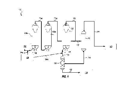
implementations,
the data processing unit 124 can interface with other devices using a wired
connection via the I/0
.. unit 123. The data processing unit 120 can also interface with other
external interfaces, sources
of data storage, and/or visual or audio display devices, etc. to retrieve and
transfer data and
information that can be processed by the processor 121, stored in the memory
122, or exhibited
on an output unit of the mobile device 130 (e.g., smartphone) or an external
device.
[0077]
The wearable, non-intrusive microneedle sensor patch device 100 provides a two-
component wearable sensor system (e.g., disposable sensor and reusable
electronics) that
addresses multiple, multi-faceted problems of current state-of-the-art
microneedle sensor
systems. For example, the specially-designed spiked microneedle structures of
the wearable,
non-intrusive microneedle sensor patch device 100 is configured to have a
geometry, length and
girth (e.g., aspect ratio), surface roughness, and material configured to not
cause substantial pain
to the user, while still having the necessary detection sensitivity of a
conventional electrode to
meet the requirements of an electrochemical electrode system, such as (i)
allowing chemically-
functionalization to facilitate redox or other chemical reactions with a
target analyte in the host
biofluid, (ii) conducting electrical signals produced from such reactions with
the target analyte to
detect parameters (e.g., concentration) of the target analyte in the biofluid,
and (iii)
reproducibility and reliability of the detectable electrical signals.
[0078]
For example, the spiked microneedle structures 111, in contrast with
conventional
18
CA 03226577 2024-01-05
WO 2023/283385
PCT/US2022/036424
photolithography-based silicon microneedle structures and other existing
microneedles, can be
manufactured in a wide range of geometries made appropriate to specific skin
penetrating
applications and using a wide range of materials, e.g., including most
polymers, metals such as
aluminum and some classes of steels, and also some ceramics and semiconducting
materials.
Moreover, the spiked microneedle structures 111 can be structured to have a
unique and high
surface roughness (e.g., in a range of 50 nm to 400 nm peak roughness, such as
for PMMA
spiked microneedle structures fabricated by the disclosed micro-computer
numerical control
(CNC) or micro-molding techniques), which is highly desired for sensing
applications enabling
enhanced sensitivity as well as reagent protection and overall enhanced
structural integrity of the
reagent layers¨each of which contributes to long term stability of the sensor.
[0079] Additionally, for some embodiments of the disclosed spiked
microneedle structures
111 (discussed below), the body of the microneedle can include a unique spiral
structure, in
contrast with conventional flat microneedle body structure, which enhances the
applied
penetration stress by turning the single shear stress in a non-spiral
structure to added shear and
torsional stresses, e.g., resulting in reduction of the penetration force
required to move through
the skin, and thus reduction of potential pain as well as potential trauma to
the skin of the wearer.
[0080] Moreover, for example, the wearable, non-intrusive microneedle
sensor patch device
100 is configured to space the spiked microneedle structures on the substrate
to mitigate or
eliminate 'cross-talk' that typically plagues a multi-analyte detection
sensor. For example,
multi-analyte sensors for detecting oxidase-based enzymes, in particular, can
suffer from
chemical cross-talk that largely affects the detectable signal response and
thus accuracy of the
multiplexed sensors. The chemical cross-talk is a result of the diffusion of
the hydrogen
peroxide enzymatic product of an analyte sensor to a neighboring sensor for
another analyte. In
the example embodiments disclosed herein, the cross-talk issue can be
addressed through a
combination of optimizing the spacing between the microneedle sensors and
mitigating the
amount of chemical agents susceptible to cross-talk (i.e., mitigated
sensitivity). In some example
embodiments, the sensitivities can be reduced in multiplexed sensors via
reducing the number of
microneedles (i.e., reducing the active surface areas) to below 10 nA.mM-1,
and/or the spacing
can be kept above 5 mm to remove any chemical cross-talk possibility.
[0081] Further advantages of the disclosed microneedle sensor technology
include
robustness of the overall sensor patch device. For example, the wearable, non-
intrusive
19
CA 03226577 2024-01-05
WO 2023/283385
PCT/US2022/036424
microneedle sensor patch device 100 can be structured to safely secure the
spiked microneedle
structures 111 to the sensor substrate 113 by providing a sealed base
structure 115 that surrounds
the lower portion of the spiked microneedles 111, which can be fabricated by a
new fabrication
technique in accordance with the disclosed technology that is scalable, mask-
free, and
reproducible to create this stabilizing, insulation layer for the array of
spiked microneedles 111.
[0082] FIGS. 2A and 2B show images and diagrams showing various aspects
of an example
embodiment of the spiked microneedles 111. The images and diagrams in FIG. 2A
demonstrate
the geometry of the spiked microneedle structures 111 and their securement to
the substrate 113
via the sealed base structures 115. SEM image 201 shows example spiked
microneedles 111 on
substrate 113 prior to the sealed base structure 115 added; diagram 202 shows
an example spiked
microneedle tip depicting an example of the tip dimensions (e.g., tip angle of
80 , tip height of
119 [tm, and tip base of 200 [tm diameter length, with tip aspect ratio of -
=0.6, height:base); and
diagrams 203 and 204 show example embodiments of a spiked microneedle 111 with
a sealed
base structure 115 of different heights (e.g., 250 [tm height and 250 [tm
diameter length in
.. diagram 203, and 450 [tm height and 350 [tm diameter length in diagram
204).
[0083] In some embodiments of the wearable, non-intrusive microneedle
sensor patch device
100, for example, the spiked microneedle structures 111 can be configured to
have a height
(from body base to tip apex) in a range of 800 [tm to 4,000 [tm (0.8 mm to 4
mm). In some
embodiments, for example, the tip of the spiked microneedle structures 111 can
be configured to
have: (i) tip height in a range of 100 [tm to 200 [tm, (ii) tip base diameter
or thickness in a range
of 50 [tm to 450 [tm, and (iii) tip angle (at apex to tip base) in a range of
40 to 85 . In some
embodiments, for example, the body of the spiked microneedle structures 111
can be configured
to have a diameter or thickness (e.g., horizontal length or girth) in a range
of 50 [tm to 450 [tm.
In some embodiments, for example, the spiked microneedle structures 111 can be
configured to
have an overall height-to-thickness aspect ratio in a range of 4:1 to 20:1.
[0084] Also, as shown in FIG. 2A, the spiked microneedle structures 111
are designed in a
specialized non-intrusive, pain-free skin-penetrating geometry, also referred
to as "reproducibly
randomized spiral (RRS)," which includes a circular cross-section having a
thin, winding spiral
protrusion (spiral structure 112) that is extruded from a solid surface base
to a desired height at
the tip of the spiked microneedle. The spiked microneedle structures 111 are
configured to have
their circular body spirally span from the microneedle structure base (bottom)
to a point along
CA 03226577 2024-01-05
WO 2023/283385
PCT/US2022/036424
the body that defines a base of the tip, from which the microneedle structure
converges to a sharp
point at the apex.
[0085] FIG. 2B shows another SEM image depicting an example tip region
of an example
spiked microneedle structure 111 and an illustration of an example spiked
microneedle structure
111 having the spiral structure 112. As depicted in the SEM diagram 201 shown
in FIG. 2A and
the illustration shown in FIG. 2B, the body (and outer wall) of the spiked
microneedle structure
111 is configured to be spiral-like with a spiral structure 112, which can
have at least 20 of
spiral angle and at least 25 [tm of valley-to-spike height. This structure,
for example, can
enhance the skin penetration by introducing added torsional stresses of the
spiked microneedles
111 at a constant pressure, e.g., as compared to the flat, non-spiral surface
of a microneedle
body, while pressing the microneedle patch to the skin, which result in a
smoother skin
penetration. Additionally, the spiral structure 112 of the body (and outer
wall) of the spiked
microneedle structure 111 reduces the surface contact (friction between the
two bodies) at the
microneedle/skin interface, e.g., thus reducing the insertion force required.
This reduction in
surface force not only reduces the potential for pain to the user, but also
reduces deleterious
forces that can damage the microneedles and/or the skin tissue with consequent
traumatic bodily
reactions, thereby providing the overall sensor unit 110 with more robust,
stable spiked
microneedle structures 111, and sensing capability.
[0086] This disclosure provides example comparative data of example
embodiments of the
wearable, non-intrusive microneedle sensor patch device 100 and conventional
microneedle
sensors, demonstrating how end users of the example spiked microneedle sensor
device 100
experienced little or no pain (e.g., pain level of 0, 1 or 2 on a scale of 1-
10), whereas end users of
conventional microneedle sensor devices experienced significant pain (e.g.,
pain level of 4 to 8
on the scale of 1-10).
[0087] Table 1 shows example data from a qualitative pain study using an
example
embodiment of the disclosed spiked microneedle sensor patch device, e.g.,
including the spiral-
winding projection on the extending body of the microneedle, e.g., in
comparison with different
conventional microneedle sensor devices on human subjects with different ages,
ethnicity, and
gender.
21
CA 03226577 2024-01-05
WO 2023/283385
PCT/US2022/036424
Table 1
WON:
IPONMEMONVIKWAttOMMEMECNNOMMOPOOMENEMMAIRMIONakIMEMENEM
1 1/10 5/1() 6,110
7110
6/lo
:1 /10.. Sl:10 ====
0110 4/10 6/10
0/10: 6/10
7 0/10 4110 6110
[0088] In some embodiments, for example, on the sensor substrate 113,
the spacing among
spiked microneedle structures 111 can be configured to be at least 1.3 mm
apart from each other.
5 .. Also, for example, in cases for multiple (multiplexed) analyte sensors,
the spacing between
different sensing electrode regions (e.g., glucose, lactate, alcohol etc.) can
be configured to be at
a least 5 mm.
[0089] In some embodiments, for example, the spiked microneedles 111 are
structured to
include a rigid, insulative material core that is coated by an electrically
conductive material, such
that a detectable electrical signal at the tip of the spiked microneedle
(operating as an electrode)
is conducted along the electrically conductive outer coating to an electrical
conduit disposed in
or on the substrate 113. For example, in some embodiments, the core or
interior material of a
spiked microneedle structure 111 includes one or more polymeric materials,
e.g., including but
not limited to poly(methyl methacrylate) (PMMA) polyether ether ketone (PEEK),
polycarbonate (PC), ultra-high-molecular-weight polyethylene (UHMW), and/or
photocurable
copolymer(s), which can be obtained from urethane dimethacrylate,
bisphenylglycidyl
dimethacrylate, and triethylene glycol dimethacrylate; and in some
embodiments, for example,
the electrically conductive outer coating includes, but is not limited to, one
or more of gold,
platinum, silver, chromium, a carbon material (e.g., graphite, boron-doped
diamond, highly
.. oriented pyrolytic graphite, graphene, carbon nanotubes (CNTs), or other
carbon material) and/or
other conductive metal or alloy. For example, a first set of spiked
microneedle structures can be
configured to include a first electrically-conductive outer coating (e.g.,
platinum, gold, silver,
22
CA 03226577 2024-01-05
WO 2023/283385
PCT/US2022/036424
etc.) for the detection of a first target analyte, and a second set of spiked
microneedle structures
can be configured to include a second electrically-conductive outer
coating(e.g., graphite carbon,
B-doped diamond, etc.) for the detection of a second (other) target analyte
present in the biofluid.
In some embodiments, for example, a thin-film deposition of the electrically
conductive material
includes sputtering Cr/Pt/Ag, followed by etching of Ag from all at least one
or some of the
spiked microneedles 111 of the array (e.g., etching of Ag on the spiked
microneedles configured
to be working and counter microneedle microelectrodes), and then followed by
chloritization of
the Ag to Ag-AgC1 on at least one or some of the spiked microneedles 111 of
the array (e.g.,
configured to be the reference microneedle microelectrode(s)). The reference
microneedle
electrodes can be further coated by a first reference electrode coating (e.g.,
a NaCl-saturated
solid polymer matrix), which can be subsequently coated by a second reference
electrode coating
(e.g., an outer PVC polymer containing Triton X-100 surfactant).
[0090] FIG. 3 shows panels of images and diagrams showing the
microneedle sensor unit
110, including an example arrangement of the spiked microneedles 111 on the
substrate 113 and
substructure of the substrate 113. On the left side of FIG. 3, image 301 shows
an example single
(left) and multiple (right) analyte sensor unit, respectively; image 302 shows
an optical
micrograph of an example spiked microneedle array with 150 p.m diameter next
to a stainless-
steel insulin injection nano-pen (34 gauge); and SEM images 303 show zoomed
views of an
example spiral spiked microneedle 111. On the right side of FIG. 3, a top
series of diagrams
illustrates an example array of spiked microneedles 111 on the substrate 113
with an example
network of microfluidic channels 117 (which can be used to flow insulative
material to seal the
spiked microneedles 111 and form a sealed base 115), as well as show how this
combines with
an example cover unit 119 to form an example sensor unit 110. A middle series
of diagrams
illustrates a side view of the example cover unit 119, configured as a ring
cover 319. The lower
series of diagrams illustrate an example embodiment of a spiked microneedle
sensor unit 310 for
multi-analyte simultaneous detection, which includes two sensor regions of
spiked microneedles
(each with 1.7 mm spacing between spiked microneedles), a reference electrode
(e.g., Ag-AgC1),
a counter electrode (e.g., Pt), and electronic-connection holes. The lower
series of diagrams also
includes images showing individual spiked microneedles on a single strand of
hair and their
penetration to the skin (e.g., on a finger).
[0091] FIG. 4A shows illustrative diagrams showing various aspects of an
example spiked
23
CA 03226577 2024-01-05
WO 2023/283385
PCT/US2022/036424
microneedle sensor unit 110, including example spiked microneedle structures
111 and base
structures 115 and example array configurations. On the left side of FIG. 4A,
a diagram 401
shows an example embodiment of a spiked microneedle 111 with an insulated
sealed base
structure 115 and network of microfluidic channels 117, within which a
sealant/insulator
material can flow through to create the sealed base structure 115. Diagram 402
of FIG. 4A
shows example 5x5 array of spiked microneedle structures 111 on a substrate
113 featuring
various substructures of differing networks of microfluidic channels 117,
e.g., including a
"chess-like" microfluidic channel structure 417A that encompasses each spiked
microneedle
structure 111, a "regional" microfluidic channel structure 417B that
encompasses sensor regions,
and a "multi-sense" or "dual-sense" microfluidic channel structure 417C that
encompasses
particular sensor regions associated with multiple (or dual) analyte sensing.
Diagram 403
illustrates an example assembly process to insert an example cover unit 119
(e.g., ring cover 419)
on an example spiked microneedle sensor array-substrate (e.g., spiked
microneedle array
substrate 414) to produce an example embodiment of the microneedle sensor unit
410. Notably,
in this example, the sealed base structures that surround and support the base
region of the spiked
microneedles to the substrate are produced after insertion of the ring cover
419 to the spiked
microneedle array substrate 414, e.g., by microfluidic transfer and sealing of
a resin material, as
discussed below.
[0092] For example, in some implementations, the spiked microneedle
array-substrate (e.g.,
spiked microneedle array substrate 414) and the cover unit (e.g., ring cover
419) are sealed
together using a new technique that utilizes a network of microfluidic
channels that are engraved
in the substructure of the sensor substrate. The network of microfluidic
channels are responsible
for flowing a custom-made resin with optimal viscosity and capillary
properties from a single-
entry point through the entire network of microchannels to the cover unit /
microneedle array-
substrate interface, which can flow up to a cut-off fluidic line that is
designed to stop the
capillary flow of the resin-based sealant/insulator at the line. This
technique is referred to as an
autonomous capillary sealing/insulating method, which both seals the two
components (i.e., the
spiked microneedle array-substrate and the cover unit) and insulates each of
the spiked
microneedles in a highly reproducible manner at the cut-off fluidic line
stopper. The method can
fabricate the sealed base structures at, at least, tens of microns to hundreds
of microns high (e.g.,
250 [tm or 450 [tm as shown in FIG. 2A), during which a
reproducibility/capillary cutoff line of
24
CA 03226577 2024-01-05
WO 2023/283385
PCT/US2022/036424
the substructure of the substrate 113 can stop capillary motion of the resin-
based
sealant/insulating fluidic polymer that seals the two components (cover unit
and spiked
microstructure components) together creates the insulating structure of the
base structure 115
surrounding the desired lower portion of the bare spiked microneedle
electrodes surface area.
[0093] FIG. 4B shows a cross-sectional view diagram 407 illustrating an
example
embodiment of spiked microneedle structures 411 and substructure of substrate
413 (e.g., of
PMNIA material, or other polymer, metal and/or ceramic material) with an
example network of
microfluidic channels 417 and covered by an example ring cover 419, which
facilitate the
autonomous capillary sealing/insulating method that can flow the custom resin
material 418
through the microfluidic channels 417 and through gaps between the
substructure 413 and cover
419 and outward to the cut-off line 421, which can create sealed base
structures (e.g., via
photocuring the resin 418). In example implementations of the method, for
example, the cut-off
line 421 or area of the spiked microneedle structure 411 can (i) provide a
location where the
autonomous flow of the microfluidic sealant stops flowing, and (ii) serve as a
structure
responsible for where the spiked microneedle structures are to be reproducibly
insulated.
[0094] FIG. 4C shows cross-sectional view diagrams 451 and 452
illustrating example
embodiments of spiked microneedle structures 411 and substructure of substrate
413 with an
example electrical conduit 412 that is configured to electrically couple the
electrode 411E of the
spiked microneedle structure 411 to a terminus or contact region of the
electrical conduit 412 on
the substrate 413 (not shown). The diagram 451 depicts an example embodiment
where the
electrical conduit 412 is configured on or at least partially in the substrate
413; and the diagram
452 depicts an example embodiment where the electrical conduit 412 is
configured within the
substrate 413. In these examples, the s substrate 413 is covered by the
example cover 419.
[0095] Referring back to diagram 403 in FIG. 4A, the autonomous
capillary
sealing/insulating method is a spontaneously autonomous process that includes
(1) a process 431
to assemble the cover unit and microneedle array-substrate, followed by
multiple processes 433
involving (2a) contact and inflow of the custom-designed photocurable resin
from the contact
side of the assembled sensor patch through the network of microfluidic
channels, (2b) followed
by heat treatment (e.g., at 70 C for 5 minutes), (2c) followed by UV curing
(e.g., at 90 C for 1
hour). The resulting device, e.g., spiked microneedle sensor unit 410, is a
single component
sensor array fully sealed and reproducibly insulated. Notably, the resulting
sensor unit (e.g.,
CA 03226577 2024-01-05
WO 2023/283385
PCT/US2022/036424
single piece) becomes significantly tough with greatly enhanced mechanical
robustness, which
can be attributed, for example, due to the specialized resin filling the
vacant microfluidic
channels and/or inner micro-gaps between the cover unit (e.g., cover ring 419)
and the
substructure, and around the holes of the cover ring 419 and the individual
spiked microneedles,
e.g., based on the mechanically tough properties of the resin material.
[0096] Also, for example, the microfluidic channels (e.g., which can
have a depth and/or
width ranging from 100-400 p.m) that are created on and/or in the substructure
can also serve as
electrical isolation channels (e.g., when masked or engraved to individually
addressable
electrical regions) for an electrical isolation process step of the
fabrication method, which can
include (i) guiding the mechanical scraping of the metal sputtered inside the
channels (that can
leave the rest of the substrate into electrically isolated islands / regions),
or (ii) holding solid or
liquid-based masks that can be fit inside the channels before any metal
deposition and removed
after the metal thin film deposition. This can be implemented by laser
engraving, micro-CNC
machining, or manual scraping of the metal inside of the channel according to
the final design of
the spiked microneedle regions, as illustrated by the examples in diagram 402,
which can leave
certain regions to be electrically connected or electrically isolated from
each other. Further
details about the fabrication method are described later in this patent
document.
[0097] FIG. 5 shows diagrams depicting example embodiments of the
substructure of the
microneedle sensor unit 110 and electrical interface 126 of the electronics
unit 120, showing how
the electronic interface contact is designed for reliability of electrical
signal transfer across
electrical contacts from the sensor unit 110 (e.g., disposable component) to
the electronics unit
120 (e.g., signal conditioning unit, which can provide a potentiostat). The
substrate 113 includes
a plurality of electrically-conductive, friction-based contacts 510 (e.g.,
less than 100 nm
thickness) that are disposed within openings 512 of the substructure of the
substrate 113. The
example electrically-conductive, friction-based contacts 510 are coupled to
electrically-
conductive conduits (e.g., interconnects or vias) that couple to the array of
electrodes of spiked
microneedle structures 111. The example openings 512 of the substructure of
the substrate 113,
combined with the electrically-conductive, fiction-based contacts 510, are
sized to receive the
elongated region of rigid electrically-conductive pin structures 526 of the
electrical interface 126.
[0098] For example, an advantage of the sensor/electronics electrical
interface design is
related to the single-step sputtering/metal film deposition process of the
microneedle sensor unit
26
CA 03226577 2024-01-05
WO 2023/283385
PCT/US2022/036424
110, which allows for top-down sputtering that fills the openings 512 with
electrically
conductive material to form the contacts 510, where the rigid conductive pins
526 of the
electronics unit 120 (or an intermediate interface) inserts. The resulting
electrically-conductive,
friction-based contact 510 provides an electrical-noise-free and reliable
interface, even during
high intensity body motions (by the user), which is a challenging objective to
achieve (e.g.,
particularly for nano-ampere sensitivity systems for epidermal analyte-based
electrochemical
sensing applications). The rigid, electrically-conductive pin structures 526
are configured on the
PCB layer of the electronic unit 120 to mechanically align with corresponding
openings 512.
Such pin structures 526 can be fabricated using an orientation aligner design
and configured to
have a round tip at the apex of the pin structure 526 for smooth insertion to
the openings 512 of
the sensor unit 110. Also, for example, the bottom side of the contacts 510
within the openings
512 can be designed and fabricated to be beveled to provide a wider entrance
zone for easier
guiding of the rigid pins 526 into the openings 512.
[0099] FIG. 6 shows a diagram depicting a multiplexed sensor design for
measuring specific
analyte parameters in continuous monitoring of glucose/lactate and
glucose/alcohol. Example
implementations were performed using an example sensor like that in FIG. 6,
which
demonstrated a cross-talk-free wearable microneedle sensor patch device
capable of
simultaneous, multiplexed sensing of multiple subdermal analytes with spiked
microneedle
structures on a substructure with spacing (between target analyte 1 and target
analyte 2 sensor
regions) of at least 5 mm. For example, the example spiked microneedle sensor
patch device as
configured to provide two working electrode sensor regions with identical
detection mechanisms,
such as oxidase-based sensors (which rely on H202 as the sensing molecule).
The sensor patch
device was able to provide a mitigated sensor sensitivity range of at most 10
nA/mM for each
sensing region. The sensor patch device was also configured for use of common
or an
individually addressable auxiliary/counter electrode(s), and for use of common
or an individually
addressable reference electrode(s). Also, in these example implementations, a
sealing cover with
at least two embedded non-intrusive skin insertion enhancing rings or ring-
like elevated surfaces
was used. Glucose-Lactate continuous measurements were demonstrated, along
with Glucose-
Alcohol continuous monitoring. Example results and techniques in these example
implementations are discussed later in this patent document, in detail. It is
notable that this
example multiplexed design/strategy can be readily generalized and expanded
for more than two
27
CA 03226577 2024-01-05
WO 2023/283385
PCT/US2022/036424
target analytes and to any type of biomarkers such as metabolites,
electrolytes, drugs, hormones,
proteins, and oligonucleotides.
[00100] FIG. 7 shows images illustrating interim and final components produced
by an
example implementation of a micro-CNC fabrication method in accordance with
the present
technology. Image 701 shows a CNC-fabricated array of spiked microneedle
structures on a
substrate. Image 702 shows a polydimethylsiloxane (PDMS) negative of the array
in image 701.
Images 703a and 703b show a replica of the spiked microneedle array in image
701, which was
fabricated using micro-casting. SEM image 704 shows a zoomed view of the tip
of a spiked
microneedle structure in images 703a, 703b, and SEM images 705 and 706 show
ultra-zoomed
views of the spiked microneedle structure, which demonstrates the nanoscale or
microscale
roughness (e.g., 500 nm - 5 [tm) of the CNC-fabricated spiked microneedle
structure surface, as
well as the nanoscale precision of the method.
[00101] The example spiked microneedle arrays shown in FIG. 7 were implemented
by non-
adhesive, micro-casting, micromachining, injection molding, ultra-high
resolution 3D printing,
and/or precision drawing microneedle fabrication method using polymer-based
materials, in
accordance with the present technology. The fabrication method is a highly
scalable,
inexpensive, and highly reproducible micro-casting technique for manufacturing
spiked
microstructure arrays. In this method, a non-adhesive polydimethylsiloxane
(PDMS) negative of
a spiked microstructure array is prepared utilizing a micro-computer numerical
control (micro-
CNC) method to create a PMMA block, e.g., using the developed strategy,
tooling and
machining sequence. Next, a custom-developed, biocompatible, FDA grade, photo-
curable resin
is poured into the PDMS negative to form the final spiked microstructure
array, followed with
multiple post processing steps.
[00102] Notably, in the course of refining this technique, there were a few
key parameters
regarding the post-processing of the photo-curable resin polymer that were
found to solve the
common problems of low-temperature casting methods. For example, these
problems include
the incomplete filling of the resin, low resolution and lack of forming a
nanoscale surface
roughness, usual adhesion problems between the mold and the final
microstructure, lack of tip
sharpness, gas bubble formation and other issues¨all of which are successfully
addressed by the
use of the newly developed polymeric photocurable resin with optimal
characteristic, as well as
manufacturing process parameters tailored to the custom-made resin.
28
CA 03226577 2024-01-05
WO 2023/283385
PCT/US2022/036424
[00103] In some embodiments of the polymeric photocurable resin material, for
example, the
resin was prepared to an optimal viscosity by addition of nonionic surfactant
(e.g., Triton X-100,
in a concentration range of 0.1-1 wt%) to a biocompatible polymer, which
included a
biomedical-grade photocurable polymer resin. The surfactant additive, along
with thermal
treatment of the polymer mixture (e.g., at 65 C for 20 min), resulted in
enhancing the
flowability (e.g., by reducing viscosity and enhancing surface energy) of the
resin and led to
nanoscale resolution of the method, without affecting the photo-crosslinking
process and
mechanical robustness of the finished material.
[00104] Notably, using the polymeric photocurable resin material in the
fabrication method,
the final manufactured spiked microneedle structures showed excellent solvent
compatibility
against both organic and inorganic harsh solutions, such as acetone,
isooctane, ethanol, bleach,
concentrated NaOH and HC1 solution, hydrogen peroxide (3%) and saline water
(3.5% NaCl),
even up to 24 hours. Furthermore, manufactured spiked microneedle structures
have
demonstrated a remarkable compatibility to sterilization methods (e.g., Gamma
radiation,
ethylene oxide, autoclave treatments up to 125 C for an hour, or UVc
treatment). The disclosed
fabrication method identified manufacturing process parameters that mitigate
various problems,
like incomplete filling, bubble formation, and low resolution, by combined use
of the customized
low-viscosity resin material, vacuumed pouring of the custom resin at an
elevated temperature
(e.g., 70 C for 6 hours) followed by UV curing (e.g., 90 C UV curing for 90
minutes). The
example results produced a Nanometer-precision replica with superior
mechanical fracture
toughness, e.g., with <5 microns of tip sharpness as shown in FIG. 7.
[00105] Several example implementations are described below that demonstrate
example
embodiments of the wearable, non-intrusive microneedle sensor technology
providing unique
advantages based on the structural design, functional achievements, and unique
methods and
materials for fabrication and functionalization layer immobilization, while
keeping the highest
level of biocompatibility, mechanical robustness, reproducibility
requirements, sensor sensitivity
and selectivity requirements, and longevity for continuous analyte (or multi-
analyte) on-body
sensing.
[00106] Example Implementations with Continuous, Real-Time Monitoring of
Single
and Multiple Analytes Including Glucose, Lactate, and Alcohol via a Fully
Integrated
Wearable Microneedle Platform
29
CA 03226577 2024-01-05
WO 2023/283385
PCT/US2022/036424
[00107] Wearable sensors capable of monitoring biochemical markers are poised
to help
enable a new revolution in personalized healthcare, telehealth, and early
disease diagnosis.
Among potential biomolecular sampling biofluids accessible via wearable
sensors, interstitial
fluid (ISF) has the closest composition to the blood, with temporal profiles
of most analytes
approaching those observed in blood. In addition, direct ISF measurements are
not affected by
major issues common to other biofluids such as long lag times, variable
secretion rates, sample
contamination and dilution, and most importantly limited correlation, all of
which greatly limit
the sensor's clinical utility. Microneedle (MN)-based sensing technologies
provide pain-free,
and non-intrusive continuous access to constantly revitalizing ISF.
.. [00108] In the discussion below, presented are example embodiments of a
fully-integrated,
non-intrusive, and wearable microneedle sensor platform that includes reusable
and disposable
contingents and utilizes a biocompatible array of microneedles fabricated via
an advanced micro-
machining technique. The disclosed microneedle sensor platform is optimized
for real-time,
continuous, and multiplexed biomolecular measurements on freely behaving human
subjects.
.. This platform addresses multifaceted challenges in the areas of system
integration, fabrication,
packaging, biocompatibility and sterilization, skin penetration, sensitivity
and stability, and low-
power yet real-time biosensing in an inexpensive manner.
[00109] In example implementations of some embodiments of a fully-integrated,
non-
intrusive, wearable microneedle sensor array device, which includes two
components of a
.. reusable electronics and a disposable sensor, the device showed remarkable
ability in tracking
the dynamic profiles of key metabolites (e.g., lactate, glucose, and alcohol)
during common daily
activities via a small, wireless-enabled wearable, with results well
correlated to gold-standard
metrics. The multiplexed sensing potential of the platform is also
demonstrated through
simultaneous on-body monitoring of lactate-glucose and alcohol-glucose, along
with the
.. demonstration of a custom designed smartphone app for data capture and
visualization. The
example system is believed to mark a major new milestone for continuous, real-
time, and
accurate monitoring of clinically relevant biomolecules, and presents a major
leap forward for
next-generation wearable health monitors.
[00110] By nature of being attached to the body, wearable sensors offer the
ability to
.. continuously monitor physiological parameters in real-time on freely
behaving subjects,
providing interesting new insights into human health and wellness not offered
by spot
CA 03226577 2024-01-05
WO 2023/283385
PCT/US2022/036424
measurements taken in the clinic or by point-of-care devices. Merging wearable
sensors with
rapidly growing "omics" technologies, internet of things (IoT) devices, and
artificial intelligence
(AI), can potentially offer revolutionary advances in personalized healthcare,
early disease
detection, telemedicine/remote monitoring, personalized nutrition or wellness,
or even detection
of symptoms associated with COVID-19 or other viral infections.
[00111] Yet, most commercial wearables monitor only a handful of physical
parameters, such
as heart rate and motion, which offer only generic physiological insights. To
address this issue,
recent efforts have shifted to wearable devices that can detect in real time
molecular markers on
the skin surface through electrochemical analysis. State-of-the-art, non-
invasive chemical sensor
research has mainly revolved around epidermal sensors utilizing stimulated
sweat or extracted
interstitial fluid (ISF). However, both these skin-worn sensors still face
significant challenges,
including how to continuously access to the biofluid (e.g., via exercise or
electrical stimulation),
fluctuating flow rates, varying parameters (e.g., sweat pH, salinity, and
temperature), sample
mixing, carry-over, dilution, or contamination. These challenges, along with
the limited
correlation of some sweat biomarkers to gold-standard blood assays, and
significant lag time,
require considerable research efforts towards making these epidermal platforms
clinically viable.
[00112] Instead of analyzing biochemical markers on the surface of the skin,
analysis under
the skin¨directly in ISF¨provides a well-established, high degree of
correlation with blood for
many biomarkers of interest. In fact, continuous glucose monitors (CGMs),
approved for use by
the US Food and Drug Administration (FDA) for diabetes management, sense
glucose in ISF
with excellent correlation to blood. However, current CGMs presently rely on
invasive needle-
based sensors, and are limited to measuring only a single analyte.
[00113] In contrast, microneedle (MN) technology, hailed recently by
Scientific American
and the World Economic Forum as the top emerging technology for shaping the
future of
healthcare, utilizes micron-sized needles that penetrate the skin by only a
few hundred microns
to offer a pain- and discomfort-free way of accessing ISF, obviating the need
for 5-11 mm long
needles common to CGMs. In addition, the limited single-analyte sensing
capability of current
CGM devices is readily addressable in MN platforms by utilizing multiple
individually-
addressable spatially-isolated sensing electrodes on a single platform, which
allows for
significant new detection opportunities. The micron-scale nature of the MN
sensors allows for
their application on multiple locations on the body, making it adaptable to
different form factors
31
CA 03226577 2024-01-05
WO 2023/283385
PCT/US2022/036424
such as rings, and epidermal patches. Despite the tremendous opportunities
offered by MNs, the
realization of their full potential for practical wearable chemical sensing
has remained an unmet
challenge, reflecting primarily the multidisciplinary nature of these
challenges that calls for a
holistic approach in reliably addressing them.
[00114] As described below, an example of a fully integrated, wirelessly-
operated spiked
microneedle platform for continuous monitoring of ISF biomarkers is
demonstrated on human
subjects. Example embodiments and implementations are described illustrating
the present
example of the disclosed microneedle sensor device technology.
[00115] FIG. 8 shows a diagram of an example embodiment of a fully-integrated,
non-
intrusive, wirelessly-operated, wearable microneedle sensor platform in
accordance with the
example embodiment of the wearable, non-intrusive microneedle sensor patch
device 100 shown
in FIGS. 1B-1D. As shown in FIG. 8 (left panel (a)), a skin-wearable sensor
system can include
the wearable, non-intrusive microneedle sensor patch device 100 that
continuously collects rich
molecular data to facilitate greater understanding of the body's response to
daily activities. Real-
time monitoring of ISF biomarkers (e.g., glucose, lactate, alcohol, ketone
bodies, sodium, and
other analytes) is achievable, with glucose, lactate, and alcohol demonstrated
in example
implementations for both individually (single analyte) and simultaneously
(multiplexed), with
results well correlated to those of the corresponding gold standard (blood or
breath)
measurements over a prolonged duration. To achieve this, multifaceted
challenges in the areas
of system integration (e.g., sensor, electronics, firmware, and mobile app
development),
fabrication, skin penetration, and stable, accurate, and cross-talk-free
biosensing, are successfully
addressed through a holistic approach which is elaborated below.
[00116] As illustrated in FIG. 8, a fully integrated spiked microneedle sensor
system, which
can include an array of multiple sensors and custom electronics, was designed,
fabricated,
.. developed, and tested. The integrated system can include distinct sub-
components (e.g., shown
previously in FIG. 1C), which are assembled into two primary
components¨disposable sensor
component 110C and reusable electronics unit 120C. Right-side panel (d) of
FIG. 8 shows
multiple schematics and images depicting how the example device 100 allows for
convenient
replacement of the low-cost disposable sensor component 110C according to its
functional life.
Molecular level electrochemical signals from the wearer's ISF are continuously
and selectively
gathered by the epidermis-inserted spiked microneedle tips (FIG. 8, panel
(dill), showing an SEM
32
CA 03226577 2024-01-05
WO 2023/283385
PCT/US2022/036424
(scale bar: 75 p.m) of a tip structure of a spiked microneedle), which the
signals are carried
through the low-noise, reusable sensor-electronics (reusable electronics unit
120C) through a
physical interface between disposable sensor component 110C and reusable
electronics unit
120C, and which can be wirelessly transmitted to the mobile device 130 for
remote data
.. processing, e.g., via a software application (app) executable on the mobile
device 130 (FIG. 1A
and FIG. 8, panel (dii)), e.g., for visualization and analysis of the real-
time monitoring of
analytes. The entire operation can be wirelessly controlled by the
accompanying app.
[00117] FIGS. 9-11 show schematics and images depicting an example embodiment
of the
disposable sensor component 110C and the reusable electronics unit 120C shown
in FIG. 8, e.g.,
used in the example implementations. FIG. 9 shows schematic diagrams
illustrating the example
electronics and sensor architecture for the disposable sensor component 110C
and the reusable
electronics unit 120C, labeled 920C in FIG. 9, where panel (ai) shows a
functional block diagram
of example components in an architectural configuration of the reusable
electronics unit 120C;
panel (au) shows an abridged functional block diagram of an example AD5940
electrochemical
AFE (recreated from the component's datasheet); panel (aiii) shows an image
depicting an
example of the electronic system PCB connection to a battery (e.g., through a
low-profile
connector) and to the charging coil (e.g., through large solder pads); and
panel (aiv) shows a
diagram showing example components of the reusable electronics unit 120C,
including example
electronic interface connection pins 911 and a break-out diagram 912
demonstrating how the
disposable electronic unit 120C interfaces to the disposable sensor component
110C (i.e., spiked
microneedle array 171) via the connection pins 911¨which, in this example,
insert into
conductive holes ("E-connection Hole" in the diagram 912) on the sensor base
(e.g., where such
holes can be made conductive by sputter deposited metal within CNC milled
holes), and where
mechanical guides at the base of the conductive pins 911 provide mechanical
retention to the
example electronic system PCB. FIG. 10 shows illustrations of an example
individual
microneedle (with corresponding dimensions for the particular example) in
panel (bi), a side-
view depiction of an example embodiment of the disposable sensor component
110C and
reusable electronics unit 120C in panel (bii), and a perspective-view
depiction of an example
multiplexed spiked microneedle sensor with microneedle groups configured as
two separated
working electrode arrays with corresponding counter and reference electrodes,
in panel (biii).
The example shown in FIG. 10 panel (bi) shows a spiked microneedle with a bare
extending
33
CA 03226577 2024-01-05
WO 2023/283385
PCT/US2022/036424
body; whereas in other examples (such as FIG. 2A), the spiked microneedle can
include a
winding protrusion (also referred to as a winding projection), such as the
example winding spiral
protrusion 112 in FIG. 2A. FIG. 11 shows SEM images showing side- and top-view
of an
individual microneedle tip (scale bar of 100 p.m) in panels (ci) and (cii), a
SEM image of multiple
microneedles (scale bar of 500 p.m) in panels (ciii), images of a batch of
four micromachined
spiked microneedle arrays before after sputtering of thin film metals (scale
bar: 2.5 cm and 2 cm,
respectively) in panels (civ) and (c,), and images of an assembled microneedle-
cover ring for
single and multiple sensing, respectively (scale bar of 1 cm) in in panels
(cvi) and (cvii).
[00118] The schematics and images in FIGS. 9-11 demonstrate an example
embodiment of
the disclosed wearable, non-intrusive microneedle sensor patch device 100,
designed for
functionality, compactness, and low power operation. For example, to acquire
electrochemical
signal data and subsequently transmit it, the example reusable electronic unit
920 of the device in
FIGS. 9-11 utilizes two integrated circuits: an electrochemical analog front
end (AFE) and a
Bluetooth Low Energy (BLE) system-in-package (SiP). In this example, the AFE
provides the
circuitry for multiplexing between up to four independent working electrodes,
signal
conditioning (amplification and filtering), and signal digitization, while the
BLE SiP provides a
low power microcontroller for processing the digitized signals, as well as a
BLE radio and
embedded antenna for data transmission. Powering these components, in this
example, is
accomplished by a lithium-polymer battery (through a voltage regulator), which
is inductively
charged through a wireless charging IC and charging coil (e.g., see FIG. 15).
Additionally,
power optimizations for the AFE and BLE SiP enable ¨30 days of battery life
while maintaining
a relatively small battery size (e.g., see FIG. 16). Minimizing the number of
necessary ICs to
only four (2 for signal acquisition/transmission and 2 for voltage regulation
/ recharging), in
addition to the power optimizations, allow for a compact design (e.g., see
FIG. 9, panel (aiv)).
Manufacturing the electronics can be intrinsically scalable, e.g.,
demonstrated in FIGS. 15-18.
[00119] In the example implementations, the example microneedle
microelectrodes were
fabricated by a scalable, tremendously cost-effective, and highly reproducible
micromachining
method, also disclosed herein, through transferring the 3D Computer-Aided
Design (CAD)
model of the optimized geometrical design to a Computer-Aided Manufacturing
(CAD) file used
for micro-computer numerical control (CNC) machining of the MN microelectrodes
from a poly
(methyl methacrylate) stock material (e.g., see the process flow diagram of
FIG. 19). For the
34
CA 03226577 2024-01-05
WO 2023/283385
PCT/US2022/036424
example embodiment shown in FIGS. 8-11, for example, the dimensions,
geometrical shape, and
configuration of the microelectrodes as well as the working-counter-reference
electrode ratio
(e.g., see FIG. 20) were judiciously optimized to achieve reliable mechanical
robustness and
maximized analytical performance while bio compatibly providing a pain-free
skin penetration
with a microneedle tip diameter smaller than 5 pm (e.g., see FIG. 2B and FIG.
11), where in
some embodiments the spiked microneedle tip can be configured to be between 2
pm to 5 pm
(e.g., see FIG. 34D), and in some embodiments the spiked microneedle tip can
be configured to
be smaller than 2 pm (e.g., in a range of 100 nm to 2 pm). In some
embodiments, such as in
FIG. 11, for example, the body region of the spiked microneedle structure
having a microneedle
tip diameter between 100 nm to 5 pm may not include the protrusion structure
(e.g., spiral
protrusion); whereas in some embodiments, such as in FIGS. 2B-3 and FIG. 34D,
for example,
the body region of the spiked microneedle structure having a microneedle tip
diameter between
100 nm to 5 pm may include the protrusion structure, such as a spiral
protrusion. Additionally,
time lapse images of the human subject's arm, taken after wearing the example
spiked
microneedle sensor patch for five hours, showed no skin irritation or
inflammation in the applied
area (e.g., see FIG. 21). For the example biocompatible PMMA-based spiked
microneedle array
along with an example two-step sterilization protocol ensured the safe
deployment of the
assembled spiked microneedle sensor patch for in vivo trials on human subjects
(e.g., see FIG.
22).
[00120] The example fully-integrated, wearable sensor system was utilized in
example
implementations for continuous monitoring of lactate, glucose, and alcohol,
each of which can
potentially provide unprecedented insights into the (patho)physiology of the
body with multiple
applications including early diagnosis, prognosis, and management of diseases.
For instance,
blood lactate level is the most reliable predictor of morbidity and mortality
in various groups of
critically ill patients with sepsis, organ failure, trauma, and/or acute
inflammatory response
syndrome. Continuous lactate sensing offers a significant direct benefit in
guiding of early
resuscitation therapies in patients with emergency health conditions, and the
way these patients
are treated. For example, continuous lactate sensing can also be a valuable
tool for athletes to
reach their maximum body performance and reduce risk of injuries (e.g., by
identifying and
monitoring their lactate threshold, obtained by plotting the rapidly changing
lactate levels during
the course of an incrementally intensifying exercise until the point of
failure). Additionally,
CA 03226577 2024-01-05
WO 2023/283385
PCT/US2022/036424
continuous monitoring of glucose is an essential part of managing diabetes for
ever increasing
number of people with diabetes worldwide. Furthermore, the prevalence of
alcohol consumption
is linked to a bevy of health complications and therefore, continuous real-
time alcohol
monitoring could provide functional information to early treatment of alcohol-
related health
complications including prevalent alcohol use disorders.
[00121] The continuous monitoring of biomolecules using the example
embodiments of the
spiked microneedle sensor device can be coupled with continuous monitoring of
physical
parameters and vital signs enabled on the same device, e.g., where the
electronics unit 120 is
interfaced to work with the spiked microneedle sensor unit 110 and a secondary
monitoring
device for continuous or intermittent monitoring of physical parameters, vital
signs, or other
health related information. For example, integration of lactate monitoring
with heart rate on the
same sensor device can enable real time monitoring of lactate threshold for
athletics who are
interested in optimizing their training performance. Another example includes
an integrated
alcohol monitoring sensor with heart rate and skin temperature sensor to
understand the real time
relationships among these different parameters for different groups of people
during a drinking
episode. Furthermore, for example, monitoring of therapeutic drugs such as
levodopa along with
motion sensors will enable people with Parkinson disease to accurately adjust
their drug dose
intake and therefore, avoiding frequent drug related on and off periods.
[00122] In the example implementations, lactate, alcohol, and glucose
biosensing contingents
(e.g., sensing layers) were developed on the tip of the spiked microneedles.
To create the
biosensing contingents on the spiked microneedles, the protocol utilized
electrodepositing an
innermost interference-rejecting polymer layer, poly-o-phenylenediamine (PPD),
followed by
immobilizing the respective oxidase enzyme intermingled in chitosan
polyelectrolyte layer and
finally, forming non-ionic surfactant-containing polyvinyl chloride (PVC) as
the diffusion-
limiting outer film. Enzyme loadings and the thickness of each polymer layer
were carefully
optimized to enable accurate continuous monitoring for each biomarker with
excellent selectivity
and stability while mitigating biofouling and 'oxygen-deficiency'. Prior to in
vivo testing on
human subjects, the in vitro analytical performance of each biosensor was
investigated in an
artificial ISF solution, and results verified their excellent performance in
detecting each target
biomarker within physiologically relevant concentration ranges, stably and
selectively (e.g., see
FIG. 23B).
36
CA 03226577 2024-01-05
WO 2023/283385
PCT/US2022/036424
[00123] The on-body performance of the example spiked microneedle array
biosensor device
used in in vivo implementations is depicted in FIGS. 12A and 12B. The testing
protocol
included an unchanging single-event performed for each target analyte
biosensor on five
different human subjects (FIG. 12A, panels (a)-(d)) and varying multi-event
activities performed
for each biosensor on a single human subject (FIG. 12B, panels (e)-(h)). The
unchanging single-
event activities involved asking all the participants to follow an identical
exercise protocol,
consume identical meal, and an equal amount of wine, serving as triggers to
induce concentration
fluctuations of lactate, glucose, and alcohol, respectively, and to test the
performance of the
sensors. The varying multi-event activities demonstrate each sensor's
performance on a human
subject in response to a varying activity (e.g., from a low intensity exercise
to a high intensity
exercise, consuming a full meal to a dessert, and consuming a glass of wine
rapidly and then
gradually, respectively). The assembly of the integrated wearable sensor
components and
attaching it to the wearer's arm can be displayed via a software application
associated with the
example spiked microneedle array biosensor device, e.g., custom-designed
mobile application
used in the example implementations. Setup of the custom designed mobile app,
alongside a
signal test of a sensor on body, are presented in FIG. 24 and in FIG. 25,
respectively.
[00124] FIGS. 12A-12B show diagrams and data plots depicting an example on-
body
performance implementation of an example spiked microneedle array biosensor
device with a
single analyte sensor in accordance with the example embodiments shown in
FIGS. 8-11.
FIG. 12A panel (a) shows a photograph of an example spiked microneedle sensor
device placed
on a subject's arm; FIG. 12A panels (13)-(b11)-(b11i) illustrate the lactate
sensor performance study
protocol and example data on five human subjects throughout a 4-min high-
intensity exercise
followed by a resting session, with corresponding lactate blood validation;
FIG. 12A panel (biv)
shows a plot of ISF lactate data measurements by the sensors vs. blood lactate
reference
measurements; FIG. 12A panels (ci)-(ca)-(ciii) illustrate the glucose sensor
performance study
protocol and example on five human subjects following an identical meal
consumption event
with corresponding blood glucose validation; FIG. 12A panel (civ) shows a plot
of ISF glucose
data points by the sensors vs. blood glucose reference measurements; FIG. 12A
panels (di)-(dii)-
(diii) illustrate the alcohol sensor performance study protocol and example
data on five different
human subjects throughout a wine consumption event with breathalyzer alcohol
measurement
validation; and FIG. 12A panel (div) shows a plot of ISF alcohol data points
by the sensors vs.
37
CA 03226577 2024-01-05
WO 2023/283385
PCT/US2022/036424
alcohol breathalyzer reference measurements. FIG. 12B panel (e) shows a
photograph of an
example spiked microneedle sensor device placed on a subject's arm; FIG. 12B
panels 0040-
(fi11) illustrate diagrams of the multi-event study of the lactate sensor
throughout varying exercise
session beginning with a 1 min of moderate-intensity biking (fu-i) followed by
a 4 min high-
intensity squat-biking combination session (fu-ii), along with the
corresponding plot of ISF
lactate measurements by the sensor vs. lactate blood strip reference
measurements shown in
panel (fiv); FIG. 12B panels (gi)-(gii)-(giii) show diagrams of the multi-
event study of the glucose
sensor involving varying food consumption events beginning with consumption of
a meal
then an interval of fasting, and finally consumption of a dessert (gii-H),
along with the
corresponding plot of ISF glucose measurements by the sensor vs. blood lactate
strip reference
measurements shown in panel (giv; FIG. 12B panels (hi)-(hii)-(hiii) show
diagrams of the multi-
event alcohol sensor study involving varying wine consumption events beginning
with rapid
consumption of a glass of wine followed by gradual consumption of the same
amount of
wine spread out between 15 minutes intervals (hii-n), with the corresponding
plot of ISF alcohol
measurements by the sensor vs. breathalyzer reference measurements in panel
(hiv).
[00125] As shown in 12A, ISF lactate levels, monitored for each subject in 5
min intervals,
rapidly rises from the background value (1-2 mM under resting) after 4 min of
a high-intensity
exercise, then peaks, and thereafter declines gradually to the original base
value. For all
subjects, the calibrated ISF lactate levels closely track blood lactate
measurements (taken every
10 min) with negligible lag time (< 5 min). The Pearson correlation
coefficient (Pearson's r) for
the two data sets was found to be 0.94 (105 paired data points), highlighting
the strong
performance of the wearable spiked microneedle sensor patch in accurately and
continuously
tracking the dynamic lactate fluctuations in the body. Highly personalized
responses were
observed in terms of lactate peak intensities (11.8-18.1 mM), lactate
production rate (15-25 min),
and its elimination rate (85-130 min). The area under the curve (AUC) for
lactate was found to
range from 11.27 to 14.82 mM-h. The lactate AUC can provide vital insights
into severity and
duration of hyperlactatemia in of critically ill patients, and it has been
shown as a reliable
prognostic marker of septic shock in emergency rooms. The example spiked
microneedle sensor
can thus potentially have a life-saving impact on septic shock patients and
substantially reduce
the mortality rate among these patients by enabling early diagnosis and timely
feedbacks on the
undergoing interventions.
38
CA 03226577 2024-01-05
WO 2023/283385
PCT/US2022/036424
[00126] Similarly, a high performance was obtained for glucose sensing
for all five subjects
(FIG. 12A, panel (c) series), with a mean absolute relative difference (MARD)
of 8.83 % (95
paired data points). Personalized responses (i.e., each subject having a
unique base glucose
level, peaking and decline rates) in terms of the rates of glucose uptake and
glycolysis were
observed. AUC analyses for glucose data produce values ranging from 220 to 304
mg-h/dL.
AUC for glucose has been shown to be a more sensitive predictor than HbAl c
and fasting
plasma glucose levels for detecting diabetes, and impaired glucose tolerance,
and identifying
people at increased risk of diabetes. Accordingly, AUC analysis of the spiked
microneedle
sensor data suggests that subject #5 can be at an increased risk of developing
diabetes.
[00127] Instantaneous response to alcohol consumption (FIG. 12A, panel (d)
series) was
found with the spiked microneedle sensor for alcohol sensing, beginning from
the expected sober
values of 0% and thereafter tracking measurements from the gold-standard
breathalyzer unit with
a Pearson's r of 0.94 (95 paired points). The obtained data showed a large
inter-subject
variability with peak values ranging from 0.012 % (2.6 mM) to 0.034 % (7.4 mM)
and AUC
values from 3.29 to 9.25 mM-h, reflecting sex-, weight-, metabolism-, and age-
related
differences, as well as genetic parameters among participants. Notably, for
example, existing
transdermal alcohol monitors, which are mainly approved for research
applications, are only able
to provide semi-quantitative measures of alcohol consumption. Besides, these
conventional
sensors suffer from major problems such as considerable lag time (up to
several hours),
unestablished correlation to blood/breath alcohol content, and thus unreliable
detection
performances. In contrast, the disclosed spiked microneedle sensor technology
presents a
successful demonstration of truly continuous, real-time alcohol monitoring
with tremendous
clinical and personalized utility.
[00128] The sensor response to varying multi-event activity/stimuli expected
during daily
.. activity is shown in FIG. 12B. Here, the sensor response reflects the
differences in intensity
between events for each sensor type. For instance, the lactate levels showed a
peak intensity of
only 5.8 mM with a shorter ¨50 min return-to-baseline time corresponding to a
one-minute low
intensity exercise, but a 15 mM lactate peak with a longer ¨160 min return-to-
baseline time in
the case of the 4 min high intensity exercise. Similarly, the glucose results
reflect closely the
meal consumed, FIG. 12B panel (g). In the case of the alcohol levels, the
effect of varying the
alcohol consumption rate on the subject was captured with a rapid alcohol
consumption leading
39
CA 03226577 2024-01-05
WO 2023/283385
PCT/US2022/036424
to a higher, sharper peak, whereas a slower one resulted in a lower, wider
peak. AUC values
were very similar (5.1 vs. 5.3 mM-h), reflecting the identical amounts of
alcohol consumed for
both events. The multi-event profiles obtained for the three target analytes
(lactate, glucose,
alcohol) with the example spiked microneedle sensors are in excellent
agreement with the results
of the corresponding reference method (i.e., blood, breathalyzer). Of
considerable note is the
subjects' indication of pain and discomfort associated with the validation
experiments using
conventional finger pricking blood meters, as each of single- and multi-event
trials required over
30 capillary blood samplings.
[00129] FIG. 13 shows diagrams and data plots depicting an example in vivo
performance
.. implementation of an example spiked microneedle array biosensor device with
multiple analyte
sensors in accordance with the example embodiments shown in FIGS. 8-11. FIG.
13 panel (a)
series shows diagrams and data plots of an example spiked microneedle sensor
device placed on
a subject's arm for a multi-analyte sensing study using an alcohol-glucose
multiplexed spiked
microneedle sensor during (al) a wine-consumption event followed by (aii) a
meal-consumption
event with (aiii) the corresponding plot of ISF alcohol and glucose
measurements by the sensor
vs. blood alcohol breathalyzer and blood glucose strip reference measurements;
and FIG. 13
panel (b) series shows diagrams and data plots of an example spiked
microneedle sensor device
placed on a subject's arm for a multi-analyte sensing study using a lactate-
glucose multiplexed
spiked microneedle sensor during a 4-minute high-intensity workout followed by
consumption of
a full meal with (biii) the corresponding plot of ISF lactate and glucose
measurements by the
sensor vs. the blood lactate and glucose strip reference measurements.
[00130] The multiplexed monitoring ability of the spiked microneedle sensor is
demonstrated
for simultaneous alcohol-glucose and lactate-glucose sensing. Given the
influence of alcohol
consumption on glucose homeostasis, alcohol monitoring along with glucose can
provide
invaluable personalized information for individuals toward reducing their risk
of developing type
2 diabetes. The ability of multiplexed alcohol-glucose monitoring in real-time
can also help
people with diabetes avoid delayed hypoglycemia which usually occurs following
alcohol intake
due to the reduced gluconeogenesis and depleting the glycogen stores. On the
other hand,
monitoring lactate along with glucose can offer a more comprehensive pro-
diagnostic
information regarding the risk of metabolic syndrome. Additionally, given
different glycemic
response of the people with diabetes to exercise, lactate monitoring can help
more precise insulin
CA 03226577 2024-01-05
WO 2023/283385
PCT/US2022/036424
delivery adjustment in these patients. Despite the high demands for such
multiplexed monitoring
of metabolites, to date there is no device capable of continuously and
simultaneously measuring
glucose-lactate in real-time.
[00131] FIG. 13 panel (a) illustrates the response of the alcohol-glucose
sensing for alcohol
consumption followed by consumption of a glucose-rich meal. The lag-free
temporal biomarker
profiles (panel (au)) of the sensor corresponds to the breath- and blood-based
validation
measurements (taken in parallel) without any evidence of chemical or
electronic crosstalk
between the individual sensors. The chemical crosstalk, which can occur due to
the migration of
hydrogen peroxide between sensors of different analytes, is especially a major
concern when
designing an oxidase-based multi-sensor for in vivo applications. Molecular
crosstalk was
addressed through both a judicious design via spatially separating the dual
sensing regions (e.g.,
11 mm) and an optimized mitigated sensitivity achieved via utilizing a smaller
number of
working electrodes for each analyte. Accordingly, the Pearson's r for alcohol
and glucose were
found to be 0.98 and 0.86, respectively, highlighting the high accuracy of the
multiplexed spiked
microneedle monitoring of the two markers. Moreover, simultaneous monitoring
of lactate and
glucose resulted in successful tracking of each metabolite in response to
their respective stimuli
without any crosstalk between the two sensing systems, panel (b) (Pearson's r
of 0.92 and 0.81
for lactate and glucose, respectively).
[00132] As discussed above, the example implementations have successfully
demonstrated a
fully integrated wearable microneedle platform for painless, continuous, real-
time simultaneous
measurements of multiple biomolecules from interstitial fluid in a
tremendously low-cost
manner. Measurement data was acquired through custom designed electronics, and
wirelessly
transmitted to an accompanying smartphone app for capture and visualization.
By relying on the
ISF as a rich source of biochemical information, the wearable microneedle
platform collects, in
real-time, rich molecular data continuously during diverse daily activities
that currently can be
obtained only as a single measurement by centralized laboratory tests. The
performance of the
wearable microneedle platform was thus demonstrated by monitoring fluctuating
ISF levels of
key biochemical markers lactate, alcohol, and glucose¨in single and
multiplexed
configurations¨in response to stimuli associated with common daily routines,
namely exercise,
food consumption, and alcohol consumption. Example implementations were
performed on
human subjects, where each human subject was validated by parallel
measurements using
41
CA 03226577 2024-01-05
WO 2023/283385
PCT/US2022/036424
standard reference methods. The disclosed wearable microneedle platform
addresses the
fundamental practicality issues of epidermal sweat measuring wearables, as
well as the
invasiveness and limited single-analyte capability of CGMs, thereby enabling
pain-free, non-
intrusive, multiplexed monitoring of biomarkers from the body. Furthermore,
the platform can
readily be reconfigured for detection of additional biomarkers, facilitating
the continuous
collection of clinically relevant data not previously accessible and therefore
potentially providing
a more comprehensive view into the body's physiology. By filling the current
gaps between
research and commercialization, the example embodiments of the wearable
microneedle
platform presents a significant leap forward in the field and can accelerate
the emergence of next
generation, patient-centered remote monitoring wearable sensors, thereby
offering a pathway to
transform the current state of digital healthcare.
[00133] Example Methods of Manufacture and Implementation of the Disclosed
Fully
Integrated Wearable Microneedle Platform
[00134] Example Materials Used. Glucose oxidase (G0x, EC 1.1.3.4, from
Aspergillus
niger), D-(+)-glucose anhydrous, alcohol oxidase (A0x, from Pichia pastoris,
10-40 units/mg),
chitosan (medium molecular weight), bovine serum albumin (BSA), y-globulins
from bovine
blood, L-lactic acid, ascorbic acid (AA), calcium chloride anhydrous (CaCl2),
glacial acetic acid
(HOAc), poly(ethylene glycol) diglycidyl ether (PEGDE), hydrochloric acid
(HC1), polyvinyl
chloride (PVC), Triton X-100, o-phenylene diamine (oPD), acetaminophen, and
uric acid (UA),
sodium sulphate (Na2SO4), iron (III) chloride (FeCl3), magnesium sulfate
anhydrous (MgSO4),
phosphate buffer solution (PBS) (1.0 M, pH 7.4), potassium chloride (KC1),
sodium dihydrogen
phosphate (NaH2PO4), sodium bicarbonate (NaHCO3), sodium chloride (NaCl),
sodium
gluconate, and sucrose were obtained from Sigma-Aldrich. Lactate oxidase (L0x,
EC 1.1.3.2,
106 U/mg) was obtained from Toyobo, USA. Ethanol was obtained from Decon
Laboratories
(Austin, USA). Tetrahydrofuran (THF) was provided by Millipore (Massachusetts,
USA).
Biocompatible BioMed photocurable resins were obtained from Formlabs (Berlin,
Germany).
For example, 3.2 mm thick poly (methyl methacrylate) (PMMA) sheets were
obtained from
McMaster-Carr (Chicago, USA). 3MTm Medical Tape was obtained from Tekra (New
Berlin,
USA).
[00135] Design and Fabrication of Example Disposable MN Component. The spiked
microneedle array with the capillary channels on the base for sealing, the
microneedle covers,
42
CA 03226577 2024-01-05
WO 2023/283385
PCT/US2022/036424
enclosure and holder components were designed using Fusion 360 software. 3D
printing
(Formlabs 3) was used to fabricate the cover ring; and a reproducibly high
resolution (e.g., less
than 100 [tm resolution) micromachining process was used to fabricate the
spiked microneedle
array with the sealing microfluidic channels on the base of the spiked
microneedle array (e.g.,
see FIG. 19) in a scalable and cost-effective manner. It is noted that ultra-
high-resolution 3D
printing can be used to fabricate, via computer-based design, the spiked
microneedle array
substrate and cover component, which can provide ultra-high resolution of
structures with
resolution of 5 [tm or less (e.g., a hundred or hundreds of nanometers to 5
[tm resolution range).
The cover component and spiked microneedle array were then assembled with the
photocurable
resin being introduced to the interface followed by spontaneously forming a
sealant layer at the
interface and around the spiked microneedles up to the spiked microneedles
reproducibility
cutoff line. Briefly, for the single analyte sensors (e.g., lactate, glucose,
alcohol), a 3-electrode
electrochemical system was used with the electrodes ratio of 16WE/8CE/1RE
(e.g., see FIGS.
19-20). The multiplexed sensors (e.g., lactate-glucose, alcohol-glucose),
relied on two 3-
electrode systems, with two physically isolated working electrodes, two
complementary counter
electrodes, and two complementary reference electrodes, in the ratio of
6WE/8CE/1RE (e.g., see
FIG. 10, panel (bill)).
[00136] Preparation of Example Biosensors. A o-PD (5 mM) solution was prepared
in an
acetate buffer (I = 0.2 M, pH 5.2) and electrodeposited at 0.65 V (vs.
Ag/AgC1) for 15 min. The
.. enzyme solutions GOx (20 mg/mL), LOx (12 mg/mL), and A0x (10 mg/mL) were
prepared in
chitosan (1 wt% in 1% HOAc) in optimized volume ratios of 1:2, 1:10, and 1:1,
respectively.
For example, 2 mL of each enzyme solution was used to modify the corresponding
biosensor by
covering the microneedle array, followed by crosslinking with 1 mL of PEGDE
(1%). The
electrodes were then modified by casting chitosan solution (e.g., 1 mL, 2 mL,
and 1 mL for
glucose, lactate, and alcohol biosensors, respectively). Finally, a 2% PVC
solution prepared in
THF solvent and containing 1 mM Triton X-100 was cast onto the microneedle
(e.g., 1 mL for
the glucose and lactate biosensors, and 1.5 mL for the alcohol biosensor) and
chilled for 4 h at
4 C for further experimentation.
[00137] Sterilization and Cytotoxicity Test. Cytotoxicity of the spiked
microneedle array was
.. tested through Live/Dead staining of J774 cells in DMEM media (Thermo
Fisher, Waltham,
USA), by immersing the disposable piece of the example spiked microneedle
sensor patch in
43
CA 03226577 2024-01-05
WO 2023/283385
PCT/US2022/036424
advance. For example, J774 macrophage cells (e.g., 2x10⁵/mL) were seeded to a
6-well plate
and cultured for 24 h at 37 C. The sample was prepared by immersing the
example spiked
microneedle sensor patch that is sterilized by UVc and autoclave for 24 h. The
cell-containing
wells were washed with PBS, then treated with a Live/Dead staining kit
(BioLegend, San Diego,
USA). Fluorescence images were taken by an inverted fluorescent microscope and
analyzed
using ImageJ to determine the percentage of live and dead cells in each sample
(N=5) (e.g., see
FIG. 22). Further UVc sterilization was performed on each enzyme immobilized
sensor (30
minutes, Level II) prior to application onto the body (e.g., see FIG. 22).
[00138] Example Fabrication and Assembly Techniques for the Example Electronic
System.
The example components of the electronic system used in the example
implementations (e.g.,
discussed in connection with FIGS. 8-13) were assembled onto a 4-layer FR4
printed circuit
board (PCB), e.g., which measures 0.5mm in height and 5.3 cm2 in area (r =
13mm). Fabrication
and assembly were performed by PCBminions (Princeton, NJ, USA & Shenzhen,
China).
Components were sourced from Digi-Key Electronics (Thief River Falls, MN,
USA). Example
components include the AD5940 electrochemical analog front end (AD5940BCBZ-RL,
Analog
Devices, Inc., Wilmington, MA, USA), the CYW207365 Bluetooth Low Energy (BLE)
system-
in-package (SiP) module (CYW207365, Cypress Semiconductor Corporation, San
Jose, CA,
USA), a 2.8V low-noise, low quiescent current low-dropout (LDO) regulator
(LP5907UVX-
2.8/NOPB, Texas Instruments, Dallas, TX, USA), a wireless Li-ion battery
charger
(LTC4124EV#TRMPBF, Analog Devices, Inc., Wilmington, MA, USA), a wireless
charging
coil (WR202020-18M8-G, TDK, Chuo City, Tokyo, Japan), and a 110mAh Li-ion coin
cell
battery (RJD2430C1ST1, Illinois Capacitor, Des Plaines, IL, USA). The
electrode connection
includes five gold plated nickel, 0.508mm diameter pins (0508-0-00-15-00-00-03-
0, Mill-Max
Manufacturing Corporation, Oyster Bay, NY, USA).
[00139] Electrochemical Sensing Operation. The AD5940 electrochemical analog
front end
(AFE) integrates multiple circuits for performing electrochemical analysis,
which are
functionally grouped into circuitry for multiplexed input selection,
potentiostat operation, signal
conditioning and digital conversion, and data communication. The AFE
interfaces with the
sensor array through the five gold-plated pins. Four of the pins are used as
multiplexed input
channels when operating in a 2-electrode configuration (labeled WEL WE2, WE3,
and WE4),
with the fifth pin used for a combined counter / reference electrode. When
operating in a 3-
44
CA 03226577 2024-01-05
WO 2023/283385
PCT/US2022/036424
electrode configuration, three working electrodes are available for
multiplexing (WEL WE2,
WE3), and the fourth and fifth pins are used for the counter and reference
electrodes. Each
working electrode input can be individually addressed to connect the electrode
to the potentiostat
circuit for electrochemical analysis.
[00140] The potentiostat circuit includes a control amplifier (CA), a
transimpedance amplifier
(TIA), and a 12-bit dual output digital-to-analog converter (DAC) which sets
the common mode
reference electrode potential (VRE) and working electrode potential (VwE). The
TIA converts
input current /hi into a voltage to be measured by the ADC. The potential
difference (VwE ¨
VRE), set by the DAC, is applied to a connected electrochemical cell through
the control
amplifier and TIA. The operational range for the applied potential is +/- 1.0V
with a resolution
of 0.537mV (12-bit DAC, VRef = 2.2V).
[00141] Signals from the TIA feed into the signal conditioning and
digital conversion
circuitry, which include a programmable analog RC filter, a differential
multiplexer (labeled
ADC MUX), a programmable gain amplifier (PGA), a 16-bit analog-to-digital
converter (ADC)
for digitizing signals into measurement data, and cascaded digital sinc3 and
sinc2 filters. Both
the TIA and PGA feature programmable gain values. The ADC was configured to
measure the
differential voltage between the amplifier output and VwE via the ADC MUX.
[00142] The AFE also contains data registers to store configuration
information and for
storing measurement data from the ADC or digital filters. Data communication
with these data
registers occurred through the AFE's SPI interface.
[00143] Signal filtering on the AFE, which is used to suppress random
electronic noise and
electrochemical noise, is accomplished in both the analog and digital domains.
A single pole
low pass analog filter is formed by a programmable resistor and a 1 [IF
capacitor located at the
output of the TIA/BUF amplifier. The resistor is set to 20 kS2, resulting in a
3dB cutoff
frequency of 7.96 Hz, which was chosen suppress noise whilst not allowing the
filter's settling
time to cause measurement inaccuracies for the capacitive currents found in
amperometry tests.
The ADC output connects to a digital sinc3 filter followed by a sinc2 filter.
Configuring the
bandwidths of these filters is done by digitally setting their oversampling
ratios, which are set to
5 and 1333 for sinc3 and sinc2, respectively (the maximum setting on the AFE).
This produces
an overall filter 3dB bandwidth of 38.32 Hz at a sampling rate of 800kSPS
(found through
simulation). Note that the frequency response of digital sinc filters is
similar to that of averaging
CA 03226577 2024-01-05
WO 2023/283385
PCT/US2022/036424
/ integration methods commonly used in electrochemical analysis. An additional
60 Hz / 50 Hz
mains filter is used after the sine filters.
[00144] Signal amplification is performed by the TIA and PGA to ensure that
their levels are
always within the detectable limits of the ADC over a wide range of input
current. An
autoranging system is employed to dynamically adjust the TIA and PGA gains
during tests to do
so. The system algorithm recursively tests different transimpedance values
until the signal level
is within 20% to 80% of the ADC's full range. Each gain level covers 12.04dB
of range, except
for the highest transimpedance level which covers 73.1dB from 16.2nA down to
3.6pA (e.g., the
limit of detection for the electronic system), and the lowest transimpedance
gain level which
extends from 0.83mA up to 2.15mA for a range of 8.3dB. The autoranging system
allows the
electronic system to support a range of 2.15mA to 3.6pA (175dB of range). Note
that a diode
pair is connected to the TIA' s feedback path to not disturb the cell biasing
(allowing current to
flow) while switching between RTIA values.
[00145] BLE Operation. The CYW207365 BLE SiP module features an ARM Cortex-M3
microcontroller (MCU), a BLE radio, and an embedded planar inverted-F antenna.
The module
is programmed to control all electronic system functionality, namely
configuration of the AFE
through its SPI bus, control of electrochemical measurement data acquisition,
and wireless
communication with a mobile device over BLE.
[00146] Wireless BLE operation of the electronic system is described, as an
example. The
electronic system in the some of the example implementations was configured as
a Bluetooth
Generic Attribute Profile (GATT) server and hosts custom services and
characteristics which a
GATT client ¨ the smartphone ¨ can interact with. The BLE GATT can be
organized into
"services" which group together pieces of data referred to as
"characteristics." Two services
were used for electrochemical tests: a configuration service and a measurement
data service.
The configuration service contains characteristics for setting test parameters
(e.g., applied
potential for amperometry). The measurement data services can act as unique
data channels for
transmitting data, and trivially contains a characteristic for measurement
data. Prior to
transmission, measurement data acquired through the ADC is converted to
relevant measurement
units ¨ current in pA for amperometry.
[00147] Power Management and Wireless Recharging. The power management and
wireless
recharging circuitry on the electronic system include a wireless recharger IC,
a 2.8V LDO, and a
46
CA 03226577 2024-01-05
WO 2023/283385
PCT/US2022/036424
wireless charging receive coil. For example, power for the electronics was
sourced from the
rechargeable Li-ion battery ¨ a 2430 type (e.g., 24mm in diameter, 3.0mm in
height) coin cell.
The example battery, receive coil, and PCB were adhered to each other with
double-sided tape,
resulting in a total device height (e.g., from the top of the battery
connector to the bottom of
charging coil) of 6 mm and a diameter of 26 mm.
[00148] Under normal operation, power is sourced from battery, through the
wireless
recharger IC, and into the LDO. The LDO then regulates the battery voltage (-
3.7V) down to
2.8V, which is supplied to the AD5940 and CYW20736S. The electronic systems
begin
inductively charging the battery when it is placed on a transmitter pad.
Charging is regulated by
the wireless recharging IC, which features over-discharge protection and
constant current /
constant voltage charging capability to quickly charge the battery without
overcharging.
[00149] Power Optimizations. Both the AD5940 AFE and CYW20736S BLE module
feature
"sleep" modes to reduce average power consumption by power-gating and/or clock-
gating circuit
blocks. This is leveraged on the AFE by turning the ADC and digital filters on
solely for
periodic sampling events and turning them off outside of these events.
Furthermore, the
microcontroller and BLE radio on the CYW20736S are deterministically gated
between
sampling events. Note that throughout an entire electrochemical test, the DAC,
control
amplifier, and TIA/BUF amplifier are left on to maintain the reference
electrode potential and
maintain / measure the working electrode potential for potential-controlled /
potentiometry tests.
.. [00150] In the example implementations, the instantaneous current
consumption before,
during, and after a single sampling event included the following. An increase
in current to
¨10mA was observed at t = 0.4s, indicating that the microcontroller, ADC, and
digital filters
have been turned on to begin a sampling event. The current drops down shortly
after, indicating
that data had been sampled and the microcontroller, ADC, and digital filters
have turned off.
Next, the current spikes to ¨20-30mA, indicating that the BLE radio and
microcontroller have
turned on, which occurs for 3 sequential BLE connection events. During the
first, data was
transmitted to a mobile device. Next, the electronic system received a
confirmation from the
mobile device that the measurement data had been properly received. Lastly,
the electronic
system received an empty BLE packet from the mobile device, telling the
electronic system that
.. no further BLE communication will take place, allowing the BLE radio to be
kept off until the
next sampling event. Before and after these events, the low current levels
labeled "Sleep" verify
47
CA 03226577 2024-01-05
WO 2023/283385
PCT/US2022/036424
that ICs were successfully placed into low power modes. Small spikes of ¨5mA
appear every
100ms ¨ this is the CYW207365 periodically waking up to briefly to perform
basic system
operations, such as flashing the electronic system's LED, taking battery level
measurements, or
checking if data needs to be retransmitted due to a BLE disconnect.
[00151] The average current consumption of a 60s amperometry test (sampling
interval = 1s)
and the instantaneous current of three sampling events during this test for
reference was
considered. The average current lied close to the "Sleep" current found
between sampling
events, as the electronic system remains primarily in sleep mode given the
long sampling
interval.
[00152] Current consumption decays back to 1.06mA as the sampling interval was
increased
back to is, resulting in a battery life of 4 days and 7.6 hours. Additionally,
the electronic system
can be placed into an ultra-low power mode via a BLE command whereby all
components are
turned off for a preset duration of time. In this mode, the electronic system
consumes 53.5 A.
Duty cycling this ultra-low power mode with continuous sampling allows for
significant battery
life gains. For instance, 10% duty cycling with 1 minute of continuous
sampling mode (e.g.,
sampling interval = 1s) followed by 9 minutes of ultra-low power mode results
in average
current consumption of 154[tA and a battery life of approximately 30 days.
[00153] Firmware Programming. Programming and reprogramming procedure for the
electronic system used in at least some of the example implementations are
described. The
programming used UART connections (Tx, Rx, VCC, GND), and required a physical
connection
between the electronics and a personal computer which hosts the firmware. This
was
accomplished by first connecting the electronics to a Cypress BCM92073X LE KIT
development kit through a 6-pin Molex PicoBlade cable, and connecting the kit
to the personal
computer using a micro-USB cable. The development kit was needed specifically
for its on-
board FTDI USB-UART interface chip, which converts serial UART signals into
serial USB
signals. Initial programming the electronics is accomplished using Cypress'
WICED SMART, a
software development kit (SDK) which provides an Eclipse-based integrated
development
environment (IDE) for building firmware and downloading it to the electronics.
Thereafter, the
programming header of the electronics (which has no active components) is cut
off, making the
electronic system ready to be integrated with the sensor array.
[00154] Reprogramming can be done through over-the-air (OTA) updates via BLE.
48
CA 03226577 2024-01-05
WO 2023/283385
PCT/US2022/036424
Afterward, programming is done wirelessly via BLE through Over-the-Air (OTA)
updates. This
enables rapid deployment of firmware updates in line with today's agile
software development
environments.
[00155] In vitro Characterization of the Example Sensors. In vitro
characterizations were
performed in an artificial ISF solution to evaluate and optimize the
performance of each
biosensor. The artificial ISF solution was prepared. Calibration experiments
for each biomarker
were performed, covering the physiological ranges of each analyte. The
amperometric responses
obtained at applied potential of 0.6 V (e.g., see FIG. 23B panels (all),
(bii), and (cii) for lactate,
alcohol, and glucose, respectively), and the corresponding calibration plots
(e.g., see FIG. 23B
panels (aiii), (biii), and (ciii)) reveal the excellent linearity of the
biosensors. The stability of
biosensors was examined by attaching a modified microneedle device to a custom-
designed
electrochemical chamber with full sealing of the containing solution (e.g., 1
mL volume), spiking
with specific target analyte concentrations (e.g., 10 mM lactate, 15 mM
alcohol, and 10 mM
glucose), and recording amperometric responses at 10 min intervals for 12 h.
As illustrated in
FIG. 23B panels (aiv), (buy), and (civ), the biosensors exhibited remarkable
stability over a
prolonged duration of time. The selectivity of the biosensors was verified by
adding
concentrations of the target analyte into artificial ISF containing common
interfering species
(e.g., ascorbic acid, uric acid, acetaminophen, tryptophane, methionine and
histidine) (e.g., see
FIG. 23B panels (avi), (bvi), and (cvi).
[00156] On-body characterization of the sensors. Fully sterilized sensor
patches were placed
on the left or right arm of each subject using double-sided medical tape and
an extra tape to
cover the microneedle patch on the skin. Testing commenced immediately,
achieving <6 initial
data points (e.g., <30 minutes) to form a stable baseline followed by the
initiation of the activity
(e.g., exercise, food, or alcohol consumption) while sensor operating in the
background.
Protocol for each activity is as follows.
[00157] Lactate continuous sensing: In the unchanging single-event experiments
(FIG. 12A),
each participant went through a 4-minutes high-intensity exercise starting
with a 1-minute body-
squat (e.g., 30 repetitions), immediately followed by a 1-minute interval
biking (e.g., a 30-second
of slow low-intensity at 50 RPM with resistance of 3/10 that rapidly turns
into a 30-seconds of a
faster high-intensity at 50 RPM with resistance of 8/10), followed by 45 s of
resting all of which
were repeated for two times. For the varying multi-event lactate experiment
(FIG. 12B), the
49
CA 03226577 2024-01-05
WO 2023/283385
PCT/US2022/036424
participant first went through a 1-minute, moderate-intensity biking (i.e., at
50 RPM and a 6/10
resistance), and then four minutes of a high-intensity exercise session
described above. A similar
4-minute high-intensity exercise was performed for the multiplexed lactate-
glucose sensing
experiment (FIG. 13).
[00158] Glucose continuous sensing: For the unchanging single event (FIG.
12A), each
participant consumed a double quarter pound burger with a 20 oz bottle of cola
soda pop. In the
varying multi-event glucose experiment (FIG. 12B), the participant, first
consumed the same
burger and cola combination, and then consumes one piece of a cheesecake
(e.g., 120g) and a
large apple (e.g., 200g). For both of the multiplexed sensing experiments,
both participants
consumed the same burger and cola combination.
[00159] Alcohol continuous sensing: One glass of wine (e.g., 150 mL of 14.5%
alcohol
content) was consumed in every alcohol monitoring experiment (FIGS. 12A-13).
In the
unchanging single event experiments, the alcohol was consumed in a rapid one-
single shot (e.g.,
<5 seconds), and in the varying multi-event experiment, the same one-glass of
wine was
consumed in three occasions with 15 minutes of interval in between (FIG. 12B).
Amperometric
experiments carried out for 60 s at 5 minutes intervals were exploited for all
experiments with
the last data point being calibrated versus the gold-standard metrics using
two-point calibration
method.
[00160] The lactate, alcohol and glucose data were validated in 10 min
intervals by
commercial blood lactate meter (NOVA Biomedical), breathalyzer (BACtrack S80
Pro), and
blood glucose meter (ACCU-CHEK), respectively. In case of alcohol monitoring
tests and
according to the instructions from the manufacturer, subjects were asked to
wait 15 min before
recording their breath alcohol content by breathalyzer.
[00161] FIG. 14 shows an image of an example embodiment of the fully-
integrated, non-
intrusive, wirelessly-operated, wearable microneedle sensor platform shown in
FIG. 8
disassembled. For example, the disassembled components of the sensor are shown
(from left to
right) to include the patch enclosure cap, battery, recharge coil, PCB, holder
B, spiked
microneedle single analyte 5-by-5 sensor array, multiple analyte sensor array
(with
corresponding cover ring of each on the below and the assembled piece on the
top of each sensor
array), holder A, and a double sided disposable medical tape.
[00162] FIG. 15 shows images of example wireless recharging hardware for an
example
CA 03226577 2024-01-05
WO 2023/283385
PCT/US2022/036424
electronics sub-system. Image (a) shows inductively coupled coils on an
electronics and
transmitter pad (DC2771A-B WPT, Analog Devices, Inc., Wilmington, MA, USA)
with coils to
support wireless power transfer. Image (b) shows plastic housing on the
electronics, providing
an air gap between the coils when charging without degrading charging
performance. Image (c)
.. shows electronics placed on transmitter pad, receiving power via the
connected micro-USB
cable.
[00163] FIG. 16 shows data plots of an example power optimization
implementation for an
example embodiment of the electronics unit. Data plot (a) of FIG. 16 shows the
instantaneous
current consumption for 1 sampling event. Data plot (b) of FIG. 16 shows the
instantaneous and
average current consumption (= 1.06mA) for a 60s test (e.g., sampling interval
of 1s) zoomed
into the first 3 sampling events. Table (c) of FIG. 16 provides data for
utilization of an ultra-low
power mode (e.g., current consumption = 53.5 A) to reduce average current
consumption via
duty cycling.
[00164] FIG. 17 shows diagrams and data plots associated with software
features for example
embodiments of a wearable microneedle sensor platform in accordance with the
present
technology. FIG. 17 panel (ai) shows a diagram depicting programming and
reprogramming
steps of an electronics unit, e.g., including initial programming from an
external computing
device hosting the firmware, removal of the programming header, and OTA
reprogramming
through wireless BLE communication. FIG. 17 panel (b) depicts an auto-ranging
system used
for dynamic gain adjustment, where diagram (bi) shows a flowchart of auto-
ranging algorithm
(method) in accordance with the present technology, and data plot (bii) shows
current ranges
corresponding to each of the example 18 levels available to the auto-ranging
system. FIG. 17
panel (c) shows a diagram illustrating an example BLE operation for the
electronics, in which the
BLE GATT server contains BLE services for configuring electrochemical tests
and for test
measurement data, allowing a mobile device to act as a proxy for easy control
of the electronics.
[00165] FIG. 18 shows diagrams and data plots associated with a comparative
study between
a CWS board for an example embodiment of the electronic unit 120 (upper left)
and a
conventional potentiostat (lower left), including their amperometric response
to standard
additions of 301.tM hydrogen peroxide in a PBS solution with their overlaid
calibration curves
(where the applied potential was 600 mV).
[00166] FIG. 19 shows an illustrated flow diagram of an example embodiment of
a fabrication
51
CA 03226577 2024-01-05
WO 2023/283385
PCT/US2022/036424
method 1900 for a spiked microneedle sensor array in accordance with the
present technology.
The method 1900 includes a process 1910 to micro-machine an array of spiked
microneedles and
capillary microfluidic channels on and/or into a substrate surface (as shown
in panels (ai), (all),
and (aiii)). For example, implementation of the process 1910 to micro-machine
the capillary
microfluidic channels into the substrate can (i) create a channel structure to
facilitate sealing of
the spiked microneedle structures on the substrate and (ii) create and define
dielectric and/or
insulated regions (e.g., onto bare metal surfaces) on the spiked microneedle
structures, e.g., in
subsequent processes of some embodiments of the method 1900. For example, a
cut-off line can
be designed for the microneedle structures to stop the flow up of the
dielectric and/or insulated
material (e.g., polymer resin) to the predefined height along the body region
of the microneedle
structure defined at the cut-off line, thereby ensuring a surface area of the
sensing area (e.g.,
exposed electrically conductive material on the upper body region) will be
reproducible and
uniform among the spiked microneedle structures.
[00167] In some implementations of the process 1910, for example, the
substrate (e.g.,
rectangular PMMA block) [panel (au)] is engraved to an intermediate state
[panel (all)] and final
state [panel (aiii)]. For example, such an intermediate state can include
spiked microneedle
structures with a cone shape, which can be achieved by engraving using a V
groove CNC micro-
bit with the desired tip angle ranging from 10 -85 , and by using a 2D contour
CNC strategy that
includes employing (I) a spindle speed of 3-6 krpm, (II) a surface speed of
100-157 m/min, and
(III) a cutting feed rate of 700-1000 mm/min. Moreover, for example, pore
structures can be
created by the tip of the V groove CNC micro-bit on the surface of the cone
feature using the
above example machining parameters. Furthermore, for example embodiments of
the
microneedle structures that include the winding protrusion structures, a
spiral body of the spiked
microneedle can be formed by using a two-flute micro-CNC microbit followed by
an inverted T
micro-bits to form the spiral structure of the spike body, e.g., at the
abovementioned example
machining parameters. Also, for example, the micro-machining technique in the
process 1910
can include using drilling bits for the formation of the microfluidic channels
within the lower
body alongside the external circumference of the spike structure, e.g., where
these machined
channels are to be responsible for carrying a curable resin polymer up to a
cut-off region, e.g.,
reproducibility line, during a subsequent insulation process of the method
1900. In some
embodiments of the method 1900, the process 1910 includes the processes among
the
52
CA 03226577 2024-01-05
WO 2023/283385
PCT/US2022/036424
micromachining method 3310 discussed later in connection with FIG. 33A.
[00168] The method 1900 includes a process 1920 to carry out thin-film
depositions and
etching to create an array of spiked microneedles. In some implementations of
the process 1920,
for example, the process 1920 includes (i) thin film-depositing a first
material (e.g., PMMA) to
form a batch of a clean spiked microneedles (e.g., PMMA array of spiked
microneedles) as
shown in panel (bi); (ii) then thin film-depositing a second material to the
batch of clean spiked
microneedles to form a first coating on the spiked microneedles, e.g., such as
by sputtering
Cr/Pt/Ag to form a Cr/Pt/Ag-coated array of spiked microneedles as shown in
panel (bii); and
(iii) followed by etching of a conductive material (e.g., Ag) from the spiked
microneedles to be
designated as the working and counter microneedle microelectrodes and
subsequent reference-
electrode prepping, e.g., such as chloritization of the conductive material
(e.g., chloritization of
Ag to Ag-AgC1 as the reference microelectrodes) as shown in panel
[00169] The method 1900 includes a process 1930 to electrically isolate one or
more working
microelectrode regions (e.g., one or more sets of WE microneedles), at least
one counter
microelectrode region (e.g., one or more sets of CE microneedles), and at
least one reference
microelectrode region (e.g., one or more sets of RE microneedles), as shown in
panel (biv). In
some implementations of the process 1930, formation of the electrically
isolated microelectrode
regions can be achieved by removal of a thin film metal using mechanical
abrasion (e.g., manual
or using a CNC) on the traces; and/or removal of the thin film metal using
laser machine.
Implementations of the process 1930 can complete fabrication of a spiked
microneedle array.
[00170] In some embodiments, for example, the method 1900 includes a process
1940 to
assemble a cover (e.g., ring cover) over the fabricated spiked microneedle
array, which can be
followed by defining and sealing the spiked microneedle electrode structures.
For example, in
some implementations of the process 1940, the process 1940 includes forming a
bond and
sealing the cover and microneedle array, where the sealing process defines the
sensing area. In
such implementations, for example, the cover piece can first be immersed in a
bath containing a
thin layer of a photocurable resin; the cover can then be pressed against the
microneedle array
followed by UV curing to form a bonding between the two components. Also, in
such
implementations, for example, for sealing the bonded piece, the photocurable
resin can first be
introduced to microfluidic channels surrounding the interface between the
cover piece and the
microneedle array piece, which causes a spontaneous capillary-driven flow of
the photocurable
53
CA 03226577 2024-01-05
WO 2023/283385
PCT/US2022/036424
resin through the microfluidic channels towards the body of the microneedles
up to the cut-off
line; and the resin can subsequently be cured to create the sealed structure
at the base of the
microneedles.
[00171] FIG. 20 shows a diagram presenting diagrams and example data
associated with a
WE/CE/RE ratio study for example implementations of a wearable microneedle
sensor platform
in accordance with the present technology. FIG. 20 panels (ai) and (au) show a
diagram of an
example spiked microneedle array with a 12/12/1 ratio of the WE/CE/RE
respectively and its
corresponding amperometric signal in the presence of 0 (PBS), 30, 60, and 90
i.tM of hydrogen
peroxide. FIG. 20 panels (bi) and (bii) show a diagram of an example spiked
microneedle array
with a 12/8/1 ratio of the WE/CE/RE respectively and its corresponding
amperometric signal in
the presence of 0 (PBS), 30, 60, and 90 i.tM of hydrogen peroxide. FIG. 20
panels (ci) and (cii)
show a diagram of an example spiked microneedle array with a 12/5/1 of the
WE/CE/RE
respectively and its corresponding amperometry signal in the presence of 0
(PBS), 30, 60, and 90
i.tM of hydrogen peroxide. FIG. 20 panels (di) and (dii) show a diagram of an
example spiked
microneedle array with a 12/3/1 of the WE/CE/RE respectively and its
corresponding
amperometry signal in the presence of 0 (PBS), 30, 60, and 90 i.tM of hydrogen
peroxide. FIG.
panel (e) shows a data plot depicting overlaid results of all three
microelectrode ratios and
their amperometric responses versus hydrogen peroxide concentration in the
sensing medium.
[00172] FIG. 21 shows a series of images depicting the visual impact of
applying an example
20 individual disposable spiked microneedle array (e.g., having a 5x5
spiked microneedles) to the
skin of an individual subject. Images (b) through (g) show the example
sensor's visual impact
on the subject's skin after removal of the sensor patch at 0 minutes, 3
minutes, 30 minutes, 1
hour, 3 hours and 24 hours after the time of removal, respectively.
[00173] FIG. 22 shows an example sensor sterilization process and example data
from
cytotoxicity studies in example implementations of a wearable microneedle
sensor platform in
accordance with the present technology. FIG. 22 panel (ai) shows a diagram
illustrating an
example embodiment of a spiked microneedle array sensor device with a
disposable microneedle
sensor component and a reusable electronics component. FIG. 22 panel (all)
shows a diagram
illustrating a sterilization process of the sensor device's disposable
component beginning by a
24- hour autoclave and UVc step, with the corresponding in-vitro cytotoxicity
test with J774
cells. FIG. 22 panel (bi) shows representative microscopy images of live and
dead cells after
54
CA 03226577 2024-01-05
WO 2023/283385
PCT/US2022/036424
incubation with the spiked microneedle sensor patch sterilized by ultraviolet
(A) and autoclave
(B), where BF refers to brightfield images, GFP refers to green fluorescent
protein in fluoresce
microscopy images, where GFP: Calcein AM labeled live cells, and RFP:
propidium iodide
labeled dead cells (scale bar: 501.tm). FIG. 22 panel (bii) shows a bar chart
depicting the
cytotoxicity of spiked microneedle patch sterilized by ultraviolet and
autoclave when incubated
with J774 macrophages. FIG. 22 panel (ci) shows a diagram illustrating a level
II UVc
sterilization process of the disposable sensor component after immobilization
of the sensing
layers. FIG. 22 panel (cii) shows a bar chart depicting the impact of Level II
sterilization on each
sensor in terms of their sensitivity drop. FIG. 22 panel (ciii) shows an image
of a sterilized fully
integrated sensor on a human subject skin with the disposable sensor being
fully sterilized.
[00174] FIG. 23A shows diagrams of an example embodiment of a spiked
microneedle array
sensor device, in accordance with the present technology, configured for
measuring lactate,
glucose, and alcohol in example in vitro study.
[00175] FIG. 23B shows data plots of the example data from the in vitro study
using the
example spiked microneedle array sensor device shown in FIG. 23A. FIG. 23B
panels (aii)-(aiii)
show amperometry calibration curves and the extrapolated linear response of
the lactate sensor.
FIG. 23B panels (aiv)-(av) shows data on the stability of the lactate sensor
for 12 hours. FIG. 23B
panels (avi)-(avii) show data from an interference study of the lactate sensor
in artificial solution
upon adding (A) ascorbic acid (200 mM), uric acid (500 mM), acetaminophen (100
mM),
.. tryptophan (500 mM), methionine (500 mM), and histidine (500 mM) from B to
G, respectively.
FIG. 23B panels (bii)-(biii) shows amperometry calibration curves and the
extrapolated linear
response of the glucose sensor. FIG. 23B panels (bi,)-(1),) shows data on the
stability of the
glucose sensor for 12 hours. FIG. 23B panels (b,i)-(bvii) show data from an
interference study of
the glucose sensor in artificial solution upon adding (A) ascorbic acid (200
mM), uric acid (500
mM), acetaminophen (100 mM), tryptophan (500 mM), methionine (500 mM), and
histidine
(500 mM) from B to G, respectively. FIG. 23B panels (cii)-(ciii) shows
amperometry calibration
curves and the extrapolated linear response of the alcohol sensor. FIG. 23B
panels (civ)-(c,)
shows data on the stability of the alcohol sensor for 12 hours. FIG. 23B
panels (c,i)-(cvii) show
data from an interference study of the alcohol sensor in artificial solution
upon adding (A)
ascorbic acid (200 p,M), uric acid (500 p,M), acetaminophen (100 p,M),
tryptophan (500 p,M),
methionine (500 p,M), and histidine (50011M) from B to G, respectively.
CA 03226577 2024-01-05
WO 2023/283385
PCT/US2022/036424
[00176] FIG. 24 shows diagrams of an example graphical user interface (GUI)
for an example
embodiment of a software application (app) to control features and display
data for a wearable
spiked microneedle array sensor device in accordance with the present
technology. Panel (a)
shows an example Bluetooth connection page where the app searches for and
connect to the
sensor patch device. Panel (b) shows an example test setup page in which the
amperometry
experiment, its time, delay interval between each test is defined. Panel (c)
shows an example
individual test configuration page, where the test parameters are inserted.
Panel (d) shows an
example electrode selection page where up to 4 sensors can be defined to
operate independently.
Panel (e) shows an example composite view page, where all the amperometry
results of a
particular test is shown. Panel (f) shows an example summary view page, where
the sensing
profile for over a particular testing duration is viewed.
[00177] FIG. 25 shows an image depicting a demonstration of an example
disposable sensor
component and an example reusable component being assembled and placed on the
arm of a
subject followed by a signal quality test.
[00178] FIG. 26 shows a diagram of an example GUI for an example embodiment of
a
software application (app), showing an example signal quality test page for
conducting after
applying the sensor to the skin of a subject.
[00179] Example Implementations with Continuous, Real-Time Monitoring of
Single
and Multiple Analytes Including Glucose, Lactate, and Alcohol via a Fully
Integrated
Wearable Microneedle Platform
[00180] The disclosed spiked microneedle sensor technology is able to provide
continuous
monitoring of multiple and individual ISF biomarkers in a compact, non-
invasive, wearable
sensor platform. Described are further example embodiments and example
implementations that
demonstrate, e.g., on human subjects, an example spiked microneedle wearable
sensor patch,
including, the continuous monitoring of lactate, glucose, alcohol, ketone
bodies, and sodium
(e.g., as model analytes), capable of both individually and simultaneously,
with the example
results well correlated against standard meters for analytes in a prolonged
period of time.
[00181] Using the described compact, non-invasive, wearable microneedle sensor
platform,
molecular level electrochemical signals from skin ISF are (i) continuously and
selectively
.. gathered by the epidermis-inserted tips of the spiked microneedles, (ii)
carried from the noise-
free sensor-electronics interface through the electronics (e.g., whether an
engineered reusable
56
CA 03226577 2024-01-05
WO 2023/283385
PCT/US2022/036424
electronics unit, or a commercialized potentiostat), and (iii) displayed on a
display (e.g.,
smartphone, and/or personal computer) for a user to view and potentially act
accordingly to the
signal received. Example implementations of an example compact, wearable
microneedle sensor
platform for real-time, non-invasive, continuous monitoring of lactate,
glucose, alcohol, ketone
bodies (e.g., beta-hydroxybutyrate), and sodium are discussed below.
[00182] FIG. 27 shows schematic views of an example wearable, non-invasive
electrochemical sensor patch device in accordance with the present technology.
The schematic
shows an illustration of an example spiked microneedle geometry (top-left) for
an array of spiked
microneedles arranged on a microneedle patch (top-right, bottom-left, and
bottom-right).
.. [00183] FIG. 28A shows an illustration of an array of spiked microneedles
of an example
wearable, non-intrusive electrochemical sensor patch inserted into skin of a
user, as implemented
in the example implementations for real-time, non-invasive, continuous
monitoring of lactate,
glucose, alcohol, ketone bodies, and sodium. The example wearable, non-
intrusive spiked
microneedle electrochemical sensor patch was configured to include (i) a
spiked microneedle
microelectrode design, to accommodate (ii) one or more reagent sensing layers
(on the
microneedle microelectrode sensor) for single- or multi-analyte sensing, and
(iii) new cost-
effective, scalable fabrication techniques that effectively seal the
microneedle array substrate to a
cover to ensure high signal-to-noise signal detection and facilitate a
disposable sensing
component that can be interfaced with a reusable electronics component.
[00184] FIG. 28B shows images of the example wearable, non-intrusive
electrochemical
sensor patch, e.g., including the spiked microneedle array of the device shown
in the illustration
of FIG. 28A, which was used in example implementations for monitoring of
lactate, glucose,
alcohol, ketone bodies (e.g., beta-hydroxybutyrate), and/or sodium in ISF of a
subject's skin.
FIG. 28B shows a zoomed image of an example spiked microneedle tip, as well as
images of the
substrate surface with the spiked microneedle array and of the subject's skin
after withdrawal of
the spiked microneedle sensor array.
[00185] The example wearable, non-intrusive spiked microneedle electrochemical
sensor
patch was configured to have cone-shaped, solid spiked microneedles designed
in an array for
modifications of reagent sensing layer(s) and with specific geometric ranges
and configurations
in a single patch. For example, cone-shaped, solid microneedles can be
structured to include 850
[tm to 1,000 [tm height and a diameter of 150-250 [tm. The spiked microneedles
can be arranged
57
CA 03226577 2024-01-05
WO 2023/283385
PCT/US2022/036424
in a single patch for dual and single sensing, with spacing between the
sensing regions for the
dual sensors can be adjusted to 7-20 mm towards minimizing the cross-talk
between the sensors.
The spiked microneedle array patch can be sealed by a biocompatible
photocurable resin that is
drop-cast in between the microneedle cover and the microneedle base. For
example, the resin is
naturally moved to a separation line (e.g., 350-250 micron or 350-150 micron
diameter shift in
by capillary forces to the line insulating the microelectrodes up to the line
in a reproducible
manner. In the example implementations for monitoring of lactate, glucose,
alcohol, ketone
bodies (e.g., beta-hydroxybutyrate), and/or salt ions (e.g., sodium) in ISF of
a subject's skin, the
spiked microneedles included a winding protrusion (e.g., spiral-winding
projection), such as the
example spiked microneedle microelectrode shown previously in FIG. 2A.
[00186] The microneedle cover can be configured as a ring cover for the
circular-shaped
microneedle array substrate. The use of the microneedle cover assists in
promoting pain-free
insertion of the spiked microneedles into the skin when implementing the
wearable spiked
microneedle array sensor device. For instance, the microneedle cover can be
designed and
integrated on the microneedle sensor array. In example embodiments of a ring
cover, the
microneedle cover can provide a curve for the skin for a better penetration of
the microneedles as
well as protection of the microneedle array base from electronically
contacting with the skin.
The curvature of the ring cover on the skin can enhance the ease of
penetration of the
microneedles with negligible sensing of the penetration. An example of the
ring cover used in
the example implementations for glucose, lactate, alcohol, ketone bodies, and
salt ion single-
and/or multi-analyte monitoring is shown in FIG. 27.
[00187] The example wearable, non-intrusive spiked microneedle electrochemical
sensor
patch includes an engineered electronic interface between electrically-
conductive contacts of or
coupled to the spiked microneedle electrode structures and the corresponding
electrically-
.. conductive contacts of the electronics unit, e.g., via a friction E-
Connection system. For
example, friction-based pins and the corresponding pinholes allow for a
robust, noise-free
contact between the sensor and electronics components. In some embodiments,
for example, the
friction-based pins are mechanically aligned to the example PCB using the
custom designed
PCB/Pin soldering method with perpendicular intersection. Example embodiments
of the
friction E-Connection system is described in the earlier discussion pertaining
to FIGS. 4A-4C
and FIG. 5.
58
CA 03226577 2024-01-05
WO 2023/283385
PCT/US2022/036424
[00188] The example wearable, non-intrusive spiked microneedle electrochemical
sensor
patch was configured to include one or more reagent sensing layers (on the
microneedle
microelectrode sensor) for single- or multi-analyte sensing, including but not
limited to
lactate/glucose, alcohol/glucose, lactate/glucose/alcohol, glucose/ketone
bodies, lactate/ketone
bodies, lactate/sodium, or any individual or combination of lactate, glucose,
alcohol, ketone
bodies (e.g., beta-hydroxybutyrate), or salt ions (e.g., sodium) for
continuous single- or multi-
analyte monitoring. In example implementations for glucose monitoring, the
example wearable,
non-intrusive spiked microneedle electrochemical sensor patch was configured
by
electrodepositing poly-o-phenylene diamine (PPD) as the inner layer of the
sensor, followed by
drop casting an optimized composition of the mixture glucose oxidase (G0x)-
Chitosan and
glutaraldehyde crosslinker (and/or polyethylene glycol diglycidyl ether
(PEGDE) crosslinker);
and where a final step included coating the sensor with an outer polymer layer
of polyvinyl
chloride (PVC) containing an optimized amount of a non-inionic surfactant
(e.g., Triton x-100).
In example implementations for lactate monitoring, the example wearable, non-
intrusive spiked
microneedle electrochemical sensor patch was configured by electrodepositing
poly-o-phenylene
diamine (PPD) as the inner layer of the sensor, followed by drop casting an
optimized amount of
the enzyme lactate oxidase (L0x) and a crosslinker (e.g., PEGDE or
glutaraldehyde), which was
followed by sequential drop-casting of Chitosan and PVC-surfactant polymer
membranes. In
example implementations for alcohol monitoring, the example wearable, non-
intrusive spiked
microneedle electrochemical sensor patch was configured by electrodepositing
PPD as the inner
layer of the sensor, followed by drop casting an optimized composition of the
mixture alcohol
oxidase (A0x)-Chitosan, and where a final step included coating the sensor
with an outer
polymer layer of PVC containing Triton x-100 surfactant.
[00189] In example implementations for ketone monitoring, the example
wearable, non-
intrusive spiked microneedle electrochemical sensor patch was configured by
the following. A
beta-hydroxybutyrate dehydrogenase (HBD) enzyme and a ferrocene derivative
molecule are
both covalently attached to a branched polyethyleneimine (PEI) on the surface
of carbon coated
spiked microneedle structures, followed by glutaraldehyde crosslinking and
coating by a
biofouling resistant outer polymer layer, PVC including a specific
concentration of a non-ionic
surfactant, triton X-100.
[00190] In example implementations for hydration monitoring via target salt
ions (e.g.,
59
CA 03226577 2024-01-05
WO 2023/283385
PCT/US2022/036424
sodium), the example wearable, non-intrusive spiked microneedle
electrochemical sensor patch
was configured by the following. Sodium ionophore, ion exchanger, plasticizer
and PVC
polymer are mixed in tailored optimized ratios and dissolved in
tetrahydrofuran solvent to form
the sodium sensitive cocktail layer on the surface of carbon coated spiked
microneedle
.. structures.
[00191] FIG. 28C shows an illustration depicting the sensing layers that can
be deposited on
particular spiked microneedles, enabling sensitivity of the sensors to
specific biomarkers. For
example, the spiked microneedle structures are configured as electrodes, e.g.,
by a reproducibly
coating process of specific enzymes and polymers to create a unique
composition/sequence of
each for electrochemical sensing of specific biomarkers outlined above with
respect to (i)
continuous glucose monitoring, (ii) continuous lactate monitoring, (iii)
continuous alcohol
monitoring, as examples. The diagram in FIG. 28C shows an example schematic
illustration of
such coating process. For example, in each of the example spiked microneedle
sensors, the
enzyme loadings and the thickness of the polymer layers along with the
crosslinking degree are
judiciously optimized to enable sensitive and selective analyte sensing within
their physiological
range while minimizing the biofouling and foreign body response issues and
hence maximizing
the operational lifetime of the sensors. The modification schemes for the
microelectrodes
configured for continuous glucose monitoring, lactate monitoring, and alcohol
monitoring is also
shown in FIG. 23A, discussed above.
[00192] For the example implementations of single- and/or multiple-analyte
sensing of
glucose, lactate, alcohol, ketone bodies, and/or salt ions, the example
wearable, non-intrusive
spiked microneedle electrochemical sensor patch was fabricated based on the
disclosed cost-
effective microneedle sensor fabrication method, e.g., using micro-machining,
3D printing,
and/or micro-injection molding techniques, e.g., fabrication strategy
sequence, parameters, and
tooling, which can employ the example method 1900 discussed in FIG. 19.
[00193] FIG. 29 shows data plots showing example human trial results for
continuous
monitoring of glucose (left plot), lactate (center plot), and alcohol (right
plot) using the example
wearable, non-intrusive electrochemical sensor device shown in FIGS. 28A-28B,
with the data
plots also showing validation data for these analytes recorded by a
conventional instrument
including a blood glucose meter, a blood lactate meter, and a breathalyzer,
respectively (e.g., as a
control). As the data plots of FIG. 29 show, the data measured by the
wearable, non-intrusive
CA 03226577 2024-01-05
WO 2023/283385
PCT/US2022/036424
electrochemical sensor device matches with the data measured by the
conventional instrument,
particularly for the glucose and lactate measurements.
[00194] FIG. 30 shows data plots showing example on-body, multiplexed sensing
for (A)
glucose and lactate and (B) glucose and alcohol on two human subjects,
respectively, using the
example wearable, non-intrusive electrochemical sensor patch of FIGS. 28A-28B.
In the
example implementations, the human subject A underwent exercise, eating, and
more exercise
(top data set) while the sensor was continuously measuring the target analytes
glucose and
lactate. Also, in the example, implementations, the human subject B drank
alcohol and ate
(bottom data set) while the sensor was continuously measuring the target
analytes glucose and
alcohol.
[00195] FIG. 31 shows a data plot showing example human trial results for
continuous
monitoring of ketone bodies (e.g., beta-hydroxybutyrate) using the example
wearable, non-
intrusive electrochemical sensor patch of FIGS. 28A-28B. In the data plot, the
beta-
hydroxybutyrate data is shown by the darker-colored, connected (blue) dots and
left axis, along
with validation data performed using a conventional, commercially-available
instrument shown
by the lighter-colored, unconnected (orange) dots and the right axis. This
example data
demonstrates the example wearable, non-intrusive electrochemical sensor patch
used in the
example ketone body monitoring study effectively characterized the amount of
beta-
hydroxybutyrate in the human subject.
[00196] FIG. 32 shows a data plot showing example human trial results for
continuous
monitoring of hydration levels of the body (via monitoring of sodium ion
levels) using the
example wearable, non-intrusive electrochemical sensor patch of FIGS. 28A-28B.
In the data
plot, the arrows show the time points when the human subject orally intakes
specific amounts of
a salty chicken soup and then water. This example data demonstrates the
example wearable,
non-intrusive electrochemical sensor patch can be used monitoring hydration
levels, e.g., via
sodium monitoring, in human subjects, e.g., providing real-time information
about the subject's
level of hydration.
[00197] FIG. 33A shows an illustrated flow diagram of an example embodiment of
a
fabrication method 3310 for micromachining of a spiked microneedle sensor
array in accordance
with the present technology. In some implementations of the method 3310, the
method 3310 is
used to micro-machine an array of spiked microneedles protruding from a
substrate with an array
61
CA 03226577 2024-01-05
WO 2023/283385
PCT/US2022/036424
of microchannels formed on the surface or within the substrate. The method
3310 includes a
process 3311 to create or obtain a computer-aided model/design (e.g., CAM/CAD
design in a 3D
modeling software, such as Fusion 360, Solidworks, etc.) for a spiked
microneedle array,
including 3D structures including spiked microneedles (and optionally,
microchannels). The
method 3310 can include a process 3312 to place a substrate (e.g., bulk
material, such as
PMMA) in a micro-computer numerical control (CNC) machine to be machined in
accordance
with the design. The method 3310 can include a process 3313 (for implementing
CNC
machining) to run a sequence of engraving and/or cutting steps to form the
array of spiked
microneedle structures on the substrate, e.g., using the appropriate CNC bit
and/or drill at each
sequence.
[00198] In some implementations of the method 3310, for example, the
engraving/cutting of
holes (at process 3313) can employ drill bits ranging from 50-1,000 p.m, where
the
engraving/cutting by the CNC machine applies a spindle rate 500 to 25,000 rpm
with the step
size ranging from 1 mm. Also, in some implementations of the process
3310, for example,
for bulk material removal (at process 3313), a drilling strategy can include a
500 rpm to 12,000
rpm spindle speed, 40-120 m/min surface speed, 50-1,000 mm/min plunge
federate, and feed per
revolution of 0.01-0.1 mm, and retract federate of 50-1,000 mm/min.
[00199] In some implementations of the method 3310, for example, the process
3313 includes
a finetuning micro-engraving process; where, in some embodiments of the
finetuning micro-
engraving process, a 2D adaptive (or 2D pocket) clearing or a 3D adaptive (or
3D pocket)
clearing strategy for the engraving step can include using a CNC bit flat 2-4
flute, with diameters
of 100-500 p.m, Spindle Rates of 500 to 15,000 rpm, and feed rate of 20-100
mm/min.
[00200] FIG. 33B shows an illustrated flow diagram of an example embodiment of
a
fabrication method 3320 for microcasting of a spiked microneedle sensor array
in accordance
with the present technology. In some implementations of the method 3320, the
method 3320 is
used to micro-cast an array of spiked microneedles protruding from a substrate
structure with an
array of microchannels formed on the surface or within the substrate, which
involves a three-
phase process including a first phase to create a master structure for a mold
of the spiked
microneedle array, a second phase to create a mold of the spiked microneedle
array for
repeatable micro-casting manufacturing, and a third phase of producing units
of the spiked
microneedle array via micro-casting from the mold.
62
CA 03226577 2024-01-05
WO 2023/283385
PCT/US2022/036424
[00201] The method 3320 includes a process 3321 to create or obtain a computer-
aided
model/design (e.g., CAM/CAD design in a 3D modeling software, such as Fusion
360,
Solidworks, etc.) for a spiked microneedle array, including 3D structures
including spiked
microneedles (and optionally, microchannels). The method 3320 can include a
process 3322 to
create a master structure for the spiked microneedle array in accordance with
the computer-aided
model/design. In some implementations of the process 3322, for example, where
the features of
the spiked microneedle array include high resolution features (e.g., 5 [tm or
less), the process
3322 can include utilizing an ultra-high resolution 3D printing technique, a
CNC technique (e.g.,
as in the process 3312), or two-photon lithography technique to create the
master structure for
the array. In some implementations of the process 3322, for example, where the
features of the
spiked microneedle array do not include ultra-high resolution features, the
process 3322 can
include utilizing a micro-machining technique or a photolithography technique.
[00202] The method 3320 includes a process 3324 to create a mold for the
spiked microneedle
array using the master structure of the spiked microneedle array. In some
implementations of the
process 3324, for example, the process 3324 includes creating the mold using
molding material
(e.g., including but not limited to polydimethylsiloxane (PDMS) or a silicone-
based elastomer)
by depositing the molding material onto and/or into the master structure;
degassing and heat
treating the molding material on/in the master structure to produce the mold
of the spiked
microneedle array, and removing the master structure from the produced mold.
In
implementations of the method 3320, for example, the process 3324 can be
repeated to make
multiple molds from a single master structure produced in the process 3322.
[00203] The method 3320 includes a process 3326 to cast a substrate structure
in the created
mold to form an array of spiked microneedle structures on a substrate. In some
implementations
of the process 3326, for example, the process 3326 includes casting a
biocompatible polymer
material (e.g., UV-curable resin) by depositing the biocompatible material
into the mold,
degassing the deposited biocompatible material in the mold, and curing the
degassed
biocompatible material, e.g., by UV light and/or heat. In implementations of
the method 3320,
for example, the process 3326 can be repeated to make multiple spiked
microneedle array units
from a single mold produced in the process 3324.
[00204] Example Embodiments of Spiked Microneedle Sensor Arrays with a
Microporous Tip, Body Channels, and/or Interlocking Edges
63
CA 03226577 2024-01-05
WO 2023/283385
PCT/US2022/036424
[00205] The disclosed spiked microneedle sensor technology is able to provide
continuous
monitoring of multiple and individual ISF biomarkers in a compact, non-
invasive, wearable
sensor platform in a manner that both increases the signal-to-noise ratio
(e.g., by reducing
electrical noise typically caused at the skin-electrode interface) while
reducing the pain caused to
the subject user from insertion, wearing, and/or removal of the microneedle
sensor contingent
from the subject user's skin. Described are further example embodiments and
example
implementations that demonstrate, e.g., on human subjects, how certain
features of the example
spiked microneedle structures can provide these capabilities for a spiked
microneedle array
sensor device, in accordance with the present technology.
[00206] FIG. 34A shows illustrative diagrams showing various aspects of an
example
embodiment of a spiked microneedle structure, labeled 3411, which can be
employed in a spiked
microneedle array of any of the disclosed embodiments of the device 100. The
example spiked
microneedle structure 3411 includes a body region 3411B culminating at a tip
region 3411T
having at a terminal end (apex 3411A). In the example, the body region 3411B
includes a
cylindrical shape, and the tip region 3411T includes a conical tip. In some
embodiments, the
conical tip includes a 28 tip angle at apex 3411A (e.g., having a diameter of
200 [tm and a
height of 355 [tm), but it is understood that the size of the tip region 3411T
and/or apex 3411A
may vary (e.g., depending on a desired application). The body region includes
an upper segment
3411BU and a lower segment 3411BL, which are interfaced at a boundary region
3411BB.
[00207] In some embodiments, the spiked microneedle structure 3411 can include
a protrusion
3412 that winds around the at least a portion of the upper segment 3411BU of
the body region
3411B. In the example shown in FIG. 34, the protrusion 3412 of the spiked
microneedle
structure 3411 includes a spiral protrusion, e.g., which continuously winds
from a top part of the
upper segment 3411BU to a bottom part of the upper segment 3411BU, e.g., to
the boundary
region 3411BB. Whereas, in some embodiments, for example, the protrusion 3412
may be a
discontinuous protrusion with one or more gaps between a plurality of
protrusion portions that
wraps around the at least a portion of the upper segment 3411BU. Also, in some
embodiments,
for example, the protrusion 3412 may be of a spiral configuration of varying
spiral angles. For
example, the protrusion 3412 may be a spiral protrusion having a spiral angle
of at least 100, or
of at least 20 , or of at least 30 , or of at least 40 , or of at least 50 ,
or of at least 60 , etc. to 89 ,
which can depend on the size of the microneedle structures, which itself can
be based on the
64
CA 03226577 2024-01-05
WO 2023/283385
PCT/US2022/036424
desired application or subject who will receive the microneedle sensor array.
In some
embodiments for human subjects, for example, the protrusion 3412 may be a
spiral protrusion
having a spiral angle in a range of at least 100 to 60 . In some embodiments
of the spiked
microneedle structure 3411, for example, the protrusion 3412 includes one or
more vertical
protrusions (not shown), e.g., which continuously (or discontinuously) span
downward from a
top part of the upper segment 3411BU to a bottom part of the upper segment
3411BU, e.g., to the
boundary region 3411BB. In some embodiments of the spiked microneedle
structure 3411, for
example, the protrusion 3412 includes one or more lateral protrusions (not
shown), e.g., where a
lateral protrusion can span along a circumference of the upper segment 3411BU,
and where a
plurality of lateral protrusions may be configured as concentric protrusions
distributed along the
outer wall of the upper segment 3411BU from a top part of the upper segment
3411BU to a
bottom part of the upper segment 3411BU, e.g., to the boundary region 3411BB.
In some
embodiments of the spiked microneedle structure 3411, for example, the tip
region 3411T
includes a conical shape with the apex 3411A having a dimension (e.g.,
diameter or length) of
51.tm or less, or of 21..tm or less.
[00208] In some embodiments, the spiked microneedle structure 3411 can include
a plurality
of pores 3411TP (e.g., microscale-sized pores, "micropores", which can be in a
range of 0.51.tm
to 20 jim, or in a range of 0.51.tm to 10 Ilm) distributed on the tip region
3411. In some
implementations, the pores 3411 are configured to attach one or more chemical
compounds to
provide the functional layer 116 configured to interact with a target analyte
in the biofluid. For
example, the pores 3411 can attach the one or more chemical compounds (e.g.,
reagents) to
facilitate an electrochemical reaction involving the target analyte in the
biofluid exposed to the
spiked microneedle structure 3411 to cause production of an electrical signal
detectable at an
electrode portion of the spiked microneedle structure 3411 (e.g., the sensor
electrode portion
including an electrically conductive material at the tip region 3411T or the
tip region 3411T and
the upper segment 3411BU of the body region 3411B).
[00209] In some embodiments, the spiked microneedle structure 3411 can include
a plurality
of channels 3414 that run between the bottom of the lower segment 3411BL to
the boundary
region 3411BB, e.g., which can run vertically, slanted, or other. In the
example shown in FIG.
34A, the plurality of channels 3414 are configured as vertical channels. In
some embodiments of
the plurality of channels 3414, for example, the channels are structured to
include at least one an
CA 03226577 2024-01-05
WO 2023/283385
PCT/US2022/036424
inwardly-tapered wall from an outward surface 3414S0 of the channels 3414 to a
channel basin
3414CB, as exemplified in the cross-sectional inset 3499.
[00210] In some implementations of the spiked microneedle structure 3411, the
boundary
region 3411BB includes a circumferential indention (e.g., having a smaller
diameter than the
.. interfacing diameters of the upper segment 3411BU and lower segment
3411BL), which can
provide a cut-off line (e.g., cut-off line 421) that provides a location where
the autonomous flow
of a microfluidic sealant (e.g., polymer resin) stops flowing, allowing the
sealant to be cured to
form a sealed base 3415 of the spiked microneedle structure 3411. The diagram
on the left
shows an underlying structure of the example spiked microneedle structures
3411, e.g., prior to
.. the capillary flow of the resin through the microfluidic channels 3414 to
be cured to form the
sealed base 3415; and the diagram on the right of FIG. 34A shows the example
spiked
microneedle structure 3411 after formation of the sealed base 3415 on the
lower segment
3411BL of the body region 3411B. In various implementations, for example, the
microfluidic
channels 3414 can be sized to facilitate the control of the capillary flow,
e.g., including to a
.. depth, a width, and a spacing of the microfluidic channels 3414. This can
also allow the control
of the thickness of the sealed base 3415, e.g., which can be varied to
different diameters. The
location of the cut-off line can control the height of the sealed base 3415 to
be configured to
different heights.
[00211] For example, in implementations, the spiked microneedle structure 3411
can enhance
sensing stability and surface area, where the example spiral protrusion 3412
on the body region
3411B (e.g., bare metal portion) can facilitate a pain-free skin insertion of
the spiked
microneedle array of an example embodiment of the spiked microneedle array
sensor device,
e.g., with reproducibility. Moreover, for example, the example cut-off line at
the boundary
region 3411BB can provide reproducible sealing to create the sealed base 3415
facilitated by the
example vertical microfluidic channels 3414, for spontaneous sealant suction
towards the cut-off
line.
[00212] FIG. 34B shows an image of an example single spiked microneedle
structure in
accordance with the embodiments of the spiked microneedle structure 3411 shown
in FIG. 34A,
depicting a spiral protrusion in the upper segment of the body region, a cut-
off line boundary,
.. and a plurality of vertical microfluidic channels in the lower segment of
the body region. In the
example of FIG. 34B, the spiked microneedle structure includes a 1001.tm
channel depth for the
66
CA 03226577 2024-01-05
WO 2023/283385
PCT/US2022/036424
vertical microfluidic channels.
[00213] FIG. 34C shows a diagram depicting an example embodiment of the spiked
microneedle structure in accordance with the embodiments of the spiked
microneedle structure
3411 shown in FIG. 34A, where the protrusion 3412 of the spiked microneedle
structure 3411
includes a terminus portion 3412X directed downward away from the apex 3411A
to form an
interlocking edge 3412E on the protrusion. In implementations of a microneedle
sensor device
comprising the example spiked microneedle structure shown in FIG. 34C, the
device is capable
of reducing noise and thereby enhancing the detectable electrical signal
associated with the target
analyte in the biofluid to be detected. The example protrusion 3412 shown in
FIG. 34C is a
spiral protrusion, but it is understood that other embodiments of the
protrusion 3412, including a
vertical protrusion or a lateral protrusion can be configured to include the
terminus portion
3412X directed downward away from the apex 3411A to form the interlocking edge
3412E on
the protrusion 3412. For example, the structure of the interlocking edge 3412E
with the terminus
portion 3412X can support the spiked microneedle structure 3411 while inserted
in the skin,
which consequently can reduce noise in the detected measurements. Also, for
example, the
structure of the interlocking edge 3412E with the terminus portion 3412X may
facilitate a
reduced or pain-free insertion, wearing, and/or removal process.
[00214] FIG. 34D shows images of an example single spiked microneedle
structure in
accordance with the embodiments of the spiked microneedle structure 3411 shown
in FIG. 34A
and its tip region, with a SEM inset image depicting the apex of the tip
region having a 21.tm
dimension (e.g., diameter of the tip point).
[00215] FIGS. 35A and 35B show comparative data plots of current signal versus
the time
elapsed from the measurement start depicting measured noise from an example
embodiment of
the spiked microneedle structure 3411 comprising the example spiral protrusion
("spiral body"
microneedle) and an example flat-body spiked microneedle structure array
("flat body"
microneedle), respectively, that were inserted in the skin of a subject. The
data plots depict real-
time current signal data in [LA (e.g., recorded every 20 seconds) on Y axis
versus elapsed time in
seconds on X axis, where the spiral body microneedle exhibited no substantial
fluctuations due
to noise (FIG. 35A), while the flat body microneedle exhibited noise in the
nanoscale level, e.g.,
2 to 20 nA (FIG. 35B).
[00216] FIG. 36 shows a data plot showing data from a wear-stability study
comparing the
67
CA 03226577 2024-01-05
WO 2023/283385
PCT/US2022/036424
example spiral body microneedle of FIG. 35A and flat body microneedle of FIG.
35B. In this
study, the spiked microneedle array was inserted repeatedly into the skin of a
human subject and
after each insertion, the electrochemical current signal was measured resulted
from a 50011M
change in concentration of hydrogen peroxide solution. The numbers in y-axis
show the
normalized current signals against the initial signal, I., while the numbers
on x-axis show the
skin insertion times.
[00217] FIG. 37 shows a schematic diagram depicting various structural aspects
of an
example embodiment of a spiked microneedle sensor unit, labeled 3700, in
accordance with the
spiked microneedle sensor unit 110. The spiked microneedle sensor unit 3700
includes an array
of spiked microneedle structures 3711, which can include the spiked
microneedle structure 3411
shown in FIGS. 34A-34C or other embodiments of spiked microneedle structures
disclosed
herein, which is disposed on a substrate 3701. On the upper-right side of FIG.
37, a diagram
shows an example embodiment of the spiked microneedle structure 3411 with the
insulated
sealed base 3415 and network of microfluidic channels 3727 that are structured
within a
microfluidic cover structure 3720, within which a sealant/insulator material
can flow through to
create the sealed base structure 3715. The diagram of FIG. 37 shows an example
3 x3 array of
spiked microneedle structures 3711 on the substrate 3701 and electrical
interconnections (e.g.,
electrically conductive traces, wires) disposed on the substrate 3701 spanning
between individual
spiked microneedle structures 3711 and electrically conductive terminuses or
connection pads
3729. Notably, in this example, the microfluidic cover structure 3720 includes
at least one
microfluidic inlet and at least one microfluidic outlet that interfaces with
the microfluidic
channels 3727, e.g., to allow microfluidic transfer of a resin material, to
form the sealed base
3415, for example, with reproducibly defined sensing tip containing the
exposed metal. In this
example design of the cover/spiked microneedle array component, the
spontaneous capillary
force-driven flow of the photocurable resin takes place upon immersing of the
bonded piece on a
thin layer of photocurable resin through the microfluidic inlets 1 and 2 to
the microfluidic
channels 3727 in between the two pieces (i.e., the microfluidic cover and the
microneedle array
base), through the microneedle bodily channels (e.g., example vertical,
slanted, upward
microfluidic channels 3414 along the lower segment 3411BL of the body region),
and up to the
cut-off line positioned at the boundary region 3411BB.
68
CA 03226577 2024-01-05
WO 2023/283385
PCT/US2022/036424
[00218] Examples
[00219] In some example embodiments in accordance with the present technology
(example Al), a wearable, non-intrusive microneedle sensor device includes a
microneedle
sensor unit and an electronics unit. The microneedle sensor unit includes a
substrate comprising
an electrically insulative material, an array of spiked microneedle structures
disposed on the
substrate, wherein at least some of the spiked microneedle structures are
configured as
electrochemical sensor electrodes to detect an electrical signal from a
reaction with a target
analyte in a biofluid exposed to the array of spiked microneedle structures,
wherein at least one
electrochemical sensor electrode is functionalized by a chemical layer to
interact with the target
analyte in the biofluid and produce the electrical signal at the at least one
electrochemical sensor
electrode, and wherein each spiked microneedle structure of the array of
spiked microneedle
structures includes a body region and a tip region, the body region including
a cylindrical shape
having a spiral protrusion that winds around at least a portion of the body
region, and the tip
region including a conical shape, an array of base structures comprising an
electrical insulator
material, wherein each base structure encases a lower portion of the body
region of a
corresponding spiked microneedle structure, and a plurality of electrical
interconnections
disposed in or on the substrate, wherein each of the electrical
interconnections is coupled to one
or more of the spiked microneedle structures configured as the electrochemical
sensor electrodes
and to a contact terminus structure on the substrate. The electronics unit is
in electrical
communication with the plurality of electrical interconnections of the
microneedle sensor unit,
the electronics unit comprising a circuit board, a signal processing circuit
configured on the
circuit board, a power source in electrical communication with the signal
processing circuit, and
a plurality of rigid conductive pins that electrically couple the microneedle
sensor unit to the
electronics unit by allowing contact between an elongated region of a rigid
conductive pin to the
terminus region of a corresponding electrical interconnection.
[00220] Example A2 includes the device of any of examples Al-A24, wherein the
microneedle sensor unit further comprises a cover unit to couple with the
substrate, the cover
unit comprising a sensor-cover component formed of an electrically insulative
material having an
array of openings configured to align with the array of spiked microneedle
structures on the
substrate, such that the tip region and at least a distal portion of the body
region of the spiked
microneedles pass through the array of openings of the sensor-cover component
of the cover
69
CA 03226577 2024-01-05
WO 2023/283385
PCT/US2022/036424
unit, wherein the sensor-cover component is configured to protect the
microneedle sensor unit's
underlying structures from undesired substances contaminating the device.
[00221] Example A3 includes the device of example A2 or any of examples A1-
A24, wherein
the microneedle sensor unit and the cover unit are configured to be disposable
after at least a first
use by a user of the wearable, non-intrusive microneedle sensor device used to
continuously
monitor the target analyte, and wherein the electronics unit is configured to
be reusable after at
least the first use.
[00222] Example A4 includes the device of example A2 or any of examples A1-
A24, wherein
the sensor-cover component of the cover unit includes a sidewall that
surrounds an interior
region and is configured to encompass a side of the substrate when the cover
unit is coupled with
the substrate, and the cover unit includes a back-cover component that is
configured to connect
with the sidewall of the sensor-cover component and contact a backside of the
substrate.
[00223] Example AS includes the device of example A4 or any of examples A1-
A24, wherein
the cover unit further includes a holder having a peripheral sidewall that
couples to the sidewall
of the cover unit, the holder having an opening such that, when the holder is
coupled to the
sidewall of the microneedle sensor unit, the array of spiked microneedle
structures expand
outward beyond the opening.
[00224] Example A6 includes the device of example AS or any of examples A1-
A24, further
comprising: an outer casing configured to connect to the holder of the cover
unit and encase the
electronics unit and the microneedle sensor unit while exposing the array of
spiked microneedle
structures from beyond the opening of the holder.
[00225] Example A7 includes the device of any of examples A1-A24, wherein each
spiked
microneedle structure includes an electrically insulative core that is at
least partially coated by an
electrically conductive layer that continuously covers at least an apex of the
tip region to the
lower portion of the body region, such that the electrically conductive layer
of the spiked
microneedle structure contacts the corresponding electrical interconnection.
[00226] Example A8 includes the device of example A7 or any of examples A1-
A24, wherein
the electrically insulative core includes PMMA.
[00227] Example A9 includes the device of example A7 or any of examples A1-
A24, wherein
the electrically conductive layer includes platinum, gold, silver, chromium,
carbon, or other
conductive metal or alloy, or a combination thereof
CA 03226577 2024-01-05
WO 2023/283385
PCT/US2022/036424
[00228] Example A10 includes the device of any of examples A1-A24, wherein the
tip region
of at least some of the spiked microneedle structures of the array have an
angle at an apex of the
tip region in a range of 40 to 85 .
[00229] Example All includes the device of any of examples Al-A24, wherein at
least some
of the spiked microneedle structures have a height-to-thickness aspect ratio
in a range of 4:1 to
20:1.
[00230] Example Al2 includes the device of any of examples Al-A24, wherein the
substrate
of the microneedle sensor unit comprises a plurality of channels disposed
within or on a surface
of the substrate, and wherein at least some of the plurality of channels are
at least partially filled
by the plurality of electrical interconnections.
[00231] Example A13 includes the device of example Al2 or any of examples Al-
A24,
wherein the array of spiked microneedle structures is arranged into two or
more subgroups of
spiked microneedle structures from the array, wherein a first subgroup of
spiked microneedle
structures include a first chemical layer to interact with a first target
analyte in the biofluid, and
wherein a second subgroup of spiked microneedle structures include a second
chemical layer to
interact with a second target analyte in the biofluid, and wherein the
plurality of channels is
configured to provide a first subgroup of electrical interconnections to the
first subgroup of
spiked microneedle structures and a second subgroup of electrical
interconnections to the second
subgroup of spiked microneedle structures.
[00232] Example A14 includes the device of example A13 or any of examples Al-
A24,
wherein the first target analyte includes one or both of glucose and lactate,
and wherein the
second target analyte includes one or both of glucose and alcohol.
[00233] Example Al5 includes the device of any of examples Al-A24, wherein the
contact
terminus structure that couples to a respective electrical interconnection is
structured within a
hole in the substrate that includes an electrically-conductive and
mechanically frictionous contact
pad, such that the elongated region of a rigid conductive pin from the
electronics unit is in
contact with the electrically-conductive and mechanically frictionous contact
pad of the terminus
region of a corresponding electrical interconnection.
[00234] Example A16 includes the device of any of examples Al-A24, wherein the
electronics unit further comprises a data processing unit in communication
with the signal
conditioning unit, the data processing unit comprising a processor and a
memory and configured
71
CA 03226577 2024-01-05
WO 2023/283385
PCT/US2022/036424
to process the electrical signal as data representative of one or more
parameters of the target
analyte.
[00235] Example A17 includes the device of example A16 or any of examples A1-
A24,
wherein the signal conditioning unit is configured to process the electrical
signal by one or more
.. of amplifying the electrical signal, filtering the electrical signal, or
converting the electrical
signal from analog to digital, and wherein the data processing unit is
configured to process the
electrical signal after processing by the signal conditioning unit.
[00236] Example A18 includes the device of example A16 or any of examples A1-
A24,
wherein the electronics unit further comprises a wireless communication unit
in communication
.. with one or both of the signal conditioning unit and the data processing
unit, the wireless
communication unit comprising a wireless transmitter or wireless transceiver
to at least transmit
one or both of the electrical signal and the data to an external computing
device.
[00237] Example A19 includes the device of any of examples A1-A24, wherein the
target
analyte includes one or more of a metabolite, ionophore, electrolyte, protein,
amino acid, nucleic
acid, lipid, liposome, nanoparticle, or drug including a therapeutic drug,
licit drug, or illicit drug.
[00238] Example A20 includes the device of example A19 or any of examples A1-
A24,
wherein the target analyte includes a protein comprising one or more of an
enzyme, peptide-
based aptamer, antibody, or hormone.
[00239] Example A21 includes the device of example A19 or any of examples A1-
A24,
wherein the target analyte includes a nucleic acid comprising one or more of a
nucleotide,
oligonucleotide, oligonucleotide-based aptamer, deoxyribonucleic acid (DNA) or
portion
thereof, or ribonucleic acid (RNA) or portion thereof
[00240] Example A22 includes the device of any of examples A1-A24, wherein at
least one of
the spiked microstructures includes a biological or chemical recognition
element comprising one
or more of an enzyme, an ionophore, an antibody, a peptide nucleic acid (PNA),
a DNA aptamer,
a RNA aptamer, or a cell.
[00241] Example A23 includes the device of any of examples A1-A24, wherein the
device is
configured to measure the target analyte in the biofluid, comprising any of a
subdermal
biological fluid.
[00242] Example A24 includes the device of example A23 or any of examples A1-
A22,
wherein the subdermal biological fluid comprises an interstitial fluid, an
extracellular fluid, a
72
CA 03226577 2024-01-05
WO 2023/283385
PCT/US2022/036424
cerebrospinal fluid, or blood.
[00243] In some example embodiments in accordance with the present technology
(example B1), a wearable, non-intrusive microneedle sensor device includes a
microneedle
sensor unit and an electronics unit in electrical communication with the
microneedle sensor unit.
The microneedle sensor unit comprises (i) a substrate comprising an
electrically insulative
material, (ii) an array of spiked microneedle structures disposed on the
substrate, wherein at least
some of the spiked microneedle structures are configured as electrochemical
sensor electrodes to
detect an electrical signal from a reaction with a target analyte in a
biofluid exposed to the array
of spiked microneedle structures, wherein at least one electrochemical sensor
electrode is
functionalized by a chemical layer to interact with the target analyte in the
biofluid and produce
the electrical signal at the at least one electrochemical sensor electrode,
and wherein each spiked
microneedle structure of the array of spiked microneedle structures includes a
body region and a
tip region, the body region including a cylindrical shape having a spiral
protrusion that winds
around at least a portion of the body region, and the tip region including a
conical shape, (iii) an
array of base structures comprising an electrical insulator material, wherein
each base structure
encases a lower portion of the body region of a corresponding spiked
microneedle structure, and
(iv) a plurality of electrical interconnections disposed in or on the
substrate, wherein each of the
electrical interconnections is coupled to one or more of the spiked
microneedle structures
configured as the electrochemical sensor electrodes and to a contact terminus
structure on the
substrate. The electronics unit is in electrical communication with the
plurality of electrical
interconnections, and the electronics unit comprises a circuit board, a signal
processing circuit
configured on the circuit board, a power source in electrical communication
with the signal
processing circuit, and a plurality of conductive pins that electrically
couple the microneedle
sensor unit to the electronics unit by allowing contact between an elongated
region of a
conductive pin to the terminus region of a corresponding electrical
interconnection.
[00244] Example B2 includes the device of any of examples B1-B33, wherein the
microneedle sensor unit further comprises a cover unit to couple with the
substrate, the cover
unit comprising a sensor-cover component formed of an electrically insulative
material having an
array of openings configured to align with the array of spiked microneedle
structures on the
substrate, such that the tip region and at least a distal portion of the body
region of the spiked
microneedles pass through the array of openings of the sensor-cover component
of the cover
73
CA 03226577 2024-01-05
WO 2023/283385
PCT/US2022/036424
unit, wherein the sensor-cover component is configured to protect the
microneedle sensor unit's
underlying structures from undesired substances contaminating the device.
[00245] Example B3 includes the device of example B2 or any of examples B1-
B33, wherein
the microneedle sensor unit and the cover unit are configured to be disposable
after at least a first
use by a user of the wearable, non-intrusive microneedle sensor device used to
continuously
monitor the target analyte, and wherein the electronics unit is configured to
be reusable after at
least the first use.
[00246] Example B4 includes the device of example B2 or any of examples B1-
B33, wherein
the cover unit includes openings configured to feed a curable polymer resin to
microfluidic
channels disposed underneath or on a surface of the substrate to be photo-
crosslinked in order to
form the array of base structures comprising the electrical insulator
material, which is operable to
electrically insulate the substrate base and a portion of the spiked
microneedle structures to a
specific height.
[00247] Example B5 includes the device of example B2 or any of examples B1-
B33, wherein
the sensor-cover component of the cover unit includes a sidewall that
surrounds an interior
region and is configured to encompass a side of the substrate when the cover
unit is coupled with
the substrate, and the cover unit includes a back-cover component that is
configured to connect
with the sidewall of the sensor-cover component and contact a backside of the
substrate.
[00248] Example B6 includes the device of example B5 or any of examples B1-
B33, wherein
the cover unit further includes a holder having a peripheral sidewall that
couples to the sidewall
of the cover unit, the holder having an opening such that, when the holder is
coupled to the
sidewall of the microneedle sensor unit, the array of spiked microneedle
structures expand
outward beyond the opening.
[00249] Example B7 includes the device of example B6 or any of examples B1-
B33, further
comprising an outer casing configured to connect to the holder of the cover
unit and encase the
electronics unit and the microneedle sensor unit while exposing the array of
spiked microneedle
structures from beyond the opening of the holder.
[00250] Example B8 includes the device of any of examples B1-B33, wherein each
spiked
microneedle structure includes an electrically insulative core that is at
least partially coated by an
electrically conductive layer that continuously covers at least an apex of the
tip region to the
lower portion of the body region, such that the electrically conductive layer
of the spiked
74
CA 03226577 2024-01-05
WO 2023/283385
PCT/US2022/036424
microneedle structure contacts the corresponding electrical interconnection.
[00251] Example B9 includes the device of example B8 or any of examples B1-
B33, wherein
the electrically insulative core includes PMMA.
[00252] Example B10 includes the device of example B8 or any of examples B1-
B33,
.. wherein the electrically conductive layer includes platinum, gold, silver,
chromium, carbon or
other conductive metal or alloy, or a combination thereof.
[00253] Example B11 includes the device of any of examples Bl-B33, wherein the
spiral
protrusion includes a spiral angle of at least 20 , and/or wherein the spiral
protrusion includes a
height protruding from the body region of at least 25
.. [00254] Example B12 includes the device of any of examples B1-B33, wherein
the spiral
protrusion includes an outward terminus portion directed downward to form an
interlocking edge
on the protrusion spiral.
[00255] Example B13 includes the device of any of examples B1-B33, wherein the
tip region
of at least some of the spiked microneedle structures of the array have an
angle at an apex of the
tip region in a range of 40 to 85 .
[00256] Example B14 includes the device of any of examples B1-B33, wherein the
tip region
includes a conical shape with an apex with a dimension of 51.tm or less, or
wherein the tip region
includes a conical shape with an apex with a dimension of 21..tm or less.
[00257] Example B15 includes the device of any of examples B1-B33, wherein the
tip region
includes a plurality of pores, and wherein the plurality of pores of the tip
region is configured on
the at least one electrochemical sensor electrode to anchor one or more
chemical compounds to
create the chemical layer configured to interact with the target analyte in
the biofluid.
[00258] Example B16 includes the device of any of examples B1-B33, wherein the
body
region includes a plurality of channels that run in a lower portion of the
body region to a
boundary between the lower portion and the upper portion of the body region.
[00259] Example B17 includes the device of example B16 or any of examples B1-
B33,
wherein the plurality of channels of the body region includes at least one of
vertical channels or
slanted channels.
[00260] Example B18 includes the device of example B16 or any of examples B1-
B33,
.. wherein the plurality of channels of the body region is configured to flow
a curable polymer
resin from one or more microfluidic channels on or in the substrate that is
operable to be photo-
CA 03226577 2024-01-05
WO 2023/283385
PCT/US2022/036424
crosslinked when the curable polymer resin is in the plurality of channels to
form an electrical
insulating material and create an array of base structures that encases the
lower portion of the
body region of a corresponding microneedle structure.
[00261] Example B19 includes the device of any of examples B1-B33, wherein at
least some
of the spiked microneedle structures have a height-to-thickness aspect ratio
in a range of 4:1 to
20:1.
[00262] Example B20 includes the device of any of examples B1-B33, wherein the
substrate
of the microneedle sensor unit comprises a plurality of channels disposed
within or on a surface
of the substrate, and wherein at least some of the plurality of channels are
at least partially filled
by the plurality of electrical interconnections.
[00263] Example B21 includes the device of example B20 or any of examples B1-
B33,
wherein the array of spiked microneedle structures is arranged into two or
more subgroups of
spiked microneedle structures from the array, wherein a first subgroup of
spiked microneedle
structures include a first chemical layer to interact with a first target
analyte in the biofluid, and
wherein a second subgroup of spiked microneedle structures include a second
chemical layer to
interact with a second target analyte in the biofluid, and wherein the
plurality of channels is
configured to provide a first subgroup of electrical interconnections to the
first subgroup of
spiked microneedle structures and a second subgroup of electrical
interconnections to the second
subgroup of spiked microneedle structures.
[00264] Example B22 includes the device of example B21 or any of examples B1-
B33,
wherein the first target analyte is different than the second target analyte,
and wherein the first
target analyte and the second target analyte include at least one of glucose,
ketone bodies, lactate,
a salt ion, or alcohol.
[00265] Example B23 includes the device of any of examples B1-B33, wherein the
contact
terminus structure that couples to a respective electrical interconnection is
structured within a
hole in the substrate that includes an electrically-conductive and
mechanically frictionous contact
pad, such that the elongated region of a conductive pin from the electronics
unit is in contact
with the electrically-conductive and mechanically frictionous contact pad of
the terminus region
of a corresponding electrical interconnection.
[00266] Example B24 includes the device of any of examples B1-B33, wherein at
least one
conductive pin of the plurality of conductive pins includes a rigid metallic
conductive pin, or at
76
CA 03226577 2024-01-05
WO 2023/283385
PCT/US2022/036424
least one conductive pin of the plurality of conductive pins includes a
flexible polymer-based
conductive pin, or at least one conductive pin of the plurality of conductive
pins includes a rigid
metallic conductive pin and at least another conductive pin of the plurality
of conductive pins
includes a flexible polymer-based conductive pin.
[00267] Example B25 includes the device of any of examples B1-B33, wherein the
electronics
unit further comprises a data processing unit in communication with the signal
conditioning unit,
the data processing unit comprising a processor and a memory and configured to
process the
electrical signal as data representative of one or more parameters of the
target analyte.
[00268] Example B26 includes the device of example B25 or any of examples B1-
B33,
wherein the signal conditioning unit is configured to process the electrical
signal by one or more
of amplifying the electrical signal, filtering the electrical signal, or
converting the electrical
signal from analog to digital, and wherein the data processing unit is
configured to process the
electrical signal after processing by the signal conditioning unit.
[00269] Example B27 includes the device of example B25 or any of examples B1-
B33,
wherein the electronics unit further comprises a wireless communication unit
in communication
with one or both of the signal conditioning unit and the data processing unit,
the wireless
communication unit comprising a wireless transmitter or wireless transceiver
to at least transmit
one or both of the electrical signal and the data to an external computing
device.
[00270] Example B28 includes the device of any of examples B1-B33, wherein the
target
analyte includes one or more of a metabolite, electrolyte, protein, amino
acid, nucleic acid, lipid,
liposome, nanoparticle, or drug.
[00271] Example B29 includes the device of example B28 or any of examples B1-
B33,
wherein the target analyte includes the protein, comprising one or more of an
enzyme, peptide-
based aptamer, antibody, or hormone.
[00272] Example B30 includes the device of example B28 or any of examples B1-
B33,
wherein the target analyte includes the nucleic acid, comprising one or more
of a nucleotide,
oligonucleotide, oligonucleotide-based aptamer, deoxyribonucleic acid (DNA) or
portion
thereof, or ribonucleic acid (RNA) or portion thereof
[00273] Example B31 includes the device of any of examples B1-B33, wherein at
least one of
the spiked microstructures includes a biological or chemical recognition
element comprising one
or more of an enzyme, an ionophore, an antibody, a peptide nucleic acid (PNA),
a DNA aptamer,
77
CA 03226577 2024-01-05
WO 2023/283385
PCT/US2022/036424
a RNA aptamer, or a cell.
[00274] Example B32 includes the device of any of examples B1-B33, wherein the
device is
configured to measure the target analyte in the biofluid, comprising any of a
subdermal
biological fluid.
[00275] Example B33 includes the device of example B32 or any of examples B1-
B31,
wherein the subdermal biological fluid comprises an interstitial fluid, an
extracellular fluid, a
cerebrospinal fluid, or blood.
[00276] In some example embodiments in accordance with the present technology
(example B34), a wearable, non-intrusive microneedle sensor device includes a
microneedle
sensor unit and an electronics unit in electrical communication with the
microneedle sensor unit.
The microneedle sensor unit comprises (i) a substrate comprising an
electrically insulative
material, and (ii) an array of microneedle structures disposed on the
substrate and comprising a
body region and a tip region, wherein the body region includes a protrusion
that winds around at
least an upper portion of the body region, wherein at least some of the
microneedle structures are
configured as electrochemical sensor electrodes to detect an electrical signal
from a reaction with
a target analyte in a biofluid exposed to the array of microneedle structures,
wherein at least one
electrochemical sensor electrode is functionalized by a chemical layer to
interact with the target
analyte in the biofluid and produce the electrical signal at the at least one
electrochemical sensor
electrode. The electronics unit is in electrical communication with the
microneedle sensor unit,
and the electronics unit comprises a circuit board, and a plurality of
conductive pins that
electrically couple the microneedle sensor unit to the circuit board of the
electronics unit by
allowing contact between an elongated region of a conductive pin to an
electrically conductive
portion of the microneedle sensor unit.
[00277] Example B35 includes the device of any of examples B34-B60, wherein
the
protrusion that winds around the at least an upper portion of the body region
of the microneedle
structures includes a spiral protrusion.
[00278] Example B36 includes the device of example B35 or any of examples B34-
B60,
wherein the spiral protrusion includes a spiral angle of at least 20 , and/or
wherein the spiral
protrusion includes a height protruding from the body region of at least 25
[tm.
[00279] Example B37 includes the device of any of examples B34-B36 or any of
examples
B33-B60, wherein the protrusion includes an outward terminus portion directed
downward to
78
CA 03226577 2024-01-05
WO 2023/283385
PCT/US2022/036424
form an interlocking edge on the protrusion.
[00280] Example B38 includes the device of any of examples B34-B60, wherein
the tip region
includes a conical shape with an apex with a dimension of 51.tm or less, or
wherein the tip region
includes a conical shape with an apex with a dimension of 21..tm or less.
[00281] Example B39 includes the device of any of examples B34-B60, wherein
the tip region
includes a plurality of pores.
[00282] Example B40 includes the device of example B39 or any of examples B34-
B60,
wherein the plurality of pores of the tip region is configured on the at least
one electrochemical
sensor electrode to anchor one or more chemical compounds to create the
chemical layer
configured to interact with the target analyte in the biofluid.
[00283] Example B41 includes the device of any of examples B34-B60, wherein
the body
region includes a plurality of channels that run in a lower portion of the
body region to a
boundary between the lower portion and the upper portion of the body region.
[00284] Example B42 includes the device of example B41 or any of examples B34-
B60,
wherein the plurality of channels of the body region includes vertical
channels.
[00285] Example B43 includes the device of example B41 or any of examples B34-
B60,
wherein the plurality of channels of the body region is configured to flow a
curable polymer
resin from one or more microfluidic channels on or in the substrate that is
operable to be photo-
crosslinked when the curable polymer resin is in the plurality of channels to
form an electrical
insulating material and create an array of base structures that encases the
lower portion of the
body region of a corresponding microneedle structure.
[00286] Example B44 includes the device of any of examples B34-B60, wherein
the body
region includes a cylindrical shape having at least two segments, wherein a
lower segment of the
body region of the microneedle structures is encased by an electrically-
insulative base structure
and comprises a plurality of vertically aligned microfluidic channels, and
wherein an upper
segment of the body region of the microneedle structures includes the upper
portion of the body
region where the protrusion is disposed.
[00287] Example B45 includes the device of any of examples B34-B60, wherein
the array of
microneedle structures includes an array of base structures comprising an
electrical insulator
material, wherein each base structure encases a lower portion of the body
region of a
corresponding microneedle structure.
79
CA 03226577 2024-01-05
WO 2023/283385
PCT/US2022/036424
[00288] Example B46 includes the device of any of examples B34-B60, wherein
the
microneedle sensor unit comprises a plurality of contact terminus structures
on the substrate, and
a plurality of electrical interconnections disposed in or on the substrate,
wherein each of the
electrical interconnections is coupled to one or more of the microneedle
structures configured as
the electrochemical sensor electrodes and to at least one contact terminus
structure of the
plurality of contact terminus structures.
[00289] Example B47 includes the device of example B46 or any of examples B34-
B60,
wherein each microneedle structure includes an electrically insulative core
that is at least
partially coated by an electrically conductive layer that continuously covers
at least an apex of
the tip region to a lower portion of the body region, wherein that the
electrically conductive layer
of the microneedle structure contacts a corresponding electrical
interconnection of the plurality
of electrical interconnections.
[00290] Example B48 includes the device of any of examples B34-B60, wherein
the
microneedle sensor unit further comprises a cover unit to couple with the
substrate, the cover
unit comprising a sensor-cover component formed of an electrically insulative
material having an
array of openings configured to align with the array of microneedle structures
on the substrate,
such that the tip region and at least a distal portion of the body region of
the microneedles pass
through the array of openings of the sensor-cover component of the cover unit.
[00291] Example B49 includes the device of example B48 or any of examples B34-
B60,
wherein the microneedle sensor unit and the cover unit are configured to be
disposable after at
least a first use by a user of the wearable, non-intrusive microneedle sensor
device used to
continuously monitor the target analyte, and wherein the electronics unit is
configured to be
reusable after at least the first use.
[00292] Example B50 includes the device of example B48 or any of examples B34-
B60,
wherein the sensor-cover component of the cover unit includes a sidewall that
surrounds an
interior region and is configured to encompass a side of the substrate when
the cover unit is
coupled with the substrate, and the cover unit includes a back-cover component
that is
configured to connect with the sidewall of the sensor-cover component and
contact a backside of
the substrate.
[00293] Example B51 includes the device of example B50 or any of examples B34-
B60,
wherein the cover unit further includes a holder having a peripheral sidewall
that couples to the
CA 03226577 2024-01-05
WO 2023/283385
PCT/US2022/036424
sidewall of the cover unit, the holder having an opening such that, when the
holder is coupled to
the sidewall of the microneedle sensor unit, the array of microneedle
structures expand outward
beyond the opening.
[00294] Example B52 includes the device of example B51 or any of examples B34-
B60,
further comprising an outer casing configured to connect to the holder of the
cover unit and
encase the electronics unit and the microneedle sensor unit while exposing the
array of
microneedle structures from beyond the opening of the holder.
[00295] Example B53 includes the device of any of examples B34-B60, wherein
the array of
microneedle structures is arranged into two or more subgroups of microneedle
structures from
the array, wherein a first subgroup of microneedle structures include a first
chemical layer to
interact with a first target analyte in the biofluid, and wherein a second
subgroup of microneedle
structures include a second chemical layer to interact with a second target
analyte in the biofluid.
[00296] Example B54 includes the device of any of examples B34-B60, wherein
the
microneedle sensor unit includes a plurality of contact terminus structures
that couple to the
plurality of electrical interconnections, where each of the plurality of
contact terminus structures
is structured within a hole in the substrate that includes an electrically-
conductive and
mechanically frictionous contact pad, such that an elongated region of a
conductive pin of the
plurality of conductive pins from the electronics unit is in contact with the
electrically-
conductive and mechanically frictionous contact pad of the contact terminus
region of a
corresponding electrical interconnection.
[00297] Example B55 includes the device of any of examples B34-B60, wherein at
least one
conductive pin of the plurality of conductive pins includes a rigid metallic
conductive pin, or at
least one conductive pin of the plurality of conductive pins includes a
flexible polymer-based
conductive pin, or at least one conductive pin of the plurality of conductive
pins includes a rigid
metallic conductive pin and at least another conductive pin of the plurality
of conductive pins
includes a flexible polymer-based conductive pin.
[00298] Example B56 includes the device of any of examples B34-B60, wherein
the
electronics unit further comprises a signal conditioning unit and a data
processing unit in
communication with the signal conditioning unit, the data processing unit
comprising a processor
and a memory and configured to process the electrical signal as data
representative of one or
more parameters of the target analyte.
81
CA 03226577 2024-01-05
WO 2023/283385
PCT/US2022/036424
[00299] Example B57 includes the device of example B56 or any of examples B34-
B60,
wherein the signal conditioning unit is configured to process the electrical
signal by one or more
of amplifying the electrical signal, filtering the electrical signal, or
converting the electrical
signal from analog to digital, and wherein the data processing unit is
configured to process the
electrical signal after processing by the signal conditioning unit.
[00300] Example B58 includes the device of example B57 or any of examples B34-
B60,
wherein the electronics unit further comprises a wireless communication unit
in communication
with one or both of the signal conditioning unit and the data processing unit,
the wireless
communication unit comprising a wireless transmitter or wireless transceiver
to at least transmit
one or both of the electrical signal and the data to an external computing
device.
[00301] Example B59 includes the device of any of examples B34-B60, wherein
the target
analyte includes one or more of a metabolite, electrolyte, protein, amino
acid, nucleic acid, lipid,
liposome, nanoparticle, or drug, and wherein at least one of the spiked
microstructures includes a
biological or chemical recognition element comprising one or more of an
enzyme, an ionophore,
an antibody, a peptide nucleic acid (PNA), a DNA aptamer, a RNA aptamer, or a
cell.
[00302] Example B60 includes the device of any of examples B34-B59, wherein
the device is
configured to measure the target analyte in the biofluid, comprising any of a
subdermal
biological fluid that comprises an interstitial fluid, an extracellular fluid,
a cerebrospinal fluid, or
blood.
[00303] In some example embodiments in accordance with the present technology
(example B61), a wearable, non-intrusive microneedle sensor patch device
includes a substrate
comprising an electrically insulative material, and an array of microneedle
structures disposed on
the substrate and comprising a body region and a tip region, wherein the body
region includes a
protrusion that winds around at least an upper portion of the body region,
wherein at least some
of the microneedle structures are configured as electrochemical sensor
electrodes to detect an
electrical signal from a reaction with a target analyte in a biofluid exposed
to the array of
microneedle structures, wherein at least one electrochemical sensor electrode
is functionalized by
a chemical layer to interact with the target analyte in the biofluid and
produce the electrical
signal at the at least one electrochemical sensor electrode.
[00304] Example B62 includes the device of any of examples B61-B82, wherein
the
protrusion that winds around the at least an upper portion of the body region
of the microneedle
82
CA 03226577 2024-01-05
WO 2023/283385
PCT/US2022/036424
structures includes a spiral protrusion.
[00305] Example B63 includes the device of example B62 or any of examples B61-
B82,
wherein the spiral protrusion includes a spiral angle of at least 20 , and/or
wherein the spiral
protrusion includes a height protruding from the body region of at least 25
[00306] Example B64 includes the device of any of examples B61-B63 or any of
examples
B61-B82, wherein the protrusion includes an outward terminus portion directed
downward to
form an interlocking edge on the protrusion.
[00307] Example B65 includes the device of any of examples B61-B82, wherein
the tip region
includes a conical shape with an apex with a dimension of 51.tm or less, or
wherein the tip region
includes a conical shape with an apex with a dimension of 21..tm or less.
[00308] Example B66 includes the device of any of examples B61-B82, wherein
the tip region
includes a plurality of pores.
[00309] Example B67 includes the device of example B66 or any of examples B61-
B82,
wherein the plurality of pores of the tip region is configured on the at least
one electrochemical
sensor electrode to anchor one or more chemical compounds to create the
chemical layer
configured to interact with the target analyte in the biofluid.
[00310] Example B68 includes the device of any of examples B61-B82, wherein
the body
region includes a plurality of channels that run in a lower portion of the
body region to a
boundary between the lower portion and the upper portion of the body region.
[00311] Example B69 includes the device of example B68 or any of examples B61-
B82,
wherein the plurality of channels of the body region includes vertical
channels.
[00312] Example B70 includes the device of example B68 or any of examples B61-
B82,
wherein the plurality of channels of the body region is configured to flow a
curable polymer
resin from one or more microfluidic channels on or in the substrate that is
operable to be photo-
.. crosslinked when the curable polymer resin is in the plurality of channels
to form an electrical
insulating material and create an array of base structures that encases the
lower portion of the
body region of a corresponding microneedle structure.
[00313] Example B71 includes the device of any of examples B61-B82, wherein
the body
region includes a cylindrical shape having at least two segments, wherein a
lower segment of the
body region of the microneedle structures is encased by an electrically-
insulative base structure
and comprises a plurality of vertically aligned microfluidic channels, and
wherein an upper
83
CA 03226577 2024-01-05
WO 2023/283385
PCT/US2022/036424
segment of the body region of the microneedle structures includes the upper
portion of the body
region where the protrusion is disposed.
[00314] Example B72 includes the device of any of examples B61-B82, wherein
the array of
microneedle structures includes an array of base structures comprising an
electrical insulator
material, wherein each base structure encases a lower portion of the body
region of a
corresponding microneedle structure.
[00315] Example B73 includes the device of any of examples B61-B82, further
comprising a
plurality of contact terminus structures on the substrate, and a plurality of
electrical
interconnections disposed in or on the substrate, wherein each of the
electrical interconnections
is coupled to one or more of the microneedle structures configured as the
electrochemical sensor
electrodes and to at least one contact terminus structure of the plurality of
contact terminus
structures.
[00316] Example B74 includes the device of example B73 or any of examples B61-
B82,
wherein each microneedle structure includes an electrically insulative core
that is at least
partially coated by an electrically conductive layer that continuously covers
at least an apex of
the tip region to a lower portion of the body region, wherein that the
electrically conductive layer
of the microneedle structure contacts a corresponding electrical
interconnection of the plurality
of electrical interconnections.
[00317] Example B75 includes the device of any of examples B61-B82, wherein
the array of
microneedle structures is arranged into two or more subgroups of microneedle
structures from
the array, wherein a first subgroup of microneedle structures include a first
chemical layer to
interact with a first target analyte in the biofluid, and wherein a second
subgroup of microneedle
structures include a second chemical layer to interact with a second target
analyte in the biofluid.
[00318] Example B76 includes the device of any of examples B61-B82, further
comprising a
cover unit to couple with the substrate, the cover unit comprising a sensor-
cover component
formed of an electrically insulative material having an array of openings
configured to align with
the array of microneedle structures on the substrate, such that the tip region
and at least a distal
portion of the body region of the microneedles pass through the array of
openings of the sensor-
cover component of the cover unit.
[00319] Example B77 includes the device of example B76 or any of examples B61-
B82,
wherein the sensor-cover component of the cover unit includes a sidewall that
surrounds an
84
CA 03226577 2024-01-05
WO 2023/283385
PCT/US2022/036424
interior region and is configured to encompass a side of the substrate when
the cover unit is
coupled with the substrate, and the cover unit includes a back-cover component
that is
configured to connect with the sidewall of the sensor-cover component and
contact a backside of
the substrate.
[00320] Example B78 includes the device of example B77 or any of examples B61-
B82,
wherein the cover unit further includes a holder having a peripheral sidewall
that couples to the
sidewall of the cover unit, the holder having an opening such that, when the
holder is coupled to
the sidewall of the microneedle sensor unit, the array of microneedle
structures expand outward
beyond the opening.
[00321] Example B79 includes the device of any of example B61-B78 or any of
examples
B61-B82, wherein the device is configured to be disposable after at least a
first use by a user of
the wearable, non-intrusive microneedle sensor device used to continuously
monitor the target
analyte.
[00322] Example B80 includes the device of any of examples B61-B82, wherein
the target
analyte includes one or more of a metabolite, electrolyte, protein, amino
acid, nucleic acid, lipid,
liposome, nanoparticle, or drug, and wherein at least one of the spiked
microstructures includes a
biological or chemical recognition element comprising one or more of an
enzyme, an ionophore,
an antibody, a peptide nucleic acid (PNA), a DNA aptamer, a RNA aptamer, or a
cell.
[00323] Example B81 includes the device of any of examples B61-B82, wherein
the device is
configured to measure the target analyte in the biofluid, comprising any of a
subdermal
biological fluid that comprises an interstitial fluid, an extracellular fluid,
a cerebrospinal fluid, or
blood.
[00324] Example B82 includes the device of any of examples B61-B81, wherein
the wearable,
non-intrusive microneedle sensor patch device is configured to interface with
an electronics unit
in accordance with any of examples B1-B60.
[00325] In some example embodiments in accordance with the present technology
(example B83), a method for fabricating a wearable, non-intrusive microneedle
sensor device
includes creating or obtaining a computer-aided design of a microneedle sensor
array comprising
a plurality of microneedle structures arranged on a substrate, wherein the
plurality of
microneedle structures includes a body region, a tip region, a protrusion that
winds around at
least an upper portion of the body region; producing a physical rendition of
the microneedle
CA 03226577 2024-01-05
WO 2023/283385
PCT/US2022/036424
sensor array, wherein at least some of the plurality of microneedle structures
of the produced
physical rendition of the microneedle sensor array include an electrically-
conductive region to
form microelectrodes of the at least some of the plurality of microneedle
structures; and
attaching a cover to the physical rendition of the microneedle sensor array,
the cover comprising
an electrically insulative material having a plurality of openings configured
to align with the
plurality of microneedle structures on the substrate, such that the tip region
and at least a distal
portion of the body region of the microneedle structures pass through the
openings of the cover.
[00326] Example B84 includes the method of any of examples B83-B102, wherein
the
producing the physical rendition of the microneedle sensor array includes
initiating a computer
numeric control (CNC) machining process to run a programmed sequence of
engraving steps
and/or cutting steps to form a physical rendition of the microneedle sensor
array.
[00327] Example B85 includes the method of example B84 or any of examples B83-
B102,
wherein the programmed sequence of engraving steps and/or cutting steps
includes one or both
of (i) utilizing drill bits ranging from 50 [tm to 1 mm, and (ii) applying a
spindle rate in a range
of 500 to 25,000 rpm.
[00328] Example B86 includes the method of example B85 or any of examples B83-
B102,
wherein the programmed sequence of engraving steps and/or cutting steps
includes one or both
of (i) a step size ranging from 1 [tm-1 mm, and (ii) implementing operations
with parameters
including one or more of [a] a spindle speed of 500 rpm to 12,000 rpm, [b] a
surface speed of 40-
120 m/min, [c] a plunge federate of 50-1,000 mm/min, [d] a feed per revolution
of 0.01-0.1 mm,
and/or [e] a retract federate of 50-1,000 mm/min.
[00329] Example B87 includes the method of example B85 or any of examples B83-
B102,
wherein the programmed sequence of engraving steps and/or cutting steps
includes a finetuning
micro-engraving process including a 2D or 3D adaptive or pocket strategy for
an engraving step
that includes using one or more of [a] a CNC bit flat 2-4 flute, [b] spindle
rates of 500 to 15,000
rpm, and/or [c] a feed rate of 20-100 mm/min.
[00330] Example B88 includes the method of any of examples B83-B102, wherein
the
producing the physical rendition of the microneedle sensor array includes:
creating a master
structure for the microneedle sensor array, in accordance with the computer-
aided design, that
comprises a physical rendition of the plurality of microneedle structures
arranged on a base;
creating a mold based on the master structure for the microneedle sensor
array; and casting at
86
CA 03226577 2024-01-05
WO 2023/283385
PCT/US2022/036424
least one material in the created mold to form the physical rendition of array
of microneedle
sensor array.
[00331] Example B89 includes the method of example B88 or any of examples B83-
B102,
wherein the producing the master structuring for the microneedle sensor array
includes initiating
a computer numeric control (CNC) machining process to run a programmed
sequence of
engraving steps and/or cutting steps to form a physical model of the
microneedle sensor array, or
initiating a photolithography technique.
[00332] Example B90 includes the method of example B88 or any of examples B83-
B102,
wherein the master structure for the microneedle sensor array includes ultra-
high resolution
features of the microneedle structures, and wherein the producing the master
structuring for the
microneedle sensor array includes using a ultra-high resolution 3D printing
technique, a
computer numeric control (CNC) machining process, or a two-photon lithography
technique.
[00333] Example B91 includes the method of example B88 or any of examples B83-
B102,
wherein the creating the mold includes depositing a molding material onto
and/or into the master
.. structure, degassing and heat treating the molding material on/in the
master structure to produce
the mold, and removing the master structure from the produced mold.
[00334] Example B92 includes the method of example B88 or any of examples B83-
B102,
wherein the casting includes depositing the at least one material that
comprises a polymer
material, and curing the polymer material to form the substrate and the
plurality of microneedle
structures arranged on the substrate.
[00335] Example B93 includes the method of any of examples B83-B102, wherein
the
producing the physical rendition of the microneedle sensor array includes:
creating the substrate
and the plurality of microneedle structures arranged on the substrate using a
first material that is
electrically insulative; and creating electrically conductive regions on the
plurality of
microneedle structures and the substrate to produce the microelectrodes and
electrical
interconnection lines, respectively.
[00336] Example B94 includes the method of example B93 or any of examples B83-
B102,
wherein the creating the electrically conductive regions includes: thin film-
depositing an
electrically conductive material onto particular portions of the microneedle
structures to form a
first coating; and etching at least a portion of the electrically conductive
material on at least one
of the microneedle structures to be designated as a working electrode and/or a
counter electrode;
87
CA 03226577 2024-01-05
WO 2023/283385
PCT/US2022/036424
and prepping at least a portion of the electrically conductive material on at
least another one of
the microneedle structures to be designated as a reference electrode.
[00337] Example B95 includes the method of examples B83-B102, further
comprising:
creating a base structure on a lower portion of the body region of the
microneedle.
[00338] Example B96 includes the method of example B95 or any of examples B83-
B102,
wherein the creating the base structure includes: flowing a resin material
through a plurality of
microfluidic channels on a surface or below a surface of the substrate that
are positioned
proximate to a bottom portion of the body region of the microneedle
structures, wherein the resin
material flows through the microfluidic channels via capillary forces; and
creating a sealed base
.. structure on a lower portion of the body region of the microneedle
structures by curing the resin
material that flows upward on the lower portion of the body region.
[00339] Example B97 includes the method of example B96 or any of examples B83-
B102,
wherein the sealed base structure defines a sensing area including a non-
covered portion of the
body region of the microneedle structures for the physical rendition of the
microneedle sensor
.. array.
[00340] Example B98 includes the method of example B96 or any of examples B83-
B102,
wherein the resin material includes a polymer that is modified by a non-ionic
surfactant and
thermal treatment to render viscosity properties within a range of 0.01 to 0.5
Pas.
[00341] Example B99 includes the method of example B98 or any of examples B83-
B102,
.. wherein the resin material includes a biomedical grade polymer composed of
a mixture of
acrylate and methacrylate based monomers and oligomers and a benzil ketal
compound as a
photoinitiator.
[00342] Example B100 includes the method of example B99 or any of examples B83-
B102,
wherein the biomedical grade polymer has an initial viscosity of 5 Pa s that
is lowered by the
non-ionic surfactant via thermal treatment.
[00343] Example B101 includes the method of example B96 or any of examples B83-
B102,
wherein the resin material is configured to have resolution size lower than
500 nm.
[00344] Example B102 includes the method of example B96 or any of examples B83-
B101,
wherein the curing the resin material includes applying light energy to cause
photo-crosslinking
within the resin material to form a solid electrically insulative material to
create the sealed base
structure.
88
CA 03226577 2024-01-05
WO 2023/283385
PCT/US2022/036424
[00345] Example B103 includes the method of any of examples B83-B101, wherein
the
method is implemented on the device of any of examples B1-B82.
[00346] Implementations of the subject matter and the functional operations
described in this
patent document can be implemented in various systems, digital electronic
circuitry, or in
computer software, firmware, or hardware, including the structures disclosed
in this specification
and their structural equivalents, or in combinations of one or more of them.
Implementations of
the subject matter described in this specification can be implemented as one
or more computer
program products, i.e., one or more modules of computer program instructions
encoded on a
tangible and non-transitory computer readable medium for execution by, or to
control the
operation of, data processing apparatus. The computer readable medium can be a
machine-
readable storage device, a machine-readable storage substrate, a memory
device, a composition
of matter effecting a machine-readable propagated signal, or a combination of
one or more of
them. The term "data processing unit" or "data processing apparatus"
encompasses all
apparatus, devices, and machines for processing data, including by way of
example a
programmable processor, a computer, or multiple processors or computers. The
apparatus can
include, in addition to hardware, code that creates an execution environment
for the computer
program in question, e.g., code that constitutes processor firmware, a
protocol stack, a database
management system, an operating system, or a combination of one or more of
them.
[00347] A computer program (also known as a program, software, software
application,
script, or code) can be written in any form of programming language, including
compiled or
interpreted languages, and it can be deployed in any form, including as a
stand-alone program or
as a module, component, subroutine, or other unit suitable for use in a
computing environment.
A computer program does not necessarily correspond to a file in a file system.
A program can be
stored in a portion of a file that holds other programs or data (e.g., one or
more scripts stored in a
markup language document), in a single file dedicated to the program in
question, or in multiple
coordinated files (e.g., files that store one or more modules, sub programs,
or portions of code).
A computer program can be deployed to be executed on one computer or on
multiple computers
that are located at one site or distributed across multiple sites and
interconnected by a
communication network.
[00348] The processes and logic flows described in this specification can be
performed by one
or more programmable processors executing one or more computer programs to
perform
89
CA 03226577 2024-01-05
WO 2023/283385
PCT/US2022/036424
functions by operating on input data and generating output. The processes and
logic flows can
also be performed by, and apparatus can also be implemented as, special
purpose logic circuitry,
e.g., an FPGA (field programmable gate array) or an ASIC (application specific
integrated
circuit).
[00349] Processors suitable for the execution of a computer program include,
by way of
example, both general and special purpose microprocessors, and any one or more
processors of
any kind of digital computer. Generally, a processor will receive instructions
and data from a
read only memory or a random access memory or both. The essential elements of
a computer are
a processor for performing instructions and one or more memory devices for
storing instructions
and data. Generally, a computer will also include, or be operatively coupled
to receive data from
or transfer data to, or both, one or more mass storage devices for storing
data, e.g., magnetic,
magneto optical disks, or optical disks. However, a computer need not have
such devices.
Computer readable media suitable for storing computer program instructions and
data include all
forms of nonvolatile memory, media and memory devices, including by way of
example
semiconductor memory devices, e.g., EPROM, EEPROM, and flash memory devices.
The
processor and the memory can be supplemented by, or incorporated in, special
purpose logic
circuitry.
[00350] While this patent document contains many specifics, these should not
be construed as
limitations on the scope of any invention or of what may be claimed, but
rather as descriptions of
features that may be specific to particular embodiments of particular
inventions. Certain features
that are described in this patent document in the context of separate
embodiments can also be
implemented in combination in a single embodiment. Conversely, various
features that are
described in the context of a single embodiment can also be implemented in
multiple
embodiments separately or in any suitable subcombination. Moreover, although
features may be
described above as acting in certain combinations and even initially claimed
as such, one or more
features from a claimed combination can in some cases be excised from the
combination, and the
claimed combination may be directed to a subcombination or variation of a
subcombination.
[00351] Similarly, while operations are depicted in the drawings in a
particular order, this
should not be understood as requiring that such operations be performed in the
particular order
shown or in sequential order, or that all illustrated operations be performed,
to achieve desirable
results. Moreover, the separation of various system components in the
embodiments described
CA 03226577 2024-01-05
WO 2023/283385
PCT/US2022/036424
in this patent document should not be understood as requiring such separation
in all
embodiments.
[00352] Only a few implementations and examples are described and other
implementations,
enhancements and variations can be made based on what is described and
illustrated in this
patent document.
91