Note: Descriptions are shown in the official language in which they were submitted.
PTS-0033-CA
Radiofrequency module comprising an array of isophasic waveguides
Technical field
[0001] The present invention relates to a radiofrequency
module (RF) comprising
an array of several non-identical waveguides. The waveguides may be of
different
lengths. The radiofrequency module and/or the waveguides that it contains can
be used
to deliver an isophase signal despite the differences between the waveguides.
The
present invention aims in particular to control the phase shift between the
waveguides
or to minimize or eliminate it.
Prior art
[0002] The use of waveguides of the same length in waveguide
arrays in order to
keep the phase the same over a wide frequency band is known. For example,
U52013154764 discloses that the effective path length of two waveguides may be
equal.
[0003] U52012112963 discloses a Butler matrix having a
plurality of hybrids and
waveguides so that the output of a Butler matrix has the same amplitude and a
constant
phase difference with respect to an input signal. The transmission lines
connecting the
hybrids need to be designed to have the same transmission length, or the
amplitude and
phase need to be adjusted according to the resultant change. Moreover, a
curved
waveguide can increase the complexity of the paths.
[0004] JP2003185858 discloses a wavelength demultiplexer
that has an input
channel optical waveguide 1, a plurality of output channel optical waveguides
5 and an
array waveguide 8 interposed between the input waveguide 1 and the output
waveguide 5.
[0005] W02020194270 describes a radiofrequency module
comprising waveguides
provided with ridges that increase the single-mode bandwidth.
1
CA 03234143 2024- 4- 5
PTS-0033-CA
[0006] Document U52021218151 describes assemblies of
waveguides of different
lengths, whose cross section is designed to correct the resulting phase shift.
[0007] DRA antenna arrays, which combine several phase-
shifted radiating
elements (elementary antennas) in order to improve gain and directivity, are
also
known. The signals received on the different radiating elements, or
transmitted by these
elements, are amplified with variable gains and phase shifted with respect to
each other
in order to control the shape of the reception and transmission lobes of the
array.
[0008] At high frequencies, for example microwave
frequencies, each of the
different radiating elements is connected to a waveguide which transmits the
received
signal to the radiofrequency electronic modules, or which supplies this
radiating
element with a radiofrequency signal to be transmitted. The signals
transmitted or
received by each radiating element may also be separated according to their
polarization, using a polarizer.
[0009] The assembly formed by the array of radiating
elements (elementary
antennas), the associated waveguides, any filters that are used, and the
polarizers is
referred to in the present text as a passive radiofrequency module. The
waveguides and
the associated polarizers are referred to as a feed network. The assembly is
intended to
form the passive part of a direct radiating array (DRA).
[0010] Arrays of radiating elements for high frequencies, in
particular microwave
frequencies, are difficult to design. In particular, it is often desirable to
place the
different radiating elements of the array as close together as possible, in
order to reduce
the amplitude of the transmission or reception side lobes in directions other
than the
transmission or reception direction which is to be given priority. However,
this reduction
of the pitch between the different radiating elements of the array is
incompatible with
the minimum size required by the polarizers and with the space requirement of
the
electronic amplification and phase-shifting circuits upstream of the
polarizers. The size
of the polarizers and the electronic system usually determines the minimum
pitch
between the different radiating elements of an array. The resulting wide pitch
gives rise
to unwanted transmission or reception side lobes. However, other
radiofrequency
modules require the radiating elements to be spaced further apart, in order to
provide
2
CA 03234143 2024- 4- 5
PTS-0033-CA
them with a transmission cone, for example. For example, W02019229515
describes an
assembly of non-straight waveguides of various lengths and shapes, enabling
the pitch
between the radiating elements to be reduced or increased, thus modulating the
side
lobes. The phase shift resulting from their different lengths is compensated
for by
adapting the cross section of the different waveguides.
[0011] The result is a limitation in the reduction in the
space requirement and/or
the weight of the radiofrequency module, which is detrimental to applications
that are
sensitive to these weight and space requirement parameters, such as those
relating to
the aerospace and aeronautical industries.
[0012] Waveguides therefore need to be improved in order to control the
phase
shift inherent in their differences, in particular their different lengths,
without needing
to modify their overall space requirement, and in particular the shape and
dimensions
of their cross section.
Brief summary of the invention
[0013] One aim of the present invention is therefore to
propose a passive
radiofrequency module intended to form the passive part of a direct radiating
array or
DRA, which is free from or minimizes the limitations of known devices.
[0014] These aims are, in particular, achieved by means of a
radiofrequency module
as described in the independent claims and detailed by the dependent claims.
[0015] This radiofrequency module comprises, in particular,
a first layer comprising
an array of radiating elements, each radiating element having a cross section
supporting
at least one wave propagation mode.
[0016] It may further comprise a second layer forming an
array of waveguides.
[0017] It may further comprise a fourth layer forming an
array of ports.
3
CA 03234143 2024- 4- 5
PTS-0033-CA
[0018] The second layer may be interposed between the first
layer and the fourth
layer.
[0019] Each waveguide may be intended to transmit a
radiofrequency signal in one
direction or another between a port of the fourth layer and a radiating
element.
[0020] The surface area of the first layer may be different from the
surface area of
the fourth layer.
[0021] The waveguides may have different lengths and shapes,
but preferably have
the same cross section. One or more of the waveguides comprise at least one
phase-
adjustment element.
[0022] The waveguides therefore have several cumulative functions: they
enable
signals to be transmitted between the ports of the fourth layer and the
radiating
elements of the first layer, and allow the pitch of the radiating elements and
the pitch
of the ports of the fourth layer to be selected independently. They also help
correct or
eliminate any phase shifts inherent to the structure of the module. Moreover,
they allow
a more compact arrangement, which could be impossible or more difficult using
existing
means.
[0023] This arrangement also makes it possible to reduce the
pitch between the
radiating elements of the first layer, in order to reduce the amplitude of
unwanted side
lobes ("grating lobes").
[0024] To this end, the pitch (p1) between two radiating elements of the
first layer
is preferably less than X\2, X being the wavelength at the maximum operating
frequency.
[0025] The arrangement of the waveguides converging from the
fourth layer
towards the radiating elements also allows the ports of the fourth layer to be
spaced
apart. The wide pitch between the ports makes it possible, for example, to
arrange the
electronic amplification and phase-shifting circuit supplying each port in the
immediate
4
CA 03234143 2024- 4- 5
PTS-0033-CA
vicinity of each port, reducing the constraints on the dimensions of this
circuit. This wide
pitch also makes it possible to arrange polarizers of sufficient size near to
each port, if
necessary, in order to effectively separate the signals according to their
polarization.
[0026] In another embodiment, the surface area of the first
layer is larger than the
surface area of the fourth layer. The waveguides then move away from each
other
between the fourth layer and the first layer. This embodiment makes it
possible to use
relatively large radiating elements, but without requiring a larger layer of
ports.
[0027] The arrangement of the radiating elements of the
first layer may be different
from the arrangement of the ports of the fourth layer. For example, the
radiating
elements of the first layer may be arranged in a rectangular matrix MxN
whereas the
ports of the fourth layer are arranged in a rectangular matrix KxL, M being
different from
K and N being different from L. This different arrangement may also involve
different
shapes, for example a rectangular arrangement on one of the layers and a
circular, oval,
cross-shaped, hollow rectangle, polygonal, etc. arrangement on the other
layer.
[0028] The radiofrequency module may comprise a third layer interposed
between
the second layer and the fourth layer.
[0029] The elements of the third layer can transform the
signal.
[0030] The third layer may also comprise an array of
elements providing cross-
section adaptation between the cross section of the output of the ports of the
fourth
layer and the differently shaped cross section of the waveguides. A third
layer of this
type may in particular be provided when only the ports or only the waveguides
are
ridged.
[0031] The third layer interposed between the second layer
and the fourth layer
may also comprise an array of polarizers as elements.
[0032] In one variant, the radiofrequency module may comprise external
polarizers
just after the elements radiating into the air.
5
CA 03234143 2024- 4- 5
PTS-0033-CA
[0033] The third layer interposed between the second layer
and the fourth layer
may comprise a filter.
[0034] Each radiating element of the first layer may be
provided with at least one
ridge parallel to the signal propagation direction.
[0035] The radiating elements of the first layer may also not comprise
ridges and
be constituted by open waveguides or square, circular, pyramid-shaped or
spline-
shaped horns.
[0036] The radiating elements may have a square,
rectangular, or preferably
hexagonal, circular or oval external cross section.
[0037] The pitch (p1) between two radiating elements may vary within the
module.
[0038] Each waveguide of the second layer is preferably
designed to transmit either
only a fundamental mode or a fundamental mode and a single degenerate mode.
[0039] The length of the different waveguides of the second
layer may be variable.
However, the waveguides are rendered isophasic at the wavelength in question,
in
particular by virtue of the presence of at least one phase-adjustment element.
[0040] The channel of different waveguides may be non-
straight. The waveguides
of the second layer may be curved.
[0041] The curvature of the different waveguides of the
second layer may be
variable. For example, the waveguides at the periphery may be more curved than
the
waveguides at the center.
[0042] The ports of the fourth layer may constitute the
inputs of a polarizer.
6
CA 03234143 2024- 4- 5
PTS-0033-CA
[0043] A first end of all of the waveguides may lie in a first plane,
whereas a second
end of all of the waveguides lies in a second plane.
[0044] The module is advantageously a module produced by additive
manufacturing.
5 [0045] Additive manufacturing makes it possible, in particular, to
produce
waveguides of complex shapes, in particular curved waveguides converging in a
funnel
shape between the layer of radiating elements and the layer of polarizers.
[0046] "Additive manufacturing" should be understood to mean any method for
manufacturing parts by adding material, according to computer data stored on a
computer medium and defining a model of the part. In addition to
stereolithography
and selective laser melting, the expression also refers to other manufacturing
methods
involving curing or coagulating liquid or powder, in particular, including but
not limited
to methods based on binder jetting, DED (direct energy deposition), EBFF
(electron
beam freeform fabrication), FDM (fused deposition modeling), PFF (plastic
freeforming),
aerosols, BPM (ballistic particle manufacturing), powder bed fusion, SLS
(selective laser
sintering), ALM (additive layer manufacturing), PolyJet, EBM (electron beam
melting),
photopolymerization, etc. Manufacturing by stereolithography or selective
laser melting
is preferred, however, as it produces parts with relatively clean, smooth
surfaces.
[0047] The module is preferably designed as a single piece.
20 [0048] Manufacturing the module as a single piece helps reduce costs by
eliminating the need for assembly. It also helps ensure that the different
components
are accurately positioned in relation to each other.
[0049] The invention also relates to a module comprising the above elements
and
an electronic circuit with amplifiers and/or phase shifters connected to each
port. The
invention further relates to any object comprising such a module, in
particular a
communication object. Such an object may be specifically dedicated to the
aerospace
and aeronautical field. It may, for example, be a communication satellite. The
invention
7
CA 03234143 2024- 4- 5
PTS-0033-CA
further relates to a method for designing and producing the module forming the
subject
matter of the present description.
Brief description of the figures
[0050] Implementation examples of the invention are
indicated in the description,
illustrated by the following appended figures:
[FIG. 1] Schematic side view of the different layers of a module according to
the
invention.
[FIG. 2] Two embodiments of the third layer, in which each element of this
layer
comprises either one or two inputs on the fourth layer side.
[FIG. 3A], [FIG. 3B] and [FIG. 3C] Schematic representations of the second and
third
layers of an example of a module according to the prior art.
[FIG. 4] Schematic representation of a waveguide according to an embodiment of
the
present description.
[FIG. 5A] and [FIG. 5B] Schematic representation of a waveguide according to
another
embodiment of the present description.
[FIG. 6A], [FIG. 6B] and [FIG. 6C] Schematic representation of a waveguide
according to
other embodiments of the present description.
[FIG. 7A] and [FIG. 7B] Schematic representation of a waveguide according to
other
embodiments of the present description.
8
CA 03234143 2024- 4- 5
PTS-0033-CA
Example(s) of embodiments of the invention
[0051] Figure 1 shows a passive radiofrequency module 1
according to a first
embodiment of the invention, intended to form the passive part of a direct
radiating
array or DRA.
[0052] The radiofrequency module 1 of this example comprises
four layers 3, 4, 5,
6.
[0053] Of these layers, the first layer 3 comprises a two-
dimensional array of N
radiating elements 30 (antennas) for transmitting electromagnetic signals into
the ether,
or for receiving the signals that are received.
[0054] The second layer 4 comprises an array of waveguides
40.
[0055] The third layer 5 is optional; it may also be incorporated into the
second
layer 4. When it is present, the third layer 5 comprises an array of elements
50, for
example polarizers or cross-section adapters.
[0056] The fourth layer 6 comprises a two-dimensional array,
for example a
rectangular matrix, with N ports 60 of waveguide 40. Each port 60 forms an
interface
with an active element of the DRA such as an amplifier and/or a phase shifter,
being part
of a beamforming (also known as spatial filtering or channel forming) array. A
port
therefore makes it possible to connect a waveguide to an electronic circuit,
in order to
inject a signal into the waveguides or conversely to receive the
electromagnetic signals
in the waveguides.
[0057] It is also possible to use 2N ports 60A, 60B, if a linearly or
circularly polarized
antenna is used.
[0058] Instead of incorporating the polarizers into the
third layers, it is also possible
to use a layer of polarizers between the first layer 3 with the radiating
elements and the
second layer 4 with the waveguides, or to incorporate polarizers into the
radiating
9
CA 03234143 2024- 4- 5
PTS-0033-CA
elements. This solution has the advantage of bringing the polarizers closer to
the
radiating elements, and of avoiding the complexity of transmitting a signal
with several
polarities in each waveguide.
[0059] This module 1 is intended to be used in a multi-beam
environment. The
radiating elements 30 are preferably close to each other so that the pitch p1
between
two adjacent radiating elements is smaller than the wavelength at the nominal
frequency at which the module 1 is intended to be used. This reduces the
amplitude of
the transmission and reception side lobes.
[0060] Figures 3A to 3C show different views of an example
of a module according
to the prior art, without the third and fourth layers. In this example, the
waveguides 40
and the radiating elements 30 have a square cross section provided with four
ridges
arranged symmetrically on the inner walls. The waveguides converge towards the
first
layer 3. In the embodiments shown in figures 1 and 3A to 3C, the radiating
elements 30
are constituted by waveguides whose inner cavity is provided with ridges or
crests 300,
for example two, three or four crests 300, for example set apart at equal
angular
distances.
[0061] The present invention is characterized by the
presence of one or more
phase-adjustment elements 500, arranged protruding from the inner surface of
the
waveguides 40. The phase-adjustment elements 500 may be arranged as a
replacement
for or in addition to the ridges or crests 300 known from the prior art. In
this case, the
phase-adjustment elements 500 are used to eliminate the phase difference
inherent in
the variations in length and/or geometry of the waveguides 40 of a given
assembly. They
also make it possible to limit or eliminate variations in the shape and
dimensions of the
waveguides 40 in a given assembly.
[0062] Eliminating the phase differences by means of phase-adjustment
elements
500 makes it possible to produce a signal with no phase shift. However, the
phase-
adjustment elements 500 can make it possible to control the phase shift, for
example in
order to better control the side lobes. Therefore, a specific phase shift may
be induced
by virtue of the phase-adjustment elements 500, limited, for example, to
certain
waveguides 40, depending on their position in the waveguide matrix or other
factors.
CA 03234143 2024- 4- 5
PTS-0033-CA
[0063] Different phase shifts are obtained in different
waveguides of a given
radiofrequency module by using phase-adjustment elements that differ from one
waveguide to the next. For example, the cross section of these elements, their
length,
height and/or how many of them there are, may vary from one waveguide to the
next
in such a way as to produce different phase shifts and, for example, to
compensate for
length differences between different waveguides.
[0064] The waveguides 40 may thus have a transverse section
with a constant or
practically constant shape and size. The shape of the transverse section
essentially refers
to the outer contour of a given waveguide 40. According to one aspect, it
excludes the
shape and the cross section of the inner surface of the waveguide. According
to another
aspect, it excludes any geometry or internal element of the waveguide other
than the
inner contours whose shape corresponds to the outer contours. The shape of the
transverse section refers not only to the geometric shape of the transverse
section but
also to its dimensions. The shape of the cross section of a given waveguide 40
is
preferably constant or practically constant over the entire length of the
waveguide 40.
The shape of the transverse section of all of the waveguides 40 of a given
assembly is
preferably identical, even if the waveguides 40 are of different lengths.
[0065] The length variations between the waveguides 40 are
likely to generate
phase shifts that need to be rectified or compensated for, at least partially.
Other
parameters such as the variation in the longitudinal shapes of the waveguides,
even if
they are the same length, may produce phase shifts. In particular, variations
in the radii
of curvature, or in the number of curves of the waveguides 40, may produce
such phase
shifts. Other parameters such as possible variations in roughness or
combinations of
materials used to manufacture the waveguides are also likely to influence the
phase
shift. Inner structures arranged in waveguides, such as ridges or crests or
peaks, can also
produce a phase shift that needs to be eliminated or compensated for. It is
understood
that the present invention applies to any assembly of waveguides 40 producing
an
unwanted phase shift in the signal, whether due to length variations or other
structural
or compositional parameters of the waveguides.
[0066] The phase-adjustment elements 500 according to the present
description
make it possible to eliminate the phase shift, or in any case to control it.
This means that
11
CA 03234143 2024- 4- 5
PTS-0033-CA
the waveguides of a given assembly, some or all of which comprise one or more
of the
phase-adjustment elements SOO, are isophasic. The phase-adjustment elements
SOO
alternatively make it possible to control the phase shifts. This means, in
particular, that
the differences in phase shift between waveguides, which are inherent to the
structure
of the waveguides of the module, can be reduced or made similar or even
identical. This
also means that phase shifts can be produced in a controlled manner. This may
be
required, for example, in order to limit or eliminate side lobes or
interference between
radiating elements. The phase-adjustment elements SOO can be used to correct
phase
shifts that are initially expected as a result of the waveguide structure, but
that
ultimately diverge from the expected values. In this case, the phase-
adjustment
elements help rectify any structural or manufacturing faults in order to
obtain the
required phase-shift value for each waveguide in the module.
[0067] A phase-adjustment element SOO may, for example, be
in the form of a
variation of the inner diameter of the waveguide 40. Figure 4 shows such an
example of
a waveguide 40, having an inner surface SI forming a maximum diameter dmax and
a
minimum diameter dmin, and an outer surface SE with a cross section and shape
that
remain constant along its length L. Although the waveguide 40 shown is
straight, it may
be non-straight. It may also have transverse sections in any of the shapes
already
disclosed in the present description. For example, the cross section of the
waveguide
may be hexagonal or polygonal, square, rectangular, round, or oval, or of any
other
suitable geometry. The phase-adjustment element SOO may gradually reduce the
inner
diameter of a waveguide 40 between a maximum diameter dmax and a minimum
diameter dmin, over its entire length L or only along part of its length L. In
the latter
scenario, it is a local reduction of the inner diameter that can, for example,
compensate
for the effects of curvature in the waveguide. Such an arrangement may be
localized in
one or more central portions of the waveguide 40 or indeed at one or more of
its ends.
The values of the maximum diameter dmax and minimal diameter dmin can be
determined as a function of the length L of the waveguide 40 or its difference
in length
from the adjacent waveguides. Alternatively, or additionally, the slope of the
variation
in diameter between the values dmax and dmin, or indeed the length of the
adjustment
element SOO, may be determined as a function of the length L of the waveguide
40 or
its difference in length from the adjacent waveguides.
12
CA 03234143 2024- 4- 5
PTS-0033-CA
[0068] For example, the value of the maximum diameter dmax
may correspond to
the diameter of the inner surface SI, or indeed to a fraction of the order of
70% or 80%
or approximately 90%, or approximately 95% of the diameter of the inner
surface SI.
[0069] The minimum diameter dmin may correspond to a value
of the order of 60%
or approximately 50%, or indeed 40% of the diameter of the inner surface SI.
[0070] If several phase-adjustment elements SOO are arranged
in a waveguide, they
may each have their own maximum diameter dmax value and minimum diameter dmin
value.
[0071] The diameter should be understood here to mean the
dimension of the inner
space of the waveguide 40, irrespective of the geometry of its cross section.
It therefore
applies equally to both round or oval cross-section shapes and polygonal
shapes.
[0072] On a transverse section of the waveguide 40
comprising a phase-adjustment
element 500, the phase-adjustment element may cover the entire inner surface
SI.
Alternatively, the phase-adjustment element SOO may be arranged over part of
the
transverse section of the waveguide 40. Figures 5A and 58 show an example of a
waveguide 40 with a round cross section comprising a phase-adjustment element
500
covering part of the cross section of the waveguide 40. Figure 5A shows the
corresponding transverse section and figure 58 a longitudinal section.
[0073] The proportion of the transverse section comprising a
phase-adjustment
element SOO may, for example, be of the order of 10% or more, or of the order
of 20%
or more or of the order of 30% or more of the inner surface SI corresponding
to this
transverse section. It may be as much as 100% of the inner surface SI for a
given
transverse section. From one end to the other of the phase-adjustment element
SOO,
the proportion of the inner surface SI occupied by the phase-adjustment
element SOO
may vary, for example, from approximately 10% to approximately 90% or from 20%
to
approximately 80%, or from 30% to approximately 70% of the inner surface SI.
In other
words, the surface area occupied by a phase-adjustment element SOO varies from
a
minimum surface area Smin value to a maximum surface area Smax value along the
waveguide 40.
13
CA 03234143 2024- 4- 5
PTS-0033-CA
[0074] The thickness of a phase-adjustment element 500 over
a given transverse
section of a waveguide may not be identical over the entire surface area
occupied by
the phase-adjustment element.
[0075] When a phase-adjustment element 500 only covers a
fraction of the surface
area of a transverse section, it may be oriented parallel to the longitudinal
axis of the
waveguide 40. Alternatively, a phase-adjustment element 500 may deviate from
the
longitudinal axis of the waveguide 40 and adopt a helical configuration along
the inner
surface SI of the waveguide 40.
[0076] The surface of the phase-adjustment element 500
oriented towards the
inside of the waveguide 40 may be rounded and concave, as shown in figure 5A.
Alternatively, it may be rounded and convex, as shown in figure 6A. Other
shapes may
be determined, in particular angular shapes such as triangular or rectangular
shapes, as
shown in figures 7A and 78.
[0077] If several phase-adjustment elements 500 are arranged
in a waveguide, they
may be arranged on the same sections of the waveguide 40, i.e., opposite each
other.
Figure 6A shows a cross-section of a waveguide 40 comprising two phase-
adjustment
elements 500 arranged opposite each other. Figure 68 shows a longitudinal
section of a
waveguide 40 comprising several adjustment elements 500a, 500b, 500c, 500d
offset
from each other along the waveguide. Figure 6C shows another cross-sectional
view
where the phase-adjustment elements 500a, 500b, 500c are arranged in an offset
manner and oriented along an axis different from the longitudinal axis of the
waveguide
40. In particular, they form an angle with the longitudinal axis of the order
of 100 to
approximately 40 .
[0078] Figures 7A and 78 show other examples of waveguides
40 with a rectangular
cross section and comprising several differently shaped phase-adjustment
elements
500a, 500b, 500c of different shapes. It should be understood that each of the
shapes
that is shown may be chosen separately from the others, and that a given shape
may be
replicated in a given waveguide 40. The shape of the cross section of a phase-
adjustment
element 500 may in particular be selected from a rounded concave shape, a
rounded
convex shape, a polygonal shape, or a combination of these shapes.
14
CA 03234143 2024- 4- 5
PTS-0033-CA
[0079] According to one embodiment, the phase-adjustment
elements 500
discussed in the present description may be arranged in addition to other
elements
already present in the waveguide 40 and not involved in the elimination or the
controlled modulation of the phase shift, such as grooves, crests or tips.
This is
particularly the case when these elements alone are unable to eliminate the
phase shift
of the signal as desired from one waveguide 40 to another. For example,
radiating
elements comprising ridges 300 allow dimensions smaller than the wavelength of
the
signal that is to be transmitted or received. In particular, the diameter of
the waveguides
may be smaller than the wavelength of the signal. However, such elements are
not
necessarily isophasic and require a phase shift correction. The phase-
adjustment
elements 500 therefore allow the small dimensions of the waveguides 40, which
are
made possible by the presence of ridges, to be maintained, while allowing the
phase
shift to be eliminated or controlled. Examples of waveguides comprising such
longitudinal elements such as ridges or crests have also been given, which
help increase
the single-mode bandwidth of each waveguide device. W02020194270 provides one
of
these examples. It may nevertheless remain necessary to eliminate or modulate
the
phase shift. This is made possible by the phase-adjustment elements of the
present
description. The structures added to the waveguides 40 for particular reasons
can also
cause a phase shift that needs to be corrected.
[0080] According to another embodiment, the phase-adjustment elements 500
are
arranged in waveguides 40 that do not comprise any of the other elements
mentioned
above. According to one particular arrangement, they may be arranged to
replace
elements already present in the waveguide 40 and having functions other than
those of
modulating or eliminating the phase shift. In this case, the phase-adjustment
elements
500 perform the function of the elements that they replace, while modulating
or
eliminating the phase shift. For example, the phase-adjustment elements 500
may be
arranged in a waveguide 40 to replace one or more of the ridges 300 that it
comprises.
The adapted geometry of the phase-adjustment elements 500 therefore makes it
possible to maintain small dimensions while controlling the phase shift.
[0081] Whether the phase-adjustment elements 500 are arranged as a
replacement
for or in addition to other elements already present in the waveguide 40, they
make it
possible in all cases to avoid or limit the variations in waveguide cross-
section that are
CA 03234143 2024- 4- 5
PTS-0033-CA
normally required to eliminate or correct the phase shift. The increased
uniformity in
the diameters of the waveguides helps make the device more compact.
[0082] According to one embodiment, the diameter and/or the
surface area
occupied by phase-adjustment elements 500 arranged as a replacement for or in
addition to other elements that are not involved in correcting or modulating
the phase
shift are constant. In other words, the maximum diameter dmax and minimum
diameter
dmin values, or indeed the surface area occupied for a given cross section of
the
waveguide 40, are equal for a given phase-adjustment element 500.
[0083] The phase-adjustment elements 500 may be symmetrical
and/or arranged
in the waveguide 40 in a symmetrical or regular manner. Alternatively, the
phase-
adjustment elements 500 have no particular symmetry and may therefore be non-
symmetrical. They may be arranged in the waveguide in an irregular manner,
i.e., at non-
identical intervals. In this case, they may be concentrated locally in places
where the
shape of the waveguides 40 varies, for example at or close to curves.
[0084] Within a waveguides 40 assembly, each of the waveguides 40 may have
a
specific influence on the phase shift of the signal in relation to the signal
relating to the
other waveguides 40 of the assembly. This specific influence may be the result
of a
difference in length or other factors. The phase-adjustment elements 500 are
designed
to correct the impact of the different waveguides on the phase shift of the
signal in a
specific manner. In other words, the number, shape, dimensions and arrangement
of
the phase-adjustment elements 500 may vary from one waveguide 40 to another.
[0085] Within a waveguide 40 assembly, some waveguides may
be provided with
no phase-adjustment elements 500 and other waveguides 40 may be provided with
such
phase-adjustment elements. Therefore, some or all of the waveguides of an
assembly
may comprise one or more identical or different phase-adjustment elements 500.
[0086] Within a waveguide 40 assembly, all of the waveguides
preferably have the
same transverse section, in terms of both shape and dimensions. As a result,
their phase
shift is not compensated for by a variation in the shape or dimensions of
their cross
section. A waveguide assembly may nevertheless comprise waveguides in which
the
16
CA 03234143 2024- 4- 5
PTS-0033-CA
shape and dimensions of their cross section differ from one to the next,
without these
cross-sectional differences allowing the desired elimination, modulation or
correction in
phase shift.
[0087] Within an assembly, the waveguides 40 may be
separated from each other.
Alternatively, they may be linked to each other in such a way as to maintain
their relative
positions. They may form a single-piece assembly. The link between the
waveguides may
be established, for example, by the first layer 3, the third layer 5 and/or
the fourth layer
6. It is also possible to produce holding elements in the form of bridges
between
different waveguides. Alternatively, the waveguides may be in direct contact
with each
other along their entire length or over a portion of their length.
[0088] An array of radiating elements 30 in the first layer
3 comprises N radiating
elements 30. The radiating elements 30 may be arranged in a matrix that is
rectangular,
square or of any other geometry suited to requirements. For example, the
radiating
elements may form lines having a number of radiating elements that varies
across the
lines, the general shape of the layer forming an octagon. The radiating
elements 30 may
be phase shifted on successive lines, the value of the phase shift possibly
being less than
the pitch p1 between two adjacent elements 30 on the same line. A first layer
3 of any
polygonal or substantially circular shape can also be produced. The radiating
elements
30 may also be arranged in a triangle, rectangle or diamond, with aligned or
phase-
shifted lines.
[0089] The phase and the amplitude of each radiating element
of the first layer 3
help achieve a high level of isolation between the different beams. Radiating
elements
that are smaller than the wavelength reduce the impact of the side lobes in
the covered
region.
[0090] Any shape of radiating element supporting at least one propagation
mode
may be implemented, including rectangular, circular or rounded shapes, which
may or
may not be ridged.
[0091] The radiating elements 30 may be single- or dual-
polarized. The polarization
may be linear, inclined or circular.
17
CA 03234143 2024- 4- 5
PTS-0033-CA
[0092] The pitch p1 between two radiating elements 30 of the
first layer 3 is
preferably less than or equal to X/2, X being the wavelength at the maximum
frequency
for which the module is designed.
[0093] The radiating elements may include polarizers, which
are not shown, for
example at the junction with the second layer 4. In another embodiment that is
not
shown, polarizers are provided just after the free-air portion into which the
transmitted
signal is radiated. As disclosed below, polarizers may also be provided in the
third layer
5.
[0094] The second layer 4 comprises N waveguides 40. Each
waveguide 40
transmits a signal from a port 60 and/or an element of the third layer 5 to a
corresponding radiating element 30 when transmitting, and vice versa when
receiving.
The waveguides 40 also perform a conversion between the arrangement of the
elements 60 on the third layer 5 and fourth layer 6 and the different
arrangement of the
first layer 3 of radiating elements.
[0095] The waveguides 40 may be curved in order to make the transition
between
the surface area of the third or fourth layer 6 and the different surface area
of the first
layer 3 of radiating elements. The waveguides thus form a funnel-shaped
volume.
[0096] The second layer 4 may help adapt the pitch between
adjacent elements. In
one embodiment, it may also be designed in such a way as to make a transition
between
the arrangement of the radiating elements 30 of the first layer 3 and a
different
arrangement of the ports 60 of the fourth layer 6. For example, the second
layer 4 may
make a transition between an array of elements or ports arranged in a
rectangular
matrix and an array of elements or ports arranged in a different matrix, or in
a polygon,
or in a circle.
[0097] At least some waveguides 40 may be curved. In particular, at least
some
waveguides are curved in two planes perpendicular to each other and parallel
to the
longitudinal axis of the module. These waveguides 40 are thus curved into an S
shape in
two planes orthogonal to each other and parallel to the main direction of
transmission
of the signal.
18
CA 03234143 2024- 4- 5
PTS-0033-CA
[0098] The connection plane between the waveguides 40 and
the radiating
elements 30, and the connection plane between the waveguides 40 and the
elements
50, are preferably parallel to each other and perpendicular to the main
direction of
transmission of the signal.
[0099] The waveguides 40 at the periphery of the second layer 4 may be more
curved than those close to the center, and longer. The waveguides 40 close to
the center
may be straight. The phase-adjustment elements 500 therefore differ between
the
peripheral and central waveguides 40.
[00100] The dimensions of the internal channel through the
waveguides 40 and
those of the input 41, as well as their shapes, are determined as a function
of the
operational frequency of the module, i.e., the frequency of the
electromagnetic signal
for which the module 1 is manufactured and for which a transmission mode that
is stable
and optionally has a minimum attenuation is obtained.
[00101] As disclosed above, the different waveguides 40 in
the second layer 4 may
have different lengths and curvatures, which influence their frequency
response curve.
These differences may be compensated for by the electronic system supplying
each port
60 or processing the received signals. However, these differences are
preferably at least
partially compensated for by adapting one or more of the shape, number,
dimensions
and geometry of the phase-adjustment elements 500 of the present description.
According to one advantageous arrangement, the presence of the phase-
adjustment
elements eliminates the need for electronic elements dedicated to correcting
the phase
shift.
[00102] All the waveguides have the same shape and cross-
sectional dimensions.
[00103] If the length of the different waveguides 40 of the
second layer is identical,
some waveguides may comprise one or more phase-adjustment elements 500
intended
to locally control the phase shift of the signal. Such an arrangement makes it
possible,
for example, to influence the side lobes.
19
CA 03234143 2024- 4- 5
PTS-0033-CA
[00104] Alternatively, when the length of the different
waveguides 40 differs from
one waveguide to another, the phase-adjustment elements 500 described here
help
obtain an assembly of waveguides that are isophasic at the wavelength in
question. The
waveguides of such an assembly of isophasic waveguides each help to produce a
signal
that has no phase shift in relation to the signal of the other waveguides of
the assembly
despite differences in the length, curvature or shape of the waveguides. To
this end, the
different waveguides comprise one or more phase-adjustment elements designed
to
compensate for the variation in phase resulting from the different lengths or
shapes of
the different waveguides.
[00105] It is also possible to use waveguides that are of different
lengths, and/or
produce different phase shifts, despite being provided with the phase-
adjustment
elements described here, and to use or compensate for these phase shifts with
the array
of active electronic phase shifting circuits, in order to control the relative
phase shift
between radiating elements and, for example, to control beamforming.
[00106] Depending on the embodiment, the second layer 4 may also include
other
waveguide elements such as filters, polarization converters or phase adapters.
[00107] Each waveguide 40 may be intended to transmit a
single-polarized or dual-
polarized signal.
[00108] The third layers is optional and comprises elements
50.1n one embodiment,
the elements 50 provide a transition between the transverse section of the
ports 60 of
the fourth layer 6 and the transverse section, which may be different, of the
waveguides
40 of the second layer 4, generally corresponding to the transverse section of
the
radiating elements of the first layer 3. For example, the waveguides of the
third layer 5
provide a transition between the square or rectangular cross section of the
output of
the ports 60 and the cross section of the waveguides 40 and radiating elements
30,
which may be provided with ridges 300.
[00109] Depending on the embodiment, the elements 50 of the
third layer 5 may
also transform the signal, for example by means of other waveguide elements
such as
filters, polarization converters, polarizers, phase adapters, etc.
CA 03234143 2024- 4- 5
PTS-0033-CA
[00110] The transverse surface area of the third layer 5 is
preferably equal to the
transverse surface area of the fourth layer 6.
[00111] Figure 2 shows an example of an element 50 of the
third layer 5. Dans the
embodiment at the top of the figure, this element 50 comprises an input 51
connected
to a port 60 and an input 53 connected to the input 41 of a waveguide 40.
[00112] Dans the embodiment at the bottom of the figure, this
element 50
comprises two inputs 52A, 52B, each being connected to a port 60A or 60B of
the fourth
layer, and an input 53 connected to the input 41 of a waveguide 40.1n this
embodiment,
the element 60 preferably comprises a polarizer for combining or separating
two
polarities on the ports 60A, 60B, to/from a combined signal on the waveguide
40.
[00113] The phase-adjustment elements in the waveguide
channel can filter the
radiofrequency signal in the waveguide (comb filter). This filtering can be
controlled in
such a way as to attenuate unwanted frequency bands or propagation modes.
Filtering
may also be an unwanted consequence of the presence of the phase-adjustment
elements in the waveguide channel. In this case, the phase-adjustment elements
will be
positioned and dimensioned in such a way as to attenuate only frequencies far
from the
nominal frequency of the waveguide.
[00114] The present invention also covers a method for
manufacturing a module
forming the object of the present description.
[00115] The entire module 1 is preferably produced as a single piece, by
additive
manufacturing. It is also possible to produce the entire module 1 from several
units
assembled to each other, each unit comprising the four layers 3, 4, 5, 6, or
at least the
first layer 3, the second layer 4 and the fourth layer 6. Manufacturing by
subtractive
machining or by assembling is also possible, as is a combination of additive
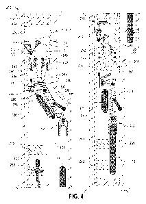
manufacturing and subtractive machining steps. The phase-adjustment elements
500
are preferably produced by an additive manufacturing method.
21
CA 03234143 2024- 4- 5
PTS-0033-CA
[00116] In one embodiment, the module is produced entirely
from metal, for
example aluminum, by additive manufacturing.
[00117] In another embodiment, the module 1 comprises a core
made from polymer,
PEEK, metal or ceramic, and a conductive coating deposited on the faces of
this core.
The core of the module 1 may be formed from a polymer material, ceramic, a
metal or
an alloy, for example from aluminum, titanium or steel. The phase-adjustment
elements
500 may be integrated into the core and formed from the same material as the
core.
The conductive coating may cover the phase-adjustment elements 500.
[00118] The core of the module 1 may be produced by
stereolithography or by
selective laser melting. The core may comprise different parts that are
assembled
together, for example by gluing or welding. In this case, the phase-adjustment
elements
500 may be added to the core and associated with the core by gluing or
welding.
[00119] The metal layer forming the coating may comprise a
metal chosen from Cu,
Au, Ag, Ni, Al, stainless steel, brass or a combination of these metals.
[00120] One or more of the inner and outer surfaces of the core, including
the phase-
adjustment elements 500, may be covered with a conductive metal layer, for
example
copper, silver, gold, nickel etc., plated by electroless deposition. The
thickness of this
layer is, for example, between 1 and 20 micrometers, for example between 4 and
10
micrometers.
[00121] The thickness of this conductive covering must be sufficient for
the surface
to be electrically conductive at the chosen radio frequency. This is typically
achieved
using a conductive layer with a thickness greater than the depth of skin 6.
[00122] This thickness is preferably substantially constant
over all of the inner
surfaces in order to obtain a finished part that has precise dimensional
tolerances.
[00123] The conductive metal can be deposited on the inner and possibly
outer faces
by submerging the core in a series of successive baths, typically between 1
and 15 baths.
22
CA 03234143 2024- 4- 5
PTS-0033-CA
Each bath involves a fluid with one or more reagents. The deposition does not
require
current to be applied to the core that is to be covered. Stirring and even
deposition are
achieved by moving the fluid, for example by pumping the fluid through the
transmission
channel and/or around the module 1 or by vibrating the core and/or the tank of
fluid,
for example with an ultrasonic vibrating device, to create ultrasonic waves.
[00124] The conductive metal coating may cover all of the
faces of the core in an
uninterrupted manner. In another embodiment, the module 1 comprises side walls
with
outer and inner surfaces, the inner surfaces delimiting a channel, said
conductive
coating covering said inner surface but not all of the outer surface.
[00125] The module 1 may comprise a smoothing layer intended to at least
partially
smooth irregularities on the surface of the core. The conductive coating is
deposited
over the smoothing layer.
[00126] The module 1 may comprise a primer (or adhesion)
layer deposited on the
core so as to cover it in an uninterrupted manner.
[00127] The primer layer may be made from conductive or non-conductive
material.
The primer layer helps improve the adhesion of the conductive layer to the
core. Its
thickness is preferably less than the roughness Ra of the core, and less than
the
resolution of the method of additive manufacturing used to manufacture the
core.
[00128] In one embodiment, the module 1 successively
comprises a non-conductive
core produced by additive manufacturing, including one or more phase-
adjustment
elements 500, a primer layer, a smoothing layer and a conductive layer.
Therefore, the
primer layer and the smoothing layer help reduce the roughness of the surface
of the
waveguide channel. The primer layer helps improve the adhesion of the
conductive or
non-conductive core with the smoothing layer and the conductive layer.
[00129] The shape of the module 1 may be determined by a computer file
stored on
a data storage medium and used to control an additive manufacturing device.
23
CA 03234143 2024- 4- 5
PTS-0033-CA
[00130] Furthermore, the shape, number, location, dimensions
and any other useful
parameter relating to the phase-adjustment elements 500 may be determined by a
computer file stored on a data storage medium and used to control an additive
manufacturing device.
[00131] Alternatively, or additionally, the shape, number, location,
dimensions and
any other useful parameter relating to the phase-adjustment elements 500 may
be
determined in full or in part by means of a modeling program. Such a program
can be
used, for example, to determine at least some of the characteristics of the
phase-
adjustment elements 500 that are needed in order to eliminate or modulate the
phase
shift, depending on the characteristics of the waveguides that are used. Such
a modeling
program may, for example, take into account the length of the waveguide in
question,
its longitudinal shape, including curves, the shape of its cross section, and
any other
useful parameter, as well as the wavelength of the signal. The modeling may
include
applying an algorithm for determining the phase shift of a waveguide depending
on its
characteristics. It may include applying an algorithm, for example an
analytical or
successive approximation algorithm, for determining one or more
characteristics of the
phase-adjustment elements 500 needed to correct, control or eliminate this
phase shift.
The characteristics of the phase-adjustment elements 500 include one or more
of their
dimensions, their shapes, how many of them there are, and their arrangement in
the
waveguide, including their orientation and location.
[00132] An artificial intelligence and/or deep learning
module may be used to
determine the effect of the phase-adjustment elements 500 on the phase shift
and the
transfer function of the waveguides. When the characteristics of the phase-
adjustment
elements are determined, they may be transferred to an additive manufacturing
device
in order to produce them.
[00133] The module may be connected to an electronic circuit,
for example in the
form of a printed circuit mounted behind the third layer 5 of ports or behind
the fourth
layer 6, with amplifiers and/or phase shifters connected to each port.
24
CA 03234143 2024- 4- 5